samsung 4g nand flash memory maven see test … 4g nand flash memory maven see test report timothy...
TRANSCRIPT

T042011_K9F4G08U0A
1
Samsung 4G NAND Flash Memory MAVEN SEE
Test Report
Timothy Oldham Jonathan Pellish, Alvin Boutte Test Date: April 20, 2011 Report Date: March 15, 2012
I. Introduction
This study was undertaken to determine and compare the susceptibilities of 4 Gbit NAND Flash memories from Samsung (part number K9F4G08U0A) to destructive and nondestructive single-event effects (SEE) for the NASA MAVEN mission. The devices were monitored for SEUs, errors from individual cells, for SEFIs, errors arising in the control logic, and for destructive events, including latchup, induced by exposing them to a heavy ion beam at the Texas A&M University Cyclotron. This same part had been tested extensively for the NASA MMS mission, and the results obtained in this test have been compared to the previous results, in some cases. The reports on the previous tests provide more details [1, 2].
II. Devices Tested
In this test, four parts were used (part number K9F4G08U0A-PCB0, Lot Date Code (LDC) 0804). The parts have 512Mx8 organization with large blocks. That is, the blocks are 128Kx8, with 64 pages/block. Each page is nominally 2Kx8, but they also have 64 redundant columns, which makes the total page size 2112x8. NAND flash normally has some bad blocks which can be screened off. The specification is that no more than 80 of the 4096 blocks will be bad. In our experience, the parts almost always have a few bad blocks, but it is usually a single digit number. Note that with commercial devices, the same lot date code is no guarantee that the devices are from the same wafer diffusion lot or even from the same fabrication facility.
The device technology is 73 nm minimum feature size CMOS NAND Flash memory. All the parts are single die, SLC (single level cells). The chips came in a 48-pin TSOP package, which is an industry standard package, but the plastic had been dissolved on the topside to expose the chips, allowing the beam to reach the chip surface.

T042011_K9F4G08U0A
2
Fig. 1. Photo of Samsung 4G NAND flash die.
III. Test Facilities
Facility: Texas A&M University Cyclotron Flux: (5 x 10³ to 1. x 105 particles/cm2/s). Fluence: All tests were run to 1E3 to 1E8 ions/cm2, or until destructive or functional events occurred.
Table I: Ions/Energies and LET for this test
TAMU Ions
Energy/ AMU
Energy (MeV)
Approx. LET incident on die surface (MeV•cm2/mg)
Angles Effective LET
Ne 15 300 2.7 0, 45 2.8, 3.9
Ar 15 600 8.4 0,45 8.4, 11.8
Kr 15 1260 30.1 0, 45 29.3, 41
IV. Test Conditions
Test Temperature: Room Temperature. Operating Frequency: (0-40 MHz). Power Supply Voltage: 3.3V. Standard test methods for SEU testing (e.g., ASTM 1192) call for
testing at nominal voltage less 10%, because SEU in standard volatile memories is caused by voltages being pulled down. However, flash memories are designed to retain information even at zero volts, so the

T042011_K9F4G08U0A
3
upset mechanisms are clearly different, here. In addition, we are also looking for control logic errors, which are thought to be due to things turning on when they are not supposed to be on. Reduced voltage would cause an underestimate of the rate for these events. Therefore, we used nominal voltage, 3.3 V, in all tests.
V. Test Methods
Because Flash technology uses different voltages and circuitry depending on the operation being performed, testing was performed for a variety of test patterns and bias and operating conditions.
Test patterns included all 0’s, all 1’s, checkerboard and inverse checkerboard. In general, all zeroes is the worst-case condition for single bit errors. For a zero, the floating gate is fully charged with electrons. An ion can have the effect of introducing positive charge, which may be enough to cause a zero-to-one error. However, a checkerboard pattern (AA) was used in many tests because errors in the control circuitry can cause errors of both polarities. One-to-zero errors are an indication that the errors are coming from the control circuits. Between exposures, all patterns can used to exercise the DUT, to verify that it was still fully functional. However, all patterns are not used routinely, just because it is too time consuming to do so. The maximum clock frequency for these devices was 40 MHz, which is also the frequency used in the dynamic testing.
Bias and operating conditions included:
1) Static/Unbiased irradiation, in which a pattern was written and verified, and then bias was removed from the part and the part was irradiated. Once the irradiation reached the desired fluence, it was stopped, bias was restored, and the memory contents were read and errors tallied.
2) Static irradiation, which was similar to unbiased irradiation, except that bias was maintained throughout irradiation of the part.
Note that these conditions provide no opportunity to monitor functional or hard failures that may occur during the irradiation. It was also not possible to monitor the power supply current during the unbiased tests, but this was done in all the other test modes.
3) Dynamic Read, in which a pattern was written to memory and verified, then subsequently read continuously during irradiation, and the errors counted. This condition allows determination of functional, configuration and hard errors, as well as bit errors. In this mode, the number of static bit errors is determined by reading the memory again, after the beam is turned off.
4) Dynamic Read/Erase/Write, which again was similar to the Dynamic Read, except that a word in error was first erased and then rewritten. In this mode, the words that are read are compared to the stored pattern. When errors are detected, the addresses are erased and rewritten. Because the Erase and Write operations use the charge pump, it is expected that the Flash could be more vulnerable to destructive conditions during these operations.
5) In this set of experiments, we have attempted to look at angular effects, which may include multiple bits grazed by the same ion, and other effects due to charge sharing by multiple nodes in the control logic. This test was done with the DUT tilted 45 degrees, which was close to the maximum possible angle, because the socket would have blocked the beam at angles much higher. However, previous testing of this part [1, 2] has shown that destructive

T042011_K9F4G08U0A
4
failures occur primarily at normal incidence. For this reason, a majority of the shots were taken at normal incidence.
The Block diagram for control of the DUT is shown in Figure 2. The FPGA based controller interfaces to the FLASH daughter card and to a laptop, allowing control of the FPGA and uploading of new FPGA configurations and instructions for control of the DUT. Power for the flash is supplied by means of a computer-controlled power supply. The National Instruments Labview interface monitors the power supply for over-current conditions and shuts down power to the DUT if such conditions are detected.
Figure 2. Overall Block Diagram for the testing of the NAND Flash.
T042011_K9F4G08U0A
5
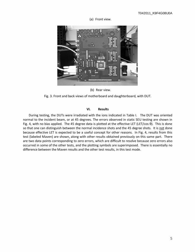
(a) Front view.
(b) Rear view.
Fig. 3. Front and back views of motherboard and daughterboard, with DUT.
VI. Results
During testing, the DUTs were irradiated with the ions indicated in Table I. The DUT was oriented normal to the incident beam, or at 45 degrees. The errors observed in static SEU testing are shown in Fig. 4, with no bias applied. The 45 degree data is plotted at the effective LET (LET/cos θ). This is done so that one can distinguish between the normal incidence shots and the 45 degree shots. It is not done because effective LET is expected to be a useful concept for other reasons. In Fig. 4, results from this test (labeled Maven) are shown, along with other results obtained previously on this same part. There are two data points corresponding to zero errors, which are difficult to resolve because zero errors also occurred in some of the other tests, and the plotting symbols are superimposed. There is essentially no difference between the Maven results and the other test results, in this test mode.

T042011_K9F4G08U0A
6
1x100
Effective LET (MeV•cm2/mg)
Cro
ss S
ectio
n(c
m2 /
devi
ce) 1x10⁻¹
1x10⁻²
1x10⁻³
1x10⁻⁴
1x10⁻⁵
1x10⁻⁶
1x10⁻⁷
1x100
1x10⁻¹
1x10⁻²
1x10⁻³
1x10⁻⁸
1x10⁻⁹
1x10⁻¹⁰
0 20 40 60 80 100
2011 SEU2009 SEU2009 SEFI2009 Destructive
Fig. 4. SEU, SEFI, and Destructive results in static, unbiased test mode. 2011 test results are
consistent with 2009 results on the same part.
T042011_K9F4G08U0A
7
1x100
Effective LET (MeV•cm2/mg)
Cro
ss S
ectio
n(c
m2 /
devi
ce)
0 20 40 60 80 100
1x10⁻¹
1x10⁻²
1x10⁻³
1x10⁻⁴
1x10⁻⁵
1x10⁻⁶
1x10⁻⁷
1x100
1x10⁻¹
1x10⁻²
1x10⁻³
1x10⁻⁸
1x10⁻⁹
1x10⁻¹⁰
2011 SEU
2009 SEU2009 SEFI
2011 SEFI
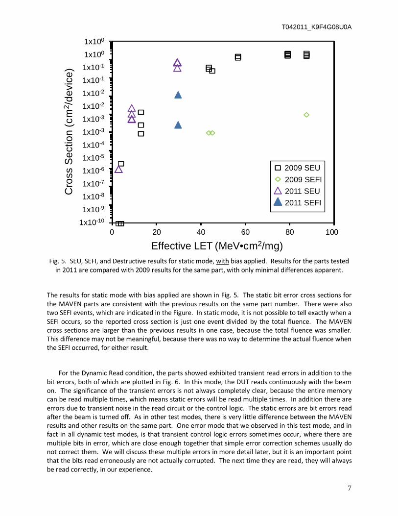
Fig. 5. SEU, SEFI, and Destructive results for static mode, with bias applied. Results for the parts tested
in 2011 are compared with 2009 results for the same part, with only minimal differences apparent.
The results for static mode with bias applied are shown in Fig. 5. The static bit error cross sections for the MAVEN parts are consistent with the previous results on the same part number. There were also two SEFI events, which are indicated in the Figure. In static mode, it is not possible to tell exactly when a SEFI occurs, so the reported cross section is just one event divided by the total fluence. The MAVEN cross sections are larger than the previous results in one case, because the total fluence was smaller. This difference may not be meaningful, because there was no way to determine the actual fluence when the SEFI occurred, for either result.
For the Dynamic Read condition, the parts showed exhibited transient read errors in addition to the bit errors, both of which are plotted in Fig. 6. In this mode, the DUT reads continuously with the beam on. The significance of the transient errors is not always completely clear, because the entire memory can be read multiple times, which means static errors will be read multiple times. In addition there are errors due to transient noise in the read circuit or the control logic. The static errors are bit errors read after the beam is turned off. As in other test modes, there is very little difference between the MAVEN results and other results on the same part. One error mode that we observed in this test mode, and in fact in all dynamic test modes, is that transient control logic errors sometimes occur, where there are multiple bits in error, which are close enough together that simple error correction schemes usually do not correct them. We will discuss these multiple errors in more detail later, but it is an important point that the bits read erroneously are not actually corrupted. The next time they are read, they will always be read correctly, in our experience.

T042011_K9F4G08U0A
8
1x100
Effective LET (MeV•cm2/mg)
Cro
ss S
ectio
n(c
m2 /
devi
ce)
1x10⁻¹
1x10⁻²
1x10⁻³
1x10⁻⁴
1x10⁻⁵
1x10⁻⁶
1x10⁻⁷
1x100
1x10⁻¹
1x10⁻²
1x10⁻³
1x10⁻⁸
1x10⁻⁹
1x10⁻¹⁰
0 20 40 60 80 100
2009 SET2009 Static
2009 SEFI
2011 SET2011 Static
2011 SEFI
Fig. 6. SEU, SEFI, and Destructive results for Dynamic Read mode.
Results for the dynamic R/E/W tests are shown in Fig 7. In this mode, errors are counted as they are
read, but then they are erased and rewritten. Therefore, there are no static errors read after the beam is turned off, and bits in error for a time are counted as transient errors. Because the high voltage erase and program operations are performed constantly, it was expected there would be errors in the control logic in this mode, and there were, as we will discuss. As in all the other test modes, there is very little difference between results on MAVEN parts and previous results on the same part number. There was one functional failure in this test mode, which is indicated in Fig. 7 by the red triangle at LET approximately 30 MeV/mg/cm2. The other red triangles indicate failures in previous testing. Although we plot these failures as shown in Fig. 7, which suggests they are due to single ion interactions, there is a clear pattern in most of the data indicating that the failures are actually due to cumulative damage over many beam runs. Fig. 8a shows the current history for one of the MAVEN parts at the beginning of the test run, where current levels are all normal for a fresh part. This shot was in static mode with bias applied, so the current level was about 1 mA, or less, when the beam was on. After the beam was off, there is a Read, with current about 10 mA, to count the errors. Then there is an Erase operation, with current about 8 mA, followed by a Write operation, with current about 17 mA, to store the pattern for the next shot. Then there is another Read, current about 10 mA again, to verify that the Erase and Write operations were successful. In Fig. 8b, another trace for the same part is shown for a run in Read/Erase/Write mode, but more than 30 beam runs later, and the Write current has crept up to about 26 mA. This is a normal trend—gradually increasing Write current over many beam runs, with functional failure finally occurring soon after the Write current goes above 25 mA. For the DUT used in Fig. 8, the cumulative fluence was more than 1.5x10⁸ ions/cm2, at all LETs. The DUT used in Fig. 8 was retired soon

T042011_K9F4G08U0A
9
after Fig 8b, because it was recognized that failure from cumulative damage was imminent. In previous testing of this part, many of the failures happened because the test was continued until failure. Results for the part that failed in the MAVEN test are shown in Fig. 9. The part was a fresh part, on its first beam run, being tested in R/E/W mode, with normal results initially. It was Reading with 10 mA current levels as expected, until the system started detecting errors, at which point the current level increased to about 15-17 mA, which is the normal Write current level. After a time, though, the write current increases abruptly to more than 50 mA, which usually means the part has failed. In this case, the part was still fully functional—it was reset and used again on the next run, but it suffered functional failure on that run. The total fluence for both runs was 1.4x10⁴ Kr ions/cm2. According to the input spectrum for the CREME96 code [3], the flux of ions at or above the LET of Kr, in geosynchronous orbit or interplanetary space, is about one ion/cm2 every 18 years. Therefore, the measured fluence to failure corresponds to about 250,000 chip years in space. In previous tests, there were no functional failures at all at the LET of Kr, and no other DUTS failed at this LET in this test, so the actual failure rate may be much lower.
00 20 40 60 80 100
1x100
Effective LET (MeV•cm2/mg)
Cro
ss S
ectio
n(c
m2 /d
evic
e)
1x10⁻¹
1x10⁻²
1x10⁻³
1x10⁻⁴
1x10⁻⁵
1x10⁻⁶
1x10⁻⁷
1x100
1x10⁻¹
1x10⁻²
1x10⁻³
1x10⁻⁸
1x10⁻⁹
1x10⁻¹⁰
2009 SET2009 Static
2009 SEFI
2011 SET
2009 Destructive2011 SEFI
2011 Destructive
Fig. 7. SEU, SEFI, and Destructive results in Dynamic Read/Erase/Write mode.

T042011_K9F4G08U0A
10
-5x10⁻³
0
5x10⁻³
1x10⁻²
1.5x10⁻²
2x10⁻²
Time (Minutes)
Cur
rent
(A)
1 2 3 40
(a)
0 1 2 3 4
3.0x10⁻²
Time (Minutes)
Cur
rent
(A)
2.5x10⁻²
2.0x10⁻²
1.5x10⁻²
1.0x10⁻²
5.0x10⁻³
-5.0x10⁻³
0
(b)
Fig 8. (a) Current history for fresh Samsung 4G NAND part, and (b) the same part near end-of-life, where Write current has increased from about 17 mA to 26 mA, from cumulative damage.

T042011_K9F4G08U0A
11
0 10 20 30
7x10⁻²
Time (Seconds)
Cur
rent
(A)
6x10⁻²
5x10⁻²
4x10⁻²
3x10⁻²
2x10⁻²
1x10⁻²
-1x10⁻²
0
Fig. 9. Current history for Samsung 4G NAND in R/E/W mode, just before functional failure.
VII. Discussion
To estimate the error rate expected in space, given the cross sections in Figs. 4-7, we did one CRÈME96 run for geosynchronous orbit, which is essentially the same as interplanetary space, using the following Weibull parameters: threshold LET=2.8, Width =37, exponent = 5, and saturation cross section = 7.5e-11 square microns. This curve bounds all four of the measured cross sections, with some margin in all cases. The result was a bit error rate of 6.35e-12 errors/bit-day, which is approximately five orders of magnitude better than a typical volatile memory. For a 4G memory, this is equivalent to 0.025 errors/chip-day, or about 25 bit-errors per day for a system with, say, 1000 chips. Handling this error rate should be well within the capabilities of error-correcting software. SEFIs are more difficult to correct, but, as Figs. 4-7 show, the cross section is typically 3-4 orders of magnitude less than the bit error cross section, even on shots where SEFIs occur. However, most shots have no SEFIs. For example, in the MAVEN testing, there were four SEFIs on 47 beam runs. For this reason, the average cross-section is really much lower than the Figures indicate. Based only on the cross-sections in Figs. 4-7, the system SEFI rate, assuming 1000 chips, is estimated to be .0025-.025 events/day, or one event every 40-400 days. Based on all shots, the rate is perhaps an order of magnitude lower. Most of these can be corrected by cycling power, and reprogramming the corrupted portion of the memory, so the impact to the mission should be manageable.
Most of the functional failures that were observed were in the previous testing of this part, with Xe ions, which were not used in the MAVEN test, at all. The cross section for functional failures is 10-4-10-5 cm2 at the LET of Xe. At this LET, the flux in interplanetary space is about one ion/cm2 every 125 years,

T042011_K9F4G08U0A
12
according to the CREME96 input spectrum [3]. Therefore, one would expect a functional failure rate between one every 1.25 million and 12.5 million chip-years in space, which should be manageable.
Finally, we observed one unexpected error mode, which should be pointed out, although it appears to be manageable. In all the dynamic test modes, there were occasional errors that occurred in pairs, or sometimes in groups larger than two. These appear to be attributable to transient noise in the control logic. A few examples are shown in Table II, highlighted in yellow. In Table II, the error count is shown, followed by the data read, in decimal form, followed in turn by the expected or stored pattern, also in decimal form. If the expected data is zero, the pattern is all zeroes. If the expected data is a checkerboard pattern, (AA, or 10101010), the decimal equivalent is 170. The next column is “bits in error”, which is always one. From the difference between the actual data and the expected data, one can tell that the errors are always zero-to-one errors. Then the next three columns are the address where the errors occur, block, page, and column. Multiple errors are always in the same block and page, and usually separated by 16 or 18 columns, as shown in Table II. Within each group, the same bit is always in error. For example, in the sixth group of errors, the bit in the “ones” place is in error at all five locations. For the seventh group, the error is in the 64 position, in all six addresses. The last column is just a counter, to keep track of the number of multiple errors. We call attention to these errors because most of them would not be corrected by a simple SEC-DED (Single Error Correction-Double Error Detection) Hamming code, which is the normal error correction for these parts. The Samsung 4G has 64 redundant addresses per page for error correction, so 2048 columns (bytes) out of 2112 can be used for data storage, with the rest used for error correction. This is enough space for error correction to install SEC-DED Hamming code capable of correcting one bit out of every 512 bits, or one bit out of 64 bytes. Since these double or multiple errors are much less than 64 bytes apart, most of them would be treated as uncorrectable double errors by the error correction system. However, it is important to realize that these are only transient errors—that is, they are erroneous Reads, and not static errors. The bits being read are not actually corrupted. In the dynamic test modes, we typically loop through the entire memory, reading the same location several times, and the same multiple errors have never been observed again on the next Read. Therefore, a plausible strategy for dealing with such errors would seem to be, if such an error is detected, to stop and read the appropriate portion of the memory again. If no error is detected on the second Read, then continue normally. We also note that in the entire 47 beam runs of the MAVEN test, there were three pairs of static errors close enough together to defeat SEC-DED error correction. These appear to be due to different ions, hitting in almost the same location. The flux in space is many orders of magnitude is many orders of magnitude less than in an accelerator test, so it is likely that, in space, these ions, and the corresponding errors, would be separated by thousands, or even hundreds of thousands of years.

T042011_K9F4G08U0A
13
Table II. Examples from two different runs of double or multiple errors caused by transients in the control logic.
ERRCnt DATA EXP BIE BLOCK PAGE COL 1 2 0 1 2509 13 907 1
2 2 0 1 2509 13 925 3 32 0 1 2538 37 1245 4 1 0 1 2540 58 1328 5 16 0 1 2541 8 779 6 32 0 1 2542 39 1208 7 128 0 1 2543 36 1234 2
8 128 0 1 2543 36 1252 9 2 0 1 2577 47 952 10 16 0 1 2586 20 718 11 32 0 1 2587 57 1783 3
12 32 0 1 2587 57 1801 13 32 0 1 2602 0 1155 17 4 0 1 2658 24 1773 18 4 0 1 2674 26 1767 19 64 0 1 2697 45 318 20 16 0 1 2711 20 1386 4
21 16 0 1 2711 20 1404 22 32 0 1 2714 29 1226 23 32 0 1 2714 29 1244 24 8 0 1 2728 33 771 5
25 8 0 1 2728 33 789
110 186 170 1 107 20 860 111 171 170 1 110 31 785 112 171 170 1 116 63 1603 6
113 171 170 1 116 63 1619 114 171 170 1 116 63 1621 115 171 170 1 116 63 1639 116 171 170 1 116 63 1657 117 171 170 1 124 26 586 118 171 170 1 124 35 454 128 171 170 1 206 15 904 129 234 170 1 218 57 435 130 234 170 1 234 55 1160 7
131 234 170 1 234 55 1162 132 234 170 1 234 55 1178 133 234 170 1 234 55 1180 134 234 170 1 234 55 1196 135 234 170 1 234 55 1198
T042011_K9F4G08U0A
14
VIII. Conclusions
All flash memory has a bit upset rate that is outstanding, compared to typical volatile memories. The reason is that volatile memories lose information when ion strikes pull down voltages, but flash is designed to retain information, even with no voltage applied. Therefore flash is typically five or more orders of magnitude better than volatile memories in upset rate, and these Samsung parts are no exception. SEFIs are a more significant problem than bit errors in advanced flash memories, and, of course, destructive events are potential show stoppers. Although both of these things have been observed in the Samsung 4G NAND flash memory, the rates appear to be relatively low.
IX. References
1. T.R. Oldham, M.R. Friendlich, A.B. Sanders, H.S. Kim, and M.D. Berg, Heavy Ion SEE Test Report
for the Samsung 4Gbit NAND Flash Memory for MMS, 6/18/2009. http://radhome.gsfc.nasa.gov 2. T.R. Oldham, M.R. Friendlich, A.B. Sanders, C.M. Seidleck, H.S. Kim, M.D. Berg, and K.A. LaBel,
TID and SEE Response of Advanced Samsung and Micron 4G NAND Flash Memories for the NASA MMS Mission, IEEE Radiation Effects Data Workshop Record, pp. 114-122, Quebec, Canada, 2009.
3. A.J. Tylka, J.H. Adams, P.R. Broberg, B. Brownstein, W.F. Dietrich, E.O. Flueckiger, E.L. Petersen, M.A. Shea, D.F. Smart, and E.C. Smith, CREME96: a revision of the Cosmic Ray Effects on Micro-Electronics code, IEEE Trans. Nucl. Sci., vol. 44, no. 6, pp. 2150-2160, Dec. 1997.