sara-n2 - u-blox series modules are a narrow band internet of things (nb-iot) solution coming in the...
TRANSCRIPT

SARA-N2 Power-optimized NB-IoT (LTE Cat NB1) modules Data Sheet
Abstract
Technical data sheet describing SARA-N2 Narrowband Internet of Things cellular modules. These modules are a complete and cost efficient solution offering single-band data transmission for the Internet of Things technology in a compact form factor.
www.u-blox.com
UBX-15025564 - R13

SARA-N2 - Data Sheet
UBX-15025564 - R13 Contents
Page 2 of 28
Document Information
Title SARA-N2
Subtitle Power-optimized NB-IoT (LTE Cat NB1) modules
Document type Data Sheet
Document number UBX-15025564
Revision and date R13 22-Feb-2018
Disclosure restriction
Product Status Corresponding content status
Functional Sample Draft For functional testing. Revised and supplementary data will be published later.
In Development /
Prototype Objective Specification Target values. Revised and supplementary data will be published later.
Engineering Sample Advance Information Data based on early testing. Revised and supplementary data will be published later.
Initial Production Early Prod. Information Data from product verification. Revised and supplementary data may be published later.
Mass Production /
End of Life Production Information Final product specification.
This document applies to the following products:
Name Type number Modem version Application version PCN reference Product status
SARA-N200 SARA-N200-02B-00 06.57 A07.03 UBX-18005015 Initial Production
SARA-N201 SARA-N201-02B-00 06.57 A07.03 UBX-18005015 Initial Production
SARA-N210 SARA-N210-02B-00 06.57 A07.03 UBX-18005015 Initial Production
SARA-N211 SARA-N211-02X-00 06.57 A03.02 UBX-17057306 Engineering Sample
SARA-N280 SARA-N280-02B-00 06.57 A07.03 UBX-18005015 Initial Production
u-blox reserves all rights to this document and the information contained herein. Products, names, logos and designs described herein may in whole or in part be subject to intellectual property rights. Reproduction, use, modification or disclosure to third parties of this document or
any part thereof without the express permission of u-blox is strictly prohibited.
The information contained herein is provided “as is” and u-blox assumes no liability for the use of the information. No warranty, either express or implied, is given, including but not limited, with respect to the accuracy, correctness, reliability and fitness for a particular purpose
of the information. This document may be revised by u-blox at any time. For most recent documents, visit www.u-blox.com.
Copyright © 2018, u-blox AG.
u-blox is a registered trademark of u-blox Holding AG in the EU and other countries.

SARA-N2 - Data Sheet
UBX-15025564 - R13 Contents
Page 3 of 28
Contents
Contents .............................................................................................................................. 3
1 Functional description .................................................................................................. 5
1.1 Overview .............................................................................................................................................. 5
1.2 Product features ................................................................................................................................... 5
1.3 Block diagram ....................................................................................................................................... 6
1.4 Product description ............................................................................................................................... 6
1.5 AT command support ........................................................................................................................... 7
1.6 Supported features ............................................................................................................................... 7
2 Interfaces ...................................................................................................................... 8
2.1 Power management ............................................................................................................................. 8
2.1.1 Module supply input (VCC) ........................................................................................................... 8
2.1.2 Digital I/O interfaces supply output (V_INT) .................................................................................... 8
2.2 Antenna ............................................................................................................................................... 8
2.2.1 Antenna RF interface (ANT) ........................................................................................................... 8
2.2.2 Antenna detection (ANT_DET) ....................................................................................................... 8
2.3 System functions .................................................................................................................................. 8
2.3.1 Module power-on ......................................................................................................................... 8
2.3.2 Module power-off ......................................................................................................................... 8
2.3.3 Module reset ................................................................................................................................. 8
2.4 SIM interface ........................................................................................................................................ 9
2.5 Serial interfaces .................................................................................................................................... 9
2.5.1 Asynchronous serial interface (UART) ............................................................................................ 9
2.5.2 Secondary asynchronous serial interface (Secondary UART) ........................................................... 9
2.5.3 DDC (I2C) interface ...................................................................................................................... 10
2.6 GPIO ................................................................................................................................................... 10
3 Pin definition .............................................................................................................. 11
3.1 Pin assignment ................................................................................................................................... 11
4 Electrical specification ................................................................................................ 14
4.1 Absolute maximum rating .................................................................................................................. 14
4.1.1 Maximum ESD ............................................................................................................................. 14
4.2 Operating conditions .......................................................................................................................... 15
4.2.1 Operating temperature range ...................................................................................................... 15
4.2.2 Supply/power pins ....................................................................................................................... 15
4.2.3 Current consumption .................................................................................................................. 16
4.2.4 RF characteristics ......................................................................................................................... 16
4.2.5 RESET_N pin ................................................................................................................................ 17
4.2.6 SIM interface pins ........................................................................................................................ 17
4.2.7 UART interface pins ..................................................................................................................... 17
SARA-N2 - Data Sheet
UBX-15025564 - R13 Contents
Page 4 of 28
4.2.8 Generic Digital Interface pins ....................................................................................................... 17
5 Mechanical specifications .......................................................................................... 18
6 Qualification and approvals ...................................................................................... 19
6.1 Reliability tests .................................................................................................................................... 19
6.2 Approvals ........................................................................................................................................... 19
6.2.1 ATEX certification ........................................................................................................................ 20
7 Product handling ........................................................................................................ 21
7.1 Packaging ........................................................................................................................................... 21
7.1.1 Reels ........................................................................................................................................... 21
7.1.2 Tapes .......................................................................................................................................... 22
7.2 Moisture Sensitivity Levels ................................................................................................................... 23
7.3 Reflow soldering ................................................................................................................................. 23
7.4 ESD precautions.................................................................................................................................. 23
8 Labeling and ordering information ........................................................................... 24
8.1 Product labeling.................................................................................................................................. 24
8.2 Explanation of codes .......................................................................................................................... 25
8.3 Ordering codes ................................................................................................................................... 25
Appendix .......................................................................................................................... 26
A Glossary ...................................................................................................................... 26
Related documents .......................................................................................................... 27
Revision history ................................................................................................................ 27
Contact .............................................................................................................................. 28

SARA-N2 - Data Sheet
UBX-15025564 - R13 Functional description
Page 5 of 28
1 Functional description
1.1 Overview
SARA-N2 series modules are a Narrow Band Internet of Things (NB-IoT) solution coming in the miniature SARA LGA form factor (26.0 x 16.0 mm, 96-pin). The modules offer IoT data communication over an extended operating temperature range of –40 to +85 °C, with extremely low power consumption.
The SARA-N2 series includes variants supporting single-band and dual-band communication and designed to operate in the frequency range of the LTE bands 5, 8, 20 and 28. These products are ideally suited to battery-powered IoT applications characterized by occasional communications of small amounts of data.
SARA-N2 modules are the optimal choice for IoT devices designed to operate in locations with a very limited coverage and requiring low energy consumption to permit a very long operating life of the primary batteries. Examples of applications include and are not limited to: smart grids, smart metering, telematics, street lighting, environmental monitoring and control, security and asset tracking.
1.2 Product features
Module Region Bands Positioning Interfaces Features Grade
3G
PP R
ele
ase
Base
line
3G
PP C
ate
gory
NB-IoT b
andss
GN
SS v
ia m
odem
Ass
istN
ow
Soft
ware
CellL
oca
te®
UA
RT
USB 2
.0
SPI
DD
C (
I2C
)
GPIO
Ante
nna s
uperv
isor
Pow
er
Save
Mode
eD
RX
Dee p
sle
ep m
ode
Em
bedded U
DP s
tack
CoA
P
FW u
pdate
ove
r A
T (
FOA
T)
FW u
pdate
ove
r th
e a
ir (
FOTA
)
Sta
ndard
Pro
fess
ional
Auto
motive
SARA-N200 Europe
APAC 13 NB1 8 2 ● ● ● ● ● ● ● ●
SARA-N201 APAC 13 NB1 5 2 ● ● ● ● ● ● ● ●
SARA-N210 Europe 13 NB1 20 2 ● ● ● ● ● ● ● ●
SARA-N211 Europe 13 NB1 8,20 2 ● ● ● ● ● ● ● ●
SARA-N280 S.America
APAC 13 NB1 28 2 ● ● ● ● ● ● ● ●
Table 1: SARA-N2 series main features summary
SARA-N2 - Data Sheet
UBX-15025564 - R13 Functional description
Page 6 of 28
1.3 Block diagram
Memory
V_INT
38.4 MHz 32.768 kHz
RF Transceiver
PowerManagement
Baseband
ANT SAWFilter
Switch
PA
VCC (Supply)
DDC (I2C)
UART
SIM
Secondary UART
RESET_N
GPIO
Antenna detection
Figure 1: SARA-N2 series block diagram
The “02" product versions of SARA-N2 modules do not support the following interfaces, which should not be driven by external devices:
o DDC (I2C) interface
o GPIO2 pin
o Antenna detection interface
1.4 Product description
Item SARA-N200 SARA-N201 SARA-N210 SARA-N211 SARA-N280
NB-IoT protocol stack 3GPP Release 13 3GPP Release 13 3GPP Release 13 3GPP Release 13 3GPP Release 13
Operating band Band 8 Band 5 Band 20 Band 8
Band 20
Band 28
Deployment modes In-Band
Guard-Band
Standalone
In-Band
Guard-Band
Standalone
In-Band
Guard-Band
Standalone
In-Band
Guard-Band
Standalone
In-Band
Guard-Band
Standalone
Power Class Class 3 (23 dBm) Class 3 (23 dBm) Class 3 (23 dBm) Class 3 (23 dBm) Class 3 (23 dBm)
Data rate LTE category NB1:
Up to 62.5 kb/s UL
Up to 27.2 kb/s DL
LTE category NB1:
Up to 62.5 kb/s UL
Up to 27.2 kb/s DL
LTE category NB1:
Up to 62.5 kb/s UL
Up to 27.2 kb/s DL
LTE category NB1:
Up to 62.5 kb/s UL
Up to 27.2 kb/s DL
LTE category NB1:
Up to 62.5 kb/s UL
Up to 27.2 kb/s DL
Table 2: SARA-N2 series NB-IoT characteristics summary

SARA-N2 - Data Sheet
UBX-15025564 - R13 Functional description
Page 7 of 28
1.5 AT command support
The SARA-N2 modules support AT commands according to the 3GPP standards, plus the u-blox AT command extension.
For the complete list of all supported AT commands and their syntax, see the SARA-N2 series AT Commands Manual [1].
1.6 Supported features
Feature Description
Network Indication Pin configured to indicate the network status: registered home network, registered roaming, data call enabled, no service. The feature can be enabled through the +UGPIOC AT command.
Embedded UDP stack Embedded UDP/IP stack for UDP sockets.to establish a transparent end-to-end communication.
CoAP The Constrained Application Protocol (CoAP) is a datagram-based client/server application protocol for devices on the constrained network (e.g. low overhead, low-power), designed to easily translate to HTTP for
simplified integration with the web. CoAP clients can use the GET, PUT, POST and DELETE methods using requests and responses with a CoAP server.
Release Assistance The Release Assistance feature introduced in 3GPP Rel.13 allows the module to request for the RRC connection to be dropped as soon as the message has been received by the network. This feature allows a reduction in the module power consumption.
Self-Registration Support of Self-Registration feature according to CTCC (China Telecom Corporation) and CUCC (China Unicom Corporation) requirements.
Firmware update Over AT commands (FOAT)
Firmware module update over AT command interface.
The feature can be enabled and configured through the +UFWUPD AT command.
Firmware update Over The Air (FOTA)
The Firmware over-the-air (FOTA) component uses the CoAP context to download a FW update package from a dedicated server.
Power Saving Mode (PSM) The Power Saving Mode (PSM) feature, defined in 3GPP Rel.13, allows further reduction of the module current consumption maximizing the amount of time a device can remain in extremely low power deep sleep
mode during periods of data inactivity. It can be activated and configured by the +CPSMS AT command.
Deep-sleep mode The SARA-N2 modules enters in extremely low power deep sleep mode whenever possible, using the internal 32 kHz clock to maintaining an extremely low current consumption. This optimizes the life time of the
battery pack used to supply the system
eDRX Extended mode DRX, based on 3GPP Rel.13, reduces the amount of signaling overhead decreasing the frequency of scheduled measurements and/or transmissions performed by the module. This in turn leads to a
reduction in the module power consumption while maintaining a perpetual connection with the base station
Coverage Enhancement Coverage Enhancements Modes introduced in 3GPP Rel.13 for the NB-IoT system improve the cell signal penetration allowing a 20 dB coverage enhancement over standard GSM systems.
Table 3: Some of the main features supported by SARA-N2 modules

SARA-N2 - Data Sheet
UBX-15025564 - R13 Interfaces
Page 8 of 28
2 Interfaces
2.1 Power management
2.1.1 Module supply input (VCC)
SARA-N2 modules must be supplied through the VCC pins by a DC power supply with nominal voltage of 3.6 V. Voltage must be stable during module operation, taking into account that the current drawn from VCC pins may vary significantly based on the power consumption profile of the NB-IoT system.
2.1.2 Digital I/O interfaces supply output (V_INT)
SARA-N2 modules provide an internally generated supply rail output (V_INT) operating at 1.8 V. This can be used in place of an external discrete regulator to supply external digital interfaces.
The voltage level present at the V_INT pin depends on the module operating mode:
When the radio is off, the voltage level is kept low (i.e. 0 V)
When the radio is on, the voltage level is maintained high (i.e. 1.8 V)
Provide a test point connected to the V_INT pin for diagnostic purpose.
2.2 Antenna
2.2.1 Antenna RF interface (ANT)
The ANT pin has an impedance of 50 and provides the RF antenna interface of SARA-N2 modules.
2.2.2 Antenna detection (ANT_DET)
The ANT_DET pin is an Analog to Digital Converter (ADC) input used to sense the antenna presence evaluating the resistance from the ANT pin to GND by means of an external antenna detection circuit implemented on the application board.
The antenna detection (ANT_DET) interface is not supported by "02" product versions.
2.3 System functions
2.3.1 Module power-on
SARA-N2 modules can be switched on by a rising edge voltage applied to the VCC pins. See section 4.2.2 for more details about the valid supply voltage range.
2.3.2 Module power-off
An abrupt under-voltage shutdown occurs on SARA-N2 modules when the VCC supply voltage drops below the operating range minimum limit (see section 4.2.2).
2.3.3 Module reset
SARA-N2 modules can be reset applying a low voltage level on the RESET_N input pin, which is normally set high by an internal pull-up, for a valid time period (see the section 4.2.5). This causes an “external” or “hardware” reset of the module.
Provide a test point connected to the RESET_N pin for diagnostic purpose.
SARA-N2 - Data Sheet
UBX-15025564 - R13 Interfaces
Page 9 of 28
2.4 SIM interface
A SIM card interface is provided by the VSIM, SIM_IO, SIM_CLK, and SIM_RST pins of SARA-N2 modules, supporting 1.8 V SIM card/chip types.
2.5 Serial interfaces
2.5.1 Asynchronous serial interface (UART)
The UART interface is a 5-wire unbalanced asynchronous serial interface available for communication with an application host processor (AT commands and data communication) and for FW upgrade.
The main characteristics of the interface are the following:
Serial port with RS-232 functionality working at the VCC voltage domain (0 V for low data bit or ON state and ~3.6 V, i.e. VCC, for high data bit or OFF state)
Data lines (RXD as module data output, TXD as module data input)
Hardware flow control lines (CTS as module output, RTS as module input)
The following baud rates are supported: 4800, 9600 (default baud rate), 57600 and 115200 b/s.
Fixed frame format: 8N1 (8 data bits, No parity, 1 stop bit)
The CTS line can be configured as RING indicator, to signal an incoming message received by the module or an URC event, or as Network status indicator (for more details see section 2.6 and the u-blox SARA-N2 Series AT Commands Manual [1], +URING, +UGPIOC AT commands).
For FW upgrade purposes, connect a test point to the RXD and TXD pins.
Hardware flow control function is not supported by "02" product versions.
2.5.2 Secondary asynchronous serial interface (Secondary UART)
The secondary UART interface is a 2-wire unbalanced asynchronous serial interface available for diagnostic purpose, to capture trace diagnostic logs delivered by the module.
The main characteristics of the interface are:
Serial port with RS-232 functionality working at the V_INT voltage domain (0 V for low data bit or ON state and 1.8 V, i.e. V_INT, for high data bit or OFF state)
Data line (GPIO1 as module data output)
No flow control
Fixed baud rate: 921600 b/s
Fixed frame format: 8N1 (8 data bits, no parity, 1 stop bit)
For diagnostic purposes, connect a test point to the GPIO1 pin.
The trace diagnostic log is temporarily stopped when the module is in deep-sleep mode.
SARA-N2 - Data Sheet
UBX-15025564 - R13 Interfaces
Page 10 of 28
2.5.3 DDC (I2C) interface
DDC interface: I2C compatible interface available on the SCL and SDA pins of the module for the
communication with external chips and sensors. The interface provides master mode bi-directional bus communication at a bit-rate up to 100 kb/s. The I
2C interface requires external pull-up resistors. The internal
power domain used by the DDC (I2C) pins is V_INT (1.8 V).
The DDC (I2C) interface is not supported by "02" product versions.
2.6 GPIO
SARA-N2 series modules provide the following pins:
GPIO1 pin, working at the V_INT (1.8 V) voltage domain, supporting the Secondary UART data output functionality (see section 2.5.2 and Table 4)
GPIO2 pin, working at the V_INT (1.8 V) voltage domain, not supported by "02" product versions
CTS pin, working at the VCC (3.6 V typical) voltage domain, supporting the Network status indication and the RING indicator functionality (see section 2.5.1 and Table 4)
For more details about how the pins can be configured, see u-blox SARA-N2 Series AT Commands Manual [1], +UGPIOC, +URING AT commands.
For diagnostic purposes, connect a test point to the GPIO1 pin.
Function Description Default GPIO Configurable GPIOs
Network status indication
Network status: registered home network, registered roaming, data transmission, no service
-- CTS
RING indicator Indicates an incoming message received by the module or an URC event
-- CTS
Secondary UART Secondary UART data output for diagnostic purpose, to
capture diagnostic logs delivered by the module
GPIO1 GPIO1
Pin disabled Tri-state with an internal active pull-down enabled CTS CTS
Table 4: GPIO custom functions configuration

SARA-N2 - Data Sheet
UBX-15025564 - R13 Pin definition
Page 11 of 28
3 Pin definition
3.1 Pin assignment
64 63 61 60 58 57 55 54
22 23 25 26 28 29 31 32
11
10
8
7
5
4
2
1
21
19
18
16
15
13
12
43
44
46
47
49
50
52
53
33
35
36
38
39
41
42
65 66 67 68 69 70
71 72 73 74 75 76
77 78
79 80
81 82
83 84
85 86 87 88 89 90
91 92 93 94 95 96
CTS
RTS
RSVD
RSVD
V_INT
RSVD
GND
RSVD
RESET_N
GPIO1
RSVD
RXD
TXD
3
20
17
14
9
6
24 27 30
51
48
45
40
37
34
5962 56
GND
GND
RSVD
RSVD
GND
RSVD
GND
GND
RSV
D
RSV
D
RSV
D
GN
D
RSV
D
GPIO
2
SD
A
SC
L
RSV
D
GN
D
GN
D
GND
RSVD
RSVD
RSVD
RSVD
GND
VCC
VCC
RSVD
RSVD
RSVD
SIM_CLK
SIM_IO
VSIM
RSVD
VCC
RSVD
RSVD
SIM_RST
RSVD
RSVD
GN
D
GN
D
GN
D
GN
D
GN
D
GN
D
GN
D
GN
D
GN
D
AN
T_D
ET
AN
T
SARA-N2Top View
Pin 65-96: GND
Figure 2: SARA-N2 series modules pin assignment
SARA-N2 - Data Sheet
UBX-15025564 - R13 Pin definition
Page 12 of 28
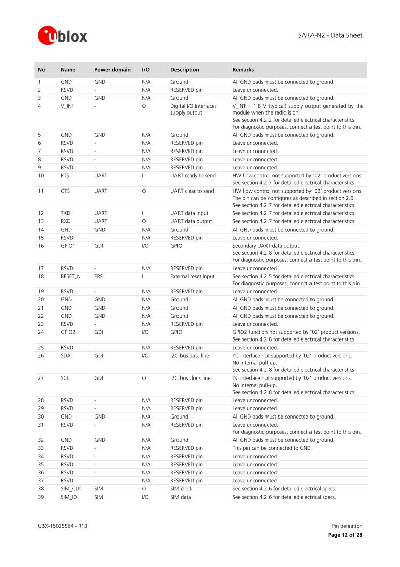
No Name Power domain I/O Description Remarks
1 GND GND N/A Ground All GND pads must be connected to ground.
2 RSVD - N/A RESERVED pin Leave unconnected.
3 GND GND N/A Ground All GND pads must be connected to ground.
4 V_INT - O Digital I/O Interfaces supply output
V_INT = 1.8 V (typical) supply output generated by the module when the radio is on.
See section 4.2.2 for detailed electrical characteristics.
For diagnostic purposes, connect a test point to this pin.
5 GND GND N/A Ground All GND pads must be connected to ground.
6 RSVD - N/A RESERVED pin Leave unconnected.
7 RSVD - N/A RESERVED pin Leave unconnected.
8 RSVD - N/A RESERVED pin Leave unconnected.
9 RSVD - N/A RESERVED pin Leave unconnected.
10 RTS UART I UART ready to send HW flow control not supported by ‘02’ product versions.
See section 4.2.7 for detailed electrical characteristics.
11 CTS UART O UART clear to send HW flow control not supported by ‘02’ product versions.
The pin can be configures as described in section 2.6.
See section 4.2.7 for detailed electrical characteristics.
12 TXD UART I UART data input See section 4.2.7 for detailed electrical characteristics.
13 RXD UART O UART data output See section 4.2.7 for detailed electrical characteristics.
14 GND GND N/A Ground All GND pads must be connected to ground.
15 RSVD - N/A RESERVED pin Leave unconnected.
16 GPIO1 GDI I/O GPIO Secondary UART data output.
See section 4.2.8 for detailed electrical characteristics.
For diagnostic purposes, connect a test point to this pin.
17 RSVD - N/A RESERVED pin Leave unconnected.
18 RESET_N ERS I External reset input See section 4.2.5 for detailed electrical characteristics.
For diagnostic purposes, connect a test point to this pin.
19 RSVD - N/A RESERVED pin Leave unconnected.
20 GND GND N/A Ground All GND pads must be connected to ground.
21 GND GND N/A Ground All GND pads must be connected to ground.
22 GND GND N/A Ground All GND pads must be connected to ground.
23 RSVD - N/A RESERVED pin Leave unconnected.
24 GPIO2 GDI I/O GPIO GPIO2 function not supported by ‘02’ product versions.
See section 4.2.8 for detailed electrical characteristics.
25 RSVD - N/A RESERVED pin Leave unconnected.
26 SDA GDI I/O I2C bus data line I2C interface not supported by ‘02’ product versions.
No internal pull-up.
See section 4.2.8 for detailed electrical characteristics.
27 SCL GDI O I2C bus clock line I2C interface not supported by ‘02’ product versions.
No internal pull-up.
See section 4.2.8 for detailed electrical characteristics.
28 RSVD - N/A RESERVED pin Leave unconnected.
29 RSVD - N/A RESERVED pin Leave unconnected.
30 GND GND N/A Ground All GND pads must be connected to ground.
31 RSVD - N/A RESERVED pin Leave unconnected.
For diagnostic purposes, connect a test point to this pin.
32 GND GND N/A Ground All GND pads must be connected to ground.
33 RSVD - N/A RESERVED pin This pin can be connected to GND.
34 RSVD - N/A RESERVED pin Leave unconnected.
35 RSVD - N/A RESERVED pin Leave unconnected.
36 RSVD - N/A RESERVED pin Leave unconnected.
37 RSVD - N/A RESERVED pin Leave unconnected.
38 SIM_CLK SIM O SIM clock See section 4.2.6 for detailed electrical specs.
39 SIM_IO SIM I/O SIM data See section 4.2.6 for detailed electrical specs.

SARA-N2 - Data Sheet
UBX-15025564 - R13 Pin definition
Page 13 of 28
No Name Power domain I/O Description Remarks
40 SIM_RST SIM O SIM reset See section 4.2.6 for detailed electrical specs.
41 VSIM - O SIM supply output VSIM = 1.80 V typical generated by the module.
See section 4.2.2 for detailed electrical characteristics.
42 RSVD - N/A RESERVED pin Leave unconnected.
43 GND GND N/A Ground All GND pads must be connected to ground.
44 RSVD - N/A RESERVED pin Leave unconnected.
45 RSVD - N/A RESERVED pin Leave unconnected.
46 RSVD - N/A RESERVED pin Leave unconnected.
47 RSVD - N/A RESERVED pin Leave unconnected.
48 RSVD - N/A RESERVED pin Leave unconnected.
49 RSVD - N/A RESERVED pin Leave unconnected.
50 GND GND N/A Ground All GND pads must be connected to ground.
51 VCC VCC I Module supply input All VCC pins must be connected to external supply.
See 4.2.2 and 4.2.3 for detailed electrical characteristics.
52 VCC VCC I Module supply input All VCC pins must be connected to external supply.
See 4.2.2 and 4.2.3 for detailed electrical characteristics.
53 VCC VCC I Module supply input All VCC pins must be connected to external supply.
See 4.2.2 and 4.2.3 for detailed electrical characteristics.
54 GND GND N/A Ground All GND pads must be connected to ground.
55 GND GND N/A Ground All GND pads must be connected to ground.
56 ANT ANT I/O RF antenna 50 nominal characteristic impedance.
See section 4.2.4 for detailed RF characteristics.
57 GND GND N/A Ground All GND pads must be connected to ground.
58 GND GND N/A Ground All GND pads must be connected to ground.
59 GND GND N/A Ground All GND pads must be connected to ground.
60 GND GND N/A Ground All GND pads must be connected to ground.
61 GND GND N/A Ground All GND pads must be connected to ground.
62 ANT_DET ADC I Antenna detection ANT_DET not supported by ‘02’ product versions.
63 GND GND N/A Ground All GND pads must be connected to ground.
64 GND GND N/A Ground All GND pads must be connected to ground.
65-96 GND GND N/A Ground All GND pads must be connected to ground.
Table 5: SARA-N2 series modules pin-out
For an explanation of abbreviations and terms used, see Appendix A.
SARA-N2 - Data Sheet
UBX-15025564 - R13 Electrical specification
Page 14 of 28
4 Electrical specification Stressing the device above one or more of the ratings listed in the Absolute Maximum Rating
section may cause permanent damage. These are stress ratings only. Operating the module at these or at any conditions other than those specified in the Operating Conditions section (section 4.2) of the specification should be avoided. Exposure to Absolute Maximum Rating conditions for extended periods may affect device reliability.
Operating condition ranges define those limits within which the functionality of the device is guaranteed.
Electrical characteristics are defined according to the verification on a representative number of samples or according to the simulation.
Where application information is given, it is advisory only and does not form part of the specification.
4.1 Absolute maximum rating
Limiting values given below are in accordance with the Absolute Maximum Rating System (IEC 134).
Symbol Description Condition Min. Max. Unit
VCC Module supply voltage Input DC voltage at VCC pin 4.25 V
GDI Generic digital interfaces Input DC voltage at Generic digital interfaces pins 2.1 V
SIM SIM interface Input DC voltage at SIM interface pins 2.1 V
UART UART interface Input DC voltage at UART interface pins 4.25 V
ERS External reset signal Input DC voltage at RESET_N pin 4.25 V
Rho_ANT Antenna ruggedness Output RF load mismatch ruggedness at ANT pins 10:1 VSWR
Tstg Storage Temperature -40 85 °C
Table 6: Absolute maximum ratings
The product is not protected against overvoltage or reversed voltages. If necessary, voltage spikes exceeding the power supply voltage specification given in table above must be limited to values within the specified boundaries by using appropriate protection devices.
4.1.1 Maximum ESD
Parameter Min Typical Max Unit Remarks
ESD sensitivity for all pins 1000 V Human Body Model according to JESD22-A114
Table 7: Maximum ESD ratings
u-blox cellular modules are Electrostatic Sensitive Devices and require special precautions when handling. See section 7.4 for ESD handling instructions.

SARA-N2 - Data Sheet
UBX-15025564 - R13 Electrical specification
Page 15 of 28
4.2 Operating conditions
Unless otherwise indicated, all operating condition specifications are at an ambient temperature of 25°C.
Operation beyond the operating conditions is not recommended and extended exposure beyond them may affect device reliability.
4.2.1 Operating temperature range
Parameter Min. Typical Max. Unit Remarks
Operating temperature range -40 +85 °C
-20 +85 °C Normal operating temperature range
-40 -20 °C Extended operating temperature range
Table 8: Environmental conditions
4.2.1.1 Normal operating temperature range
The module is fully functional and meets the 3GPP specification across the specified temperature range.
4.2.1.2 Extended operating temperature range
The module is fully functional across the specified temperature range. Occasional deviations from the 3GPP specification may occur.
4.2.2 Supply/power pins
Pin Name Parameter Min Typ Max Unit
VCC Module supply normal operating input voltage1 3.10 3.60 4.00 V
Module supply extended operating input voltage2 2.75 4.20 V
Table 9: Input characteristics of Supply/Power pins
Pin Name Parameter Min Typ Max Unit
VSIM SIM supply output voltage 1.80 V
V_INT Generic Digital Interfaces supply output voltage 1.80 V
I_INT Generic Digital Interfaces supply output current capability 80 mA
Table 10: Output characteristics of Supply/Power pins
1 Input voltage at VCC pins must be above the normal operating range minimum limit to switch-on the module.
2 Occasional deviations from the 3GPP specifications may occur. The RF power transmitted by the module may be few dB lower than
expected when operating below the minimum value of the normal operating range. Ensure that input voltage at VCC never drops below the extended operating range minimum limit during module operation to avoid possible module switch-off events.

SARA-N2 - Data Sheet
UBX-15025564 - R13 Electrical specification
Page 16 of 28
4.2.3 Current consumption
Mode Band Condition Tx power Min Typ3 Max Unit
Deep-sleep mode - Averaged current over a 10-second period 3 µA
Active mode - Averaged current over a 10-second period 6 mA
Rx-mode All Averaged current over a 10-second period 46 mA
Tx-mode All Averaged current over a 2-second period -40 dBm 74 mA
-7 dBm 75 mA
3 dBm 78 mA
13 dBm 100 mA
23 dBm 220 mA
Table 11: VCC current consumption4
4.2.4 RF characteristics
Parameter Min Max Unit Remarks
Frequency range
Band 5
Uplink 824 849 MHz Module transmit
Downlink 869 894 MHz Module receive
Frequency range Band 8
Uplink 880 915 MHz Module transmit
Downlink 925 960 MHz Module receive
Frequency range Band 20
Uplink 832 862 MHz Module transmit
Downlink 791 821 MHz Module receive
Frequency range Band 28
Uplink 703 748 MHz Module transmit
Downlink 758 803 MHz Module receive
Table 12: Operating RF frequency bands
Parameter Min. Typical Max. Unit Remarks
Maximum output power 23.0 dBm Uplink BPSK/QPSK modulation
Condition: 50 output load
Table 13: Transmitter maximum output power
Parameter Min. Typical Max. Unit Remarks
Receiver input sensitivity -135 dBm Downlink RF level @ BLER MCS-1 < 10 %
Table 14: Receiver sensitivity performance
3 Typical values with a matched antenna.
4 Module current consumption through VCC input pins, in the listed modes/conditions.
SARA-N2 - Data Sheet
UBX-15025564 - R13 Electrical specification
Page 17 of 28
4.2.5 RESET_N pin
Parameter Min. Typical Max. Unit Remarks
Internal supply for External Reset Input Signal
VCC V Module supply input (VCC)
Schmitt Trigger Low to High Threshold Point (V
T+)
0.52*VCC V
Schmitt Trigger High to Low Threshold Point (V
T-)
0.36*VCC V
Pull-up resistance 78 k Internal active pull-up to VCC
Low-level input current -10 µA
RESET_N low-level time 500 ns Low time to reset the module
Table 15: RESET_N pin characteristics
4.2.6 SIM interface pins
Parameter Min. Typical Max. Unit Remarks
Internal supply for SIM domain 1.8 V Generic Digital Interface supply output (VSIM)
Low-level input -0.1*VSIM 0.2*VSIM V
High-level input 0.7*VSIM 1.1*VSIM V
Low-level output 0.0 V
High-level output VSIM V
Internal pull-up on SIM_IO 4.7 k Internal pull-up to VSIM
Clock frequency on SIM_CLK 4.8 MHz
Input / Output leakage current ±10 µA
Table 16: SIM pins characteristics
4.2.7 UART interface pins
Parameter Min. Typical Max. Unit Remarks
Internal supply for UART domain VCC V Module supply input (VCC)
Low-level input -0.1*VCC 0.2*VCC V
High-level input 0.7*VCC 1.1*VCC V
Low-level output 0.0 V
High-level output VCC V
Input / Output leakage current ±10 µA
Table 17: UART pins characteristics
4.2.8 Generic Digital Interface pins
Parameter Min. Typical Max. Unit Remarks
Internal supply for GDI domain 1.8 V Generic Digital Interface supply output (V_INT)
Low-level input -0.1*V_INT 0.2*V_INT V
High-level input 0.7*V_INT 1.1*V_INT V
Low-level output 0.0 V
High-level output V_INT V
Input / Output leakage current ±10 µA
Table 18: Generic Digital Interface (GDI) pins characteristics
SARA-N2 - Data Sheet
UBX-15025564 - R13 Mechanical specifications
Page 18 of 28
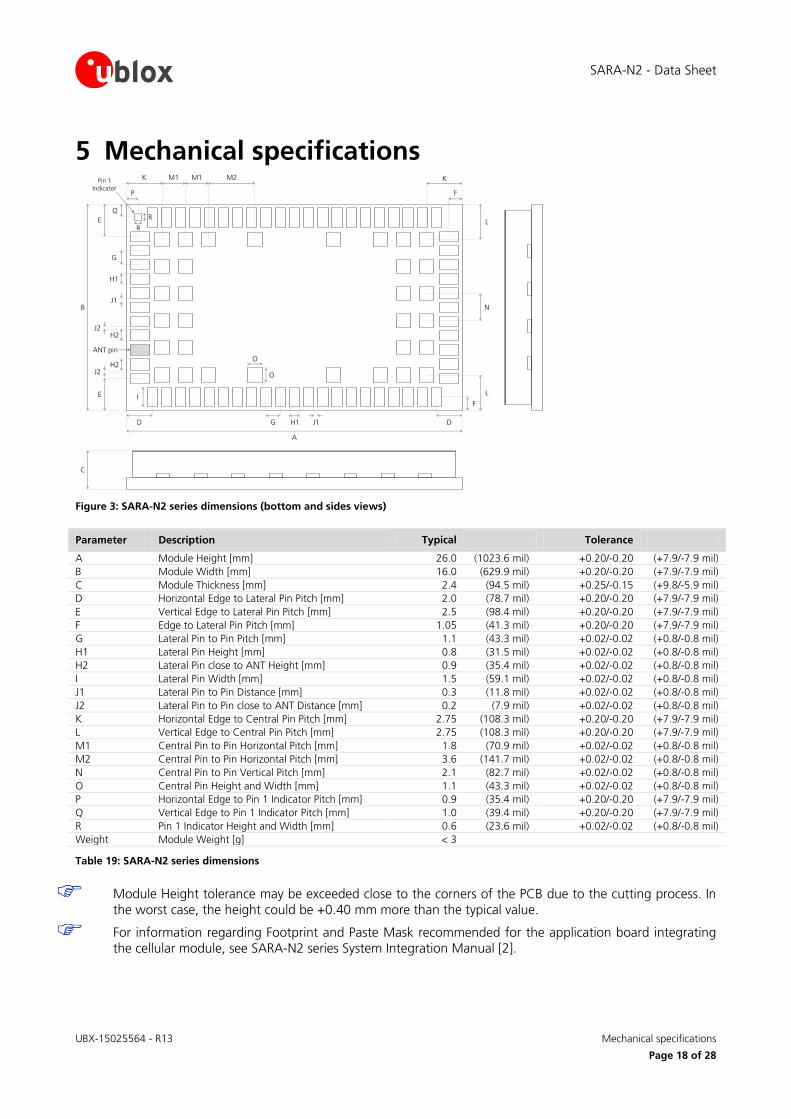
5 Mechanical specifications
C
R
R
P
Q
K M1 M1 M2
E
G
H1
J1
H2J2
J2H2
E
ANT pin
B
Pin 1 Indicator
K
G H1 J1
A
D D
O
O
L
N
LI
F
F
Figure 3: SARA-N2 series dimensions (bottom and sides views)
Parameter Description Typical Tolerance
A Module Height [mm] 26.0 (1023.6 mil) +0.20/-0.20 (+7.9/-7.9 mil)
B Module Width [mm] 16.0 (629.9 mil) +0.20/-0.20 (+7.9/-7.9 mil)
C Module Thickness [mm] 2.4 (94.5 mil) +0.25/-0.15 (+9.8/-5.9 mil)
D Horizontal Edge to Lateral Pin Pitch [mm] 2.0 (78.7 mil) +0.20/-0.20 (+7.9/-7.9 mil)
E Vertical Edge to Lateral Pin Pitch [mm] 2.5 (98.4 mil) +0.20/-0.20 (+7.9/-7.9 mil)
F Edge to Lateral Pin Pitch [mm] 1.05 (41.3 mil) +0.20/-0.20 (+7.9/-7.9 mil)
G Lateral Pin to Pin Pitch [mm] 1.1 (43.3 mil) +0.02/-0.02 (+0.8/-0.8 mil)
H1 Lateral Pin Height [mm] 0.8 (31.5 mil) +0.02/-0.02 (+0.8/-0.8 mil)
H2 Lateral Pin close to ANT Height [mm] 0.9 (35.4 mil) +0.02/-0.02 (+0.8/-0.8 mil)
I Lateral Pin Width [mm] 1.5 (59.1 mil) +0.02/-0.02 (+0.8/-0.8 mil)
J1 Lateral Pin to Pin Distance [mm] 0.3 (11.8 mil) +0.02/-0.02 (+0.8/-0.8 mil)
J2 Lateral Pin to Pin close to ANT Distance [mm] 0.2 (7.9 mil) +0.02/-0.02 (+0.8/-0.8 mil)
K Horizontal Edge to Central Pin Pitch [mm] 2.75 (108.3 mil) +0.20/-0.20 (+7.9/-7.9 mil)
L Vertical Edge to Central Pin Pitch [mm] 2.75 (108.3 mil) +0.20/-0.20 (+7.9/-7.9 mil)
M1 Central Pin to Pin Horizontal Pitch [mm] 1.8 (70.9 mil) +0.02/-0.02 (+0.8/-0.8 mil)
M2 Central Pin to Pin Horizontal Pitch [mm] 3.6 (141.7 mil) +0.02/-0.02 (+0.8/-0.8 mil)
N Central Pin to Pin Vertical Pitch [mm] 2.1 (82.7 mil) +0.02/-0.02 (+0.8/-0.8 mil)
O Central Pin Height and Width [mm] 1.1 (43.3 mil) +0.02/-0.02 (+0.8/-0.8 mil)
P Horizontal Edge to Pin 1 Indicator Pitch [mm] 0.9 (35.4 mil) +0.20/-0.20 (+7.9/-7.9 mil)
Q Vertical Edge to Pin 1 Indicator Pitch [mm] 1.0 (39.4 mil) +0.20/-0.20 (+7.9/-7.9 mil)
R Pin 1 Indicator Height and Width [mm] 0.6 (23.6 mil) +0.02/-0.02 (+0.8/-0.8 mil)
Weight Module Weight [g] < 3
Table 19: SARA-N2 series dimensions
Module Height tolerance may be exceeded close to the corners of the PCB due to the cutting process. In the worst case, the height could be +0.40 mm more than the typical value.
For information regarding Footprint and Paste Mask recommended for the application board integrating the cellular module, see SARA-N2 series System Integration Manual [2].
SARA-N2 - Data Sheet
UBX-15025564 - R13 Qualification and approvals
Page 19 of 28
6 Qualification and approvals
6.1 Reliability tests
Tests for product family qualifications are according to ISO 16750 “Road vehicles – Environmental conditions and testing for electrical and electronic equipment“, and appropriate standards.
6.2 Approvals
Products marked with this lead-free symbol on the product label comply with the “Directive 2002/95/EC of the European Parliament and the Council on the Restriction of Use of certain Hazardous Substances in Electrical and Electronic Equipment“ RoHS).
SARA-N2 series modules are RoHS compliant.
No natural rubbers, hygroscopic materials, or materials containing asbestos are employed.
Table 20 lists the main approvals for SARA-N2 series modules.
Certification Scheme SARA-N200 SARA-N201 SARA-N210 SARA-N211 SARA-N280
CE (European Conformity) • • •
GCF (Global Certification Forum) •
CCC (China Compulsory Certification) • •
SRRC (State Radio Regulation of China) • •
NCC (Taiwanese National Communications Commission) • • •
Anatel (Agência Nacional de Telecomunicações Brazil) •
RCM (Australia Regulatory Compliance Mark) •
NBTC (Thailand Regulatory Certification) •
IMDA (Singapore Regulatory Certification) •
ATEX (Atmosphere Explosive) •
China Telecom (Network Operator) •
China Unicom (Network Operator) •
Deutsche Telecom (Network Operator) • • •
Table 20: SARA-N2 series main certification approvals
For all the certificates of compliancy and for the complete list of approvals (including countries’ and network operators’ approvals) of SARA-N2 series modules, see our website (http://www.u-blox.com/) or please contact the u-blox office or sales representative nearest you.
SARA-N2 - Data Sheet
UBX-15025564 - R13 Qualification and approvals
Page 20 of 28
6.2.1 ATEX certification
SARA-N211 modules are certified as components intended for use in potentially explosive atmospheres compliant to the following standards:
IEC 60079-0
IEC 60079-11
IEC 60079-26
According to the standards listed above, the SARA-N211 modules are certified with the following marking:
Ex II 1G, Ex ia IIC
According to the marking stated above, the modules are certified as electrical equipment of:
group ‘II’: intended for use in areas with explosive gas atmosphere other than mines susceptible to firedamp
category ‘1G’: intended for use in zone 0 hazardous areas, in which explosive atmospheres caused by mixtures of air and gases, vapors or mists are present continuously, for long periods or frequently
level of protection ‘ia’: intrinsically safe apparatus with very high level of protection, not capable of causing ignition in normal operation and with the application of one countable fault or a combination of any two countable fault plus those non-countable faults which give the most onerous condition
subdivision ‘IIC’: intended for use in areas where the nature of the explosive gas atmosphere is considered very dangerous based on the Maximum Experimental Safe Gap or the Minimum Ignition Current ratio of the explosive gas atmosphere in which the equipment may be installed (a typical gas is hydrogen), so that the modules are also suitable for applications intended for use in subdivision IIB (typical gas is ethylene) and subdivision IIA (a typical gas is propane)
Section 4.2.1 defines the temperature range of use for SARA-N211 modules.
The RF radiating profile of SARA-N211 modules is compliant to all the applicable 3GPP / ETSI standards, with a maximum of 250 mW RF average power according to the LTE Cat NB1 Power Class stated in Table 2. Section 8.1 describes the nameplate of SARA-N211 modules (see Figure 7).
Table 21 lists the maximum input and equivalent parameters that must be considered in the sub-division IIC, the sub-division IIB and the sub-division IIA for SARA-N211 modules.
Parameter SARA-N211
Ui 4.2 V
Ii 0.5 A
Ci 68.1 µF
Li 8.5 µH
Table 21: Maximum input and equivalent parameters for sub-division IIC, IIB and IIA
For more information about the integration of these modules in applications intended for use in potentially explosive atmospheres, see the SARA-N2 Series System Integration Manual [2].
SARA-N2 - Data Sheet
UBX-15025564 - R13 Product handling
Page 21 of 28
7 Product handling
7.1 Packaging
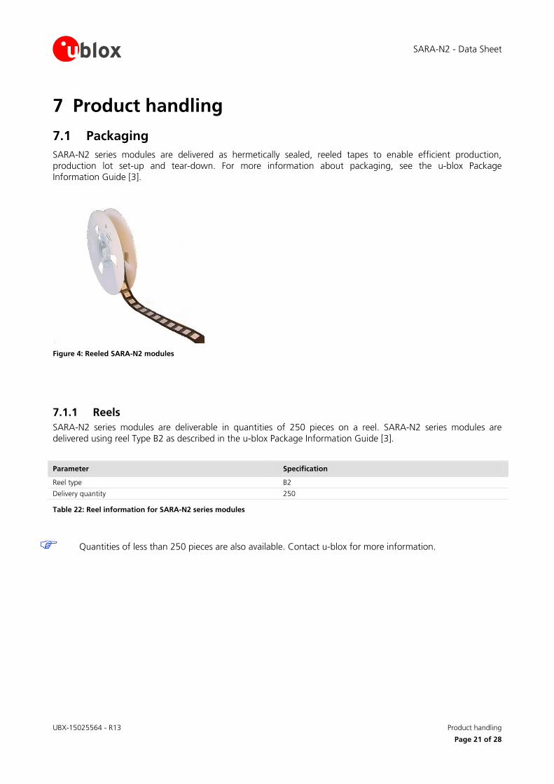
SARA-N2 series modules are delivered as hermetically sealed, reeled tapes to enable efficient production, production lot set-up and tear-down. For more information about packaging, see the u-blox Package Information Guide [3].
Figure 4: Reeled SARA-N2 modules
7.1.1 Reels
SARA-N2 series modules are deliverable in quantities of 250 pieces on a reel. SARA-N2 series modules are delivered using reel Type B2 as described in the u-blox Package Information Guide [3].
Parameter Specification
Reel type B2
Delivery quantity 250
Table 22: Reel information for SARA-N2 series modules
Quantities of less than 250 pieces are also available. Contact u-blox for more information.
SARA-N2 - Data Sheet
UBX-15025564 - R13 Product handling
Page 22 of 28
7.1.2 Tapes
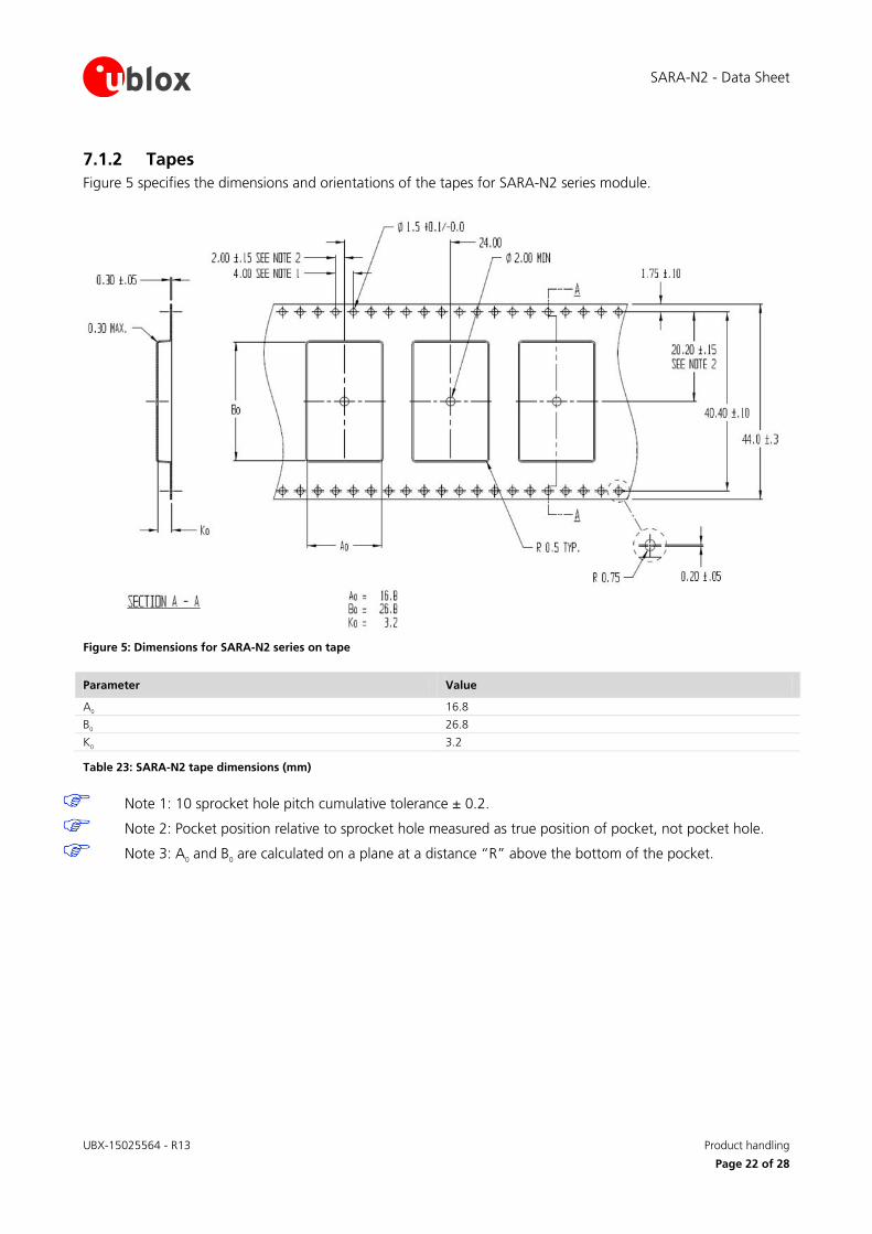
Figure 5 specifies the dimensions and orientations of the tapes for SARA-N2 series module.
Figure 5: Dimensions for SARA-N2 series on tape
Parameter Value
A0 16.8
B0 26.8
K0 3.2
Table 23: SARA-N2 tape dimensions (mm)
Note 1: 10 sprocket hole pitch cumulative tolerance ± 0.2.
Note 2: Pocket position relative to sprocket hole measured as true position of pocket, not pocket hole.
Note 3: A0 and B
0 are calculated on a plane at a distance “R” above the bottom of the pocket.

SARA-N2 - Data Sheet
UBX-15025564 - R13 Product handling
Page 23 of 28
7.2 Moisture Sensitivity Levels
SARA-N2 modules are Moisture Sensitive Devices (MSD) in accordance to IPC/JEDEC specification
The Moisture Sensitivity Level (MSL) relates to the packaging and handling precautions required. SARA-N2 modules are rated at MSL level 4. For more information regarding moisture sensitivity levels, labeling, storage and drying see the u-blox Package Information Guide [3].
For MSL standard see IPC/JEDEC J-STD-020 (can be downloaded from www.jedec.org).
7.3 Reflow soldering
Reflow profiles are to be selected according to u-blox recommendations (see SARA-N2 series System Integration Manual [2]).
Failure to observe these recommendations can result in severe damage to the device!
7.4 ESD precautions
SARA-N2 modules contain highly sensitive electronic circuitry and are Electrostatic Sensitive Devices (ESD). Handling SARA-N2 modules without proper ESD protection may destroy or damage them permanently.
SARA-N2 modules are Electrostatic Sensitive Devices (ESD) and require special ESD precautions typically applied to ESD sensitive components.
Table 7 reports the maximum ESD ratings of the SARA-N2 modules.
Proper ESD handling and packaging procedures must be applied throughout the processing, handling and operation of any application that incorporates SARA-N2 module.
ESD precautions should be implemented on the application board where the module is mounted, as described in the SARA-N2 series System Integration Manual [2].
Failure to observe these recommendations can result in severe damage to the device!

SARA-N2 - Data Sheet
UBX-15025564 - R13 Labeling and ordering information
Page 24 of 28
8 Labeling and ordering information
8.1 Product labeling
SARA-N2 module labels include important product information. Figure 6Figure 6 illustrates the label of all the SARA-N2 series modules except for SARA-N211 and includes: u-blox logo, production lot, Pb-free marking, product type number, module IMEI number, regulatory certification info, and production country.
xxB-xx
xxB-xx xxB-xx
xxB-xx
SARA-N200 SARA-N201
SARA-N210 SARA-N280
Figure 6 Location of product type number on SARA-N2 series module label
Figure 7 illustrates the label of SARA-N211 modules and includes: u-blox logo, production lot, Pb-free marking, product type number, IMEI number, ATEX marking with the IECEx and ATEX certificate numbers and category classification.
xxX-xx
IECEx SIQ XX.XXXXU
SIQ XX ATEX XXX U
II 1G Ex ia IIC
SARA-N211
1304
Figure 7: SARA-N211 module label
SARA-N2 - Data Sheet
UBX-15025564 - R13 Labeling and ordering information
Page 25 of 28
8.2 Explanation of codes
Three different product code formats are used. The Product Name is used in documentation such as this data sheet and identifies all u-blox products, independent of packaging and quality grade. The Ordering Code includes options and quality, while the Type Number includes the hardware and firmware versions. Table 24 below details these three different formats:
Format Structure
Product Name SARA-TGVV
Ordering Code SARA-TGVV-MMQ
Type Number SARA-TGVV-MMQ-XX
Table 24: Product code formats
Table 25 explains the parts of the product code.
Code Meaning Example
TG Platform (Technology and Generation):
Dominant technology (G: GSM; U: HSUPA; C: CDMA 1xRTT; N: NB-IoT; R: LTE low data rate (Cat 1 and below); L: LTE high data rate (Cat 3 and above))
Generation: 1…9
N2
VV Variant function set based on the same platform [00…99] 00
MM Major product version [00…99] 02
Q Product grade:
B = professional
A = automotive
X = ATEX certified
B
XX Minor product version (not relevant for certification) 00
Table 25: Part identification code
8.3 Ordering codes
Ordering No. Product
SARA-N200-02B Narrowband IoT module supporting Band 8, mainly designed for operation in Europe / APAC
26.0 x 16.0 x 2.4 mm, 250 pcs/reel
SARA-N201-02B Narrowband IoT module supporting Band 5, mainly designed for operation in APAC
26.0 x 16.0 x 2.4 mm, 250 pcs/reel
SARA-N210-02B Narrowband IoT module supporting Band 20, mainly designed for operation in Europe
26.0 x 16.0 x 2.4 mm, 250 pcs/reel
SARA-N211-02X Narrowband IoT module supporting Band 8 and 20, mainly designed for operation in Europe
ATEX certified
26.0 x 16.0 x 2.4 mm, 250 pcs/reel
SARA-N280-02B Narrowband IoT module supporting Band 28, mainly designed for operation in South America / APAC
26.0 x 16.0 x 2.4 mm, 250 pcs/reel
Table 26: Product ordering codes
Product changes affecting form, fit or function are documented by u-blox. For a list of Product Change Notifications (PCNs) see our website.

SARA-N2 - Data Sheet
UBX-15025564 - R13 Appendix
Page 26 of 28
Appendix
A Glossary Name Definition
ADC Analog to Digital Converter
DDC Display Data Channel (I2C compatible) Interface
DL Down-link (Reception)
ERS External Reset Input Signal
GDI Generic Digital Interfaces (power domain)
GND Ground
GNSS Global Navigation Satellite System
GPIO General Purpose Input Output
GSM Global System for Mobile Communication
GMSK Gaussian Minimum Shift Keying
I2C Inter-Integrated Circuit Interface
LGA Land Grid Array
PCN Product Change Notification / Information Note / Sample Delivery Note
PSK Phase Shift Keying
NB-IoT Narrow Band – Internet of Things
SIM Subscriber Identity Module
SPI Serial Peripheral Interface
TBD To Be Defined
UART Universal Asynchronous Receiver-Transmitter serial interface
UL Up-link (Transmission)
Table 27: Explanation of abbreviations and terms used
SARA-N2 - Data Sheet
UBX-15025564 - R13 Related documents
Page 27 of 28
Related documents [1] u-blox SARA-N2 series AT Commands Manual, Docu No UBX-16014887
[2] u-blox SARA-N2 series System Integration Manual, Docu No UBX-17005143
[3] u-blox Package Information Guide, Docu No UBX-14001652
For regular updates to u-blox documentation and to receive product change notifications please register on our homepage.
Revision history
Revision Date Name Comments
R01 09-Dec-2015 sfal Initial release
R02 23-Feb-2016 sfal Document aligned with features supported by the first FW delivery. AT command section
added
R03 15-Apr-2016 sfal Document aligned with features supported by FW V100R100C00B100
R04 20-Jun-2016 sfal Voltage extended operating range values added. AT commands section removed
R05 31-Oct-2016 sfal Document updated to product version "01"
R06 13-Dec-2016 sfal Added additional requirements on the secondary UART. Updates on data rates, secondary
UART baud rate and supported features.
R07 22-Feb-2017 sfal Extended document applicability to SARA-N280-01B. Changed UL/DL data rates
R08 24-Mar-2017 sfal Document applicability extended to product version "02" and added SARA-N200-02B. Removed SPI interface (not supported)
R09 22-May-2017 sfal / sses Document updated for Prototypes of "02"product version
R10 01-Aug-2017 sfal / lpah Updated disclaimer restriction
Updated product status for "01B" product version
Updated current consumption in Rx mode
R11 09-Oct-2017 sses Updated VCC, V_INT, RESET_N and GPIO description
Updated main certification approvals
R12 17-Oct-2017 lpah ES application version updated
R13 22-Feb-2018 lpah / sses Extended document applicability to SARA-N211-02X and updated product status.
Updated VCC supply extended operating voltage range
Updated Antenna Detection, GPIO, approvals, and labels section
SARA-N2 - Data Sheet
UBX-15025564 - R13 Contact
Page 28 of 28
Contact For complete contact information visit us at www.u-blox.com
u-blox Offices
North, Central and South America
u-blox America, Inc.
Phone: +1 703 483 3180 E-mail: [email protected]
Regional Office West Coast:
Phone: +1 408 573 3640 E-mail: [email protected]
Technical Support:
Phone: +1 703 483 3185 E-mail: [email protected]
Headquarters Europe, Middle East, Africa
u-blox AG
Phone: +41 44 722 74 44 E-mail: [email protected] Support: [email protected]
Asia, Australia, Pacific
u-blox Singapore Pte. Ltd.
Phone: +65 6734 3811 E-mail: [email protected] Support: [email protected]
Regional Office Australia:
Phone: +61 2 8448 2016 E-mail: [email protected] Support: [email protected]
Regional Office China (Beijing):
Phone: +86 10 68 133 545 E-mail: [email protected] Support: [email protected]
Regional Office China (Chongqing):
Phone: +86 23 6815 1588 E-mail: [email protected] Support: [email protected]
Regional Office China (Shanghai):
Phone: +86 21 6090 4832 E-mail: [email protected] Support: [email protected]
Regional Office China (Shenzhen):
Phone: +86 755 8627 1083 E-mail: [email protected] Support: [email protected]
Regional Office India:
Phone: +91 80 4050 9200 E-mail: [email protected] Support: [email protected]
Regional Office Japan (Osaka):
Phone: +81 6 6941 3660 E-mail: [email protected] Support: [email protected]
Regional Office Japan (Tokyo):
Phone: +81 3 5775 3850 E-mail: [email protected] Support: [email protected]
Regional Office Korea:
Phone: +82 2 542 0861 E-mail: [email protected] Support: [email protected]
Regional Office Taiwan:
Phone: +886 2 2657 1090 E-mail: [email protected] Support: [email protected]