sbas267 – march 2003 precision analog-to-digital converter ... · precision analog-to-digital...
TRANSCRIPT

MSC1211
SBAS267 – MARCH 2003
www.ti.com
FEATURESANALOG FEATURES
24-BITS NO MISSING CODES 22-BITS EFFECTIVE RESOLUTION AT 10Hz
Low Noise: 75nV PGA FROM 1 TO 128 PRECISION ON-CHIP VOLTAGE REFERENCE:
Accuracy: 0.2%Drift: 5ppm/°C
8 DIFFERENTIAL/SINGLE-ENDED CHANNELS ON-CHIP OFFSET/GAIN CALIBRATION OFFSET DRIFT: 0.02PPM/°C GAIN DRIFT: 0.5PPM/°C ON-CHIP TEMPERATURE SENSOR SELECTABLE BUFFER INPUT BURNOUT DETECT QUAD 16-BIT MONOTONIC VOLTAGE DACs:
2 VDACs Can Be Programmed as IDACs8µs Settling Time
DIGITAL FEATURES
Microcontroller Core
8051 COMPATIBLE HIGH SPEED CORE:
4 Clocks per Instruction Cycle DC TO 30MHz SINGLE INSTRUCTION 133ns DUAL DATA POINTER
Memory
UP TO 32kB FLASH DATA MEMORY FLASH MEMORY PARTITIONING ENDURANCE 1M ERASE/WRITE CYCLES,
100 YEAR DATA RETENTION IN-SYSTEM SERIALLY PROGRAMMABLE EXTERNAL PROGRAM/DATA MEMORY (64kB) 1280 BYTES DATA SRAM FLASH MEMORY SECURITY 2kB BOOT ROM PROGRAMMABLE WAIT STATE CONTROL
Copyright © 2003, Texas Instruments Incorporated
Precision Analog-to-Digital Converter (ADC)and Digital-to-Analog Converters (DACs)
with 8051 Microcontroller and Flash Memory
MSC1211®
Please be aware that an important notice concerning availability, standard warranty, and use in critical applications ofTexas Instruments semiconductor products and disclaimers thereto appears at the end of this data sheet.
All trademarks are the property of their respective owners.
Peripheral Features
34 I/O PINS ADDITIONAL 32-BIT ACCUMULATOR THREE 16-BIT TIMER/COUNTERS SYSTEM TIMERS PROGRAMMABLE WATCHDOG TIMER FULL DUPLEX DUAL UART MASTER/SLAVE SPI™ WITH DMA MULTI-MASTER I2C™ 16-BIT PWM POWER MANAGEMENT CONTROL INTERNAL CLOCK DIVIDER IDLE MODE CURRENT < 200µA STOP MODE CURRENT < 100nA PROGRAMMABLE BROWNOUT RESET PROGRAMMABLE LOW VOLTAGE DETECT 21 INTERRUPT SOURCES TWO HARDWARE BREAKPOINTS
GENERAL FEATURES
PIN COMPATIBLE WITH MSC1210 FAMILY PACKAGE: TQFP-64 LOW POWER: 4mW INDUSTRIAL TEMPERATURE RANGE:
–40°C to +85°C POWER SUPPLY: 2.7V to 5.25V
APPLICATIONS INDUSTRIAL PROCESS CONTROL INSTRUMENTATION LIQUID/GAS CHROMATOGRAPHY BLOOD ANALYSIS SMART TRANSMITTERS PORTABLE INSTRUMENTS WEIGH SCALES PRESSURE TRANSDUCERS INTELLIGENT SENSORS PORTABLE APPLICATIONS DAS SYSTEMS
PRODUCTION DATA information is current as of publication date.Products conform to specifications per the terms of Texas Instrumentsstandard warranty. Production processing does not necessarily includetesting of all parameters.

MSC12112SBAS267www.ti.com
PACKAGE/ORDERING INFORMATIONSPECIFIED
FLASH PACKAGE TEMPERATURE PACKAGE ORDERING TRANSPORTPRODUCT MEMORY PACKAGE-LEAD DESIGNATOR(1) RANGE MARKING NUMBER MEDIA, QUANTITY
MSC1211Y2 4k TQFP-64 PAG –40°C to +85°C MSC1211Y2 MSC1211Y2PAGT Tape and Reel, 250MSC1211Y2 4k " " " " MSC1211Y2PAGR Tape and Reel, 2000
MSC1211Y3 8k TQFP-64 PAG –40°C to +85°C MSC1211Y3 MSC1211Y3PAGT Tape and Reel, 250MSC1211Y3 8k " " " " MSC1211Y3PAGR Tape and Reel, 2000
MSC1211Y4 16k TQFP-64 PAG –40°C to +85°C MSC1211Y4 MSC1211Y4PAGT Tape and Reel, 250MSC1211Y4 16k " " " " MSC1211Y4PAGR Tape and Reel, 2000
MSC1211Y5 32k TQFP-64 PAG –40°C to +85°C MSC1211Y5 MSC1211Y5PAGT Tape and Reel, 250MSC1211Y5 32k " " " " MSC1211Y5PAGR Tape and Reel, 2000
NOTE: (1) For the most current specifications and package information, refer to our web site at www.ti.com/msc.
ABSOLUTE MAXIMUM RATINGS(1)
Analog InputsInput Current ............................................................ 100mA, MomentaryInput Current .............................................................. 10mA, ContinuousInput Voltage ............................................. AGND – 0.5V to AVDD + 0.5V
Power SupplyDVDD to DGND ...................................................................... –0.3V to 6VAVDD to AGND ...................................................................... –0.3V to 6VAGND to DGND .............................................................. –0.3V to +0.3VVREF to AGND ....................................................... –0.3V to AVDD + 0.3VDigital Input Voltage to DGND .............................. –0.3V to DVDD + 0.3VDigital Output Voltage to DGND ........................... –0.3V to DVDD + 0.3VMaximum Junction Temperature ................................................ +150°COperating Temperature Range ...................................... –40°C to +85°CStorage Temperature Range ....................................... –65°C to +150°CLead Temperature (soldering, 10s) ............................................ +300°CPackage Power Dissipation ........................................................ 900mWOutput Current All Pins ................................................................ 200mAOutput Pin Short Circuit ..................................................................... 10sThermal Resistance, Junction-to-Ambient (θJA) ....................... 66.6°C/WThermal Resistance, Junction-to-Case (θJC) ............................. 4.3°C/W
Digital OutputsOutput Current ......................................................... 100mA, ContinuousI/O Source/Sink Current ............................................................... 100mAPower Pin Maximum .................................................................... 300mA
NOTE: (1) Stresses beyond those listed under “Absolute Maximum Ratings”may cause permanent damage to the device. Exposure to absolute-maximum-rated conditions for extended periods may affect device reliability.
ELECTROSTATICDISCHARGE SENSITIVITY
This integrated circuit can be damaged by ESD. TexasInstruments recommends that all integrated circuits be handledwith appropriate precautions. Failure to observe proper han-dling and installation procedures can cause damage.
ESD damage can range from subtle performance degrada-tion to complete device failure. Precision integrated circuitsmay be more susceptible to damage because very smallparametric changes could cause the device not to meet itspublished specifications.
FEATURES(1) MSC1211Y2(2) MSC1211Y3(2) MSC1211Y4(2) MSC1211Y5(2)
Flash Program Memory (Bytes) Up to 4k Up to 8k Up to 16k Up to 32kFlash Data Memory (Bytes) Up to 4k Up to 8k Up to 16k Up to 32kInternal Scratchpad RAM (Bytes) 256 256 256 256Internal MOVX SRAM (Bytes) 1024 1024 1024 1024Externally Accessible Memory (Bytes) 64k Program, 64k Data 64k Program, 64k Data 64k Program, 64k Data 64k Program, 64k Data
NOTES: (1) All peripheral features are the same on all devices; the flash memory size is the only difference. (2) The last digit of the part number (N) representsthe onboard flash size = (2N)kBytes.
MSC1211YX FAMILY FEATURES
MSC1211 3SBAS267 www.ti.com
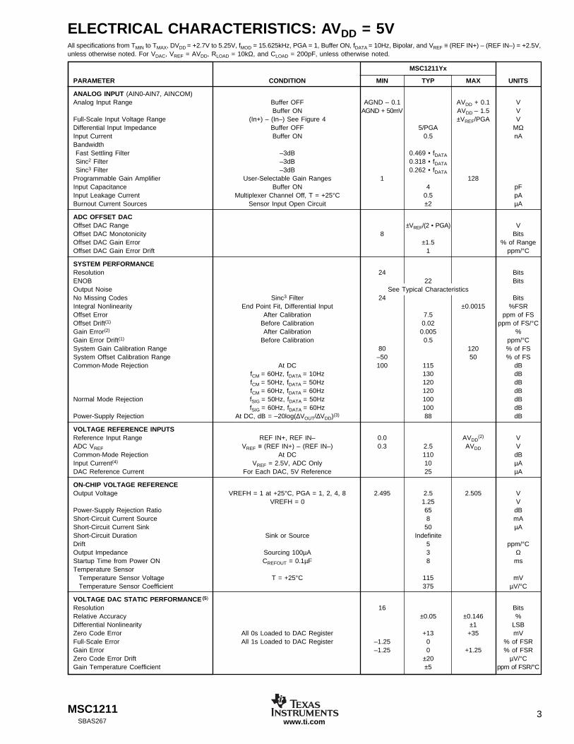
ELECTRICAL CHARACTERISTICS: AVDD = 5VAll specifications from TMIN to TMAX, DVDD = +2.7V to 5.25V, fMOD = 15.625kHz, PGA = 1, Buffer ON, fDATA = 10Hz, Bipolar, and VREF ≡ (REF IN+) – (REF IN–) = +2.5V,unless otherwise noted. For VDAC, VREF = AVDD, RLOAD = 10kΩ, and CLOAD = 200pF, unless otherwise noted.
MSC1211Yx
PARAMETER CONDITION MIN TYP MAX UNITS
ANALOG INPUT (AIN0-AIN7, AINCOM)Analog Input Range Buffer OFF AGND – 0.1 AVDD + 0.1 V
Buffer ON AGND + 50mV AVDD – 1.5 VFull-Scale Input Voltage Range (In+) – (In–) See Figure 4 ±VREF/PGA VDifferential Input Impedance Buffer OFF 5/PGA MΩInput Current Buffer ON 0.5 nABandwidth Fast Settling Filter –3dB 0.469 • fDATA
Sinc2 Filter –3dB 0.318 • fDATA
Sinc3 Filter –3dB 0.262 • fDATA
Programmable Gain Amplifier User-Selectable Gain Ranges 1 128Input Capacitance Buffer ON 4 pFInput Leakage Current Multiplexer Channel Off, T = +25°C 0.5 pABurnout Current Sources Sensor Input Open Circuit ±2 µA
ADC OFFSET DACOffset DAC Range ±VREF/(2 • PGA) VOffset DAC Monotonicity 8 BitsOffset DAC Gain Error ±1.5 % of RangeOffset DAC Gain Error Drift 1 ppm/°C
SYSTEM PERFORMANCEResolution 24 BitsENOB 22 BitsOutput Noise See Typical CharacteristicsNo Missing Codes Sinc3 Filter 24 BitsIntegral Nonlinearity End Point Fit, Differential Input ±0.0015 %FSROffset Error After Calibration 7.5 ppm of FSOffset Drift(1) Before Calibration 0.02 ppm of FS/°CGain Error(2) After Calibration 0.005 %Gain Error Drift(1) Before Calibration 0.5 ppm/°CSystem Gain Calibration Range 80 120 % of FSSystem Offset Calibration Range –50 50 % of FSCommon-Mode Rejection At DC 100 115 dB
fCM = 60Hz, fDATA = 10Hz 130 dBfCM = 50Hz, fDATA = 50Hz 120 dBfCM = 60Hz, fDATA = 60Hz 120 dB
Normal Mode Rejection fSIG = 50Hz, fDATA = 50Hz 100 dBfSIG = 60Hz, fDATA = 60Hz 100 dB
Power-Supply Rejection At DC, dB = –20log(∆VOUT/∆VDD)(3) 88 dB
VOLTAGE REFERENCE INPUTSReference Input Range REF IN+, REF IN– 0.0 AVDD
(2) VADC VREF VREF ≡ (REF IN+) – (REF IN–) 0.3 2.5 AVDD VCommon-Mode Rejection At DC 110 dBInput Current(4) VREF = 2.5V, ADC Only 10 µADAC Reference Current For Each DAC, 5V Reference 25 µA
ON-CHIP VOLTAGE REFERENCEOutput Voltage VREFH = 1 at +25°C, PGA = 1, 2, 4, 8 2.495 2.5 2.505 V
VREFH = 0 1.25 VPower-Supply Rejection Ratio 65 dBShort-Circuit Current Source 8 mAShort-Circuit Current Sink 50 µAShort-Circuit Duration Sink or Source IndefiniteDrift 5 ppm/°COutput Impedance Sourcing 100µA 3 ΩStartup Time from Power ON CREFOUT = 0.1µF 8 msTemperature Sensor
Temperature Sensor Voltage T = +25°C 115 mVTemperature Sensor Coefficient 375 µV/°C
VOLTAGE DAC STATIC PERFORMANCE (5)
Resolution 16 BitsRelative Accuracy ±0.05 ±0.146 %Differential Nonlinearity ±1 LSBZero Code Error All 0s Loaded to DAC Register +13 +35 mVFull-Scale Error All 1s Loaded to DAC Register –1.25 0 % of FSRGain Error –1.25 0 +1.25 % of FSRZero Code Error Drift ±20 µV/°CGain Temperature Coefficient ±5 ppm of FSR/°C
MSC12114SBAS267www.ti.com
ELECTRICAL CHARACTERISTICS: AVDD = 3VAll specifications from TMIN to TMAX, AVDD = +3V, DVDD = +2.7V to 5.25V, fMOD = 15.625kHz, PGA = 1, Buffer ON, fDATA = 10Hz, Bipolar, and VREF ≡ (REF IN+) – (REF IN–) = +1.25V,unless otherwise noted. For VDAC, VREF = AVDD, RLOAD = 10kΩ, and CLOAD = 200pF, unless otherwise noted.
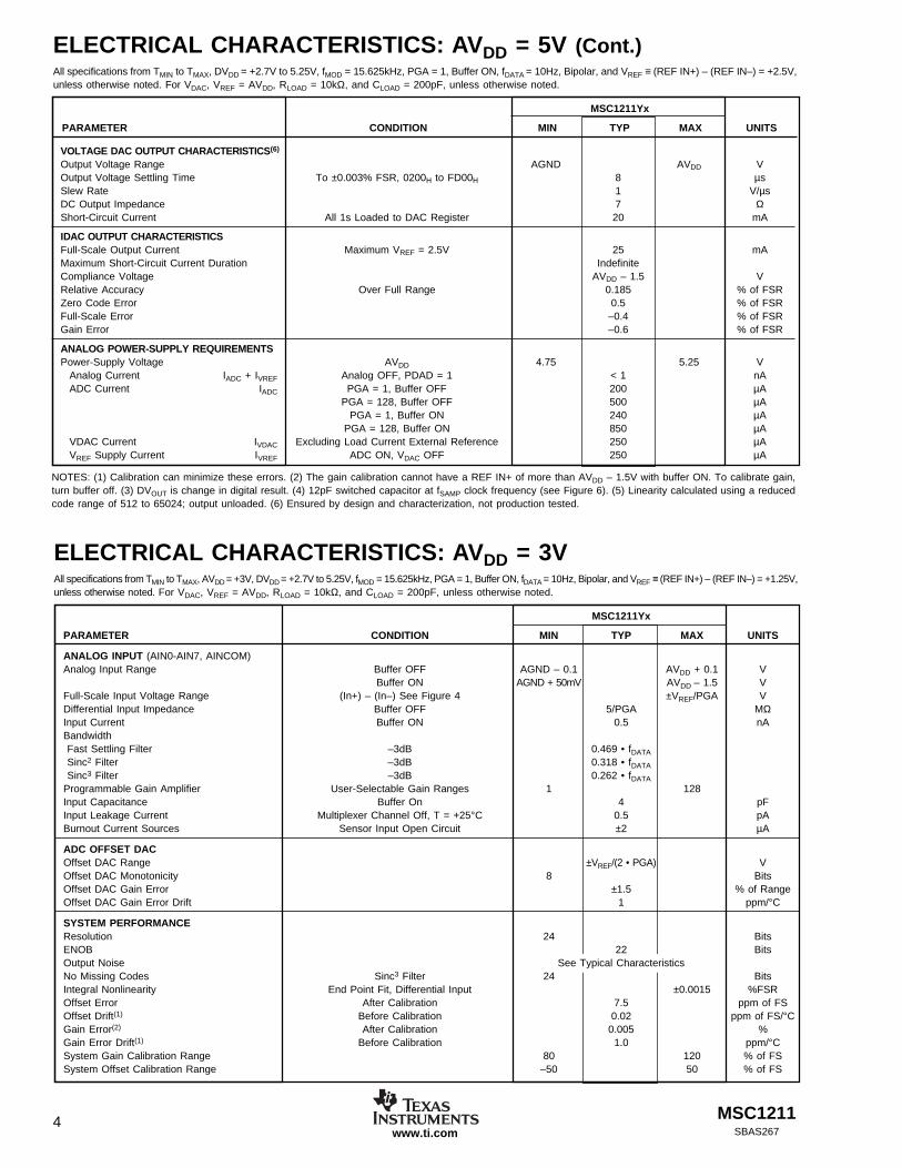
ELECTRICAL CHARACTERISTICS: AVDD = 5V (Cont.)All specifications from TMIN to TMAX, DVDD = +2.7V to 5.25V, fMOD = 15.625kHz, PGA = 1, Buffer ON, fDATA = 10Hz, Bipolar, and VREF ≡ (REF IN+) – (REF IN–) = +2.5V,unless otherwise noted. For VDAC, VREF = AVDD, RLOAD = 10kΩ, and CLOAD = 200pF, unless otherwise noted.
MSC1211Yx
PARAMETER CONDITION MIN TYP MAX UNITS
VOLTAGE DAC OUTPUT CHARACTERISTICS(6)
Output Voltage Range AGND AVDD VOutput Voltage Settling Time To ±0.003% FSR, 0200H to FD00H 8 µsSlew Rate 1 V/µsDC Output Impedance 7 ΩShort-Circuit Current All 1s Loaded to DAC Register 20 mA
IDAC OUTPUT CHARACTERISTICSFull-Scale Output Current Maximum VREF = 2.5V 25 mAMaximum Short-Circuit Current Duration IndefiniteCompliance Voltage AVDD – 1.5 VRelative Accuracy Over Full Range 0.185 % of FSRZero Code Error 0.5 % of FSRFull-Scale Error –0.4 % of FSRGain Error –0.6 % of FSR
ANALOG POWER-SUPPLY REQUIREMENTSPower-Supply Voltage AVDD 4.75 5.25 V
Analog Current IADC + IVREF Analog OFF, PDAD = 1 < 1 nAADC Current IADC PGA = 1, Buffer OFF 200 µA
PGA = 128, Buffer OFF 500 µAPGA = 1, Buffer ON 240 µA
PGA = 128, Buffer ON 850 µAVDAC Current IVDAC Excluding Load Current External Reference 250 µAVREF Supply Current IVREF ADC ON, VDAC OFF 250 µA
NOTES: (1) Calibration can minimize these errors. (2) The gain calibration cannot have a REF IN+ of more than AVDD – 1.5V with buffer ON. To calibrate gain,turn buffer off. (3) DVOUT is change in digital result. (4) 12pF switched capacitor at fSAMP clock frequency (see Figure 6). (5) Linearity calculated using a reducedcode range of 512 to 65024; output unloaded. (6) Ensured by design and characterization, not production tested.
MSC1211Yx
PARAMETER CONDITION MIN TYP MAX UNITS
ANALOG INPUT (AIN0-AIN7, AINCOM)Analog Input Range Buffer OFF AGND – 0.1 AVDD + 0.1 V
Buffer ON AGND + 50mV AVDD – 1.5 VFull-Scale Input Voltage Range (In+) – (In–) See Figure 4 ±VREF/PGA VDifferential Input Impedance Buffer OFF 5/PGA MΩInput Current Buffer ON 0.5 nABandwidth Fast Settling Filter –3dB 0.469 • fDATA
Sinc2 Filter –3dB 0.318 • fDATA
Sinc3 Filter –3dB 0.262 • fDATA
Programmable Gain Amplifier User-Selectable Gain Ranges 1 128Input Capacitance Buffer On 4 pFInput Leakage Current Multiplexer Channel Off, T = +25°C 0.5 pABurnout Current Sources Sensor Input Open Circuit ±2 µA
ADC OFFSET DACOffset DAC Range ±VREF/(2 • PGA) VOffset DAC Monotonicity 8 BitsOffset DAC Gain Error ±1.5 % of RangeOffset DAC Gain Error Drift 1 ppm/°C
SYSTEM PERFORMANCEResolution 24 BitsENOB 22 BitsOutput Noise See Typical CharacteristicsNo Missing Codes Sinc3 Filter 24 BitsIntegral Nonlinearity End Point Fit, Differential Input ±0.0015 %FSROffset Error After Calibration 7.5 ppm of FSOffset Drift(1) Before Calibration 0.02 ppm of FS/°CGain Error(2) After Calibration 0.005 %Gain Error Drift(1) Before Calibration 1.0 ppm/°CSystem Gain Calibration Range 80 120 % of FSSystem Offset Calibration Range –50 50 % of FS

MSC1211 5SBAS267 www.ti.com
ELECTRICAL CHARACTERISTICS: AVDD = 3V (Cont.)All specifications from TMIN to TMAX, AVDD = +3V, DVDD = +2.7V to 5.25V, fMOD = 15.625kHz, PGA = 1, Buffer ON, fDATA = 10Hz, and Bipolar, VREF ≡ (REF IN+) – (REF IN–) = +1.25V,unless otherwise noted. For VDAC, VREF = AVDD, RLOAD = 10kΩ, and CLOAD = 200pF, unless otherwise noted.
MSC1211Yx
PARAMETER CONDITION MIN TYP MAX UNITS
SYSTEM PERFORMANCE (Cont.)Common-Mode Rejection At DC 100 115 dB
fCM = 60Hz, fDATA = 10Hz 130 dBfCM = 50Hz, fDATA = 50Hz 120 dBfCM = 60Hz, fDATA = 60Hz 120 dB
Normal Mode Rejection fSIG = 50Hz, fDATA = 50Hz 100 dBfSIG = 60Hz, fDATA = 60Hz 100 dB
Power-Supply Rejection At DC, dB = –20log(DVOUT/DVDD)(3) 85 dB
VOLTAGE REFERENCE INPUTSReference Input Range REF IN+, REF IN– 0.0 AVDD
(2) VADC VREF VREF ≡ (REF IN+) – (REF IN–) 0.3 1.25 AVDD VCommon-Mode Rejection At DC 110 dBInput Current(4) VREF = 1.25V, ADC Only 10 µADAC Reference Current For each DAC, 3V Reference 25 µA
ON-CHIP VOLTAGE REFERENCEOutput Voltage VREFH = 0 at +25°C, PGA = 1, 2, 4, 8 1.245 1.25 1.255 VPower-Supply Rejection Ratio 65 dBShort-Circuit Current Source 2.6 mAShort-Circuit Current Sink 50 µAShort-Circuit Duration Sink or Source IndefiniteDrift 5 ppm/°COutput Impedance Sourcing 100µA 3 ΩStartup Time from Power ON CREFOUT = 0.1µF 8 msTemperature Sensor
Temperature Sensor Voltage T = +25°C 115 mVTemperature Sensor Coefficient 375 µV/°C
VOLTAGE DAC STATIC PERFORMANCE (5)
Resolution 16 BitsRelative Accuracy ±0.05 ±0.146 % of FSRDifferential Nonlinearity Ensured Monotonic by Design ±1 LSBZero Code Error All 0s Loaded to DAC Register +13 +35 mVFull-Scale Error All 1s Loaded to DAC Register –1.25 0 % of FSRGain Error –1.25 0 ±1.25 % of FSRZero Code Error Drift ±20 µV/°CGain Temperature Coefficient ±5 ppm of FSR/°C
VOLTAGE DAC OUTPUT CHARACTERISTICS(6)
Output Voltage Range AGND AVDD VOutput Voltage Settling Time To ±0.003% FSR, 0200H to FD00H 8 µsSlew Rate 1 V/µsDC Output Impedance 7 ΩShort-Circuit Current All 1s Loaded to DAC Register 16 mA
IDAC OUTPUT CHARACTERISTICSFull-Scale Output Current Maximum VREF = 2.5V 25 mAMaximum Short-Circuit Current Duration IndefiniteCompliance Voltage AVDD – 1.5Relative Accuracy Over Full Range 0.185 % of FSRZero Code Error 0.5 % of FSRFull-Scale Error –0.4 % of FSRGain Error –0.6 % of FSR
POWER-SUPPLY REQUIREMENTSPower-Supply Voltage AVDD 2.7 3.6 V Analog Current IADC + IVREF Analog OFF, PDAD = 1 < 1 nAADC Current IADC PGA = 1, Buffer OFF 200 µA
PGA = 128, Buffer OFF 500 µAPGA = 1, Buffer ON 240 µA
PGA = 128, Buffer ON 850 µAVDAC Current IVDAC Excluding Load Current External Reference 250 µAVREF Current IVREF 250 µA
NOTES: (1) Calibration can minimize these errors. (2) The gain calibration cannot have a REF IN+ of more than AVDD – 1.5V with buffer ON. To calibrate gain,turn buffer off. (3) DVOUT is change in digital result. (4) 12pF switched capacitor at fSAMP clock frequency (see Figure 6). (5) Linearity calculated using a reducedcode range of 512 to 65024; output unloaded. (6) Ensured by design and characterization, not production tested.
MSC12116SBAS267www.ti.com
DIGITAL CHARACTERISTICS: DVDD = 2.7V to 5.25VAll specifications from TMIN to TMAX, unless otherwise specified.
MSC1211Yx
PARAMETER CONDITION MIN TYP MAX UNITS
POWER-SUPPLY REQUIREMENTSDVDD 2.7 3.6 V
Normal Mode, fOSC = 1MHz 1.3 mANormal Mode, fOSC = 8MHz 6 mA
Stop Mode 100 nA
DVDD 4.75 5.25 VNormal Mode, fOSC = 1MHz 2.2 mANormal Mode, fOSC = 8MHz 14 mA
Stop Mode 100 nA
DIGITAL INPUT/OUTPUT (CMOS)Logic Level: VIH (except XIN pin) 0.6 • DVDD DVDD V
VIL (except XIN pin) DGND 0.2 • DVDD VPorts 0-3, Input Leakage Current, Input Mode VIH = DVDD or VIH = 0V –10 0 +10 µAPins EA, XIN Input Leakage Current 0 µAVOL, ALE, PSEN, Ports 0-3, All Output Modes IOL = 1mA DGND 0.4 VVOL, ALE, PSEN, Ports 0-3, All Output Modes IOL = 30mA, 3V (20mA) 1.5 VVOH, ALE, PSEN, Ports 0-3, Strong Drive Output IOH = 1mA DVDD – 0.4 DVDD – 0.1 DVDD VVOH, ALE, PSEN, Ports 0-3, Strong Drive Output IOH = 30mA, 3V (20mA) DVDD – 1.5 VPorts 0-3 Pull-Up Resistors 9 kΩPins ALE, PSEN, Pull-Up Resistors Flash Programming Mode Only 9 kΩPin RST, Pull-Down Resistor 200 kΩ
FLASH MEMORY CHARACTERISTICS: DVDD = 2.7V to 5.25VtUSEC = 1µs, tMSEC = 1ms
MSC1211Yx
PARAMETER CONDITION MIN TYP MAX UNITS
Flash Memory Endurance 100,000 1,000,000 cyclesFlash Memory Data Retention 100 YearsMass and Page Erase Time Set with FER Value in FTCON 10 msFlash Memory Data Retention Set with FWR Value in FTCON 30 40 µs

MSC1211 7SBAS267 www.ti.com
MD2 MD1 MD0 MOVX DURATION tMCS
0 0 0 2 Machine Cycles 0
0 0 1 3 Machine Cycles (default) 4tCLK
0 1 0 4 Machine Cycles 8tCLK
0 1 1 5 Machine Cycles 12tCLK
1 0 0 6 Machine Cycles 16tCLK
1 0 1 7 Machine Cycles 20tCLK
1 1 0 8 Machine Cycles 24tCLK
1 1 1 9 Machine Cycles 28tCLK
AC ELECTRICAL CHARACTERISTICS(1)(2): DVDD = 2.7V to 5.25V2.7V to 3.6V 4.75V to 5.25V
SYMBOL FIGURE PARAMETER MIN MAX MIN MAX UNITS
System ClockfOSC
(3) D External Crystal Frequency (fOSC) 1 16 1 30 MHz
1/tOSC(3) D External Clock Frequency (fOSC) 0 16 1 30 MHz
fOSC(3) D External Ceramic Resonator Frequency (fOSC) 1 12 1 12 MHz
Program MemorytLHLL A ALE Pulse Width 1.5tCLK – 5 1.5tCLK – 5 ns
tAVLL A Address Valid to ALE LOW 0.5tCLK – 10 0.5tCLK – 7 ns
tLLAX A Address Hold After ALE LOW 0.5tCLK 0.5tCLK ns
tLLIV A ALE LOW to Valid Instruction In 2.5tCLK – 35 2.5tCLK – 25 ns
tLLPL A ALE LOW to PSEN LOW 0.5tCLK 0.5tCLK ns
tPLPH A PSEN Pulse Width 2tCLK – 5 2tCLK – 5 ns
tPLIV A PSEN LOW to Valid Instruction In 2tCLK – 40 2tCLK – 30 ns
tPXIX A Input Instruction Hold After PSEN 5 –5 ns
tPXIZ A Input Instruction Float After PSEN tCLK – 5 tCLK ns
tAVIV A Address to Valid Instruction In 3tCLK – 40 3tCLK – 25 ns
tPLAZ A PSEN LOW to Address Float 0 0 ns
Data MemorytRLRH B RD Pulse Width (tMCS = 0)(4) 2tCLK – 5 2tCLK – 5 ns
B RD Pulse Width (tMCS > 0)(4) tMCS – 5 tMCS – 5 ns
tWLWH C WR Pulse Width (tMCS = 0)(4) 2tCLK – 5 2tCLK – 5 nsC Pulse Width (tMCS > 0)(4) tMCS – 5 tMCS – 5 ns
tRLDV B RD LOW to Valid Data In (tMCS = 0)(4) 2tCLK – 40 2tCLK – 30 nsB RD LOW to Valid Data In (tMCS > 0)(4) tMCS – 40 tMCS – 30 ns
tRHDX B Data Hold After Read –5 –5 ns
tRHDZ B Data Float After Read (tMCS = 0)(4) tCLK tCLK nsB Data Float After Read (tMCS > 0)(4) 2tCLK 2tCLK ns
tLLDV B ALE LOW to Valid Data In (tMCS = 0)(4) 2.5tCLK – 40 2.5tCLK – 25 nsB ALE LOW to Valid Data In (tMCS > 0)(4) tCLK + tMCS – 40 tCLK + tMCS – 25 ns
tAVDV B Address to Valid Data In (tMCS = 0)(4) 3tCLK – 40 3tCLK – 25 nsB Address to Valid Data In (tMCS > 0)(4) 1.5tCLK + tMCS – 40 1.5tCLK + tMCS – 25 ns
tLLWL B, C ALE LOW to RD or WR LOW (tMCS = 0)(4) 0.5tCLK – 5 0.5tCLK + 5 0.5tCLK – 5 0.5tCLK + 5 nsB, C ALE LOW to RD or WR LOW (tMCS > 0)(4) tCLK – 5 tCLK + 5 tCLK – 5 tCLK + 5 ns
tAVWL B, C Address to RD or WR LOW (tMCS = 0)(4) tCLK – 5 tCLK – 5 nsB, C Address to RD or WR LOW (tMCS > 0)(4) 2tCLK – 5 2tCLK – 5 ns
tQVWX C Data Valid to WR Transition –8 –5 ns
tWHQX C Data Hold After WR tCLK – 8 tCLK – 5 ns
tRLAZ B RD LOW to Address Float –0.5tCLK – 5 –0.5tCLK – 5 ns
tWHLH B, C RD or WR HIGH to ALE HIGH (tMCS = 0)(4) –5 5 –5 5 nsB, C RD or WR HIGH to ALE HIGH (tMCS > 0)(4) tCLK – 5 tCLK + 5 tCLK – 5 tCLK + 5 ns
External ClocktHIGH D HIGH Time(5) 15 10 ns
tLOW D LOW Time(5) 15 10 ns
tR D Rise Time(5) 5 5 ns
tF D Fall Time(5) 5 5 ns
NOTES: (1) Parameters are valid over operating temperature range, unless otherwise specified. (2) Load capacitance for Port 0, ALE, and PSEN = 100pF,load capacitance for all other outputs = 80pF. (3) tCLK = 1/fOSC = one oscillator clock period for clock divider = 1. (4) tMCS is a time period related to the StretchMOVX selection. The following table shows the value of tMCS for each stretch selection. (5) These values are characterized but not 100% production tested.

MSC12118SBAS267www.ti.com
EXPLANATION OF THE AC SYMBOLSEach Timing Symbol has five characters. The first character is always ‘t’ (= time). The other characters, depending on their positions, indicate the name of a signalor the logical status of that signal. The designators are:
A—AddressC—ClockD—Input DataH—Logic Level HIGHI—Instruction (program memory contents)L—Logic Level LOW, or ALEP—PSENQ—Output Data
R—RD Signalt—TimeV—ValidW—WR SignalX—No Longer a Valid Logic LevelZ—FloatExamples: (1) tAVLL = Time for address valid to ALE LOW. (2) tLLPL = Time forALE LOW to PSEN LOW.
tLHLL
tAVLL tLLPLtPLPH
tLLIV
tLLAX tPLAZ
tPXIZ
tPXIX
tAVIV
tPLIV
A0-A7 A0-A7
A8-A15A8-A15
INSTR IN
ALE
PSEN
PORT 0
PORT 2
tAVLL
ALE
RD
PSEN
PORT 0
PORT 2
A0-A7from RI or DPL DATA IN A0-A7 from PCL INSTR IN
P2.0-P2.7 or A8-A15 from DPH A8-A15 from PCH
tAVDV
tLLDV
tWHLH
tRLRHtLLWL
tLLAX
tRLAZ tRHDX
tRLDV
tAVWL
tRHDZ
FIGURE A. External Program Memory Read Cycle.
FIGURE B. External Data Memory Read Cycle.
MSC1211 9SBAS267 www.ti.com
tWHLH
tAVLL
tLLWL
tWHQX
tLLAX
tAVWL
tWLWH
tDW
tQVWX
ALE
WR
PSEN
PORT 0
PORT 2
A0-A7from RI or DPL DATA OUT A0-A7 from PCL INSTR IN
P2.0-P2.7 or A8-A15 from DPH A8-A15 from PCH
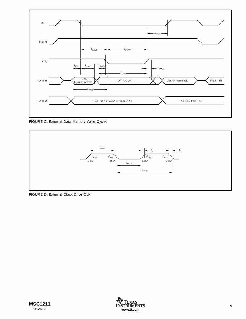
FIGURE C. External Data Memory Write Cycle.
FIGURE D. External Clock Drive CLK.
trtHIGH
VIH1 VIH1
0.8V 0.8V
VIH1 VIH1
0.8V 0.8VtLOW
tOSC
tf
MSC121110SBAS267www.ti.com
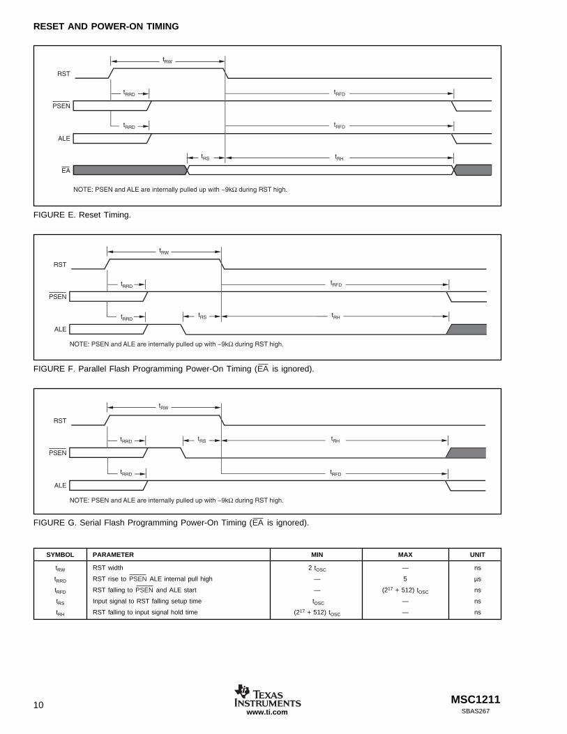
RESET AND POWER-ON TIMING
FIGURE E. Reset Timing.
FIGURE F. Parallel Flash Programming Power-On Timing (EA is ignored).
FIGURE G. Serial Flash Programming Power-On Timing (EA is ignored).
SYMBOL PARAMETER MIN MAX UNIT
tRW RST width 2 tOSC — ns
tRRD RST rise to PSEN ALE internal pull high — 5 µs
tRFD RST falling to PSEN and ALE start — (217 + 512) tOSC ns
tRS Input signal to RST falling setup time tOSC — ns
tRH RST falling to input signal hold time (217 + 512) tOSC — ns

MSC1211 11SBAS267 www.ti.com
48
47
46
45
44
43
42
41
40
39
38
37
36
35
34
33
EA
P0.6/AD6
P0.7/AD7
ALE
PSEN/OSCCLK/MODCLK
P2.7/A15
DVDD
DGND
P2.6/A14
P2.5/A13
P2.4/A12
P2.3/A11
P2.2/A10
P2.1/A09
P2.0/A08
NC
1
2
3
4
5
6
7
8
9
10
11
12
13
14
15
16
XOUT
XIN
P3.0/RxD0
P3.1/TxD0
P3.2/INT0
P3.3/INT1/TONE/PWM
P3.4/T0
P3.5/T1
P3.6/WR
P3.7/RD
DVDD
DGND
RST
DVDD
DVDD
RDAC0
P1.
7/IN
T5/
SC
LK/S
CK
P1.
6/IN
T4/
MIS
O/S
DA
P1.
5/IN
T3/
MO
SI
P1.
4/IN
T2/
SS
P1.
3/T
xD1
P1.
2/R
xD1
DV
DD
DG
ND
P1.
1/T
2EX
P1.
0/T
2
P0.
0/A
D0
P0.
1/A
D1
P0.
2/A
D2
P0.
3/A
D3
P0.
4/A
D4
P0.
5/A
D5
VD
AC
0
IDA
C0/
AIN
0
IDA
C1/
AIN
1
VD
AC
2/A
IN2
VD
AC
3/A
IN3
AIN
4
AIN
5
AIN
6/E
XT
D
AIN
7/E
XT
A
AIN
CO
M
AG
ND
AV
DD
RE
F IN
–
RE
FO
UT
/RE
F IN
+
VD
AC
1
RD
AC
1
64 63 62 61 60 59 58 57 56 55 54
17 18 19 20 21 22 23 24 25 26 27
53 52 51 50 49
28 29 30 31 32
MSC1211
PIN CONFIGURATION
PIN # NAME DESCRIPTION
1 XOUT The crystal oscillator pin XOUT supports parallel resonant AT cut crystals and ceramic resonators. XOUT serves as the outputof the crystal amplifier.
2 XIN The crystal oscillator pin XIN supports parallel resonant AT cut crystals and ceramic resonators. XIN can also be an input ifthere is an external clock source instead of a crystal.
3-10 P3.0-P3.7 Port 3 is a bidirectional I/O port. The alternate functions for Port 3 are listed below.Port 3—Alternate Functions:
PIN DESCRIPTIONS
Top View TQFP
11, 14, 15, 42, 58 DVDD Digital Power Supply12, 41, 57 DGND Digital Ground
13 RST A HIGH on the reset input for two tOSC periods will reset the device.16 RDAC0 RDAC0 Output17 VDAC0 VDAC0 Output27 AGND Analog Ground18 IDAC0/AIN0 IDAC0 Output/Analog Input Channel 0
19 IDAC1/AIN1 IDAC1 Output/Analog Input Channel 1
PORT ALTERNATE MODE
P3.0 RxD0 Serial Port 0 InputP3.1 TxD0 Serial Port 0 OutputP3.2 INT0 External Interrupt 0P3.3 INT1/TONE/PWM External Interrupt 1/TONE/PWM OutputP3.4 T0 Timer 0 External InputP3.5 T1 Timer 1 External InputP3.6 WR External Data Memory Write StrobeP3.7 RD External Data Memory Read Strobe

MSC121112SBAS267www.ti.com
PIN DESCRIPTIONS (Cont.)
20 VDAC2/AIN2 VDAC2 Output/Analog Input Channel 2
21 VDAC3/AIN3 VDAC3 Output/Analog Input Channel 3
22 AIN4 Analog Input Channel 4
23 AIN5 Analog Input Channel 5
24 AIN6, EXTD Analog Input Channel 6, Low Voltage Detect Input Generates DLVD Interrupt
25 AIN7, EXTA Analog Input Channel 7, Low Voltage Detect Input Generates ALVD Interrupt
26 AINCOM Analog Common for Single-Ended Inputs
28 AVDD Analog Power Supply29 REF IN– Voltage Reference Negative Input
30 REFOUT/REF IN+ Voltage Reference Output/ Voltage Reference Positive Input
31 VDAC1 VDAC1 Output
32 RDAC1 RDAC1 Output
33 NC No Connection
34-40, 43 P2.0-P2.7 Port 2 is a bidirectional I/O port. The alternate functions for Port 2 are listed below.Port 2—Alternate Functions:
PIN # NAME DESCRIPTION
ALE PSEN PROGRAM MODE SELECTION DURING RESET
NC NC Normal Operation (user application mode)0 NC Parallel Programming
NC 0 Serial Programming0 0 Reserved
PORT ALTERNATE MODE
P2.0 A8 Address Bit 8P2.1 A9 Address Bit 9P2.2 A10 Address Bit 10P2.3 A11 Address Bit 11P2.4 A12 Address Bit 12P2.5 A13 Address Bit 13P2.6 A14 Address Bit 14P2.7 A15 Address Bit 15
44 PSEN Program Store Enable: Connected to optional external memory as a chip enable. PSEN will provide an active low pulse.OSCCLK In programming mode, PSEN is used as an input along with ALE to define serial or parallel programming mode.MODCLK PSEN is held HIGH for parallel programming and tied LOW for serial programming. This pin can also be selected (when not
using external memory) to output the Oscillator clock, Modulator clock, HIGH, or LOW for light loads.
45 ALE Address Latch Enable: Used for latching the low byte of the address during an access to external memory. ALE is emittedat a constant rate of 1/2 the oscillator frequency, and can be used for external timing or clocking. One ALE pulse is skippedduring each access to external data memory. In programming mode, ALE is used as an input along with PSEN to defineserial or parallel programming mode. ALE is held HIGH for serial programming and tied LOW for parallel programming. Thispin can also be selected (when not using external memory) to output HIGH or LOW for light loads.
48 EA External Access Enable: EA must be externally held LOW to enable the device to fetch code from external program memorylocations starting with 0000H.
46, 47, 49-54 P0.0-P0.7 Port 0 is a bidirectional I/O port. The alternate functions for Port 0 are listed below.Port 0—Alternate Functions:
PORT ALTERNATE MODE
P0.0 AD0 Address/Data Bit 0P0.1 AD1 Address/Data Bit 1P0.2 AD2 Address/Data Bit 2P0.3 AD3 Address/Data Bit 3P0.4 AD4 Address/Data Bit 4P0.5 AD5 Address/Data Bit 5P0.6 AD6 Address/Data Bit 6P0.7 AD7 Address/Data Bit 7
55, 56, 59-64 P1.0-P1.7 Port 1 is a bidirectional I/O port. The alternate functions for Port 1 are listed below.Port 1—Alternate Functions: PORT ALTERNATE MODE
P1.0 T2 T2 InputP1.1 T2EX T2 External InputP1.2 RxD1 Serial Port InputP1.3 TxD1 Serial Port OutputP1.4 INT2/SS External Interrupt/Slave SelectP1.5 INT3/MOSI External Interrupt/Master Out-Slave InP1.6 INT4/MISO External Interrupt/Master In-Slave Out/SDAP1.7 INT5/SCK External Interrupt/Serial Clock/SCK

MSC1211 13SBAS267 www.ti.com
TYPICAL CHARACTERISTICSAVDD = +5V, DVDD = +5V, fOSC = 8MHz, PGA = 1, fMOD = 15.625kHz, Bipolar, Buffer On, and VREF ≡ (REF IN+) – (REF IN–) = +2.5V, unless otherwise specified.For VDAC, VREF = AVDD, RLOAD = 10kΩ, and CLOAD = 200pF, unless otherwise noted.
22
21
20
19
18
17
16
15
14
13
12
EFFECTIVE NUMBER OF BITSvs DECIMATION RATIO
Decimation Ratio =fMOD
fDATA
0 500 1000 1500 2000
PGA4
EN
OB
(rm
s)
PGA1 PGA2
PGA16
PGA8
PGA32 PGA64 PGA128
Sinc3 Filter, Buffer OFF
22
21
20
19
18
17
16
15
14
13
12
EFFECTIVE NUMBER OF BITSvs DECIMATION RATIO
0 500 1000 1500 2000
EN
OB
(rm
s)
PGA4 PGA8
PGA1
PGA2
PGA16
PGA32 PGA64 PGA128
Decimation Ratio =fMOD
fDATA
Sinc3 Filter, Buffer ON
22
21
20
19
18
17
16
15
14
13
12
EFFECTIVE NUMBER OF BITSvs DECIMATION RATIO
0 500 1000 1500 2000
EN
OB
(rm
s)
PGA4 PGA8PGA1 PGA2
PGA16PGA32
PGA64 PGA128
Decimation Ratio =fMOD
fDATA
AVDD = 3V, Sinc3 Filter,VREF = 1.25V, Buffer OFF
22
21
20
19
18
17
16
15
14
13
12
EFFECTIVE NUMBER OF BITSvs DECIMATION RATIO
0 500 1000 1500 2000
EN
OB
(rm
s)
PGA4 PGA8
PGA1
PGA2
PGA16 PGA32 PGA64 PGA128
AVDD = 3V, Sinc3 Filter,VREF = 1.25V, Buffer ON
Decimation Ratio =fMOD
fDATA
22
21
20
19
18
17
16
15
14
13
12
EFFECTIVE NUMBER OF BITSvs DECIMATION RATIO
0 500 1000 1500 2000
EN
OB
(rm
s)
PGA4 PGA8
PGA1
PGA2
PGA32 PGA128PGA16 PGA64
Decimation Ratio =fMOD
fDATA
Sinc2 Filter
EFFECTIVE NUMBER OF BITS vs DATA RATE2322212019181716151413121110
EN
OB
(rm
s)
Data Rate (SPS)1 10 100 1000
Sinc3 Filter, Buffer OFF
PGA1PGA8
PGA32PGA64
PGA128

MSC121114SBAS267www.ti.com
TYPICAL CHARACTERISTICS (Cont.)AVDD = +5V, DVDD = +5V, fOSC = 8MHz, PGA = 1, fMOD = 15.625kHz, Bipolar, Buffer On, and VREF ≡ (REF IN+) – (REF IN–) = +2.5V, unless otherwise specified.For VDAC, VREF = AVDD, RLOAD = 10kΩ, and CLOAD = 200pF, unless otherwise noted.
22
21
20
19
18
17
16
15
14
13
12
FAST SETTLING FILTEREFFECTIVE NUMBER OF BITS vs DECIMATION RATIO
0 500 1000 1500 2000
EN
OB
(rm
s)
1500
Decimation Ratio =fMOD
fDATA
Fast Settling Filter
EFFECTIVE NUMBER OF BITS vs fMOD(set with ACLK)
25
20
15
10
5
0
EN
OB
(rm
s)
Data Rate (SPS)1 10 100 1k 10k 100k
fMOD = 15.6kHz
fMOD = 62.5kHz
fMOD = 203kHz
fMOD = 110kHz
fMOD = 31.25kHz
EFFECTIVE NUMBER OF BITS vs fMOD (set with ACLK)WITH FIXED DECIMATION
25
20
15
10
5
0
EN
OB
(rm
s)
Data Rate (SPS)10 100 1k 10k 100k
DEC = 2020
DEC = 255
DEC = 500
DEC = 50
DEC = 20
DEC = 10
0.8
0.7
0.6
0.5
0.4
0.3
0.2
0.1
0
NOISE vs INPUT SIGNAL
VIN (V)
–2.5 –1.5 0.5–0.5 1.5 2.5
Noi
se (
rms,
ppm
of F
S)
10
8
6
4
2
0
–2
–4
–6
–8
–10
INTEGRAL NON-LINEARITY vs INPUT SIGNAL
VIN (V)
–2.5 –2 –1 –0.5–1.5 0 0.5 1 1.5 2 2.5
INL
(ppm
of F
S)
–40°C
+25°C
VREF = 2.5V
+85°C
30
20
10
0
–10
–20
–30
INTEGRAL NON-LINEARITY vs INPUT SIGNAL
VIN (V)
VIN = –VREF 0 VIN = +VREF
VREF = AVDD, Buffer OFF
INL
(ppm
of F
S)

MSC1211 15SBAS267 www.ti.com
TYPICAL CHARACTERISTICS (Cont.)AVDD = +5V, DVDD = +5V, fOSC = 8MHz, PGA = 1, fMOD = 15.625kHz, Bipolar, Buffer On, and VREF ≡ (REF IN+) – (REF IN–) = +2.5V, unless otherwise specified.For VDAC, VREF = AVDD, RLOAD = 10kΩ, and CLOAD = 200pF, unless otherwise noted.
900
800
700
600
500
400
300
200
100
0
ADC CURRENT vs PGA
PGA Setting
0 1 82 4 3216 12864
I AD
C (
µA)
AVDD = 5V, Buffer = ON
AVDD = 3V, Buffer = ON
Buffer = OFF
Buffer = OFF
4500
4000
3500
3000
2500
2000
1500
1000
500
0
HISTOGRAM OF OUTPUT DATA
ppm of FS
–2
Num
ber
of O
ccur
renc
es
–1.5 –1 –0.5 0 0.5 1 1.5 2
2.510
2.508
2.506
2.504
2.502
2.500
2.498
2.496
2.494
2.492
2.490
VREFOUT vs LOAD CURRENT
VREFOUT Current Load (mA)
0 0.4 0.8 1.2 1.6 2.0 2.4
VR
EF
OU
T (
V)
35
30
25
20
15
10
5
0
ADC INTEGRAL NONLINEARITY vs VREF
VREF (V)
0 0.5 1.0 1.5 2.0 2.5 3.0 3.5 4.0 4.5 5.0 5.5
AD
C IN
L (p
pm o
f FS
)
VIN = VREFBuffer OFF
AVDD = 3V
AVDD = 5V
INL ERROR vs PGA
PGA Setting
INL
(ppm
of F
S)
1 42 168 1286432
100
90
80
70
60
50
40
30
20
10
0
2.6
2.5
2.4
2.3
2.2
2.1
2.0
1.9
1.8
1.7
1.6
1.5
MAXIMUM ANALOG SUPPLY CURRENT
Analog Supply Voltage (V)
2.5 3.0 3.5 4.0 4.5 5.0 5.5
Ana
log
Sup
ply
Cur
rent
(m
A)
PGA = 128, ADC ON,Brownout Detect ON,All VDACs ON = FFFFH,VDACs REF = AVDD
–40°C
+25°C
+85°C

MSC121116SBAS267www.ti.com
TYPICAL CHARACTERISTICS (Cont.)AVDD = +5V, DVDD = +5V, fOSC = 8MHz, PGA = 1, fMOD = 15.625kHz, Bipolar, Buffer On, and VREF ≡ (REF IN+) – (REF IN–) = +2.5V, unless otherwise specified.For VDAC, VREF = AVDD, RLOAD = 10kΩ, and CLOAD = 200pF, unless otherwise noted.
NORMALIZED GAIN vs PGA
PGA Setting
Nor
mal
ized
Gai
n (%
)
1 42 168 1286432
101
100
99
98
97
96
DIGITAL SUPPLY CURRENT vs SUPPLY VOLTAGE
Supply Voltage (V)
Dig
ital S
uppl
y C
urre
nt (
mA
)
2.5 3.0 3.5 4.0 4.5 5.0 5.5
20
15
10
5
0
–40°C
+85°C
+25°C
DIGITAL SUPPLY CURRENT vs FREQUENCY
Clock Frequency (MHz)
Dig
ital S
uppl
y C
urre
nt (
mA
)
0.1 1 10 100
100
10
1
0.1
RUN
IDLE
DIGITAL SUPPLY CURRENT vs CLOCK DIVIDER
Clock Frequency (MHz)
Dig
ital S
uppl
y C
urre
nt (
mA
)
0.1 1 10 100
100
10
1
0.1
2
4
8
16
32
4096
1024
Divider Values
2048
10
8
6
4
2
0
–2
–4
–6
–8
–10
–12
OFFSET DAC: OFFSET vs TEMPERATURE
Offs
et (
ppm
of F
SR
)
Temperature (°C)
–40 +25 +85
1.00006
1.00004
1.00002
1
0.99998
0.99996
0.99994
OFFSET DAC: GAIN vs TEMPERATURE
Nor
mal
ized
Gai
n
Temperature (°C)
–40 +25 +85

MSC1211 17SBAS267 www.ti.com
CMOS DIGITAL OUTPUT
Output Current (mA)
Out
put V
olta
ge (
V)
0 2010 4030 706050
5.0
4.5
4.0
3.5
3.0
2.5
2.0
1.5
1.0
0.5
0
3VLow
Output
5VLow
Output
5V
3V
TYPICAL CHARACTERISTICS (Cont.)AVDD = +5V, DVDD = +5V, fOSC = 8MHz, PGA = 1, fMOD = 15.625kHz, Bipolar, Buffer On, and VREF ≡ (REF IN+) – (REF IN–) = +2.5V, unless otherwise specified.For VDAC, VREF = AVDD, RLOAD = 10kΩ, and CLOAD = 200pF, unless otherwise noted.
VDAC DIFFERENTIAL NONLINEARITY vs CODE
DN
L (L
SB
)
1.0
0.8
0.6
0.4
0.2
0
–0.2
–0.4
–0.6
–0.8
–1.0
0000H
DAC Code
2000H 4000H 6000H 8000H A000H C000H E000H FFFFH
VDAC INTEGRAL NONLINEARITY vs CODE
0000H
INL
(LS
B)
DAC Code
2000H 4000H 6000H 8000H A000H C000H E000H FFFFH
40
20
0
–20
–40
–40°C
+85°C
+25°C
5.0
4.9
4.8
4.7
4.6
4.5
VDAC SOURCE CURRENT CAPABILITY
VD
AC O
utpu
t (V
)
ISOURCE (mA)
0 4 6 1082 12 14 16
DAC = All 1s
0.6
0.5
0.4
0.3
0.2
0.1
0
VDAC SINK CURRENT CAPABILITY
VD
AC O
utpu
t (V
)
ISINK (mA)
0 4 6 1082 12 14 16
DAC = All 0s
VDAC FULL-SCALE ERROR vs LOAD RESISTOR
0.5
Err
or (%
of F
S)
Load Resistor (kΩ)
1 10 100 1k 10k
1
0
–1
–2
–3
–4
–5
MSC121118SBAS267www.ti.com
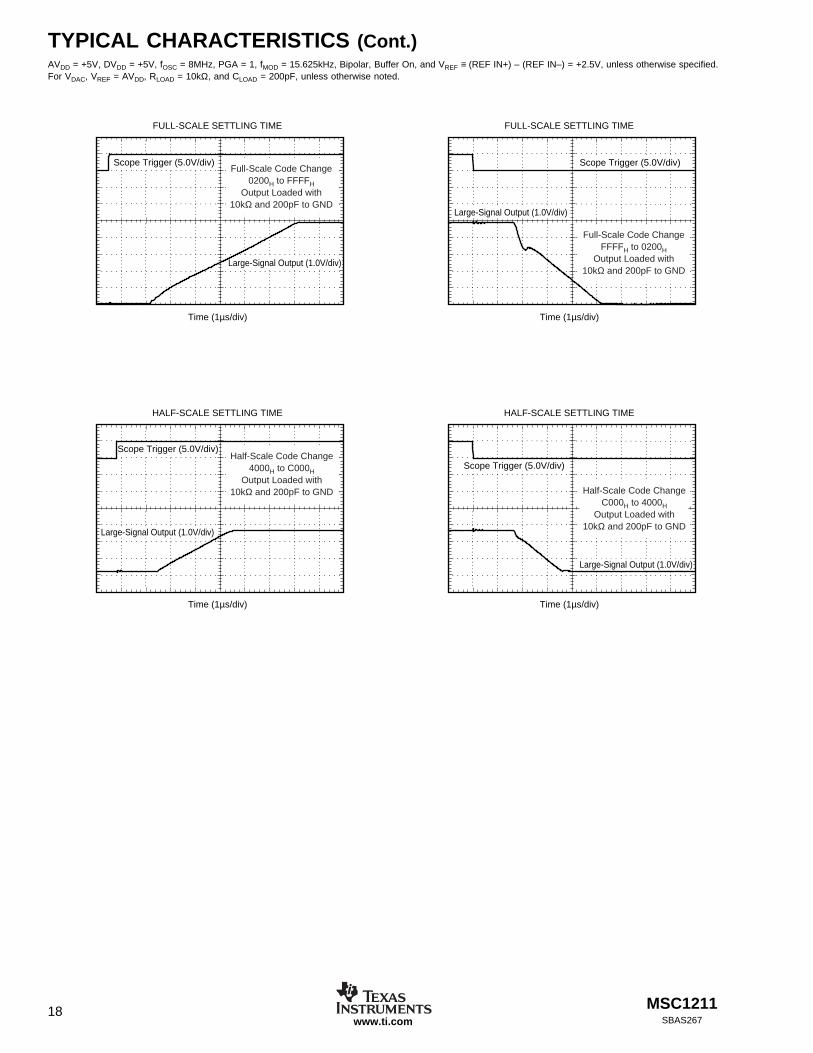
TYPICAL CHARACTERISTICS (Cont.)AVDD = +5V, DVDD = +5V, fOSC = 8MHz, PGA = 1, fMOD = 15.625kHz, Bipolar, Buffer On, and VREF ≡ (REF IN+) – (REF IN–) = +2.5V, unless otherwise specified.For VDAC, VREF = AVDD, RLOAD = 10kΩ, and CLOAD = 200pF, unless otherwise noted.
HALF-SCALE SETTLING TIME
Time (1µs/div)
Scope Trigger (5.0V/div)
Large-Signal Output (1.0V/div)
Half-Scale Code ChangeC000H to 4000H
Output Loaded with10kΩ and 200pF to GND
HALF-SCALE SETTLING TIME
Time (1µs/div)
Scope Trigger (5.0V/div)
Large-Signal Output (1.0V/div)
Half-Scale Code Change4000H to C000H
Output Loaded with10kΩ and 200pF to GND
FULL-SCALE SETTLING TIME
Time (1µs/div)
Scope Trigger (5.0V/div)
Large-Signal Output (1.0V/div)
Full-Scale Code ChangeFFFFH to 0200H
Output Loaded with10kΩ and 200pF to GND
FULL-SCALE SETTLING TIME
Time (1µs/div)
Scope Trigger (5.0V/div)
Large-Signal Output (1.0V/div)
Full-Scale Code Change0200H to FFFFH
Output Loaded with10kΩ and 200pF to GND

MSC1211 19SBAS267 www.ti.com
The MSC1211Yx allows the user to uniquely configure theFlash and SRAM memory maps to meet the needs of theirapplication. The Flash is programmable down to 2.7V usingboth serial and parallel programming methods. The Flashendurance is 100k Erase/Write cycles. In addition, 1280bytes of RAM are incorporated on-chip.
The part has separate analog and digital supplies, which canbe independently powered from 2.7V to +5.5V. At +3V opera-tion, the power dissipation for the part is typically less than4mW. The MSC1211Yx is packaged in a TQFP-64 package.
The MSC1211Yx is designed for high-resolution measurementapplications in smart transmitters, industrial process control,weigh scales, chromatography, and portable instrumentation.
ENHANCED 8051 CORE
All instructions in the MSC1211 family perform exactly the samefunctions as they would in a standard 8051. The effect on bits,flags, and registers is the same. However, the timing is different.The MSC1211 family utilizes an efficient 8051 core which resultsin an improved instruction execution speed of between 1.5 and3 times faster than the original core for the same external clockspeed (4 clock cycles per instruction versus 12 clock cycles perinstruction, as shown in Figure 2). This translates into an effectivethroughput improvement of more than 2.5 times, using the samecode and same external clock speed. Therefore, a devicefrequency of 30MHz for the MSC1211Yx actually performs at an
DESCRIPTIONThe MSC1211Yx is a completely integrated family of mixed-signal devices incorporating a high-resolution delta-sigmaADC, quad 16-bit DACs, 8-channel multiplexer, burnoutdetect current sources, selectable buffered input, offset DAC(Digital-to-Analog Converter), Programmable Gain Amplifier(PGA), temperature sensor, voltage reference, 8-bit micro-controller, Flash Program Memory, Flash Data Memory, andData SRAM, as shown in Figure 1.
On-chip peripherals include an additional 32-bit accumulator, anSPI compatible serial port with FIFO, I2C, dual UARTs, multipledigital input/output ports, watchdog timer, low-voltage detect,on-chip power-on reset, 16-bit PWM, breakpoints, brownoutreset, three timer/counters, and a system clock divider.
The device accepts low-level differential or single-endedsignals directly from a transducer. The ADC provides 24 bitsof resolution and 24 bits of no-missing-code performanceusing a sinc3 filter with a programmable sample rate. TheADC also has a selectable filter that allows for high-resolu-tion single-cycle conversion.
The microcontroller core is 8051 instruction set compatible. Themicrocontroller core is an optimized 8051 core which executes upto three times faster than the standard 8051 core, given the sameclock source. That makes it possible to run the device at a lowerexternal clock frequency and achieve the same performance atlower power than the standard 8051 core.
ACC
MUX
AGND
+AVDD
AVDD
BUF PGA
VREF
Modulator
Up to 32KFLASH
1.2KSRAM
SPIFIFO
DigitalFilter
8051
SFR
SYS ClockDivider
LVD
BOR
POR
PORT1
PORT2
WDT
Timers/Counters
ClockGenerator
PORT0
PORT3
8
8
8
EA
8
T2SPI/EXT/I2CUART2
ADDR
ADDRDATA
AlternateFunctions
UART1EXTT0T1PWMRW
8-BitOffset DACIDAC0/AIN0
IDAC1/AIN1
VDAC2/AIN2
VDAC3/AIN3
AIN4
AIN5
AIN6
AIN7
AINCOM
AGND REFOUT/REF IN+ REF IN– DVDD DGND
XIN XOUT
VDAC0
VDAC1
VDAC2
VDAC3
AIN2
AIN3
VDAC1VDAC0
ALE
PSEN
V/IConverter
V/IConverter
TemperatureSensor
RST
RDAC1
IDAC0/AIN0
IDAC1/AIN1
RDAC0
FIGURE 1. Block Diagram.
FIGURE 2. Instruction Cycle Timing.
CLK
instr_cycle
cpu_cycle C1 C2 C3 C4 C1 C2 C3 C4 C1
n + 1 n + 2

MSC121120SBAS267www.ti.com
equivalent execution speed of 75MHz compared to the standard8051 core. This allows the user to run the device at slowerexternal clock speeds which reduces system noise and powerconsumption, but provides greater throughput. This performancedifference can be seen in Figure 3. The timing of software loopswill be faster with the MSC1211. However, the timer/counteroperation of the MSC1211 may be maintained at 12 clocks perincrement or optionally run at 4 clocks per increment.
Furthermore, improvements were made to peripheral featuresthat offload processing from the core, and the user, to furtherimprove efficiency. For instance, the SPI interface uses a FIFO,which allows the SPI interface to transmit and receive data withminimum overhead needed from the core. Also, a 32-bit accu-mulator was added to significantly reduce the processing over-head for the multiple byte data from the ADC or other sources.This allows for 24-bit addition and shifting to be accomplishedin a few instruction cycles, compared to hundreds of instructioncycles through software implementation.
Family Device Compatibility
The hardware functionality and pin configuration across theMSC1211 family is fully compatible. To the user the only differ-ence between family members is the memory configuration. Thismakes migration between family members simple. Code writtenfor the MSC1211Y2 can be executed directly on an MSC1211Y3,MSC1211Y4, or MSC1211Y5. This gives the user the ability toadd or subtract software functions and to freely migrate betweenfamily members. Thus, the MSC1211 can become a standarddevice used across several application platforms.
Family Development Tools
The MSC1211 is fully compatible with the standard 8051instruction set. This means that the user can develop soft-ware for the MSC1211 with their existing 8051 developmenttools. Additionally, a complete, integrated development envi-ronment is provided with each demo board, and third-partydevelopers also provide support.
Power Down Modes
The MSC1211 can power several of the peripherals and putthe CPU into IDLE. This is accomplished by shutting off theclocks to those sections, as shown in Figure 4.
FIGURE 3. Comparison of MSC1211 Timing to Standard8051 Timing.
USECFB
MSECH
HMSECFE
MSINTFA
ACLKF6
divideby 64
MSECLFD FC
ms
µs
100ms
Flash WriteTiming
Flash EraseTiming
WDTCON
SECINTF9
FF
FTCON[3:0]
FTCON[7:4]
EF
EF
secondsinterrupt
watchdog
millisecondsinterrupt
ADC Output RateADCON3 ADCON2DF DE
Decimation Ratio
SYS ClockOscillator
PWMHI PWMLOWA3 A2
PWM Clock
SPICON/I2CCON 9A
SCLK/SCK
tCLK
tOSC
(30µs to 40µs)
(5ms to 11ms)
STOP
PDCON.0
PDCON.4
PDCON.1
Modulator Clock
PDCON.2
PDCON.3
IDLECPU Clock
Timers 0/1/2
SYS ClockDivider
ADC Power Down
UART0/1
CKCON INSTRUCTION RD or WR RD or WR(8EH) CYCLES STROBE WIDTH STROBE WIDTH
MD2:MD0 (for MOVX) (SYS CLKs) (µs) AT 12MHz
000 2 2 0.167001 3 (default) 4 0.333010 4 8 0.667011 5 12 1.000100 6 16 1.333101 7 20 1.667110 8 24 2.000111 9 28 2.333
TABLE I. Memory Cycle Stretching. Stretching of MOVXtiming as defined by MD2, MD1, and MD0 bits inCKCON register (address 8EH).
The MSC1211 also provides dual data pointers (DPTRs) tospeed block Data Memory moves.
Additionally, it can stretch the number of memory cycles toaccess external Data Memory from between two and nineinstruction cycles in order to accommodate different speeds ofmemory or devices, as shown in Table I. The MSC1211provides an external memory interface with a 16-bit addressbus (P0 and P2). The 16-bit address bus makes it necessaryto multiplex the low address byte through the P0 port. Toenhance P0 and P2 for high-speed memory access, hardwareconfiguration control is provided to configure the ports forexternal memory/peripheral interface or general-purpose I/O.
FIGURE 4. MSC1211 Timing Chain and Clock Control.
ALE
PSEN
AD0-AD7
PORT 2
ALE
PSEN
AD0-AD7
PORT 2
CLK
Sta
nd
ard
805
1 Ti
min
gM
SC
1210
Tim
ing
Single-Byte, Single-CycleInstruction
Single-Byte, Single-CycleInstruction
12 Cycles
4 Cycles

MSC1211 21SBAS267 www.ti.com
OVERVIEWINPUT MULTIPLEXER
The input multiplexer provides for any combination of differentialinputs to be selected as the input channel, as shown in Figure 5.If AIN0 is selected as the positive differential input channel, anyother channel can be selected as the negative differential inputchannel. With this method, it is possible to have up to eight fullydifferential input channels. It is also possible to switch the polarityof the differential input pair to negate any offset voltages.
FIGURE 5. Input Multiplexer Configuration. FIGURE 6. Analog Input Structure.
In addition, current sources are supplied that will source orsink current to detect open or short circuits on the pins.
TEMPERATURE SENSOR
On-chip diodes provide temperature sensing capability. Whenthe configuration register for the input MUX is set to all 1s,the diodes are connected to the input of the ADC. All otherchannels are open.
BURNOUT DETECT
When the Burnout Detect (BOD) bit is set in the ADC controlconfiguration register (ADCON0 DCH), two current sources areenabled. The current source on the positive input channel sourcesapproximately 2µA of current. The current source on the negativeinput channel sinks approximately 2µA. This allows for thedetection of an open circuit (full-scale reading) or short circuit(small differential reading) on the selected input differential pair.
INPUT BUFFERThe analog input impedance is always high, regardless ofPGA setting (when the buffer is enabled). With the bufferenabled, the input voltage range is reduced and the analogpower-supply current is higher. If the limitation of inputvoltage range is acceptable, then the buffer is always pre-ferred.
The input impedance of the MSC1211 without the bufferis 5MΩ/PGA. The buffer is controlled by the state of the BUFbit in the ADC control register (ADCON0 DCH).
ANALOG INPUT
When the buffer is not selected, the input impedance of theanalog input changes with ACLK clock frequency (ACLKF6H) and gain (PGA). The relationship is:
A pedanceMHz
ACLK FrequencyM
PGAIN Im ( )Ω =
• Ω
1 5
where ACLK frequency = fCLK/(ACLK +1).
Figure 6 shows the basic input structure of the MSC1211.The sampling frequency varies according to the PGA set-tings, as shown in Table II.
RSW(8kΩ typical)
Sampling Frequency = fSAMP
HighImpedance
> 1GΩCINT12pF Typical
VCM
AIN
AIN3
AIN4
AIN5
AIN6
AIN0
AIN1
AIN2
AIN7
AINCOM
Burnout DetectCurrent Source
Burnout DetectCurrent Sink
AGND
Temperature Sensor
I80 • I
AVDD
In+
In–
PGA FULL-SCALE RANGE SAMPLING FREQUENCY
1 ±VREF fSAMP
2 ±VREF/2 fSAMP
4 ±VREF/4 fSAMP
8 ±VREF/8 fSAMP • 216 ±VREF/16 fSAMP • 432 ±VREF/32 fSAMP • 864 ±VREF/64 fSAMP • 16128 ±VREF/128 fSAMP • 16
NOTE: fSAMP = ACLK frequency/64.
TABLE II. Sampling Frequency Versus PGA Setting.

MSC121122SBAS267www.ti.com
PGAThe PGA can be set to gains of 1, 2, 4, 8, 16, 32, 64, or 128.Using the PGA can actually improve the effective resolutionof the ADC. For instance, with a PGA of 1 on a ±2.5V full-scale range, the ADC can resolve to 1.5µV. With a PGA of128 on a ±19mV full-scale range, the ADC can resolve to75nV. With a PGA of 1 on a ±2.5V full-scale range, it wouldrequire a 26-bit ADC to resolve 75nV, as shown in Table III.
requires a positive “full-scale” differential input signal. It thencomputes a value to nullify gain errors in the system. Each ofthese calibrations will take seven tDATA periods to complete.
Calibration should be performed after power on, a change intemperature, decimation ratio, buffer, or a change of thePGA. Calibration will remove the effects of the Offset DAC,therefore, changes to the Offset DAC register must be doneafter calibration.
At the completion of calibration, the ADC Interrupt bit goesHIGH which indicates the calibration is finished and validdata is available.
DIGITAL FILTER
The Digital Filter can use either the Fast Settling, sinc2, orsinc3 filter, as shown in Figure 7. In addition, the Auto modechanges the sinc filter after the input channel or PGA ischanged. When switching to a new channel, it will use theFast Settling filter, for the next two conversions the first ofwhich should be discarded. It will then use the sinc2 followedby the sinc3 filter to improve noise performance. This com-bines the low-noise advantage of the sinc3 filter with thequick response of the Fast Settling Time filter. The frequencyresponse of each filter is shown in Figure 8.
FIGURE 7. Filter Step Responses.
SETTLING TIMEFILTER (Conversion Cycles)
Sinc3 3(1)
Sinc2 2(1)
Fast 1(1)
NOTE: (1) With Synchronized Channel Changes.
CONVERSION CYCLE
1 2 3 4+
Discard Fast Sinc2 Sinc3
AUTO MODE FILTER SELECTION
FILTER SETTLING TIME
Adjustable Digital Filter
Data OutModulator
Fast Settling
Sinc2
Sinc3
RMSFULL-SCALE MEASUREMENT EQUIVALENT
PGA RANGE ENOB RESOLUTION ENOB AT PGA = 1SETTING (V) AT 10Hz (nV) (5V RANGE)
1 ±2.5V 21.7 1468 21.72 ±1.25 21.5 843 22.54 ±0.625 21.4 452 23.48 ±0.313 21.2 259 24.216 ±0.156 20.8 171 24.832 ±0.0781 20.4 113 25.464 ±0.039 20 74.5 26128 ±0.019 19 74.5 26
TABLE III. ENOB Versus PGA.
OFFSET DACThe analog input to the PGA can be offset by up to half thefull-scale input range of the PGA by using the ODAC register(SFR E6H). The ODAC (Offset DAC) register is an 8-bitvalue; the MSB is the sign and the seven LSBs provide themagnitude of the offset. Since the ODAC introduces ananalog (instead of digital) offset to the PGA, using the ODACdoes not reduce the performance of the ADC.
MODULATOR
The modulator is a single-loop 2nd-order system. The modu-lator runs at a clock speed (fMOD) that is derived from the CLKusing the value in the Analog Clock register (ACLK). Thedata output rate is:
Data Rate = fMOD/Decimation Ratio
where fMOD = fCLK/(ACLK +1)/64
CALIBRATION
The offset and gain errors in the MSC1211, or the completesystem, can be reduced with calibration. Calibration is con-trolled through the ADCON1 register (SFR DDH), bitsCAL2:CAL0. Each calibration process takes seven tDATA
periods (data conversion time) to complete. Therefore, ittakes 14 tDATA periods to complete both an offset and gaincalibration.
For system calibration, the appropriate signal must beapplied to the inputs. The system offset command requires a“zero” differential input signal. It then computes an offset thatwill nullify offset in the system. The system gain command

MSC1211 23SBAS267 www.ti.com
VOLTAGE REFERENCE
The voltage reference used for the MSC1211 can either beinternal or external. The power-up configuration for the volt-age reference is 2.5V internal. The selection for the voltagereference is made through the ADCON0 register (SFR DCH).
The internal voltage reference is selectable as either 1.25V(AVDD = 2.7V to 5.25V) or 2.5V (AVDD = 4.5V to 5.25V). If theinternal VREF is not used, it should be turned off to reducenoise and power consumption. The VREFOUT pin should havea 0.1µF capacitor to AGND.
The external voltage reference is differential and is representedby the voltage difference between the pins: REF IN+ and REFIN–. The absolute voltage on either pin (REF IN+ and REF IN–) can range from AGND to AVDD, however, the differentialvoltage must not exceed 2.6V. The differential voltage referenceprovides easy means of performing ratiometric measurement.
DAC
The architecture consists of a string DAC followed by anoutput buffer amplifier. Figure 9 shows a block diagram of theDAC architecture.
FIGURE 8. Filter Frequency Responses.
SINC3 FILTER RESPONSE(–3dB = 0.262 • fDATA)
Frequency (Hz)
0
–20
–40
–60
–80
–100
–1200 fD 2fD 3fD 4fD 5fD
0 fD 2fD 3fD 4fD 5fD
0 fD 2fD 3fD 4fD 5fD
Gai
n (d
B)
SINC2 FILTER RESPONSE(–3dB = 0.318 • fDATA)
Frequency (Hz)
0
–20
–40
–60
–80
–100
–120
Gai
n (d
B)
FAST SETTLING FILTER RESPONSE(–3dB = 0.469 • fDATA)
Frequency (Hz)
0
–20
–40
–60
–80
–100
–120
NOTE: fD = Data Output Rate = 1/tDATA
Gai
n (d
B)
FIGURE 9. DAC Architecture.
DAC3
DAC2
DAC1
DAC0
21 AIN3/VDAC3
AIN2/VDAC2
VDAC1
VDAC0VREF
AVDD
AIN0/IDAC0
RDAC0
AIN1/IDAC1
RDAC1
20
31
19
32
17
V/I Converter
CurrentMirror
CurrentMirror
18
16
V/I Converter
The input coding to the DAC is straight binary, so the idealoutput voltage is given by:
VDAC VD
REF= •65536
where D = decimal equivalent of the binary code that isloaded to the DAC register; it can range from 0 to 65535.
MSC121124SBAS267www.ti.com
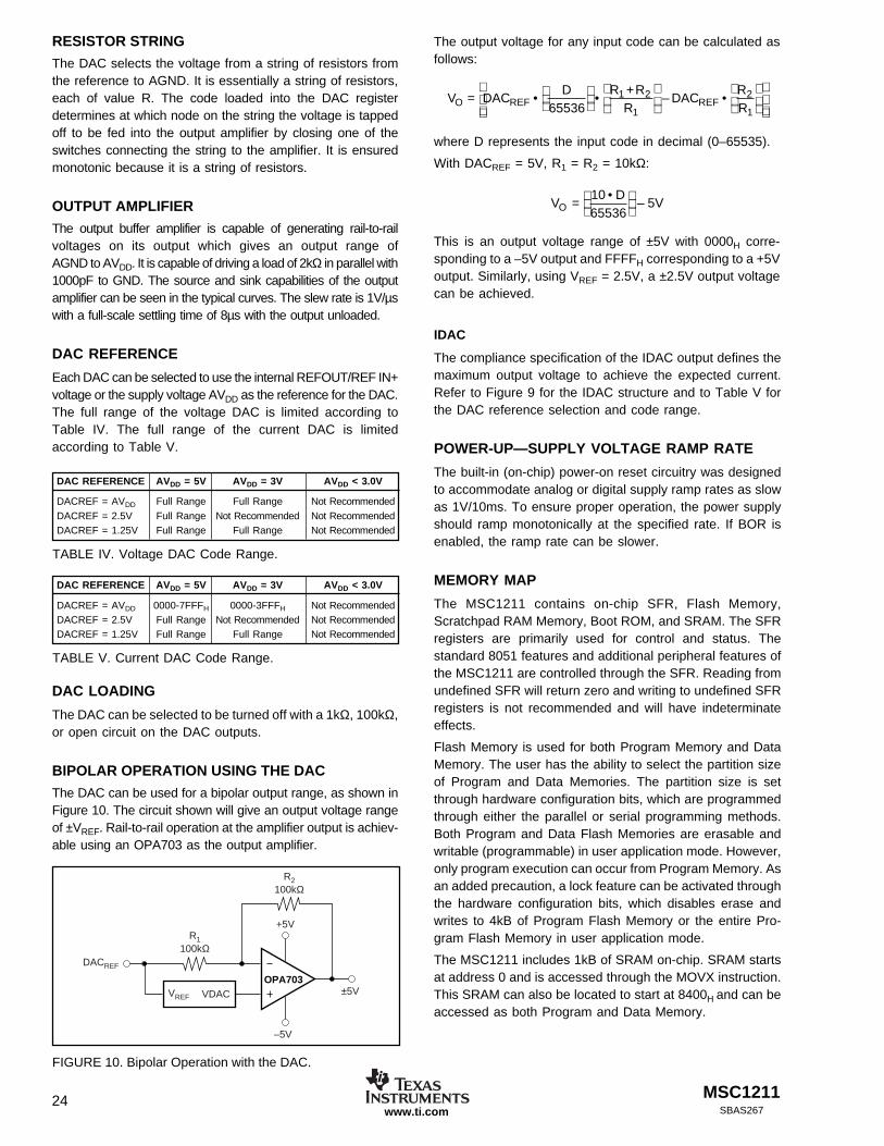
RESISTOR STRING
The DAC selects the voltage from a string of resistors fromthe reference to AGND. It is essentially a string of resistors,each of value R. The code loaded into the DAC registerdetermines at which node on the string the voltage is tappedoff to be fed into the output amplifier by closing one of theswitches connecting the string to the amplifier. It is ensuredmonotonic because it is a string of resistors.
OUTPUT AMPLIFIER
The output buffer amplifier is capable of generating rail-to-railvoltages on its output which gives an output range ofAGND to AVDD. It is capable of driving a load of 2kΩ in parallel with1000pF to GND. The source and sink capabilities of the outputamplifier can be seen in the typical curves. The slew rate is 1V/µswith a full-scale settling time of 8µs with the output unloaded.
DAC REFERENCE
Each DAC can be selected to use the internal REFOUT/REF IN+voltage or the supply voltage AVDD as the reference for the DAC.The full range of the voltage DAC is limited according toTable IV. The full range of the current DAC is limitedaccording to Table V.
The output voltage for any input code can be calculated asfollows:
V DACD R R
RDAC
RRO REF REF= •
• +
•
65536
1 2
1
2
1–
where D represents the input code in decimal (0–65535).
With DACREF = 5V, R1 = R2 = 10kΩ:
VD
VO = •
1065536
5–
This is an output voltage range of ±5V with 0000H corre-sponding to a –5V output and FFFFH corresponding to a +5Voutput. Similarly, using VREF = 2.5V, a ±2.5V output voltagecan be achieved.
IDAC
The compliance specification of the IDAC output defines themaximum output voltage to achieve the expected current.Refer to Figure 9 for the IDAC structure and to Table V forthe DAC reference selection and code range.
POWER-UP—SUPPLY VOLTAGE RAMP RATE
The built-in (on-chip) power-on reset circuitry was designedto accommodate analog or digital supply ramp rates as slowas 1V/10ms. To ensure proper operation, the power supplyshould ramp monotonically at the specified rate. If BOR isenabled, the ramp rate can be slower.
MEMORY MAP
The MSC1211 contains on-chip SFR, Flash Memory,Scratchpad RAM Memory, Boot ROM, and SRAM. The SFRregisters are primarily used for control and status. Thestandard 8051 features and additional peripheral features ofthe MSC1211 are controlled through the SFR. Reading fromundefined SFR will return zero and writing to undefined SFRregisters is not recommended and will have indeterminateeffects.
Flash Memory is used for both Program Memory and DataMemory. The user has the ability to select the partition sizeof Program and Data Memories. The partition size is setthrough hardware configuration bits, which are programmedthrough either the parallel or serial programming methods.Both Program and Data Flash Memories are erasable andwritable (programmable) in user application mode. However,only program execution can occur from Program Memory. Asan added precaution, a lock feature can be activated throughthe hardware configuration bits, which disables erase andwrites to 4kB of Program Flash Memory or the entire Pro-gram Flash Memory in user application mode.
The MSC1211 includes 1kB of SRAM on-chip. SRAM startsat address 0 and is accessed through the MOVX instruction.This SRAM can also be located to start at 8400H and can beaccessed as both Program and Data Memory.
FIGURE 10. Bipolar Operation with the DAC.
VREF VDAC
DACREF
R1100kΩ
R2100kΩ
–5V
±5V
+5V
OPA703
DAC REFERENCE AVDD = 5V AVDD = 3V AVDD < 3.0V
DACREF = AVDD Full Range Full Range Not RecommendedDACREF = 2.5V Full Range Not Recommended Not RecommendedDACREF = 1.25V Full Range Full Range Not Recommended
TABLE IV. Voltage DAC Code Range.
DAC REFERENCE AVDD = 5V AVDD = 3V AVDD < 3.0V
DACREF = AVDD 0000-7FFFH 0000-3FFFH Not RecommendedDACREF = 2.5V Full Range Not Recommended Not RecommendedDACREF = 1.25V Full Range Full Range Not Recommended
TABLE V. Current DAC Code Range.
DAC LOADING
The DAC can be selected to be turned off with a 1kΩ, 100kΩ,or open circuit on the DAC outputs.
BIPOLAR OPERATION USING THE DAC
The DAC can be used for a bipolar output range, as shown inFigure 10. The circuit shown will give an output voltage rangeof ±VREF. Rail-to-rail operation at the amplifier output is achiev-able using an OPA703 as the output amplifier.
MSC1211 25SBAS267 www.ti.com
HCR0 MSC1211Y2 MSC1211Y3 MSC1211Y4 MSC1211Y5
DFSEL PM DM PM DM PM DM PM DM
000 0000 0400- 0000 0400- 0000 0400- 0000 0400-13FF 23FF 43FF 83FF
001 0000 0400- 0000 0400- 0000 0400- 0000 0400-13FF 23FF 43FF 83FF
010 0000 0400 0000 0400 0000 0400 0000- 0400-13FF 23FF 43FF 3FFF 43FF
011 0000 0400- 0000 0400- 0000- 0400- 0000- 0400-13FF 23FF 1FFF 23FF 5FFF 23FF
100 0000 0400- 0000- 0400- 0000- 0400- 0000- 0400-13FF 0FFF 13FF 2FFF 13FF 6FFF 13FF
101 0000- 0400- 0000- 0400- 0000- 0400- 0000- 0400-07FF 0BFF 17FF 0BFF 37FF 0BFF 77FF 0BFF
110 0000- 0400- 0000- 0400- 0000- 0400- 0000- 0400-0BFF 07FF 1BFF 07FF 3BFF 07FF 7BFF 07FF
111 (default) 0000- 0000 0000- 0000 0000- 0000 0000- 00000FFF 1FFF 3FFF 7FFF
NOTE: Program memory accesses above the highest listed address willaccess external program memory.
TABLE VII. Flash Memory Partitioning.
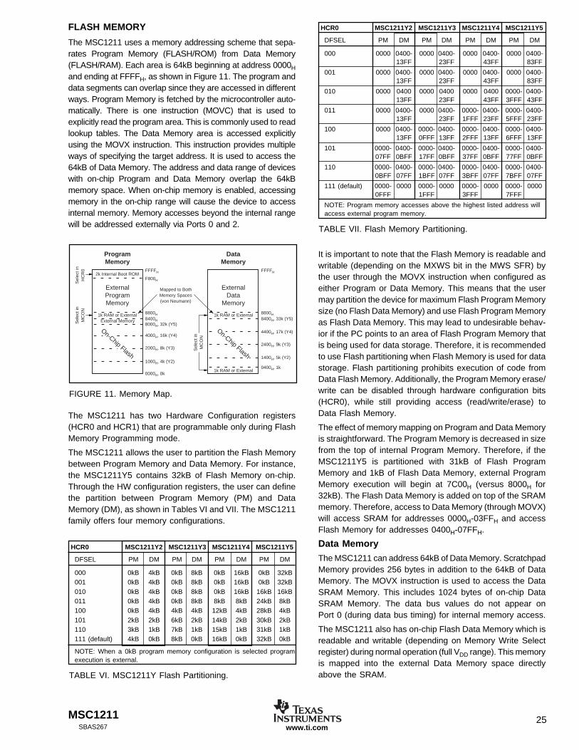
FLASH MEMORY
The MSC1211 uses a memory addressing scheme that sepa-rates Program Memory (FLASH/ROM) from Data Memory(FLASH/RAM). Each area is 64kB beginning at address 0000H
and ending at FFFFH, as shown in Figure 11. The program anddata segments can overlap since they are accessed in differentways. Program Memory is fetched by the microcontroller auto-matically. There is one instruction (MOVC) that is used toexplicitly read the program area. This is commonly used to readlookup tables. The Data Memory area is accessed explicitlyusing the MOVX instruction. This instruction provides multipleways of specifying the target address. It is used to access the64kB of Data Memory. The address and data range of deviceswith on-chip Program and Data Memory overlap the 64kBmemory space. When on-chip memory is enabled, accessingmemory in the on-chip range will cause the device to accessinternal memory. Memory accesses beyond the internal rangewill be addressed externally via Ports 0 and 2.
It is important to note that the Flash Memory is readable andwritable (depending on the MXWS bit in the MWS SFR) bythe user through the MOVX instruction when configured aseither Program or Data Memory. This means that the usermay partition the device for maximum Flash Program Memorysize (no Flash Data Memory) and use Flash Program Memoryas Flash Data Memory. This may lead to undesirable behav-ior if the PC points to an area of Flash Program Memory thatis being used for data storage. Therefore, it is recommendedto use Flash partitioning when Flash Memory is used for datastorage. Flash partitioning prohibits execution of code fromData Flash Memory. Additionally, the Program Memory erase/write can be disabled through hardware configuration bits(HCR0), while still providing access (read/write/erase) toData Flash Memory.
The effect of memory mapping on Program and Data Memoryis straightforward. The Program Memory is decreased in sizefrom the top of internal Program Memory. Therefore, if theMSC1211Y5 is partitioned with 31kB of Flash ProgramMemory and 1kB of Flash Data Memory, external ProgramMemory execution will begin at 7C00H (versus 8000H for32kB). The Flash Data Memory is added on top of the SRAMmemory. Therefore, access to Data Memory (through MOVX)will access SRAM for addresses 0000H-03FFH and accessFlash Memory for addresses 0400H-07FFH.
Data Memory
The MSC1211 can address 64kB of Data Memory. ScratchpadMemory provides 256 bytes in addition to the 64kB of DataMemory. The MOVX instruction is used to access the DataSRAM Memory. This includes 1024 bytes of on-chip DataSRAM Memory. The data bus values do not appear onPort 0 (during data bus timing) for internal memory access.
The MSC1211 also has on-chip Flash Data Memory which isreadable and writable (depending on Memory Write Selectregister) during normal operation (full VDD range). This memoryis mapped into the external Data Memory space directlyabove the SRAM.
HCR0 MSC1211Y2 MSC1211Y3 MSC1211Y4 MSC1211Y5
DFSEL PM DM PM DM PM DM PM DM
000 0kB 4kB 0kB 8kB 0kB 16kB 0kB 32kB001 0kB 4kB 0kB 8kB 0kB 16kB 0kB 32kB010 0kB 4kB 0kB 8kB 0kB 16kB 16kB 16kB011 0kB 4kB 0kB 8kB 8kB 8kB 24kB 8kB100 0kB 4kB 4kB 4kB 12kB 4kB 28kB 4kB101 2kB 2kB 6kB 2kB 14kB 2kB 30kB 2kB110 3kB 1kB 7kB 1kB 15kB 1kB 31kB 1kB111 (default) 4kB 0kB 8kB 0kB 16kB 0kB 32kB 0kB
NOTE: When a 0kB program memory configuration is selected programexecution is external.
TABLE VI. MSC1211Y Flash Partitioning.
FIGURE 11. Memory Map.
1k RAM or External1k RAM or External
1k RAM or External
External MemorySel
ect i
nM
CO
NS
elec
t in
HC
R0
0000H, 0k
2000H, 8k (Y3)
1000H, 4k (Y2)
4000H, 16k (Y4)
8400H8000H, 32k (Y5)
2k Internal Boot ROM F800H
FFFFH
ExternalProgramMemory
Mapped to BothMemory Spaces(von Neumann)
8800H
On-Chip Flash
Sel
ect i
nM
CO
N
0400H, 1k
1400H, 5k (Y2)
2400H, 9k (Y3)
4400H, 17k (Y4)
8400H, 33k (Y5)
FFFFH
ExternalData
Memory
ProgramMemory
DataMemory
8800H
On-Chip Flash
The MSC1211 has two Hardware Configuration registers(HCR0 and HCR1) that are programmable only during FlashMemory Programming mode.
The MSC1211 allows the user to partition the Flash Memorybetween Program Memory and Data Memory. For instance,the MSC1211Y5 contains 32kB of Flash Memory on-chip.Through the HW configuration registers, the user can definethe partition between Program Memory (PM) and DataMemory (DM), as shown in Tables VI and VII. The MSC1211family offers four memory configurations.
MSC121126SBAS267www.ti.com
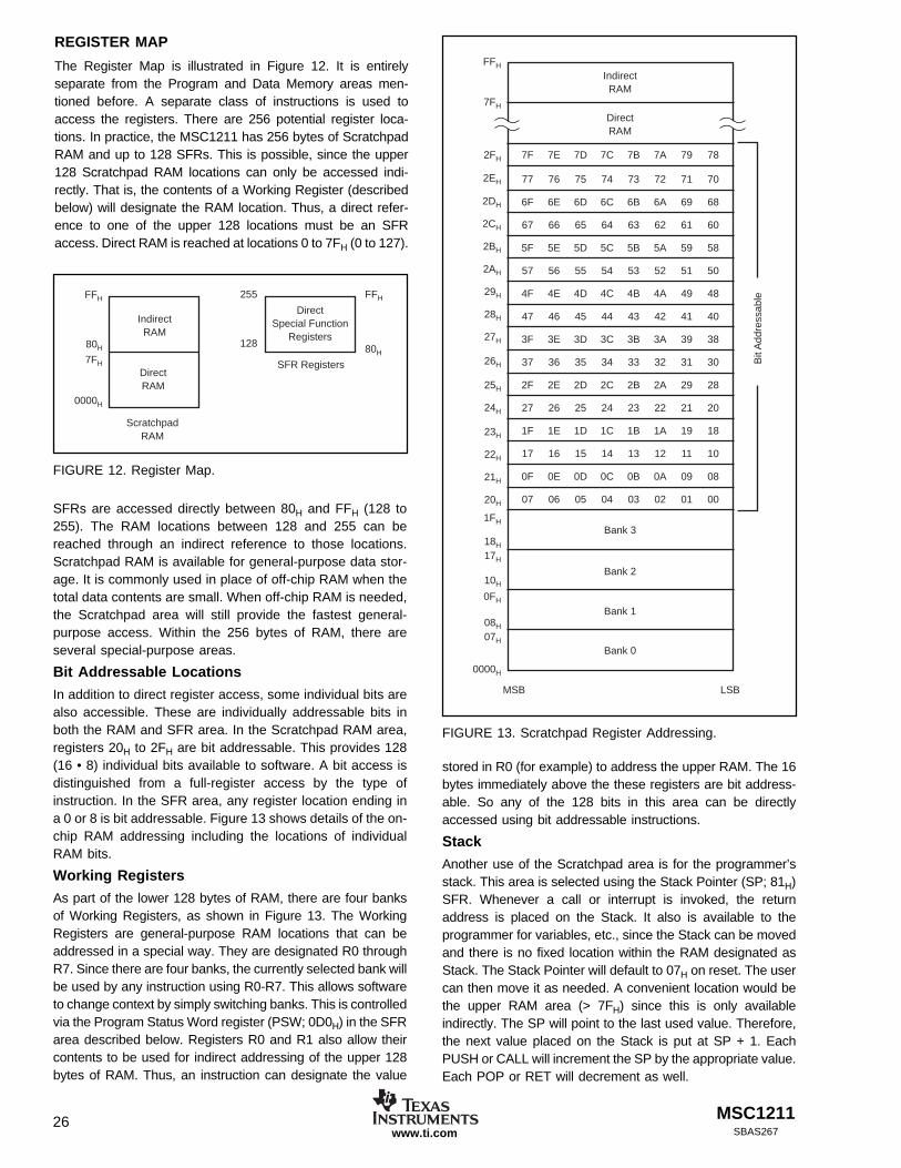
FIGURE 13. Scratchpad Register Addressing.
REGISTER MAP
The Register Map is illustrated in Figure 12. It is entirelyseparate from the Program and Data Memory areas men-tioned before. A separate class of instructions is used toaccess the registers. There are 256 potential register loca-tions. In practice, the MSC1211 has 256 bytes of ScratchpadRAM and up to 128 SFRs. This is possible, since the upper128 Scratchpad RAM locations can only be accessed indi-rectly. That is, the contents of a Working Register (describedbelow) will designate the RAM location. Thus, a direct refer-ence to one of the upper 128 locations must be an SFRaccess. Direct RAM is reached at locations 0 to 7FH (0 to 127).
FFH
7FH
2FH
2DH
2EH
2CH
2BH
2AH
29H
28H
27H
26H
25H
24H
23H
22H
21H
20H
1FH
18H
17H
10H
0FH
08H
07H
7F 7E 7D 7C 7B 7A 79 78
77 76 75 74 73 72 71 70
6F 6E 6D 6C 6B 6A 69 68
67 66 65 64 63 62 61 60
5F 5E 5D 5C 5B 5A 59 58
57 56 55 54 53 52 51 50
4F 4E 4D 4C 4B 4A 49 48
47 46 45 44 43 42 41 40
3F 3E 3D 3C 3B 3A 39 38
37 36 35 34 33 32 31 30
2F 2E 2D 2C 2B 2A 29 28
27 26 25 24 23 22 21 20
1F 1E 1D 1C 1B 1A 19 18
17 16 15 14 13 12 11 10
0F 0E 0D 0C 0B 0A 09 08
07 06 05 04 03 02 01 00
0000H
DirectRAM
Bank 3
Bit
Add
ress
able
Bank 2
Bank 1
Bank 0
MSB LSB
IndirectRAM
FIGURE 12. Register Map.
FFH 255
128
FFH
80H80H
7FH
0000H
IndirectRAM
DirectRAM
ScratchpadRAM
SFR Registers
DirectSpecial Function
Registers
SFRs are accessed directly between 80H and FFH (128 to255). The RAM locations between 128 and 255 can bereached through an indirect reference to those locations.Scratchpad RAM is available for general-purpose data stor-age. It is commonly used in place of off-chip RAM when thetotal data contents are small. When off-chip RAM is needed,the Scratchpad area will still provide the fastest general-purpose access. Within the 256 bytes of RAM, there areseveral special-purpose areas.
Bit Addressable Locations
In addition to direct register access, some individual bits arealso accessible. These are individually addressable bits inboth the RAM and SFR area. In the Scratchpad RAM area,registers 20H to 2FH are bit addressable. This provides 128(16 • 8) individual bits available to software. A bit access isdistinguished from a full-register access by the type ofinstruction. In the SFR area, any register location ending ina 0 or 8 is bit addressable. Figure 13 shows details of the on-chip RAM addressing including the locations of individualRAM bits.
Working Registers
As part of the lower 128 bytes of RAM, there are four banksof Working Registers, as shown in Figure 13. The WorkingRegisters are general-purpose RAM locations that can beaddressed in a special way. They are designated R0 throughR7. Since there are four banks, the currently selected bank willbe used by any instruction using R0-R7. This allows softwareto change context by simply switching banks. This is controlledvia the Program Status Word register (PSW; 0D0H) in the SFRarea described below. Registers R0 and R1 also allow theircontents to be used for indirect addressing of the upper 128bytes of RAM. Thus, an instruction can designate the value
stored in R0 (for example) to address the upper RAM. The 16bytes immediately above the these registers are bit address-able. So any of the 128 bits in this area can be directlyaccessed using bit addressable instructions.
Stack
Another use of the Scratchpad area is for the programmer’sstack. This area is selected using the Stack Pointer (SP; 81H)SFR. Whenever a call or interrupt is invoked, the returnaddress is placed on the Stack. It also is available to theprogrammer for variables, etc., since the Stack can be movedand there is no fixed location within the RAM designated asStack. The Stack Pointer will default to 07H on reset. The usercan then move it as needed. A convenient location would bethe upper RAM area (> 7FH) since this is only availableindirectly. The SP will point to the last used value. Therefore,the next value placed on the Stack is put at SP + 1. EachPUSH or CALL will increment the SP by the appropriate value.Each POP or RET will decrement as well.
MSC1211 27SBAS267 www.ti.com
If an 8-bit address is being used (MOVX @RI), the contentsof the MPAGE (92H) SFR remain at the Port 2 pins through-out the external memory cycle. This will facilitate paging.
In any case, the low byte of the address is time-multiplexedwith the data byte on Port 0. The ADDR/DATA signals useCMOS drivers in the Port 0, Port 2, WR, and RD outputbuffers. Thus, in this application the Port 0 pins are not open-drain outputs, and do not require external pull-ups for high-speed access. Signal ALE (Address Latch Enable) should beused to capture the address byte into an external latch. Theaddress byte is valid at the negative transition of ALE. Then,in a write cycle, the data byte to be written appears on Port 0just before WR is activated, and remains there until after WRis deactivated. In a read cycle, the incoming byte is acceptedat Port 0 just before the read strobe is deactivated.
The function of Port 0 and Port 2 is selected in HardwareConfiguration Register 1. This can only be changed during theFlash Program mode. There is no conflict in the use of theseregisters; they will either be used as general-purpose I/O or forexternal memory access. The default state is for Port 0 and Port2 to be used as general-purpose I/O. If an external memoryaccess is attempted when they are configured as general-purpose I/O, the values of Port 0 and Port 2 will not be affected.
External Program Memory is accessed under two conditions:
1) Whenever signal EA is LOW during reset, then all futureaccesses are external, or
2) Whenever the Program Counter (PC) contains a numberthat is outside of the internal Program Memory address range,if the ports are enabled.
If Port 0 and Port 2 is selected for external memory, all 8 bitsof Port 0 and Port 2, as well as P3.6 and P3.7, are dedicatedto an output function and may not be used for general-purpose I/O. During external program fetches, Port 2 outputsthe high byte of the PC.
Programming Flash Memory
There are four sections of Flash Memory for programming.
1. 128 configuration bytes.
2. Reset sector (4kB) (not to be confused with the 2kB BootROM).
3. Program Memory.
4. Data Memory.
Boot Rom
There is a 2kB Boot ROM that controls operation during serialor parallel programming. Additionally, the Boot ROM routinescan be accessed during the user mode if it is enabled. Whenenabled, the Boot ROM routines will be located at memoryaddresses F800H-FFFFH during user mode. In program modethe Boot ROM is located in the first 2kB of Program Memory.
Program Memory
After reset, the CPU begins execution from Program Memorylocation 0000H. The selection of where Program Memory ex-ecution begins is made by tying the EA pin to VDD for internalaccess, or DGND for external access. When EA is tied to VDD,any PC fetches outside the internal Program Memory addressoccur from external memory. If EA is tied to DGND, then all PCfetches address external memory. The standard internal Pro-gram Memory size for MSC1211 family members is shown inTable VIII. Refer to the Accessing External Memory section fordetails on using external Program Memory. If enabled the BootROM will appear from address F800H to FFFFH.
STANDARD INTERNALMODEL NUMBER PROGRAM MEMORY SIZE (BYTES)
MSC1211Y5 32kMSC1211Y4 16kMSC1211Y3 8kMSC1211Y2 4k
TABLE VIII. MSC1211 Maximum Internal Program Memory Sizes.
ACCESSING EXTERNAL MEMORY
If external memory is used, P0 and P2 can be configured asaddress and data lines. If external memory is not used, P0and P2 can be configured as general-purpose I/O linesthrough the Hardware Configuration Register.
To enable access to external memory bits 0 and 1 of theHCR1 register must be set to 0. When these bits are enabledall memory accesses for both internal and external memorywill appear on ports 0 and 2. During the data portion of thecycle for internal memory, Port 0 will be zero for securitypurposes.
Accesses to external memory are of two types: accesses toexternal Program Memory and accesses to external DataMemory. Accesses to external Program Memory use signalPSEN (program store enable) as the read strobe. Accessesto external Data Memory use RD or WR (alternate functionsof P3.7 and P3.6) to strobe the memory.
External Program Memory and external Data Memory maybe combined if desired by applying the RD and PSENsignals to the inputs of an AND gate and using the output ofthe gate as the read strobe to the external Program/DataMemory.
A program fetch from external Program Memory uses a 16-bit address. Accesses to external Data Memory can useeither a 16-bit address (MOVX @DPTR) or an 8-bit address(MOVX @RI).
If Port 2 is selected for external memory use (HCR1, bit 0), it cannot be used as a general-purpose I/O. This bit (or Bit 1 of HCR1)also forces bits P3.6 and P3.7 to be used for WR and RD insteadof I/O. Port 2, P3.6, and P3.7 should all be written to ‘1’.

MSC121128SBAS267www.ti.com
PRIORITYINTERRUPT/EVENT ADDR NUM PRIORITY FLAG ENABLE CONTROL
DVDD Low Voltage/HW Breakpoint 33H 6 HIGH EDLVB (AIE.0)(1) EDLVV (AIE.0)(1) N/A0 EBP (BPCON.0)(1) EBP (BPCON.0)(1)
AVDD Low Voltage 33H 6 0 EALV (AIE.1)(1) EALV (AIE.1)(1) N/A
SPI Receive / I2C 33H 6 0 ESPIR (AIE.2)(1) ESPIR (AIE.2)(1) N/A
SPI Transmit 33H 6 0 ESPIT (AIE.3)(1) ESPIT (AIE.3)(1) N/A
Milliseconds Timer 33H 6 0 EMSEC (AIE.4)(1) EMSEC (AIE.4)(1) N/A
ADC 33H 6 0 EADC (AIE.5)(1) EADC (AIE .5)(1) N/A
Summation Register 33H 6 0 ESUM (AIE.6)(1) ESUM (AIE.6)(1) N/A
Seconds Timer 33H 6 0 ESEC (AIE.7)(1) ESEC (AIE.7)(1) N/A
External Interrupt 0 03H 0 1 IE0 (TCON.1)(2) EX0 (IE.0)(4) PX0 (IP.0)
Timer 0 Overflow 0BH 1 2 TF0 (TCON.5)(3) ET0 (IE.1)(4) PT0 (IP.1)
External Interrupt 1 13H 2 3 IE1 (TCON.3)(2) EX1 (IE.2)(4) PX1 (IP.2)
Timer 1 Overflow 1BH 3 4 TF1 (TCON.7)(3) ET1 (IE.3)(4) PT1 (IP.3)
Serial Port 0 23H 4 5 RI_0 (SCON0.0) ES0 (IE.4)(4) PS0 (IP.4)TI_0 (SCON0.1)
Timer 2 Overflow 2BH 5 6 TF2 (T2CON.7) ET2 (IE.5)(4) PT2 (IP.5)
Serial Port 1 3BH 7 7 RI_1 (SCON1.0) ES1 (IE.6)(4) PS1 (IP.6)TI_1 (SCON1.1)
External Interrupt 2 43H 8 8 IE2 (EXIF.4) EX2 (EIE.0)(4) PX2 (IP.0)
External Interrupt 3 4BH 9 9 IE3 (EXIF.5) EX3 (EIE.1)(4) PX3 (IP.1)
External Interrupt 4 53H 10 10 IE4 (EXIF.6) EX4 (EIE.2)(4) PX4 (IP.2)
External Interrupt 5 5BH 11 11 IE5 (EXIF.7) EX5 (EIE.3)(4) PX5 (IP.3)
Watchdog 63H 12 12 WDTI (EICON.3) EWDI (EIE.4)(4) PWDI (IP.4)LOW
NOTES: (1) These interrupts set the AI flag (EICON.4) and are enabled by EAI (EICON.5). (2) If edge triggered, cleared automatically by hardware when theservice routine is vectored to. If level triggered, the flag follows the state of the pin. (3) Cleared automatically by hardware when interrupt vector occurs.(4) Globally enabled by EA (IE.7).
TABLE IX. Interrupt Summary.
INTERRUPT
FIGURE 14. Parallel Programming Configuration.
PSEN
ALE
MSC1211 HOST
FlashProgrammer
P2[7]
P2[6:0]
P1[7:0]
P0[7:0]
P3[7:5]
P3[4]
P3[3]
P3[2]
RST
XIN
PSEL
AddrHi[6:0]
AddrLo[7:0]
Data[7:0]
Cmd[2:0]
Req
Ack
Pass
RST
CLK
NC
operate in normal user mode. Both signals LOW is a reservedmode and is not defined. Programming mode is exited with apower-on reset signal and the normal mode selected.
The MSC1211 is shipped with Flash Memory erased (all 1’s).Parallel programming methods typically involve a third-partyprogrammer. Serial programming methods typically involve in-system programming. User Application mode allows FlashProgram and Data Memory programming. The actual code forFlash programming can not execute from Flash. That code mustexecute from the Boot ROM or internal (von Neumann) RAM.
INTERRUPTS
The MSC1211 uses a three-priority interrupt system. Asshown in Table IX, each interrupt source has an independentpriority bit, flag, interrupt vector, and enable (except that nineinterrupts share the Auxilliary Interrupt (AI) at the highestpriority). In addition, interrupts can be globally enabled ordisabled. The interrupt structure is compatible with the origi-nal 8051 family. All of the standard interrupts are available.
HARDWARE CONFIGURATION MEMORY
The 128 configuration bytes can only be written during theprogram mode. The bytes are accessed through SFR regis-ters CADDR (SFR 93H) and CDATA (SFR 94H). Two of theconfiguration bytes control Flash partitioning and systemcontrol. If the security bit is set, these bits can not be changedexcept with a Mass Erase command that erases all of theFlash Memory including the 128 configuration bytes.
Flash Programming Mode
There are two programming modes: parallel and serial. Theprogramming mode is selected by the state of the ALE andPSEN signals during power-on reset. Serial programmingmode is selected with PSEN = 0 and ALE = 1. Parallelprogramming mode is selected with PSEN = 1 and ALE = 0(see Figure 14). If they are both HIGH, the MSC1211 will

MSC1211 29SBAS267 www.ti.com
Hardware Configuration Register 0 (HCR0)—Accessed Using SFR Registers CADDR and CDATA.
For access to this register during normal operation, refer to the register descriptions for CADDR and CDATA.
EPMA Enable Programming Memory Access (Security Bit).
bit 7 0: After reset in programming modes, Flash Memory can only be accessed in UAM mode until a mass erase is done.
1: Fully Accessible (default)
PML Program Memory Lock. (PML has Priority Over RSL)
bit 6 0: Enable all Flash Programming Modes in program mode, can be written in UAM.
1: Enable read only for program mode, can’t be written in UAM (default).
RSL Reset Sector Lock.
bit 5 0: Enable Reset Sector Writing
1: Enable Read Only Mode for Reset Sector (4kB) (default)
EBR Enable Boot Rom. Boot Rom is 2kB of code located in ROM, not to be confused with the 4kB Boot Sector locatedin Flash Memory.
bit 4 0: Disable Internal Boot Rom
1: Enable Internal Boot Rom (default)
EWDR Enable Watchdog Reset.
bit 3 0: Disable Watchdog Reset
1: Enable Watchdog Reset (default)
DFSEL Data Flash Memory Size. (see Table III)
bits 2-0 000: Reserved
001: 32kB, 16kB, 8kB, or 4kB Data Flash Memory
010: 16kB, 8kB, or 4kB Data Flash Memory
011: 8kB or 4kB Data Flash Memory
100: 4kB Data Flash Memory
101: 2kB Data Flash Memory
110: 1kB Data Flash Memory
111: No Data Flash Memory (default)
The reset sector can be used to provide another method of Flash Memory programming. This will allow Program Memoryupdates without changing the jumpers for in-circuit code updates or program development. The code in this boot sector wouldthen provide the monitor and programming routines with the ability to jump into the main Flash code when programming isfinished.
bit 7 bit 6 bit 5 bit 4 bit 3 bit 2 bit 1 bit 0
CADDR 7FH EPMA PML RSL EBR EWDR DFSEL2 DFSEL1 DFSEL0

MSC121130SBAS267www.ti.com
For access to this register during normal operation, refer to the register descriptions for CADDR and CDATA.
DBLSEL Digital Brownout Level Select
bits 7-6 00: 4.5V
01: 4.2V
10: 2.7V
11: 2.5V (default)
ABLSEL Analog Brownout Level Select
bits 5-4 00: 4.5V
01: 4.2V
10: 2.7V
11: 2.5V (default)
DAB Disable Analog Power-Supply Brownout Detection
bit 3 0: Enable Analog Brownout Detection
1: Disable Analog Brownout Detection (default).
DDB Disable Digital Power-Supply Brownout Detection
bit 2 0: Enable Digital Brownout Detection
1: Disable Digital Brownout Detection (default)
EGP0 Enable General-Purpose I/O for Port 0
bit 1 0: Port 0 is Used for External Memory, P3.6 and P3.7 Used for WR and RD.
1: Port 0 is Used as General-Purpose I/O (default)
EGP23 Enable General-Purpose I/O for Ports 2 and 3
bit 0 0: Port 2 is Used for External Memory, P3.6 and P3.7 Used for WR and RD.
1: Port 2 and Port3 are Used as General-Purpose I/O (default)
Configuration Memory Programming
Certain key functions such as Brownout Reset and Watchdog Timer are controlled by the hardware configuration bits. Thesebits are nonvolatile and can only be changed through serial and parallel programming. Other peripheral control and statusfunctions, such as ADC configuration timer setup, and Flash control are controlled through the SFRs.
7 6 5 4 3 2 1 0
CADDR 7EH DBLSEL1 DBLSEL0 ABLSEL1 ABLSEL0 DAB DDB EGP0 EGP23
Hardware Configuration Register 1 (HCR1)

MSC1211 31SBAS267 www.ti.com
SFR Definitions (Boldface is unique to the MSC1211)
ADDRESS REGISTER BIT 7 BIT 6 BIT 5 BIT 4 BIT 3 BIT 2 BIT 1 BIT 0 RESET VALUES
80H P0 P0.7 P0.6 P0.5 P0.4 P0.3 P0.2 P0.1 P0.0 FFH
81H SP 07H
82H DPL0 00H
83H DPH0 00H
84H DPL1 00H
85H DPH1 00H
86H DPS 0 0 0 0 0 0 0 SEL 00H
87H PCON SMOD 0 1 1 GF1 GF0 STOP IDLE 30H
88H TCON TF1 TR1 TF0 TR0 IE1 IT1 IE0 IT0 00H
89H TMOD |---------------------------Timer 1 --------------------------| |--------------------------Timer 0 ---------------------------| 00H
GATE C/T M1 M0 GATE C/T M1 M08AH TL0 00H
8BH TL1 00H
8CH TH0 00H
8DH TH1 00H
8EH CKCON 0 0 T2M T1M T0M MD2 MD1 MD0 01H
8FH MWS 0 0 0 0 0 0 0 MXWS 00H
90H P1 P1.7 P1.6 P1.5 P1.4 P1.3 P1.2 P1.1 P1.0 FFH
INT5/SCLK/SCK INT4/MISO/SDA INT3/MOSI INT2/SS TXD1 RXD1 T2EX T291H EXIF IE5 IE4 IE3 IE2 1 0 0 0 08H
92H MPAGE 00H
93H CADDR 00H
94H CDATA 00H
95H MCON BPSEL 0 0 RAMMAP 00H
96H
97H
98H SCON0 SM0_0 SM1_0 SM2_0 REN_0 TB8_0 RB8_0 TI_0 RI_0 00H
99H SBUF0 00H
9AH SPICON SCLK2 SCLK1 SCLK0 FIFO ORDER MSTR CPHA CPOL 00HI2CCON START STOP ACK 0 FAST MSTR SCLS FILEN
9BH SPIDATA 00H
I2CDATA9CH SPIRCON RXCNT7 RXCNT6 RXCNT5 RXCNT4 RXCNT3 RXCNT2 RXCNT1 RXCNT0 00H
RXFLUSH RXIRQ2 RXIRQ1 RXIRQ0I2CSTAT GCMEN
9DH SPITCON TXCNT7 TXCNT6 TXCNT5 TXCNT4 TXCNT3 TXCNT2 TXCNT1 TXCNT0 00HTXFLUSH CLK_EN DRV_DLY DRV_EN TXIRQ2 TXIRQ1 TXIRQ0
I2CGM STAT7 STAT6 STAT5 STAT4 STAT3 0 0 0SCKD7/SAE SCKD6/SA6 SCKD5/SA5 SCKD4/SA4 SCKD3/SA3 SCKD2/SA2 SCKD1/SA1 SCKD0/SA0
9EH SPISTART 1 80H
9FH SPIEND 1 80H
A0H P2 P2.7 P2.6 P2.5 P2.4 P2.3 P2.2 P2.1 P2.0 FFH
A1H PWMCON PPOL PWMSEL SPDSEL TPCNTL2 TPCNTL1 TPCNTL0 00H
A2H PWMLOW PWM7 PWM6 PWM5 PWM4 PWM3 PWM2 PWM1 PWM0 00HTONELOW TDIV7 TDIV6 TDIV5 TDIV4 TDIV3 TDIV2 TDIV1 TDIV0
A3H PWMHI PWM15 PWM14 PWM13 PWM12 PWM11 PWM10 PWM9 PWM8 00HTONEHI TDIV15 TDIV14 TDIV13 TDIV12 TDIV11 TDIV10 TDIV9 TDIV8
A4H
A5H PAI 0 0 0 0 PAI3 PAI2 PAI1 PAI0 00H
A6H AIE ESEC ESUM EADC EMSEC ESPIT ESPIR/EI2C EALV EDLVB 00H
A7H AISTAT SEC SUM ADC MSEC SPIT SPIR/I2CSI ALVD DLVD 00H
A8H IE EA ES1 ET2 ES0 ET1 EX1 ET0 EX0 00H
A9H BPCON BP 0 0 0 0 0 PMSEL EBP 00H
AAH BPLABH BPHACH P0DDRL P03H P03L P02H P02L P01H P01L P00H P00L 00H
ADH P0DDRH P07H P07L P06H P06L P05H P05L P04H P04L 00H
AEH P1DDRL P13H P13L P12H P12L P11H P11L P10H P10L 00H
AFH P1DDRH P17H P17L P16H P16L P15H P15L P14H P14L 00H
B0H P3 P3.7 P3.6 P3.5 P3.4 P3.3 P3.2 P3.1 P3.0 FFH
RD WR T1 T0 INT1 INT0 TXD0 RXD0B1H P2DDRL P23H P23L P22H P22L P21H P21L P20H P20L 00H
B2H P2DDRH P27H P27L P26H P26L P25H P25L P24H P24L 00H
B3H P3DDRL P33H P33L P32H P32L P31H P31L P30H P30L 00H
B4H P3DDRH P37H P37L P36H P36L P35H P35L P34H P34L 00H
B5H DACLB6H DACHB7H DACCON DSEL7 DSEL6 DSEL5 DSEL4 DSEL3 DSEL2 DSEL1 DSEL0 00H
B8H IP 1 PS1 PT2 PS0 PT1 PX1 PT0 PX0 80H

MSC121132SBAS267www.ti.com
B9H
BAH
BBH
BCH
BDH
BEH
BFH
C0H SCON1 SM0_1 SM1_1 SM2_1 REN_1 TB8_1 RB8_1 TI_1 RI_1 00H
C1H SBUF1 00H
C2H
C3H
C4H
C5H
C6H EWU EWUWDT EWUEX1 EWUEX0 00H
C7H SYSCLK 0 0 DIVMOD1 DIVMOD0 0 DIV2 DIV1 DIV0 00H
C8H T2CON TF2 EXF2 RCLK TCLK EXEN2 TR2 C/T2 CP/RL2 00H
C9H
CAH RCAP2L 00H
CBH RCAP2H 00H
CCH TL2 00H
CDH TH2 00H
CEH
CFH
D0H PSW CY AC F0 RS1 RS0 OV F1 P 00H
D1H OCL LSB 00H
D2H OCM 00H
D3H OCH MSB 00H
D4H GCL LSB 24H
D5H GCM 90H
D6H GCH MSB 67H
D7H ADMUX INP3 INP2 INP1 INP0 INN3 INN2 INN1 INN0 01H
D8H EICON SMOD1 1 EAI AI WDTI 0 0 0 40H
D9H ADRESL LSB 00H
DAH ADRESM 00H
DBH ADRESH MSB 00H
DCH ADCON0 — BOD EVREF VREFH EBUF PGA2 PGA1 PGA0 38H
DDH ADCON1 — POL SM1 SM0 — CAL2 CAL1 CAL0 x000_0000B
DEH ADCON2 DR7 DR6 DR5 DR4 DR3 DR2 DR1 DR0 1BH
DFH ADCON3 0 0 0 0 0 DR10 DR9 DR8 06H
E0H ACC 00H
E1H SSCON SSCON1 SSCON0 SCNT2 SCNT1 SCNT0 SHF2 SHF1 SHF0 00H
E2H SUMR0 00H
E3H SUMR1 00H
E4H SUMR2 00H
E5H SUMR3 00H
E6H ODAC 00H
E7H LVDCON ALVDIS ALVD2 ALVD1 ALVD0 DLVDIS DLVD2 DLVD1 DLVD0 00H
E8H EIE 1 1 1 EWDI EX5 EX4 EX3 EX2 E0H
E9H HWPC0 1 MEMORY SIZE 0000_01xxB
EAH HWPC1 1 08H
EBH HWVERECH Reserved 00H
EDH Reserved 00H
EEH FMCON 0 PGERA 0 FRCM 0 BUSY 1 0 02H
EFH FTCON FER3 FER2 FER1 FER0 FWR3 FWR2 FWR1 FWR0 A5H
F0H B 00H
F1H PDCON 0 PDDAC PDI2C PDPWM PDAD PDWDT PDST PDSPI 7FH
F2H PASEL 0 0 PSEN2 PSEN1 PSEN0 0 ALE1 ALE0 00H
F3H
F4H
F5H
F6H ACLK 0 FREQ6 FREQ5 FREQ4 FREQ3 FREQ2 FREQ1 FREQ0 03H
F7H SRST 0 0 0 0 0 0 0 RSTREQ 00H
F8H EIP 1 1 1 PWDI PX5 PX4 PX3 PX2 E0H
F9H SECINT WRT SECINT6 SECINT5 SECINT4 SECINT3 SECINT2 SECINT1 SECINT0 7FH
FAH MSINT WRT MSINT6 MSINT5 MSINT4 MSINT3 MSINT2 MSINT1 MSINT0 7FH
FBH USEC 0 0 FREQ5 FREQ4 FREQ3 FREQ2 FREQ1 FREQ0 03H
FCH MSECL 9FH
FDH MSECH 0FH
FEH HMSEC 63H
FFH WDTCON EWDT DWDT RWDT WDCNT4 WDCNT3 WDCNT2 WDCNT1 WDCNT0 00H
ADDRESS REGISTER BIT 7 BIT 6 BIT 5 BIT 4 BIT 3 BIT 2 BIT 1 BIT 0 RESET VALUES

MSC1211 33SBAS267 www.ti.com
7 6 5 4 3 2 1 0 Reset Value
SFR 81H SP.7 SP.6 SP.5 SP.4 SP.3 SP.2 SP.1 SP.0 07H
7 6 5 4 3 2 1 0 Reset Value
SFR 80H P0.7 P0.6 P0.5 P0.4 P0.3 P0.2 P0.1 P0.0 FFH
SP.7-0 Stack Pointer. The stack pointer identifies the location where the stack will begin. The stack pointer is incremented beforebits 7-0 every PUSH or CALL operation and decremented after each POP or RET/RETI. This register defaults to 07H after reset.
Data Pointer Low 0 (DPL0)
Port 0 (P0)
P0.7-0 Port 0. This port functions as a multiplexed address/data bus during external memory access, and as a general-bits 7-0 purpose I/O port when external memory access is not needed. During external memory cycles, this port will contain
the LSB of the address when ALE is HIGH, and Data when ALE is LOW. When used as a general-purpose I/O, thisport drive is selected by P0DDRL and P0DDRH (ACH, ADH). Whether Port 0 is used as general-purpose I/O or forexternal memory access is determined by the Flash Configuration Register (HCR1.1) (see SFR CADDR 93H).
Stack Pointer (SP)
DPL0.7-0 Data Pointer Low 0. This register is the low byte of the standard 8051 16-bit data pointer. DPL0 and DPH0bits 7-0 are used to point to non-scratchpad data RAM. The current data pointer is selected by DPS (SFR 86H).
Data Pointer High 0 (DPH0)
7 6 5 4 3 2 1 0 Reset Value
SFR 82H DPL0.7 DPL0.6 DPL0.5 DPL0.4 DPL0.3 DPL0.2 DPL0.1 DPL0.0 00H
DPH0.7-0 Data Pointer High 0. This register is the high byte of the standard 8051 16-bit data pointer. DPL0 and DPH0bits 7-0 are used to point to non-scratchpad data RAM. The current data pointer is selected by DPS (SFR 86H).
Data Pointer Low 1 (DPL1)
7 6 5 4 3 2 1 0 Reset Value
SFR 83H DPH0.7 DPH0.6 DPH0.5 DPH0.4 DPH0.3 DPH0.2 DPH0.1 DPH0.0 00H
DPL1.7-0 Data Pointer Low 1. This register is the low byte of the auxiliary 16-bit data pointer. When the SEL bit (DPS.0)bits 7-0 (SFR 86H) is set, DPL1 and DPH1 are used in place of DPL0 and DPH0 during DPTR operations.
Data Pointer High 1 (DPH1)
7 6 5 4 3 2 1 0 Reset Value
SFR 84H DPL1.7 DPL1.6 DPL1.5 DPL1.4 DPL1.3 DPL1.2 DPL1.1 DPL1.0 00H
DPH1.7-0 Data Pointer High. This register is the high byte of the auxiliary 16-bit data pointer. When the SEL bit (DPS.0)bits 7-0 (SFR 86H) is set, DPL1 and DPH1 are used in place of DPL0 and DPH0 during DPTR operations.
Data Pointer Select (DPS)
7 6 5 4 3 2 1 0 Reset Value
SFR 85H DPH1.7 DPH1.6 DPH1.5 DPH1.4 DPH1.3 DPH1.2 DPH1.1 DPH1.0 00H
7 6 5 4 3 2 1 0 Reset Value
SFR 86H 0 0 0 0 0 0 0 SEL 00H
SEL Data Pointer Select. This bit selects the active data pointer.
bit 0 0: Instructions that use the DPTR will use DPL0 and DPH0.1: Instructions that use the DPTR will use DPL1 and DPH1.

MSC121134SBAS267www.ti.com
SMOD Serial Port 0 Baud Rate Doubler Enable. The serial baud rate doubling function for Serial Port 0.bit 7 0: Serial Port 0 baud rate will be a standard baud rate.
1: Serial Port 0 baud rate will be double that defined by baud rate generation equation.
GF1 General-Purpose User Flag 1. This is a general-purpose flag for software control.bit 3
GF0 General-Purpose User Flag 0. This is a general-purpose flag for software control.bit 2
STOP Stop Mode Select. Setting this bit will halt the oscillator and block external clocks. This bit will always read as a 0.bit 1 Exit with RESET.
IDLE Idle Mode Select. Setting this bit will freeze the CPU, Timer 0, 1, and 2, and the UARTs; other peripherals remainbit 0 active. This bit will always be read as a 0. Exit with AI (A6H) and EWU (C6H) interrupts.
Timer/Counter Control (TCON)
7 6 5 4 3 2 1 0 Reset Value
SFR 87H SMOD 0 1 1 GF1 GF0 STOP IDLE 30H
TF1 Timer 1 Overflow Flag. This bit indicates when Timer 1 overflows its maximum count as defined by the currentbit 7 mode. This bit can be cleared by software and is automatically cleared when the CPU vectors to the Timer 1
interrupt service routine.0: No Timer 1 overflow has been detected.1: Timer 1 has overflowed its maximum count.
TR1 Timer 1 Run Control. This bit enables/disables the operation of Timer 1. Halting this timer will preserve thecurrent bit 6 count in TH1, TL1.0: Timer is halted.1: Timer is enabled.
TF0 Timer 0 Overflow Flag. This bit indicates when Timer 0 overflows its maximum count as defined by the currentbit 5 mode. This bit can be cleared by software and is automatically cleared when the CPU vectors to the Timer 0
interrupt service routine.0: No Timer 0 overflow has been detected.1: Timer 0 has overflowed its maximum count.
TR0 Timer 0 Run Control. This bit enables/disables the operation of Timer 0. Halting this timer will preserve thebit 4 current count in TH0, TL0.
0: Timer is halted.1: Timer is enabled.
IE1 Interrupt 1 Edge Detect. This bit is set when an edge/level of the type defined by IT1 is detected. If IT1 = 1, thisbit 3 bit will remain set until cleared in software or the start of the External Interrupt 1 service routine. If IT1 = 0, this
bit will inversely reflect the state of the INT1 pin.
IT1 Interrupt 1 Type Select. This bit selects whether the INT1 pin will detect edge or level triggered interrupts.bit 2 0: INT1 is level triggered.
1: INT1 is edge triggered.
IE0 Interrupt 0 Edge Detect. This bit is set when an edge/level of the type defined by IT0 is detected. If IT0 = 1, thisbit 3 bit will remain set until cleared in software or the start of the External Interrupt 0 service routine. If IT0 = 0, this
bit will inversely reflect the state of the INT0 pin.
IT0 Interrupt 0 Type Select. This bit selects whether the INT0 pin will detect edge or level triggered interrupts.bit 2 0: INT0 is level triggered.
1: INT0 is edge triggered.
Power Control (PCON)
7 6 5 4 3 2 1 0 Reset Value
SFR 88H TF1 TR1 TF0 TR0 IE1 IT1 IE0 IT0 00H

MSC1211 35SBAS267 www.ti.com
Timer Mode Control (TMOD)
7 6 5 4 3 2 1 0TIMER 1 TIMER 0 Reset Value
SFR 89H GATE C/T M1 M0 GATE C/T M1 M0 00H
GATE Timer 1 Gate Control. This bit enables/disables the ability of Timer 1 to increment.bit 7 0: Timer 1 will clock when TR1 = 1, regardless of the state of pin INT1.
1: Timer 1 will clock only when TR1 = 1 and pin INT1 = 1.
C/T Timer 1 Counter/Timer Select.bit 6 0: Timer is incremented by internal clocks.
1: Timer is incremented by pulses on T1 pin when TR1 (TCON.6, SFR 88H) is 1.
M1, M0 Timer 1 Mode Select. These bits select the operating mode of Timer 1.bits 5-4
TL0.7-0 Timer 0 LSB. This register contains the least significant byte of Timer 0.
bits 7-0
Timer 1 LSB (TL1)
7 6 5 4 3 2 1 0 Reset Value
SFR 8AH TL0.7 TL0.6 TL0.5 TL0.4 TL0.3 TL0.2 TL0.1 TL0.0 00H
TL1.7-0 Timer 1 LSB. This register contains the least significant byte of Timer 1.
bits 7-0
Timer 0 MSB (TH0)
7 6 5 4 3 2 1 0 Reset Value
SFR 8BH TL1.7 TL1.6 TL1.5 TL1.4 TL1.3 TL1.2 TL1.1 TL1.0 00H
TH0.7-0 Timer 0 MSB. This register contains the most significant byte of Timer 0.
bits 7-0
7 6 5 4 3 2 1 0 Reset Value
SFR 8CH TH0.7 TH0.6 TH0.5 TH0.4 TH0.3 TH0.2 TH0.1 TH0.0 00H
GATE Timer 0 Gate Control. This bit enables/disables the ability of Timer 0 to increment.bit 3 0: Timer 0 will clock when TR0 = 1, regardless of the state of pin INT0 (software control).
1: Timer 0 will clock only when TR0 = 1 and pin INT0 = 1 (hardware control).
C/T Timer 0 Counter/Timer Select.bit 2 0: Timer is incremented by internal clocks.
1: Timer is incremented by pulses on pin T0 when TR0 (TCON.4, SFR 88H) is 1.
M1, M0 Timer 0 Mode Select. These bits select the operating mode of Timer 0.
bits 1-0
M1 M0 MODE
0 0 Mode 0: 8-bit counter with 5-bit prescale.0 1 Mode 1: 16 bits.1 0 Mode 2: 8-bit counter with auto reload.1 1 Mode 3: Timer 1 is halted, but holds its count.
M1 M0 MODE
0 0 Mode 0: 8-bit counter with 5-bit prescale.0 1 Mode 1: 16 bits.1 0 Mode 2: 8-bit counter with auto reload.1 1 Mode 3: Timer 1 is halted, but holds its count.
Timer 0 LSB (TL0)

MSC121136SBAS267www.ti.com
Timer 1 MSB (TH1)
7 6 5 4 3 2 1 0 Reset Value
SFR 8DH TH1.7 TH1.6 TH1.5 TH1.4 TH1.3 TH1.2 TH1.1 TH1.0 00H
7 6 5 4 3 2 1 0 Reset Value
SFR 8EH 0 0 T2M T1M T0M MD2 MD1 MD0 01H
TH1.7-0 Timer 1 MSB. This register contains the most significant byte of Timer 1.bits 7-0
Clock Control (CKCON)
T2M Timer 2 Clock Select. This bit controls the division of the system clock that drives Timer 2. This bit has no effectbit 5 when the timer is in baud rate generator or clock output modes. Clearing this bit to 0 maintains 8051
compatibility. This bit has no effect on instruction cycle timing.0: Timer 2 uses a divide by 12 of the crystal frequency.1: Timer 2 uses a divide by 4 of the crystal frequency.
T1M Timer 1 Clock Select. This bit controls the division of the system clock that drives Timer 1. Clearing this bit tobit 4 0 maintains 8051 compatibility. This bit has no effect on instruction cycle timing.
0: Timer 1 uses a divide by 12 of the crystal frequency.1: Timer 1 uses a divide by 4 of the crystal frequency.
T0M Timer 0 Clock Select. This bit controls the division of the system clock that drives Timer 0. Clearing this bit tobit 3 0 maintains 8051 compatibility. This bit has no effect on instruction cycle timing.
0: Timer 0 uses a divide by 12 of the crystal frequency.1: Timer 0 uses a divide by 4 of the crystal frequency.
MD2, MD1, MD0 Stretch MOVX Select 2-0. These bits select the time by which external MOVX cycles are to be stretched.bits 2-0 This allows slower memory or peripherals to be accessed without using ports or manual software
intervention. The for RD or WR strobe will be stretched by the specified interval, which will be transparentto the software except for the increased time to execute the MOVX instruction. All internal MOVXinstructions on devices containing MOVX SRAM are performed at the 2 instruction cycle rate.
MXWS MOVX Write Select. This allows writing to the internal Flash program memory.bit 0 0: No writes are allowed to the internal Flash program memory.
1: Writing is allowed to the internal Flash program memory, unless PML (HCR0) or RSL (HCR0) are on.
7 6 5 4 3 2 1 0 Reset Value
SFR 8FH 0 0 0 0 0 0 0 MXWS 00H
RD or WR RD or WRSTROBE WIDTH STROBE WIDTH
MD2 MD1 MD0 STRETCH VALUE MOVX DURATION (SYS CLKs) (µs) AT 12MHz
0 0 0 0 2 Instruction Cycles 2 0.1670 0 1 1 3 Instruction Cycles (default) 4 0.3330 1 0 2 4 Instruction Cycles 8 0.6670 1 1 3 5 Instruction Cycles 12 1.0001 0 0 4 6 Instruction Cycles 16 1.3331 0 1 5 7 Instruction Cycles 20 1.6671 1 0 6 8 Instruction Cycles 24 2.0001 1 1 7 9 Instruction Cycles 28 2.333
Memory Write Select (MWS)

MSC1211 37SBAS267 www.ti.com
Port 1 (P1)7 6 5 4 3 2 1 0 Reset Value
SFR 90H P1.7 P1.6 P1.5 P1.4 P1.3 P1.2 P1.1 P1.0 FFH
INT5/SCLK/SCK INT4/MISO/SDA INT3/MOSI INT2/SS TXD1 RXD1 T2EX T2
P1.7-0 General-Purpose I/O Port 1. This register functions as a general-purpose I/O port. In addition, all the pins havebits 7-0 an alternative function listed below. Each of the functions is controlled by several other SFRs. The associated Port
1 latch bit must contain a logic ‘1’ before the pin can be used in its alternate function capacity. To use the alternatefunction, set the appropriate mode in P1DDRL (SFR AEH), P1DDRH (SFR AFH).
INT5/SCLK/SCK External Interrupt 5. A falling edge on this pin will cause an external interrupt 5 if enabled.bit 7 SPI Clock. The master clock for SPI data transfers.
Serial Clock. The serial clock for I2C data transfers.
INT4/MISO/SDA External Interrupt 4. A rising edge on this pin will cause an external interrupt 4 if enabled.bit 6 Master In Slave Out. For SPI data transfers, this pin receives data for the master and transmits data from the slave.
ISDA. For I2C data transfers, this pin is the data line.
INT3/MOSI External Interrupt 3. A falling edge on this pin will cause an external interrupt 3 if enabled.bit 5 Master Out Slave In. For SPI data transfers, this pin transmits master data and receives slave data.
INT2/SS External Interrupt 2. A rising edge on this pin will cause an external interrupt 2 if enabled.bit 4 Slave Select. During SPI operation, this pin provides the select signal for the slave device.
TXD1 Serial Port 1 Transmit. This pin transmits the serial Port 1 data in serial port modes 1, 2, 3, and emits thebit 3 synchronizing clock in serial port mode 0.
RXD1 Serial Port 1 Receive. This pin receives the serial Port 1 data in serial port modes 1, 2, 3, and is a bidirectionalbit 2 data transfer pin in serial port mode 0.
T2EX Timer 2 Capture/Reload Trigger. A 1 to 0 transition on this pin will cause the value in the T2 registers to bebit 1 transferred into the capture registers if enabled by EXEN2 (T2CON.3, SFR C8H). When in auto-reload mode, a 1 to 0
transition on this pin will reload the Timer 2 registers with the value in RCAP2L and RCAP2H if enabled byEXEN2 (T2CON.3, SFR C8H).
T2 Time 2 External Input. A 1 to 0 transition on this pin will cause Timer 2 to increment or decrement dependingbit 0 on the timer configuration.
External Interrupt Flag (EXIF)
7 6 5 4 3 2 1 0 Reset Value
SFR 91H IE5 IE4 IE3 IE2 1 0 0 0 08H
IE5 External Interrupt 5 Flag. This bit will be set when a falling edge is detected on INT5. This bit must bebit 7 cleared manually by software. Setting this bit in software will cause an interrupt if enabled.
IE4 External Interrupt 4 Flag. This bit will be set when a rising edge is detected on INT4. This bit must be clearedbit 6 manually by software. Setting this bit in software will cause an interrupt if enabled.
IE3 External Interrupt 3 Flag. This bit will be set when a falling edge is detected on INT3. This bit must be clearedbit 5 manually by software. Setting this bit in software will cause an interrupt if enabled.
IE2 External Interrupt 2 Flag. This bit will be set when a rising edge is detected on INT2. This bit must be clearedbit 4 manually by software. Setting this bit in software will cause an interrupt if enabled.
Memory Page (MPAGE)
7 6 5 4 3 2 1 0 Reset Value
SFR 92H 00H
MPAGE The 8051 uses Port 2 for the upper 8 bits of the external data memory access by MOVX A@RI and MOVX @RI,bits 7-0 A instructions. The MSC1211 uses register MPAGE instead of Port 2. To access external data memory using the
MOVX A@RI and MOVX @RI, A instructions, the user should preload the upper byte of the address into MPAGE (versuspreloading into P2 for the standard 8051).

MSC121138SBAS267www.ti.com
CADDR Configuration Address Register. This register supplies the address for reading bytes in the 128 bytes of Flash Configurationbits 7-0 Memory. WARNING: If this register is written to while executing from Flash Memory, the CDATA register will be incorrect.
Configuration Data Register (CDATA)
CDATA Configuration Data Register. This register will contain the data in the 128 bytes of Flash Configuration Memorybits 7-0 that is located at the last written address in the CADDR register. This is a read-only register.
Memory Control (MCON)
BPSEL Breakpoint Address Selectionbit 7 Write: Select one of two Breakpoint registers: 0 or 1.
0: Select breakpoint register 0.1: Select breakpoint register 1.Read: Provides the Breakpoint register that created the last interrupt: 0 or 1.
RAMMAP Memory Map 1kB extended SRAM.bit 0 0: Address is: 0000H-03FFH (default) (Data Memory)
1: Address is 8400H-87FFH (Data and Program Memory)
Serial Port 0 Control (SCON0)
7 6 5 4 3 2 1 0 Reset Value
SFR 94H 00H
7 6 5 4 3 2 1 0 Reset Value
SFR 95H BPSEL 0 0 — — — — RAMMAP 00H
SM0-2 Serial Port 0 Mode. These bits control the mode of serial Port 0. Modes 1, 2, and 3 have 1 start and 1 stop bitbits 7-5 in addition to the 8 or 9 data bits.
7 6 5 4 3 2 1 0 Reset Value
SFR 98H SM0_0 SM1_0 SM2_0 REN_0 TB8_0 RB8_0 TI_0 RI_0 00H
REN_0 Receive Enable. This bit enables/disables the serial Port 0 received shift register.bit 4 0: Serial Port 0 reception disabled.
1: Serial Port 0 received enabled (modes 1, 2, and 3). Initiate synchronous reception (mode 0).
TB8_0 9th Transmission Bit State. This bit defines the state of the 9th transmission bit in serial Port 0 modes 2 and 3.bit 3
RB8_0 9th Received Bit State. This bit identifies the state of the 9th reception bit of received data in serial Port 0 modesbit 2 2 and 3. In serial port mode 1, when SM2_0 = 0, RB8_0 is the state of the stop bit. RB8_0 is not used in mode 0.
TI_0 Transmitter Interrupt Flag. This bit indicates that data in the serial Port 0 buffer has been completely shiftedbit 1 out. In serial port mode 0, TI_0 is set at the end of the 8th data bit. In all other modes, this bit is set at the end
of the last data bit. This bit must be manually cleared by software.
MODE SM0 SM1 SM2 FUNCTION LENGTH PERIOD
0 0 0 0 Synchronous 8 bits 12 pCLK(1)
0 0 0 1 Synchronous 8 bits 4 pCLK(1)
1(2) 0 1 x Asynchronous 10 bits Timer 1 or 2 Baud Rate Equation
2 1 0 0 Asynchronous 11 bits 64 pCLK(1) (SMOD = 0)
32 pCLK(1) (SMOD = 1)
2 1 0 1 Asynchronous with 11 bits 64 pCLK(1) (SMOD = 0)
Multiprocessor Communication 32 pCLK(1) (SMOD = 1)
3(2) 1 1 0 Asynchronous 11 bits Timer 1 or 2 Baud Rate Equation3(2) 1 1 1 Asynchronous with 11 bits Timer 1 or 2 Baud Rate Equation
Multiprocessor Communication
NOTE: (1) pCLK will be equal to tCLK, except that pCLK will stop for IDLE. (2) For modes 1 and 3, the selection ofTimer 1 or 2 for baud rate is specified via the T2CON (C8H) register.
7 6 5 4 3 2 1 0 Reset Value
SFR 93H 00H
Configuration Address Register (CADDR) (write only)

MSC1211 39SBAS267 www.ti.com
RI_0 Receiver Interrupt Flag. This bit indicates that a byte of data has been received in the serial Port 0 buffer. Inbit 0 serial port mode 0, RI_0 is set at the end of the 8th bit. In serial port mode 1, RI_0 is set after the last sample
of the incoming stop bit subject to the state of SM2_0. In modes 2 and 3, RI_0 is set after the last sample ofRB8_0. This bit must be manually cleared by software.
Serial Data Buffer 0 (SBUF0)7 6 5 4 3 2 1 0 Reset Value
SFR 99H 00H
SBUF0 Serial Data Buffer 0. Data for Serial Port 0 is read from or written to this location. The serial transmit andbits 7-0 receive buffers are separate registers, but both are addressed at this location.
SPI Control (SPICON). Any change resets the SPI interface, counters, and pointers. PDCON controlswhich is enabled.
SCLK SCK Selection. Selection of tCLK divider for generation of SCK in Master mode.bits 7-5 SCLK2 SCLK1 SCLK0 SCK PERIOD
0 0 0 tCLK/20 0 1 tCLK/40 1 0 tCLK/80 1 1 tCLK/161 0 0 tCLK/321 0 1 tCLK/641 1 0 tCLK/1281 1 1 tCLK/256
START Start Condition (Master mode).bit 7 Read: Current status of start condition or repeated start condition.
Write: When operating as a master, a start condition is transmitted when the START bit is set to 1. During a datatransfer, if the START bit is set, a repeated start is transmitted after the current data transfer is complete.If no transfer is in progress when the START and STOP bits are set simultaneously, a START will befollowed by a STOP.
7 6 5 4 3 2 1 0 Reset Value
SFR 9AH SCLK2 SCLK1 SCLK0 FIFO ORDER MSTR CPHA CPOL 00H
7 6 5 4 3 2 1 0 Reset Value
SFR 9AH START STOP ACK 0 FAST MSTR SCLS FILEN 00H
FIFO Enable FIFO in on-chip indirect memory.bit 4 0: Both transmit and receive are double buffers
1: Circular FIFO used for transmit and receive bytes
ORDER Set Bit Order for Transmit and Receive.bit 3 0: Most Significant Bits First
1: Least Significant Bits First
MSTR SPI Master Mode.bit 2 0: Slave Mode
1: Master Mode
CPHA Serial Clock Phase Control.bit 1 0: Valid data starting from half SCK period before the first edge of SCK
1: Valid data starting from the first edge of SCK
CPOL Serial Clock Polarity.bit 0 0: SCK idle at logic LOW
1: SCK idle at logic HIGH
I2C Control Register (I2CCON)

MSC121140SBAS267www.ti.com
STOP Stop Condition (Master mode).bit 6 Read: Current status of stop condition.
Write: Setting STOP to logic 1 causes a stop condition to be transmitted. When a stop condition is received,hardware clears STOP to logic 0. If both START and STOP are set during a transfer, a stop condition istransmitted followed by a start condition.
ACK Acknowledge. Defines the ACK/NACK generation from the master/slave receiver during the acknowledge cycle.bit 5 0: A NACK (high level on SDA) is returned during the acknowledge cycle.
1: An ACK (low level on SDA) is returned during the ackowledge cycle.
0 Always set this value to zero.bit 4
FAST Fast Mode Enable.bit 3 0: Standard Mode (100kHz)
1: Fast Mode (400kHz)
MSTR SPI Master Mode.bit 2 0: Slave Mode
1: Master Mode
SCLS Clock Stretch.bit 1 0: No effect
1: Release the clock line. For the slave mode, the clock is stretched for each data transfer. This bit releases theclock. This bit can be set during a transfer to eliminate any clock stretching.
FILEN Filter Enable. 50ns glitch filter.bit 0 0: Filter disabled
1: Filter enabled
SPI Data Register (SPIDATA) / I2C Data Register (I2CDATA)
SPIDATA SPI Data Register. Data for SPI is read from or written to this location. The SPI transmit and receive buffersbits 7-0 are separate registers, but both are addressed at this location.
I2CDATA I2C Data Register. Data for I2C is read from or written to this location. The I2C transmit and receive buffersbits 7-0 are separate registers, but both are addressed at this location.
SPI Receive Control Register (SPIRCON)
7 6 5 4 3 2 1 0 Reset Value
SFR 9BH 00H
7 6 5 4 3 2 1 0 Reset Value
SFR 9CH RXCNT7 RXCNT6 RXCNT5 RXCNT4 RXCNT3 RXCNT2 RXCNT1 RXCNT0 00H
RXFLUSH RXIRQ2 RXIRQ1 RXIRQ0
RXCNT Receive Counter. Read only bits which read the number of bytes in the receive buffer (0 to 128).bits 7-0
RXFLUSH Flush Receive FIFO. Write only.bit 7 0: No Action
1: SPI Receive Buffer Set to Empty
RXIRQ Read IRQ Level. Write only.bits 2-0 000 Generate IRQ when Receive Count = 1 or more.
001 Generate IRQ when Receive Count = 2 or more.010 Generate IRQ when Receive Count = 4 or more.011 Generate IRQ when Receive Count = 8 or more.100 Generate IRQ when Receive Count = 16 or more.101 Generate IRQ when Receive Count = 32 or more.110 Generate IRQ when Receive Count = 64 or more.111 Generate IRQ when Receive Count = 128 or more.

MSC1211 41SBAS267 www.ti.com
7 6 5 4 3 2 1 0 Reset Value
SFR 9DH TXCNT7 TXCNT6 TXCNT5 TXCNT4 TXCNT3 TXCNT2 TXCNT1 TXCNT0 00H
TXFLUSH CLK_EN DRV_DLY DRV_EN TXIRQ2 TXIRQ1 TXIRQ0
TXCNT Transmit Counter. Read only bits which read the number of bytes in the transmit buffer (0 to 128).bits 7-0
TXFLUSH Flush Transmit FIFO. This bit is write only. When set, the SPI transmit pointer is set equal to the FIFObit 7 Output pointer. This bit is 0 for a read operation.
CLK_EN SCLK Driver Enable.bit 5 0: Disable SCLK Driver (Master Mode)
1: Enable SCLK Driver (Master Mode)
DRV_DLY Drive Delay (refer to DRV_EN bit).bit 4 0: Drive Output Immediately
1: Drive Output After Current Byte Transfer
DRV_EN Drive Enable.bit 3 DRV_DLY DRV_EN MOSI or MISO OUTPUT CONTROL
0 0 Tristate Immediately0 1 Drive Immediately1 0 Tristate After the Current Byte Transfer1 1 Drive After the Current Byte Transfer
TXIRQ Transmit IRQ Level. Write only bits.bits 2-0 000 Generate IRQ when Transmit count = 1 or less.
001 Generate IRQ when Transmit count = 2 or less.010 Generate IRQ when Transmit count = 4 or less.011 Generate IRQ when Transmit count = 8 or less.100 Generate IRQ when Transmit count = 16 or less.101 Generate IRQ when Transmit count = 32 or less.110 Generate IRQ when Transmit count = 64 or less.111 Generate IRQ when Transmit count = 128 or less.
GCMEN General Call/Multiple Master Enable. Write only.bit 7 Slave mode: 0 = General call ignored, 1 = General call will be detected
Master mode: 0 = Single master, 1 = Multiple master mode
SPI Transmit Control Register (SPITCON)
7 6 5 4 3 2 1 0 Reset Value
SFR 9DH STAT7 STAT6 STAT5 STAT4 STAT3 0 0 0 00H
SCKD7/SAE SCKD6/SA6 SCKD5/SA5 SCKD4/SA4 SCKD3/SA3 SCKD2/SA2 SCKD1/SA1 SCKD0/SA0
I2C Status Register (I2CSTAT)
STAT7-3 Status Code. Read only.bit 7-3
SCKD7-0 Serial Clock Divisor. Write only, master mode.bit 7-0 The frequency of the SCL line is set equal to Sysclk/[2 • (SCKD + 1)]. The minimum value for SCKD is 3.
SAE Slave Address Enable. Write only, slave mode.bit 7 In slave mode, if this is set, address recognition is enabled.
SA6-0 Slave Address. Write only, slave mode.bit 6-0 The address of this device is used in slave mode for address recognition.
7 6 5 4 3 2 1 0 Reset Value
SFR 9CH GCMEN 00H
I2C GM Register (I2CGM)

MSC121142SBAS267www.ti.com
7 6 5 4 3 2 1 0 Reset Value
SFR 9FH 1 80H
SPIEND SPI FIFO End Address. Write only. This specifies the end address of the SPI data FIFO. This is a circular bufferbits 6-0 that is located in the 128 bytes of indirect RAM. The buffer starts at SPISTART and ends at this address.
SPIRP SPI Receive Pointer. Read Only. This is the FIFO address for SPI received bytes. This is the location of the nextbits 6-0 byte to be read from the SPI FIFO. This increments with each read from the SPI Data register until the RxCNT is zero.
Port 2 (P2)
PPOL Period Polarity. Specifies the starting level of the PWM pulse.bit 5 0: ON Period. PWM Duty register programs the ON period.
1: OFF Period. PWM Duty register programs the OFF period.
PWMSEL PWM Register Select. Select which 16-bit register is accessed by PWMLOW/PWMHIGH.bit 4 0: Period (must be 0 for TONE mode)
1: Duty
SPDSEL Speed Select.bit 3 0: 1MHz (the USEC Clock)
1: SYSCLK
TPCNTL Tone Generator/Pulse Width Modulation Control.
bits 2-0
7 6 5 4 3 2 1 0 Reset Value
SFR A0H FFH
P2 Port 2. This port functions as an address bus during external memory access, and as a general-purpose I/O port.bits 7-0 During external memory cycles, this port will contain the MSB of the address. Whether Port 2 is used as general-
purpose I/O or for external memory access is determined by the Flash Configuration Register (HCR1.0).
PWM Control (PWMCON)
Tone Low (TONELOW) /PWM Low (PWMLOW)
7 6 5 4 3 2 1 0 Reset Value
SFR A1H — — PPOL PWMSEL SPDSEL TPCNTL.2 TPCNTL.1 TPCNTL.0 00H
PWMLOW Pulse Width Modulator Low Bits. These 8 bits are the least significant 8 bits of the PWM register.bits 7-0
TDIV7-0 Tone Divisor. The low order bits that define the half-time period. For staircase mode the output is highbits 7-0 impedance for the last 1/4 of this period.
7 6 5 4 3 2 1 0 Reset Value
SFR A2H PWM7 PWM6 PWM5 PWM4 PWM3 PWM2 PWM1 PWM0 00H
TDIV7 TDIV6 TDIV5 TDIV4 TDIV3 TDIV2 TDIV1 TDIV0
7 6 5 4 3 2 1 0 Reset Value
SFR 9EH 1 80H
TPCNTL.2 TPCNTL.1 TPCNTL.0 MODE
0 0 0 Disable (default)0 0 1 PWM0 1 1 TONE—Square1 1 1 TONE—Staircase
SPISTART SPI FIFO Start Address. Write only. This specifies the start address of the SPI data buffer. This is abits 6-0 circular FIFO that is located in the 128 bytes of indirect RAM. The FIFO starts at this address and ends
at the address specified in SPIEND. Must be less than SPIEND. Writing clears SPI transmit and receive counters.
SPITP SPI Transmit Pointer. Read Only. This is the FIFO address for SPI transmissions. This is where the nextbits 6-0 byte will be written into the SPI FIFO buffer. This pointer increments after each write to the SPI Data register
unless that would make it equal to the SPI Receive pointer.
SPI Buffer End Address (SPIEND)
SPI Buffer Start Address (SPISTART)

MSC1211 43SBAS267 www.ti.com
Tone High (TONEHI)/PWM High (PWMHI)
7 6 5 4 3 2 1 0 Reset Value
SFR A5H 0 0 0 0 PAI3 PAI2 PAI1 PAI0 00H
PAI Pending Auxiliary Interrupt Register. The results of this register can be used as an index to vector to the appropriatebits 3-0 interrupt routine. All of these interrupts vector through address 0033H.
PAI3 PAI2 PAI1 PAI0 AUXILIARY INTERRUPT STATUS
0 0 0 0 No Pending Auxiliary IRQ0 0 0 1 Digital Low Voltage IRQ Pending0 0 1 0 Analog Low Voltage IRQ Pending0 0 1 1 SPI Receive IRQ Pending. I2C Status Pending.0 1 0 0 SPI Transmit IRQ Pending0 1 0 1 One Millisecond System Timer IRQ Pending0 1 1 0 Analog to Digital Conversion IRQ Pending0 1 1 1 Accumulator IRQ Pending1 0 0 0 One Second System Timer IRQ Pending
Auxiliary Interrupt Enable (AIE)
Interrupts are enabled by EICON.4 (SFR D8H). The other interrupts are controlled by the IE and EIE registers.
ESEC Enable Seconds Timer Interrupt (lowest priority auxialiary interrupt).bit 7 Write: Set mask bit for this interrupt 0 = masked, 1 = enabled.
Read: Current value of Seconds Timer Interrupt before masking.
ESUM Enable Summation Interrupt.bit 6 Write: Set mask bit for this interrupt 0 = masked, 1 = enabled.
Read: Current value of Summation Interrupt before masking.
EADC Enable ADC Interrupt.bit 5 Write: Set mask bit for this interrupt 0 = masked, 1 = enabled.
Read: Current value of ADC Interrupt before masking.
EMSEC Enable Millisecond System Timer Interrupt.bit 4 Write: Set mask bit for this interrupt 0 = masked, 1 = enabled.
Read: Current value of Millisecond System Timer Interrupt before masking.
ESPIT Enable SPI Transmit Interrupt.bit 3 Write: Set mask bit for this interrupt 0 = masked, 1 = enabled.
Read: Current value of SPI Transmit Interrupt before masking.
ESPIR/EI2C Enable SPI Receive Interrupt. Enable I2C Status Interrupt.bit 2 Write: Set mask bit for this interrupt 0 = masked, 1 = enabled.
Read: Current value of SPI Receive Interrupt or I2C Status Interrupt before masking.
EALV Enable Analog Low Voltage Interrupt.bit 1 Write: Set mask bit for this interrupt 0 = masked, 1 = enabled.
Read: Current value of Analog Low Voltage Interrupt before masking.
EDLVB Enable Digital Low Voltage or Breakpoint Interrupt (highest priority auxiliary interrupt).bit 0 Write: Set mask bit for this interrupt 0 = masked, 1 = enabled.
Read: Current value of Digital Low Voltage or Breakpoint Interrupt before masking.
7 6 5 4 3 2 1 0 Reset Value
SFR A6H ESEC ESUM EADC EMSEC ESPIT ESPIR/EI2C EALV EDLVB 00H
7 6 5 4 3 2 1 0 Reset Value
SFR A3H PWM15 PWM14 PWM13 PWM12 PWM11 PWM10 PWM9 PWM8 00H
TDIV15 TDIV14 TDIV13 TDIV12 TDIV11 TDIV10 TDIV9 TDIV8
PWMHI Pulse Width Modulator High Bits. These 8 bits are the high order bits of the PWM register.bits 7-0
TDIV15-8 Tone Divisor. The high order bits that define the half time period. For staircase mode the output is highbits 7-0 impedance for the last 1/4 of this period.
Pending Auxiliary Interrupt (PAI)

MSC121144SBAS267www.ti.com
Auxiliary Interrupt Status Register (AISTAT)7 6 5 4 3 2 1 0 Reset Value
SFR A7H SEC SUM ADC MSEC SPIT SPIR/I2CSI ALVD DLVD 00H
SEC Second System Timer Interrupt Status Flag (lowest priority AI).bit 7 0: SEC interrupt inactive or masked.
1: SEC Interrupt active.
SUM Summation Register Interrupt Status Flag.bit 6 0: SUM interrupt inactive or masked (if active, it is set inactive by reading the lowest byte of the Summation register).
1: SUM interrupt active.
ADC ADC Interrupt Status Flag.bit 5 0: ADC interrupt inactive or masked (If active, it is set inactive by reading the lowest byte of the Data Output Register).
1: ADC interrupt active (If active no new data will be written to the Data Output Register).
MSEC Millisecond System Timer Interrupt Status Flag.bit 4 0: MSEC interrupt inactive or masked.
1: MSEC interrupt active.
SPIT SPI Transmit Interrupt Status Flag.bit 3 0: SPI transmit interrupt inactive or masked.
1: SPI transmit interrupt active.
SPIR/I2CSI SPI Receive Interrupt Status Flag. I2C Status Interrupt.bit 2 0: SPI receive or I2CSI interrupt inactive or masked.
1: SPI receive or I2CSI interrupt active.
ALVD Analog Low Voltage Detect Interrupt Status Flag.bit 1 0: ALVD interrupt inactive or masked.
1: ALVD interrupt active.
DLVD Digital Low Voltage Detect or Breakpoint Interrupt Status Flag (highest priority AI).bit 0 0: DLVD interrupt inactive or masked.
1: DLVD interrupt active.
Interrupt Enable (IE)
EA Global Interrupt Enable. This bit controls the global masking of all interrupts except those in AIE (SFR A6H).bit 7 0: Disable interrupt sources. This bit overrides individual interrupt mask settings for this register.
1: Enable all individual interrupt masks. Individual interrupts in this register will occur if enabled.
ES1 Enable Serial Port 1 Interrupt. This bit controls the masking of the serial Port 1 interrupt.bit 6 0: Disable all serial Port 1 interrupts.
1: Enable interrupt requests generated by the RI_1 (SCON1.0, SFR C0H) or TI_1 (SCON1.1, SFR C0H) flags.
ET2 Enable Timer 2 Interrupt. This bit controls the masking of the Timer 2 interrupt.bit 5 0: Disable all Timer 2 interrupts.
1: Enable interrupt requests generated by the TF2 flag (T2CON.7, SFR C8H).
ES0 Enable Serial port 0 interrupt. This bit controls the masking of the serial Port 0 interrupt.bit 4 0: Disable all serial Port 0 interrupts.
1: Enable interrupt requests generated by the RI_0 (SCON0.0, SFR 98H) or TI_0 (SCON0.1, SFR 98H) flags.
7 6 5 4 3 2 1 0 Reset Value
SFR A8H EA ES1 ET2 ES0 ET1 EX1 ET0 EX0 00H

MSC1211 45SBAS267 www.ti.com
ET1 Enable Timer 1 Interrupt. This bit controls the masking of the Timer 1 interrupt.bit 3 0: Disable Timer 1 interrupt.
1: Enable interrupt requests generated by the TF1 flag (TCON.7, SFR 88H).
EX1 Enable External Interrupt 1. This bit controls the masking of external interrupt 1.bit 2 0: Disable external interrupt 1.
1: Enable interrupt requests generated by the INT1 pin.
ET0 Enable Timer 0 Interrupt. This bit controls the masking of the Timer 0 interrupt.bit 1 0: Disable all Timer 0 interrupts.
1: Enable interrupt requests generated by the TF0 flag (TCON.5, SFR 88H).
EX0 Enable External Interrupt 0. This bit controls the masking of external interrupt 0.bit 0 0: Disable external interrupt 0.
1: Enable interrupt requests generated by the INT0 pin.
Breakpoint Control (BPCON)7 6 5 4 3 2 1 0 Reset Value
SFR A9H BP 0 0 0 0 0 PMSEL EBP 00H
Writing to register sets the breakpoint condition specified by MCON, BPL, and BPH.
BP Breakpoint Interrupt. This bit indicates that a break condition has been recognized by a hardware breakpoint register(s).bit 7 Read: Status of Breakpoint Interrupt. Will indicate a breakpoint match for any of the breakpoint registers.
Write: 0: No effect.1: Clear Breakpoint 1 for breakpoint register selected by MCON (SFR 95H).
PMSEL Program Memory Select. Write this bit to select memory for address breakpoints of register selected inbit 1 MCON (SFR 95H).
0: Break on address in data memory.1: Break on address in program memory.
EBP Enable Breakpoint. This bit enables this breakpoint register. Address of breakpoint register selected bybit 0 MCON (SFR 95H).
0: Breakpoint disabled.1: Breakpoint enabled.
Breakpoint Low (BPL) Address for BP Register Selected in MCON (95H)
BPL.7-0 Breakpoint Low Address. The low 8 bits of the 16 bit breakpoint address.bits 7-0
Breakpoint High Address (BPH) Address for BP Register Selected in MCON (95H)
7 6 5 4 3 2 1 0 Reset Value
SFR AAH BPL.7 BPL.6 BPL.5 BPL.4 BPL.3 BPL.2 BPL.1 BPL.0 00H
7 6 5 4 3 2 1 0 Reset Value
SFR ABH BPH.7 BPH.6 BPH.5 BPH.4 BPH.3 BPH.2 BPH.1 BPH.0 00H
BPH.7-0 Breakpoint High Address. The high 8 bits of the 16 bit breakpoint address.bits 7-0

MSC121146SBAS267www.ti.com
P0.1 Port 0 bit 1 control.bits 3-2
P0.0 Port 0 bit 0 control.
bits 1-0
NOTE: Port 0 also controlled by EA and Memory Access Control HCR1.1.
Port 0 Data Direction High Register (P0DDRH)
P0.7 Port 0 bit 7 control.bits 7-6
7 6 5 4 3 2 1 0 Reset Value
SFR ADH P07H P07L P06H P06L P05H P05L P04H P04L 00H
P0.5 Port 0 bit 5 control.bits 3-2
P0.6 Port 0 bit 6 control.bits 5-4
P0.4 Port 0 bit 4 control.bits 1-0
P0.2 Port 0 bit 2 control.bits 5-4
7 6 5 4 3 2 1 0 Reset Value
SFR ACH P03H P03L P02H P02L P01H P01L P00H P00L 00H
P0.3 Port 0 bit 3 control.bits 7-6
Port 0 Data Direction Low Register (P0DDRL)
P01H P01L
0 0 Standard 8051(Pull-Up)0 1 CMOS Output1 0 Open Drain Output1 1 Input
P00H P00L
0 0 Standard 8051(Pull-Up)0 1 CMOS Output1 0 Open Drain Output1 1 Input
P03H P03L
0 0 Standard 8051(Pull-Up)0 1 CMOS Output1 0 Open Drain Output1 1 Input
P02H P02L
0 0 Standard 8051(Pull-Up)0 1 CMOS Output1 0 Open Drain Output1 1 Input
P07H P07L
0 0 Standard 8051(Pull-Up)0 1 CMOS Output1 0 Open Drain Output1 1 Input
P06H P06L
0 0 Standard 8051(Pull-Up)0 1 CMOS Output1 0 Open Drain Output1 1 Input
P05H P05L
0 0 Standard 8051(Pull-Up)0 1 CMOS Output1 0 Open Drain Output1 1 Input
P04H P04L
0 0 Standard 8051(Pull-Up)0 1 CMOS Output1 0 Open Drain Output1 1 Input
NOT
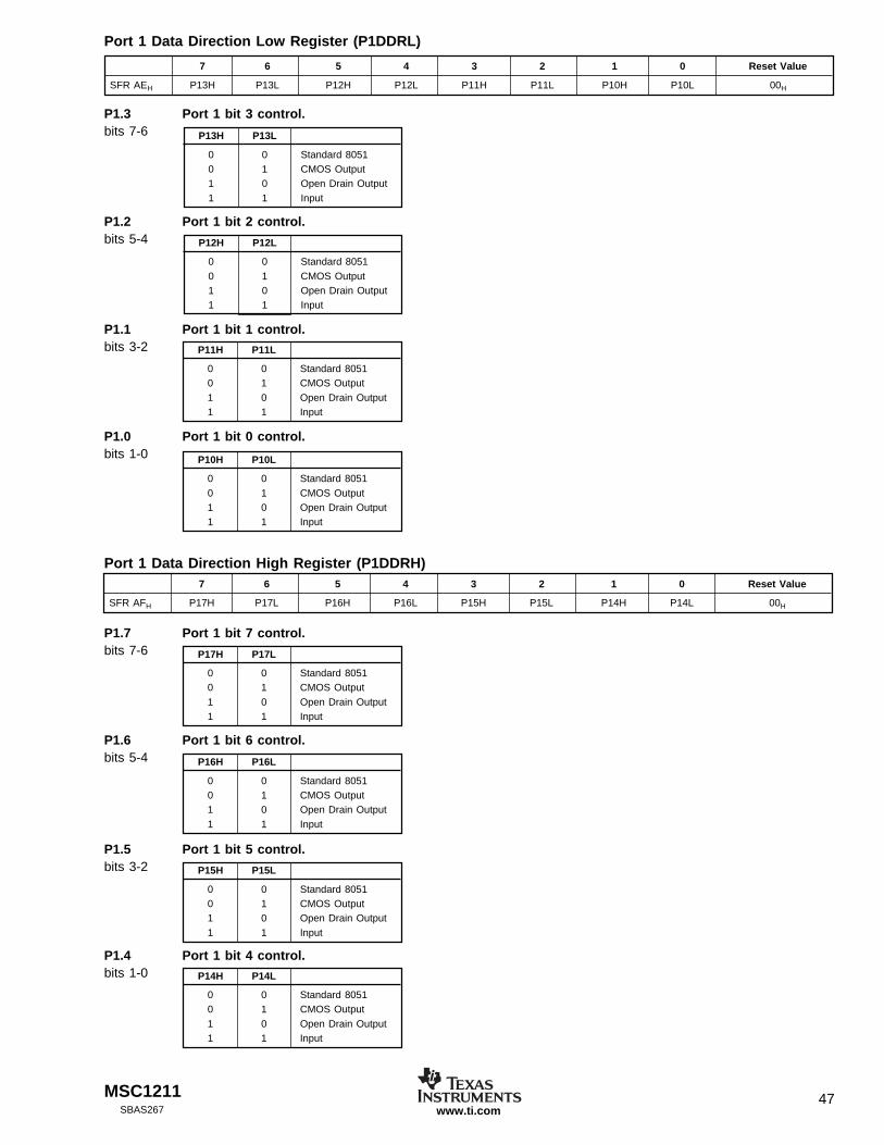
MSC1211 47SBAS267 www.ti.com
P1.1 Port 1 bit 1 control.bits 3-2
Port 1 Data Direction High Register (P1DDRH)
P1.0 Port 1 bit 0 control.bits 1-0
P11H P11L
0 0 Standard 80510 1 CMOS Output1 0 Open Drain Output1 1 Input
P10H P10L
0 0 Standard 80510 1 CMOS Output1 0 Open Drain Output1 1 Input
P1.7 Port 1 bit 7 control.bits 7-6
7 6 5 4 3 2 1 0 Reset Value
SFR AFH P17H P17L P16H P16L P15H P15L P14H P14L 00H
P17H P17L
0 0 Standard 80510 1 CMOS Output1 0 Open Drain Output1 1 Input
P1.6 Port 1 bit 6 control.bits 5-4 P16H P16L
0 0 Standard 80510 1 CMOS Output1 0 Open Drain Output1 1 Input
P1.5 Port 1 bit 5 control.bits 3-2 P15H P15L
0 0 Standard 80510 1 CMOS Output1 0 Open Drain Output1 1 Input
P1.4 Port 1 bit 4 control.bits 1-0 P14H P14L
0 0 Standard 80510 1 CMOS Output1 0 Open Drain Output1 1 Input
Port 1 Data Direction Low Register (P1DDRL)
P1.3 Port 1 bit 3 control.bits 7-6
7 6 5 4 3 2 1 0 Reset Value
SFR AEH P13H P13L P12H P12L P11H P11L P10H P10L 00H
P13H P13L
0 0 Standard 80510 1 CMOS Output1 0 Open Drain Output1 1 Input
P1.2 Port 1 bit 2 control.bits 5-4 P12H P12L
0 0 Standard 80510 1 CMOS Output1 0 Open Drain Output1 1 Input
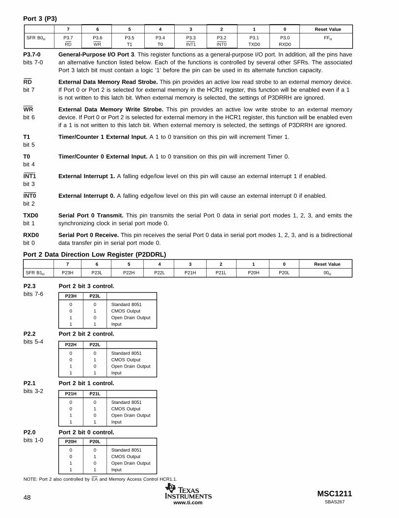
MSC121148SBAS267www.ti.com
Port 3 (P3)
P3.7-0 General-Purpose I/O Port 3. This register functions as a general-purpose I/O port. In addition, all the pins havebits 7-0 an alternative function listed below. Each of the functions is controlled by several other SFRs. The associated
Port 3 latch bit must contain a logic ‘1’ before the pin can be used in its alternate function capacity.
RD External Data Memory Read Strobe. This pin provides an active low read strobe to an external memory device.bit 7 If Port 0 or Port 2 is selected for external memory in the HCR1 register, this function will be enabled even if a 1
is not written to this latch bit. When external memory is selected, the settings of P3DRRH are ignored.
WR External Data Memory Write Strobe. This pin provides an active low write strobe to an external memorybit 6 device. If Port 0 or Port 2 is selected for external memory in the HCR1 register, this function will be enabled even
if a 1 is not written to this latch bit. When external memory is selected, the settings of P3DRRH are ignored.
T1 Timer/Counter 1 External Input. A 1 to 0 transition on this pin will increment Timer 1.bit 5
T0 Timer/Counter 0 External Input. A 1 to 0 transition on this pin will increment Timer 0.bit 4
INT1 External Interrupt 1. A falling edge/low level on this pin will cause an external interrupt 1 if enabled.bit 3
INT0 External Interrupt 0. A falling edge/low level on this pin will cause an external interrupt 0 if enabled.bit 2
TXD0 Serial Port 0 Transmit. This pin transmits the serial Port 0 data in serial port modes 1, 2, 3, and emits thebit 1 synchronizing clock in serial port mode 0.
RXD0 Serial Port 0 Receive. This pin receives the serial Port 0 data in serial port modes 1, 2, 3, and is a bidirectionalbit 0 data transfer pin in serial port mode 0.
Port 2 Data Direction Low Register (P2DDRL)
P2.3 Port 2 bit 3 control.bits 7-6
P2.2 Port 2 bit 2 control.bits 5-4
P2.1 Port 2 bit 1 control.bits 3-2
P2.0 Port 2 bit 0 control.bits 1-0
NOTE: Port 2 also controlled by EA and Memory Access Control HCR1.1.
7 6 5 4 3 2 1 0 Reset Value
SFR B0H P3.7 P3.6 P3.5 P3.4 P3.3 P3.2 P3.1 P3.0 FFH
RD WR T1 T0 INT1 INT0 TXD0 RXD0
7 6 5 4 3 2 1 0 Reset Value
SFR B1H P23H P23L P22H P22L P21H P21L P20H P20L 00H
P23H P23L
0 0 Standard 80510 1 CMOS Output1 0 Open Drain Output1 1 Input
P22H P22L
0 0 Standard 80510 1 CMOS Output1 0 Open Drain Output1 1 Input
P21H P21L
0 0 Standard 80510 1 CMOS Output1 0 Open Drain Output1 1 Input
P20H P20L
0 0 Standard 80510 1 CMOS Output1 0 Open Drain Output1 1 Input

MSC1211 49SBAS267 www.ti.com
Port 2 Data Direction High Register (P2DDRH)
P2.7 Port 2 bit 7 control.bits 7-6
7 6 5 4 3 2 1 0 Reset Value
SFR B2H P27H P27L P26H P26L P25H P25L P24H P24L 00H
P2.4 Port 2 bit 4 control.bits 1-0
P2.6 Port 2 bit 6 control.bits 5-4
P2.5 Port 2 bit 5 control.bits 3-2
Port 3 Data Direction Low Register (P3DDRL)
P27H P27L
0 0 Standard 80510 1 CMOS Output1 0 Open Drain Output1 1 Input
P26H P26L
0 0 Standard 80510 1 CMOS Output1 0 Open Drain Output1 1 Input
P25H P25L
0 0 Standard 80510 1 CMOS Output1 0 Open Drain Output1 1 Input
P24H P24L
0 0 Standard 80510 1 CMOS Output1 0 Open Drain Output1 1 Input
P3.3 Port 3 bit 3 control.bits 7-6
7 6 5 4 3 2 1 0 Reset Value
SFR B3H P33H P33L P32H P32L P31H P31L P30H P30L 00H
P3.2 Port 3 bit 2 control.bits 5-4
P3.1 Port 3 bit 1 control.bits 3-2
P3.0 Port 3 bit 0 control.bits 1-0
P33H P33L
0 0 Standard 80510 1 CMOS Output1 0 Open Drain Output1 1 Input
P32H P32L
0 0 Standard 80510 1 CMOS Output1 0 Open Drain Output1 1 Input
P31H P31L
0 0 Standard 80510 1 CMOS Output1 0 Open Drain Output1 1 Input
P30H P30L
0 0 Standard 80510 1 CMOS Output1 0 Open Drain Output1 1 Input
NOTE: Port 2 also controlled by EA and Memory Access Control HCR1.1.
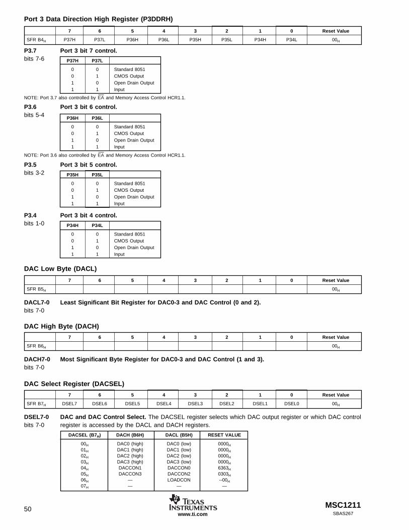
MSC121150SBAS267www.ti.com
Port 3 Data Direction High Register (P3DDRH)
7 6 5 4 3 2 1 0 Reset Value
SFR B4H P37H P37L P36H P36L P35H P35L P34H P34L 00H
P3.7 Port 3 bit 7 control.bits 7-6
P3.6 Port 3 bit 6 control.bits 5-4
P3.5 Port 3 bit 5 control.bits 3-2
P3.4 Port 3 bit 4 control.bits 1-0
P36H P36L
0 0 Standard 80510 1 CMOS Output1 0 Open Drain Output1 1 Input
P35H P35L
0 0 Standard 80510 1 CMOS Output1 0 Open Drain Output1 1 Input
P34H P34L
0 0 Standard 80510 1 CMOS Output1 0 Open Drain Output1 1 Input
P37H P37L
0 0 Standard 80510 1 CMOS Output1 0 Open Drain Output1 1 Input
7 6 5 4 3 2 1 0 Reset Value
SFR B5H 00H
NOTE: Port 3.7 also controlled by EA and Memory Access Control HCR1.1.
NOTE: Port 3.6 also controlled by EA and Memory Access Control HCR1.1.
DAC Low Byte (DACL)
DACL7-0 Least Significant Bit Register for DAC0-3 and DAC Control (0 and 2).bits 7-0
DAC High Byte (DACH)
7 6 5 4 3 2 1 0 Reset Value
SFR B6H 00H
DACH7-0 Most Significant Byte Register for DAC0-3 and DAC Control (1 and 3).bits 7-0
DSEL7-0 DAC and DAC Control Select. The DACSEL register selects which DAC output register or which DAC controlbits 7-0 register is accessed by the DACL and DACH registers.
7 6 5 4 3 2 1 0 Reset Value
SFR B7H DSEL7 DSEL6 DSEL5 DSEL4 DSEL3 DSEL2 DSEL1 DSEL0 00H
DACSEL (B7H) DACH (B6H) DACL (B5H) RESET VALUE
00H DAC0 (high) DAC0 (low) 0000H
01H DAC1 (high) DAC1 (low) 0000H
02H DAC2 (high) DAC2 (low) 0000H
03H DAC3 (high) DAC3 (low) 0000H
04H DACCON1 DACCON0 6363H
05H DACCON3 DACCON2 0303H
06H — LOADCON --00H
07H — — —
DAC Select Register (DACSEL)

MSC1211 51SBAS267 www.ti.com
DACSEL = 04H 7 6 5 4 3 2 1 0 Reset Value
SFR B5H COR0 EOD0 IDAC0DIS 0 0 SELREF0 DOM0_1 DOM0_0 63H
DAC0 Control Register (DACCON0)
COR0 Current Over Range on DAC0bit 7 Write: 0 = Clear to release from high-impedance state back to normal mode unless an over-range exists.
1 = NOP
Read: 0 = No current over range for DAC0.1 = COR0 signal after 3ms filter (EOD0 = 1) or raw signal (EOD0 = 0).
EOD0 Enable Over-Current Detectionbit 6 0 = Disable over-current detection.
1 = Enable over-current detection (default).
IDAC0DIS IDAC0 Disable (for DOM0 = 00)bit 5 0 = IDAC on mode for DAC0.
1 = IDAC off mode for DAC0 (default).
Not Usedbits 4-3
SELREF0 Select the Reference Voltage for DAC0 Voltage Reference.bit 2 0 = DAC0 VREF = AVDD (default).
1 = DAC0 VREF = internal VREF.
DOM0_1-0 DAC Output Mode DAC0.bits 1-0 DOM0 OUTPUT MODE FOR DAC0
00 Normal VDAC output, IDAC controlled by IDAC0DIS bit.01 Power-Down mode—VDAC output off 1kΩ to AGND, IDAC off.10 Power-Down mode—VDAC output off 100kΩ to AGND, IDAC off.11 Power-Down mode—VDAC output off high impedance, IDAC off (default).
DAC1 Control Register (DACCON1)
DACSEL = 04H 7 6 5 4 3 2 1 0 Reset Value
SFR B6H COR1 EOD1 IDAC1DIS 0 0 SELREF1 DOM1_1 DOM1_0 63H
COR1 Current Over Range on DAC1bit 7 Write: 0 = Clear to release from high-impedance state back to normal mode unless an over-range exists.
1 = NOP
Read: 0 = No current over range for DAC1.1 = COR1 signal after 3ms filter (EOD1 = 1) or raw signal (EOD1 = 0).
EOD1 Enable Over-Current Detectionbit 6 0 = Disable over-current detection.
1 = Enable over-current detection (default).
IDAC1DIS IDAC1 Disable (for DOM1 = 00)bit 5 0 = IDAC on mode for DAC1.
1 = IDAC off mode for DAC1 (default).
Not Usedbits 4-3
SELREF1 Select the Reference Voltage for DAC1 Voltage Reference.bit 2 0 = DAC1 VREF = AVDD (default).
1 = DAC1 VREF = internal VREF.
DOM1_1-0 DAC Output Mode DAC0.bits 1-0 DOM1 OUTPUT MODE FOR DAC1
00 Normal VDAC output, IDAC controlled by IDAC1DIS bit.01 Power-Down mode—VDAC output off 1kΩ to AGND, IDAC off.10 Power-Down mode—VDAC output off 100kΩ to AGND, IDAC off.11 Power-Down mode—VDAC output off high impedance, IDAC off (default).

MSC121152SBAS267www.ti.com
DAC2 Control Register (DACCON2)
DACSEL = 05H 7 6 5 4 3 2 1 0 Reset Value
SFR B5H 0 0 0 0 0 SELREF2 DOM2_1 DOM2_0 03H
SELREF2 Select the Reference Voltage for DAC2 Voltage Reference.bit 2 0 = DAC2 VREF = AVDD (default).
1 = DAC2 VREF = internal VREF.
DOM2_1-0 DAC Output Mode DAC2.bits 1-0 DOM2 OUTPUT MODE FOR DAC2
00 Normal VDAC output.01 Power-Down mode—VDAC output off 1kΩ to AGND, IDAC off.10 Power-Down mode—VDAC output off 100kΩ to AGND, IDAC off.11 Power-Down mode—VDAC output off high impedance, IDAC off (default).
DAC3 Control Register (DACCON3)
DACSEL = 05H 7 6 5 4 3 2 1 0 Reset Value
SFR B6H 0 0 0 0 0 SELREF3 DOM3_1 DOM3_0 03H
SELREF3 Select the Reference Voltage for DAC3 Voltage Reference.bit 2 0 = DAC2 VREF = AVDD (default).
1 = DAC2 VREF = internal VREF.
DOM3_1-0 DAC Output Mode DAC3.bits 1-0 DOM2 OUTPUT MODE FOR DAC2
00 Normal VDAC output.01 Power-Down mode—VDAC output off 1kΩ to AGND, IDAC off.10 Power-Down mode—VDAC output off 100kΩ to AGND, IDAC off.11 Power-Down mode—VDAC output off high impedance, IDAC off (default).
DAC Load Control Register (LOADCON)
DACSEL = 06H 7 6 5 4 3 2 1 0 Reset Value
SFR B5H D3LOAD1 D3LOAD0 D2LOAD1 D2LOAD0 D1LOAD1 D1LOAD0 D0LOAD1 D0LOAD0 00H
D3LOAD1-0 DAC Load Options.bit 7-6
D2LOAD1-0bit 5-4
D1LOAD1-0bit 3-2
D0LOAD1-0bit 1-0
DxLOAD OUTPUT MODE FOR DACx
00 Direct load: write to DACxL directly loads the DAC buffer and the DAC output (write to DACxH does not load DAC output).01 Delay load: the values last written to DACxL/DACxH will be transferred to the DAC output on the next MSEC timer tick.10 Delay load: the values last written to DACxL/DACxH will be transferred to the DAC output on the next HMSEC timer tick.11 Sync load: the values contained in the DACxL/DACxH registers will be transferred to the DAC output immediately after
11B is written to this register.

MSC1211 53SBAS267 www.ti.com
SM0-2 Serial Port 1 Mode. These bits control the mode of serial Port 1. Modes 1, 2, and 3 have 1 start and 1 stop bitbits 7-5 in addition to the 8 or 9 data bits.
7 6 5 4 3 2 1 0 Reset Value
SFR C0H SM0_1 SM1_1 SM2_1 REN_1 TB8_1 RB8_1 TI_1 RI_1 00H
REN_1 Receive Enable. This bit enables/disables the serial Port 1 received shift register.bit 4 0 = Serial Port 1 reception disabled.
1 = Serial Port 1 received enabled (modes 1, 2, and 3). Initiate synchronous reception (mode 0).
TB8_1 9th Transmission Bit State. This bit defines the state of the 9th transmission bit in serial Port 1 modes 2 and 3.bit 3
RB8_1 9th Received Bit State. This bit identifies the state of the 9th reception bit of received data in serial Port 1 modesbit 2 2 and 3. In serial port mode 1, when SM2_1 = 0, RB8_1 is the state of the stop bit. RB8_1 is not used in mode 0.
TI_1 Transmitter Interrupt Flag. This bit indicates that data in the serial Port 1 buffer has been completely shiftedbit 1 out. In serial port mode 0, TI_1 is set at the end of the 8th data bit. In all other modes, this bit is set at the end
of the last data bit. This bit must be cleared by software to transmit the next byte.
MODE SM0 SM1 SM2 FUNCTION LENGTH PERIOD
0 0 0 0 Synchronous 8 bits 12 pCLK(1)
0 0 0 1 Synchronous 8 bits 4 pCLK(1)
1(2) 0 1 x Asynchronous 10 bits Timer 1 or 2 Baud Rate Equation
2 1 0 0 Asynchronous 11 bits 64 pCLK(1) (SMOD = 0)
32 pCLK(1) (SMOD = 1)
2 1 0 1 Asynchronous with 11 bits 64 pCLK(1) (SMOD = 0)
Multiprocessor Communication 32 pCLK(1) (SMOD = 1)
3(2) 1 1 0 Asynchronous 11 bits Timer 1 or 2 Baud Rate Equation3(2) 1 1 1 Asynchronous with 11 bits Timer 1 or 2 Baud Rate Equation
Multiprocessor Communication
NOTE: (1) pCLK will be equal to tCLK, except that pCLK will stop for IDLE. (2) For modes 1 and 3, the selection ofTimer 1 or 2 for baud rate is specified via the SCON register.
Interrupt Priority (IP)
PS1 Serial Port 1 Interrupt. This bit controls the priority of the serial Port 1 interrupt.bit 6 0 = Serial Port 1 priority is determined by the natural priority order.
1 = Serial Port 1 is a high priority interrupt.
PT2 Timer 2 Interrupt. This bit controls the priority of the Timer 2 interrupt.bit 5 0 = Timer 2 priority is determined by the natural priority order.
1 = Timer 2 priority is a high priority interrupt.
PS0 Serial Port 0 Interrupt. This bit controls the priority of the serial Port 0 interrupt.bit 4 0 = Serial Port 0 priority is determined by the natural priority order.
1 = Serial Port 0 is a high priority interrupt.
PT1 Timer 1 Interrupt. This bit controls the priority of the Timer 1 interrupt.bit 3 0 = Timer 1 priority is determined by the natural priority order.
1 = Timer 1 priority is a high priority interrupt.
PX1 External Interrupt 1. This bit controls the priority of external interrupt 1.bit 2 0 = External interrupt 1 priority is determined by the natural priority order.
1 = External interrupt 1 is a high priority interrupt.
PT0 Timer 0 Interrupt. This bit controls the priority of the Timer 0 interrupt.bit 1 0 = Timer 0 priority is determined by the natural priority order.
1 = Timer 0 priority is a high priority interrupt.
PX0 External Interrupt 0. This bit controls the priority of external interrupt 0.bit 0 0 = External interrupt 0 priority is determined by the natural priority order.
1 = External interrupt 0 is a high priority interrupt.
Serial Port 1 Control (SCON1)
7 6 5 4 3 2 1 0 Reset Value
SFR B8H 1 PS1 PT2 PS0 PT1 PX1 PT0 PX0 80H

MSC121154SBAS267www.ti.com
Auxialiary interrupts will wake up from IDLE. They are enabled with EAI (EICON.5).
EWUWDT Enable Wake Up Watchdog Timer. Wake using watchdog timer interrupt.bit 2 0 = Don’t wake up on watchdog timer interrupt.
1 = Wake up on watchdog timer interrupt.
EWUEX1 Enable Wake Up External 1. Wake using external interrupt source 1.bit 1 0 = Don’t wake up on external interrupt source 1.
1 = Wake up on external interrupt source 1.
EWUEX0 Enable Wake Up External 0. Wake using external interrupt source 0.bit 0 0 = Don’t wake up on external interrupt source 0.
1 = Wake up on external interrupt source 0.
System Clock Divider Register (SYSCLK)
RI_1 Receiver Interrupt Flag. This bit indicates that a byte of data has been received in the serial Port 1 buffer. Inbit 0 serial port mode 0, RI_1 is set at the end of the 8th bit. In serial port mode 1, RI_1 is set after the last sample
of the incoming stop bit subject to the state of SM2_1. In modes 2 and 3, RI_1 is set after the last sample ofRB8_1. This bit must be cleared by software to receive the next byte.
Serial Data Buffer 1 (SBUF1)
SBUF1.7-0 Serial Data Buffer 1. Data for serial Port 1 is read from or written to this location. The serial transmit and receivebits 7-0 buffers are separate registers, but both are addressed at this location.
Enable Wake Up (EWU) Waking Up from IDLE Mode
7 6 5 4 3 2 1 0 Reset Value
SFR C1H 00H
7 6 5 4 3 2 1 0 Reset Value
SFR C6H — — — — — EWUWDT EWUEX1 EWUEX0 00H
7 6 5 40 3 2 1 0 Reset Value
SFR C7H 0 0 DIVMOD1 DIVMOD0 0 DIV2 DIV1 DIV0 00H
DIVMOD DIVIDE MODE
00 Normal mode (default, no divide)
01 Immediate mode: start divide immediately, return to Normal mode on IDLE wakeup condition..
10 Delay mode: same as Immediate mode, except that the mode changes with the millisecond interrupt (MSINT). If MSINT isenabled, the divide will start on the next MSINT and return to normal mode on the following MSINT. If MSINT is notenabled, the divide will start on the next MSINT condition (even if masked) but will not leave the divide mode until theMSINT counter overflows, which follows a wakeup condition.
11 Reserved
DIVMOD DIVISION MODE STATUS
00 No divide01 Divider is in Immediate mode10 Divider is in Delay mode11 Reserved
DIV DIVISOR
000 Divide by 2 (default)001 Divide by 4010 Divide by 8011 Divide by 16100 Divide by 32101 Divide by 1024110 Divide by 2048111 Divide by 4096
DIVMOD1-0 Clock Divide Modebits 5-4 Write:
Read:
DIV2-0 Divide Modebit 2-0
NOTE:
Do not clear the DIVMOD register to exit Immediateor Delay modes. Exit these modes only through theappropriate interrupt (the interrupt can be eithernormally generated or software generated).

MSC1211 55SBAS267 www.ti.com
Timer 2 Control (T2CON)
TF2 Timer 2 Overflow Flag. This flag will be set when Timer 2 overflows from FFFFH. It must be cleared by software.bit 7 TF2 will only be set if RCLK and TCLK are both cleared to 0. Writing a 1 to TF2 forces a Timer 2 interrupt if enabled.
EXF2 Timer 2 External Flag. A negative transition on the T2EX pin (P1.1) will cause this flag to be set based onbit 6 the EXEN2 (T2CON.3) bit. If set by a negative transition, this flag must be cleared to 0 by software.
Setting this bit in software will force a timer interrupt if enabled.
RCLK Receive Clock Flag. This bit determines the serial Port 0 timebase when receiving data in serial modes 1 or 3.bit 5 0 = Timer 1 overflow is used to determine receiver baud rate for UART0.
1 = Timer 2 overflow is used to determine receiver baud rate for UART0.Setting this bit will force Timer 2 into baud rate generation mode. The timer will operate from a divide by 2 ofthe external clock.
TCLK Transmit Clock Flag. This bit determines the serial Port 0 timerbase when transmitting data in serial modes 1 or 3.bit 4 0 = Timer 1 overflow is used to determine transmitter baud rate for UART0.
1 = Timer 2 overflow is used to determine transmitter baud rate for UART0.Setting this bit will force Timer 2 into baud rate generation mode. The timer will operate from a divide by 2 ofthe external clock.
EXEN2 Timer 2 External Enable. This bit enables the capture/reload function on the T2EX pin if Timer 2 is notbit 3 generating baud rates for the serial port.
0 = Timer 2 will ignore all external events at T2EX.1 = Timer 2 will capture or reload a value if a negative transition is detected on the T2EX pin.
TR2 Timer 1 Run Control. This bit enables/disables the operation of Timer 2. Halting this timer will preserve thebit 2 current count in TH2, TL2.
0 = Timer 2 is halted.1 = Timer 2 is enabled.
C/T2 Counter/Timer Select. This bit determines whether Timer 2 will function as a timer or counter. Independent ofbit 1 this bit, Timer 2 runs at 2 clocks per tick when used in baud rate generator mode.
0 = Timer 2 functions as a timer. The speed of Timer 2 is determined by the T2M bit (CKCON.5).1 = Timer 2 will count negative transitions on the T2 pin (P1.0).
CP/RL2 Capture/Reload Select. This bit determines whether the capture or reload function will be used for Timer 2. Ifbit 0 either RCLK or TCLK is set, this bit will not function and the timer will function in an auto-reload mode
following each overflow.0 = Auto-reloads will occur when Timer 2 overflows or a falling edge is detected on T2EX if EXEN2 = 1.1 = Timer 2 captures will occur when a falling edge is detected on T2EX if EXEN2 = 1.
Timer 2 Capture LSB (RCAP2L)
7 6 5 4 3 2 1 0 Reset Value
SFR C8H TF2 EXF2 RCLK TCLK EXEN2 TR2 C/T2 CP/RL2 00H
RCAP2L Timer 2 Capture LSB. This register is used to capture the TL2 value when Timer 2 is configured in capturebits 7-0 mode. RCAP2L is also used as the LSB of a 16-bit reload value when Timer 2 is configured in auto-reload mode.
7 6 5 4 3 2 1 0 Reset Value
SFR CAH 00H

MSC121156SBAS267www.ti.com
Timer 2 Capture MSB (RCAP2H)
TL2 Timer 2 LSB. This register contains the least significant byte of Timer 2.bits 7-0
Timer 2 MSB (TH2)
7 6 5 4 3 2 1 0 Reset Value
SFR CBH 00H
RCAP2H Timer 2 Capture MSB. This register is used to capture the TH2 value when Timer 2 is configured in capturebits 7-0 mode. RCAP2H is also used as the MSB of a 16-bit reload value when Timer 2 is configured in auto-reload
mode.
Timer 2 LSB (TL2)
7 6 5 4 3 2 1 0 Reset Value
SFR CCH 00H
TH2 Timer 2 MSB. This register contains the most significant byte of Timer 2.bits 7-0
Program Status Word (PSW)
7 6 5 4 3 2 1 0 Reset Value
SFR CDH 00H
CY Carry Flag. This bit is set when the last arithmetic operation resulted in a carry (during addition) or a borrowbit 7 (during subtraction). Otherwise it is cleared to 0 by all arithmetic operations.
AC Auxiliary Carry Flag. This bit is set to 1 if the last arithmetic operation resulted in a carry into (during addition),bit 6 or a borrow (during substraction) from the high order nibble. Otherwise it is cleared to 0 by all arithmetic
operations.
F0 User Flag 0. This is a bit-adressable, general-purpose flag for software control.bit 5
RS1, RS0 Register Bank Select 1-0. These bits select which register bank is addressed during register accesses.bits 4-3
OV Overflow Flag. This bit is set to 1 if the last arithmetic operation resulted in a carry (addition), borrowbit 2 (subtraction), or overflow (multiply or divide). Otherwise it is cleared to 0 by all arithmetic operations.
F1 User Flag 1. This is a bit-addressable, general-purpose flag for software control.bit 1
P Parity Flag. This bit is set to 1 if the modulo-2 sum of the 8 bits of the accumulator is 1 (odd parity); andbit 0 cleared to 0 on even parity.
ADC Offset Calibration Register Low Byte (OCL)
7 6 5 4 3 2 1 0 Reset Value
SFR D0H CY AC F0 RS1 RS0 OV F1 P 00H
RS1 RS0 REGISTER BANK ADDRESS
0 0 0 00H-07H
0 1 1 08H-0FH
1 0 2 10H-17H
1 1 3 18H-1FH
OCL ADC Offset Calibration Register Low Byte. This is the low byte of the 24-bit word that contains thebits 7-0 ADC offset calibration. A value which is written to this location will set the ADC offset calibration value.
7 6 5 4 3 2 1 0 Reset Value
SFR D1H 00H

MSC1211 57SBAS267 www.ti.com
GCL ADC Gain Calibration Register Low Byte. This is the low byte of the 24-bit word that contains the ADCbits 7-0 gain calibration. A value which is written to this location will set the ADC gain calibration value.
ADC Gain Calibration Register Middle Byte (GCM)
ADC Offset Calibration Register Middle Byte (OCM)
7 6 5 4 3 2 1 0 Reset Value
SFR D2H 00H
OCM ADC Offset Calibration Register Middle Byte. This is the middle byte of the 24-bit word that contains the ADCbits 7-0 offset calibration. A value which is written to this location will set the ADC offset calibration value.
ADC Offset Calibration Register High Byte (OCH)
7 6 5 4 3 2 1 0 Reset Value
SFR D3H 00H
OCH ADC Offset Calibration Register High Byte. This is the high byte of the 24-bit word that contains thebits 7-0 ADC offset calibration. A value which is written to this location will set the ADC offset calibration value.
ADC Gain Calibration Register Low Byte (GCL)
7 6 5 4 3 2 1 0 Reset Value
SFR D4H 5AH
GCM ADC Gain Calibration Register Middle Byte. This is the middle byte of the 24-bit word that containsbits 7-0 the ADC gain calibration. A value which is written to this location will set the ADC gain calibration value.
ADC Gain Calibration Register High Byte (GCH)
7 6 5 4 3 2 1 0 Reset Value
SFR D5H ECH
GCH ADC Gain Calibration Register High Byte. This is the high byte of the 24-bit word that contains thebits 7-0 ADC gain calibration. A value which is written to this location will set the ADC gain calibration value.
ADC Multiplexer Register (ADMUX)
7 6 5 4 3 2 1 0 Reset Value
SFR D6H 5FH
INP3-0 Input Multiplexer Positive Channel. This selects the positive signal input.bits 7-4
7 6 5 4 3 2 1 0 Reset Value
SFR D7H INP3 INP2 INP1 INP0 INN3 INN2 INN1 INN0 01H
INP3 INP2 INP1 INP0 POSITIVE INPUT
0 0 0 0 AIN0 (default)0 0 0 1 AIN10 0 1 0 AIN20 0 1 1 AIN30 1 0 0 AIN40 1 0 1 AIN50 1 1 0 AIN60 1 1 1 AIN71 0 0 0 AINCOM1 1 1 1 Temperature Sensor (Requires ADMUX = FFH)
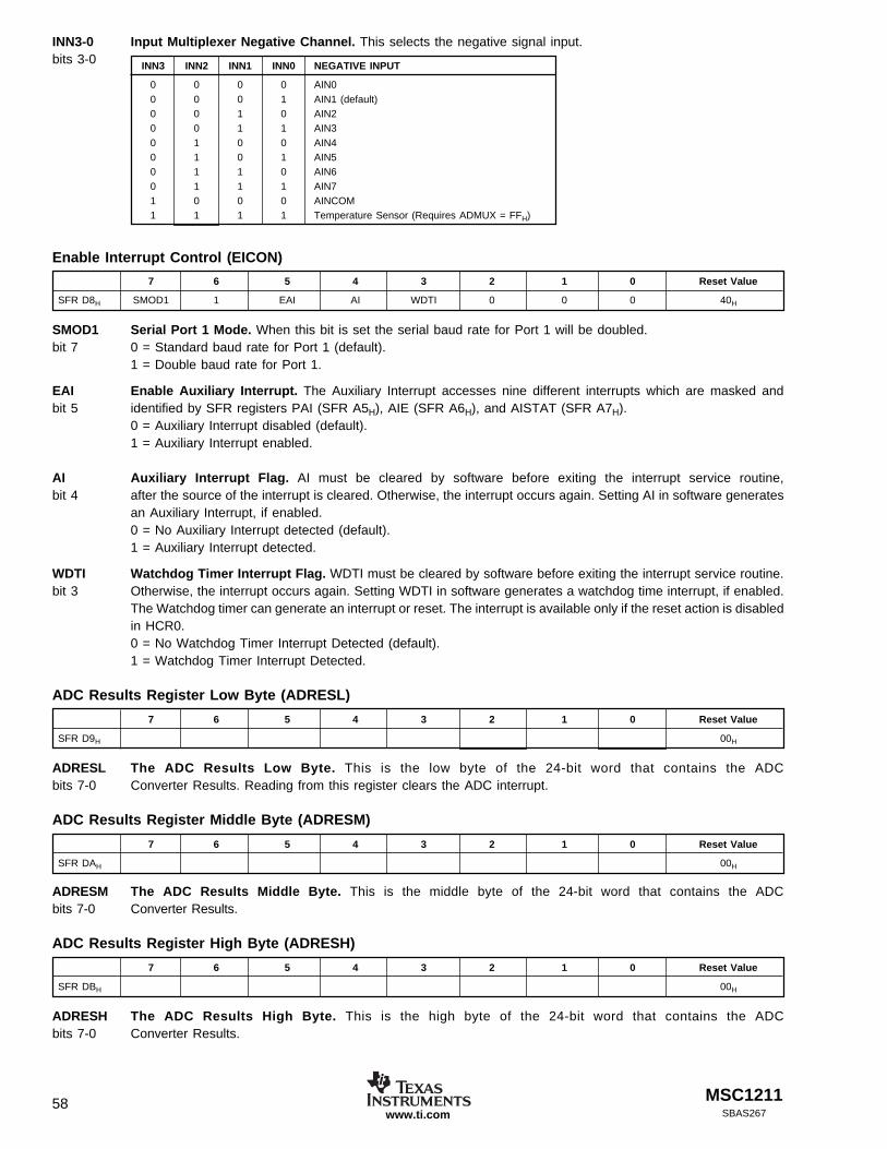
MSC121158SBAS267www.ti.com
INN3-0 Input Multiplexer Negative Channel. This selects the negative signal input.bits 3-0 INN3 INN2 INN1 INN0 NEGATIVE INPUT
0 0 0 0 AIN00 0 0 1 AIN1 (default)0 0 1 0 AIN20 0 1 1 AIN30 1 0 0 AIN40 1 0 1 AIN50 1 1 0 AIN60 1 1 1 AIN71 0 0 0 AINCOM1 1 1 1 Temperature Sensor (Requires ADMUX = FFH)
7 6 5 4 3 2 1 0 Reset Value
SFR D8H SMOD1 1 EAI AI WDTI 0 0 0 40H
Enable Interrupt Control (EICON)
ADRESL The ADC Results Low Byte. This is the low byte of the 24-bit word that contains the ADCbits 7-0 Converter Results. Reading from this register clears the ADC interrupt.
ADC Results Register Middle Byte (ADRESM)
SMOD1 Serial Port 1 Mode. When this bit is set the serial baud rate for Port 1 will be doubled.bit 7 0 = Standard baud rate for Port 1 (default).
1 = Double baud rate for Port 1.
EAI Enable Auxiliary Interrupt. The Auxiliary Interrupt accesses nine different interrupts which are masked andbit 5 identified by SFR registers PAI (SFR A5H), AIE (SFR A6H), and AISTAT (SFR A7H).
0 = Auxiliary Interrupt disabled (default).1 = Auxiliary Interrupt enabled.
AI Auxiliary Interrupt Flag. AI must be cleared by software before exiting the interrupt service routine,bit 4 after the source of the interrupt is cleared. Otherwise, the interrupt occurs again. Setting AI in software generates
an Auxiliary Interrupt, if enabled.0 = No Auxiliary Interrupt detected (default).1 = Auxiliary Interrupt detected.
WDTI Watchdog Timer Interrupt Flag. WDTI must be cleared by software before exiting the interrupt service routine.bit 3 Otherwise, the interrupt occurs again. Setting WDTI in software generates a watchdog time interrupt, if enabled.
The Watchdog timer can generate an interrupt or reset. The interrupt is available only if the reset action is disabledin HCR0.0 = No Watchdog Timer Interrupt Detected (default).1 = Watchdog Timer Interrupt Detected.
ADC Results Register Low Byte (ADRESL)
7 6 5 4 3 2 1 0 Reset Value
SFR D9H 00H
7 6 5 4 3 2 1 0 Reset Value
SFR DAH 00H
ADRESM The ADC Results Middle Byte. This is the middle byte of the 24-bit word that contains the ADCbits 7-0 Converter Results.
ADC Results Register High Byte (ADRESH)
ADRESH The ADC Results High Byte. This is the high byte of the 24-bit word that contains the ADCbits 7-0 Converter Results.
7 6 5 4 3 2 1 0 Reset Value
SFR DBH 00H

MSC1211 59SBAS267 www.ti.com
ADC Control Register 0 (ADCON0)
7 6 5 4 3 2 1 0 Reset Value
SFR DCH — BOD EVREF VREFH EBUF PGA2 PGA1 PGA0 30H
BOD Burnout Detect. When enabled this connects a positive current source to the positive channel and a negativebit 6 current source to the negative channel. If the channel is open circuit then the ADC results will be full-scale.
0 = Burnout Current Sources Off (default).1 = Burnout Current Sources On.
EVREF Enable Internal Voltage Reference. If the internal voltage reference is not used, it should be turned off to savebit 5 power and reduce noise.
0 = Internal Voltage Reference Off.1 = Internal Voltage Reference On (default).
VREFH Voltage Reference High Select. The internal voltage reference can be selected to be 2.5V or 1.25V.bit 4 0 = REFOUT/REF IN+ is 1.25V.
1 = REFOUT/REF IN+ is 2.5V (default).
EBUF Enable Buffer. Enable the input buffer to provide higher input impedance but limits the input voltage range andbit 3 dissipates more power.
0 = Buffer disabled (default).1 = Buffer enabled.
PGA2-0 Programmable Gain Amplifier. Sets the gain for the PGA from 1 to 128.bits 2-0 PGA2 PGA1 PGA0 GAIN
0 0 0 1 (default)0 0 1 20 1 0 40 1 1 81 0 0 161 0 1 321 1 0 641 1 1 128
ADC Control Register 1 (ADCON1)
POL Polarity. Polarity of the ADC result and Summation register.bit 6 0 = Bipolar.
1 = Unipolar.
7 6 5 4 3 2 1 0 Reset Value
SFR DDH — POL SM1 SM0 — CAL2 CAL1 CAL0 x000 0000B
POL ANALOG INPUT DIGITAL OUTPUT
+FSR 0x7FFFFF0 ZERO 0x000000
–FSR 0x800000
+FSR 0xFFFFFF1 ZERO 0x000000
–FSR 0x000000
SM1 SM0 SETTLING MODE
0 0 Auto0 1 Fast Settling Filter1 0 Sinc2 Filter1 1 Sinc3 Filter
SM1-0 Settling Mode. Selects the type of filter or auto select which defines the digital filter settling characteristics.bits 5-4

MSC121160SBAS267www.ti.com
CAL2-0 Calibration Mode Control Bits.bits 2-0
ADC Control Register 2 (ADCON2)
CAL2 CAL1 CAL0 CALIBRATION MODE
0 0 0 No Calibration (default)0 0 1 Self Calibration, Offset and Gain0 1 0 Self Calibration, Offset Only0 1 1 Self Calibration, Gain Only1 0 0 System Calibration, Offset Only1 0 1 System Calibration, Gain Only1 1 0 Reserved1 1 1 Reserved
DR7-0 Decimation Ratio LSB.bits 7-0
ADC Control Register 3 (ADCON3)
7 6 5 4 3 2 1 0 Reset Value
SFR DEH DR7 DR6 DR5 DR4 DR3 DR2 DR1 DR0 1BH
DR10-8 Decimation Ratio Most Significant 3 Bits. The output data rate = (ACLK + 1)/64/Decimation Ratio.bits 2-0
Accumulator (A or ACC)
7 6 5 4 3 2 1 0 Reset Value
SFR E0H ACC.7 ACC.6 ACC.5 ACC.4 ACC.3 ACC.2 ACC.1 ACC.0 00H
ACC.7-0 Accumulator. This register serves as the accumulator for arithmetic and logic operations.bits 7-0
Summation/Shifter Control (SSCON)
The Summation register is powered down when the ADC is powered down. If all zeroes are written to this register the 32-bitSUMR3-0 registers will be cleared. The Summation registers will do sign extend if Bipolar is selected in ADCON1.
SSCON1-0 Summation/Shift Control.bits 7-6
7 6 5 4 3 2 1 0 Reset Value
SFR E1H SSCON1 SSCON0 SCNT2 SCNT1 SCNT0 SHF2 SHF1 SHF0 00H
SCNT2-0 Summation Count. When the summation is complete an interrupt will be generated unless masked. Reading thebits 5-3 SUMR0 register clears the interrupt.
SCNT2 SCNT1 SCNT0 SUMMATION COUNT
0 0 0 20 0 1 40 1 0 80 1 1 161 0 0 321 0 1 641 1 0 1281 1 1 256
Read Value—000B.
7 6 5 4 3 2 1 0 Reset Value
SFR DFH — — — — — DR10 DR9 DR8 06H
SSCON1 SSCON0 SCNT2 SCNT1 SCNT0 SHF2 SHF1 SHF0 DESCRIPTION
0 0 0 0 0 0 0 0 Clear Summation Register0 0 0 1 0 0 0 0 CPU Summation on Write to SUMR00 0 1 0 0 0 0 0 CPU Subtraction on Write to SUMR01 0 x x x Note (1) Note (1) Note (1) CPU Shift Only0 1 Note (1) Note (1) Note (1) x x x ADC Summation Only1 1 Note (1) Note (1) Note (1) Note (1) Note (1) Note (1) ADC Summation Completes then Shift Completes
NOTES: (1) Refer to register bit definition.

MSC1211 61SBAS267 www.ti.com
SHF2-0 Shift Count.bits 2-0
Summation Register 0 (SUMR0)
SUMR0 Summation Register 0. This is the least significant byte of the 32-bit summation register or bits 0 to 7.bits 7-0 Write: will cause values in SUMR3-0 to be added to the summation register.
Read: will clear the Summation Count Interrupt.
Summation Register 1 (SUMR1)
SHF2 SHF1 SHF0 SHIFT DIVIDE
0 0 0 1 20 0 1 2 40 1 0 3 80 1 1 4 161 0 0 5 321 0 1 6 641 1 0 7 1281 1 1 8 256
7 6 5 4 3 2 1 0 Reset Value
SFR E2H 00H
SUMR1 Summation Register 1. This is the most significant byte of the lowest 16 bits of the summation register or bits 8-15.bits 7-0
Summation Register 2 (SUMR2)
7 6 5 4 3 2 1 0 Reset Value
SFR E3H 00H
SUMR2 Summation Register 2. This is the most significant byte of the lowest 24 bits of the summation register or bits 16-23.bits 7-0
Summation Register 3 (SUMR3)
7 6 5 4 3 2 1 0 Reset Value
SFR E4H 00H
7 6 5 4 3 2 1 0 Reset Value
SFR E5H 00H
SUMR3 Summation Register 3. This is the most significant byte of the 32-bit summation register or bits 24-31.bits 7-0
Offset DAC Register (ODAC)
ODAC Offset DAC Register. This register will shift the input by up to half of the ADC input range. The leastbits 7-0 significant bit is equal to the input voltage range divided by 256. The input range will depend on the setting
of the PGA. The ODAC is a signed magnitude register with bit 7 providing the sign of the offset and bits 6-0providing the magnitude.
bit 7 Offset DAC Sign bit.0 = Positive1 = Negative
bit 6-0 Offset = V
PGAODACREF bit
26 0
1271 7
••
• −[ : ]( )
NOTE: The offset must be used after calibration or the calibration will nullify the effects.
7 6 5 4 3 2 1 0 Reset Value
SFR E6H 00H

MSC121162SBAS267www.ti.com
Low Voltage Detect Control (LVDCON)
ALVDIS Analog Low Voltage Detect Disable.bit 7 0 = Enable Detection of Low Analog Supply Voltage.
1 = Disable Detection of Low Analog Supply Voltage.
ALVD2-0 Analog Voltage Detection Level.bits 6-4
7 6 5 4 3 2 1 0 Reset Value
SFR E7H ALVDIS ALVD2 ALVD1 ALVD0 DLVDIS DLVD2 DLVD1 DLVD0 00H
DLVDIS Digital Low Voltage Detect Disable.bit 3 0 = Enable Detection of Low Digital Supply Voltage.
1 = Disable Detection of Low Digital Supply Voltage.
DLVD2-0 Digital Voltage Detection Level.bits 2-0
Extended Interrupt Enable (EIE)
7 6 5 4 3 2 1 0 Reset Value
SFR E8H 1 1 1 EWDI EX5 EX4 EX3 EX2 E0H
EWDI Enable Watchdog Interrupt. This bit enables/disables the watchdog interrupt. The Watchdog timer is enabled bythe WDTCON (SFR FFH) and PDCON (SFR F1H) registers.
bit 4 0 = Disable the Watchdog Interrupt1 = Enable Interrupt Request Generated by the Watchdog Timer
EX5 External Interrupt 5 Enable. This bit enables/disables external interrupt 5.bit 3 0 = Disable External Interrupt 5
1 = Enable External Interrupt 5
EX4 External Interrupt 4 Enable. This bit enables/disables external interrupt 4.bit 2 0 = Disable External Interrupt 4
1 = Enable External Interrupt 4
EX3 External Interrupt 3 Enable. This bit enables/disables external interrupt 3.bit 1 0 = Disable External Interrupt 3
1 = Enable External Interrupt 3
EX2 External Interrupt 2 Enable. This bit enables/disables external interrupt 2.bit 0 0 = Disable External Interrupt 2
1 = Enable External Interrupt 2
ALVD2 ALVD1 ALVD0 VOLTAGE LEVEL
0 0 0 AVDD 2.7V (default)0 0 1 AVDD 3.0V0 1 0 AVDD 3.3V0 1 1 AVDD 4.0V1 0 0 AVDD 4.2V1 0 1 AVDD 4.5V1 1 0 AVDD 4.7V1 1 1 External Voltage AIN7 Compared to 1.2V
DLVD2 DLVD1 DLVD0 VOLTAGE LEVEL
0 0 0 DVDD 2.7V (default)0 0 1 DVDD 3.0V0 1 0 DVDD 3.3V0 1 1 DVDD 4.0V1 0 0 DVDD 4.2V1 0 1 DVDD 4.5V1 1 0 DVDD 4.7V1 1 1 External Voltage AIN6 Compared to 1.2V

MSC1211 63SBAS267 www.ti.com
Hardware Product Code Register 0 (HWPC0)
HWPC0.7-0 Hardware Product Code LSB. Read only.bits 7-0
7 6 5 4 3 2 1 0 Reset Value
SFR E9H HWPC0.7 HWPC0.6 HWPC0.5 HWPC0.4 HWPC0.3 1 MEMORY SIZE 0000_001xxB
7 6 5 4 3 2 1 0 Reset Value
SFR EAH 1 08H
HWPC1.7-0 Hardware Product Code MSB. Read only.bits 7-0
Hardware Version Register (HDWVER)
PGERA Page Erase. Available in both user and program modes.bit 6 0 = Disable Page Erase Mode
1 = Enable Page Erase Mode
FRCM Frequency Control Mode. The bypass is only used for slow clocks to save power.bit 4 0 = Bypass (default)
1 = Use Delay Line. Saves power (Recommended).
BUSY Write/Erase BUSY Signal.bit 2 0 = Idle or Available
1 = Busy
Flash Memory Timing Control Register (FTCON)
7 6 5 4 3 2 1 0 Reset Value
SFR EEH 0 PGERA 0 FRCM 0 BUSY 1 0 02H
7 6 5 4 3 2 1 0 Reset Value
SFR EFH FER3 FER2 FER1 FER0 FWR3 FWR2 FWR1 FWR0 A5H
MEMORY SIZE MODEL FLASH MEMORY
0 0 MSC1211Y2 4kB0 1 MSC1211Y3 8kB1 0 MSC1211Y4 16kB1 1 MSC1211Y5 32kB
Hardware Product Code Register 1 (HWPC1)
Refer to Flash Timing Characteristics
FER3-0 Set Erase. Flash Erase Time = (1 + FER) • (MSEC + 1) • tCLK.bits 7-4 11ms industrial temperature range.
5ms commercial temperature range.
FWR3-0 Set Write. Flash Write Time = (1 + FWR) • (USEC + 1) • 5 • tCLK.bits 3-0 30µs to 40µs.
7 6 5 4 3 2 1 0 Reset Value
SFR EBH
Flash Memory Control (FMCON)

MSC121164SBAS267www.ti.com
B Register (B)
PSEN2-0 PSEN Mode Select.bits 5-3
B.7-0 B Register. This register serves as a second accumulator for certain arithmetic operations.bits 7-0
Power-Down Control Register (PDCON)
7 6 5 4 3 2 1 0 Reset Value
SFR F0H B.7 B.6 B.5 B.4 B.3 B.2 B.1 B.0 00H
7 6 5 4 3 2 1 0 Reset Value
SFR F1H 0 PDDAC PDI2C PDPWM PDAD PDWDT PDST PDSPI 7FH
Turning peripheral modules off puts the MSC1211 in the lowest power mode.
PDDAC Pulse Width Module Control.bit 6 0 = DACs On
1 = DACs Power Down
PDI2C I2C Control.bit 5 0 = I2C On (the state is undefined if PDSPI is also = 0)
1 = I2C Power Down
PDPWM Pulse Width Module Control.bit 4 0 = PWM On
1 = PWM Power Down
PDAD ADC Control.bit 3 0 = ADC On
1 = ADC, VREF, Summation registers, and Analog Brownout are powered down. Analog current = 0.
PDWDT Watchdog Timer Control.bit 2 0 = Watchdog Timer On
1 = Watchdog Timer Power Down
PDST System Timer Control.bit 1 0 = System Timer On
1 = System Timer Power Down
PDSPI SPI System Control.bit 0 0 = SPI System On (the state is undefined if PDI2C is also = 0)
1 = SPI System Power Down
PSEN/ALE Select (PASEL)
ALE1-0 ALE Mode Select.bits 1-0
7 6 5 4 3 2 1 0 Reset Value
SFR F2H 0 0 PSEN2 PSEN1 PSEN0 0 ALE1 ALE0 00H
PSEN2 PSEN1 PSEN0
0 0 X PSEN0 1 X CLK1 0 X ADC MODCLK1 1 0 LOW1 1 1 HIGH
ALE1 ALE0
0 X ALE1 0 LOW1 1 HIGH
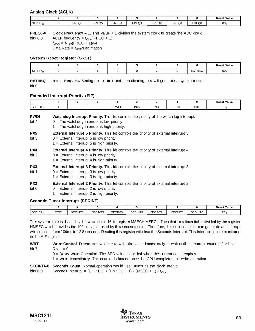
MSC1211 65SBAS267 www.ti.com
Analog Clock (ACLK)
FREQ6-0 Clock Frequency – 1. This value + 1 divides the system clock to create the ADC clock.bits 6-0 ACLK frequency = fCLK/(FREQ + 1)
fMOD = fCLK/(FREQ + 1)/64Data Rate = fMOD/Decimation
System Reset Register (SRST)
7 6 5 4 3 2 1 0 Reset Value
SFR F8H 1 1 1 PWDI PX5 PX4 PX3 PX2 E0H
7 6 5 4 3 2 1 0 Reset Value
SFR F9H WRT SECINT6 SECINT5 SECINT4 SECINT3 SECINT2 SECINT1 SECINT0 7FH
This system clock is divided by the value of the 16-bit register MSECH:MSECL. Then that 1ms timer tick is divided by the registerHMSEC which provides the 100ms signal used by this seconds timer. Therefore, this seconds timer can generate an interruptwhich occurs from 100ms to 12.8 seconds. Reading this register will clear the Seconds Interrupt. This Interrupt can be monitoredin the AIE register.
WRT Write Control. Determines whether to write the value immediately or wait until the current count is finished.bit 7 Read = 0.
0 = Delay Write Operation. The SEC value is loaded when the current count expires.1 = Write Immediately. The counter is loaded once the CPU completes the write operation.
SECINT6-0 Seconds Count. Normal operation would use 100ms as the clock interval.bits 6-0 Seconds Interrupt = (1 + SEC) • (HMSEC + 1) • (MSEC + 1) • tCLK.
7 6 5 4 3 2 1 0 Reset Value
SFR F7H 0 0 0 0 0 0 0 RSTREQ 00H
7 6 5 4 3 2 1 0 Reset Value
SFR F6H 0 FREQ6 FREQ5 FREQ4 FREQ3 FREQ2 FREQ1 FREQ0 03H
RSTREQ Reset Request. Setting this bit to 1 and then clearing to 0 will generate a system reset.bit 0
Extended Interrupt Priority (EIP)
PWDI Watchdog Interrupt Priority. This bit controls the priority of the watchdog interrupt.bit 4 0 = The watchdog interrupt is low priority.
1 = The watchdog interrupt is high priority.
PX5 External Interrupt 5 Priority. This bit controls the priority of external interrupt 5.bit 3 0 = External interrupt 5 is low priority.
1 = External interrupt 5 is high priority.
PX4 External Interrupt 4 Priority. This bit controls the priority of external interrupt 4.bit 2 0 = External interrupt 4 is low priority.
1 = External interrupt 4 is high priority.
PX3 External Interrupt 3 Priority. This bit controls the priority of external interrupt 3.bit 1 0 = External interrupt 3 is low priority.
1 = External interrupt 3 is high priority.
PX2 External Interrupt 2 Priority. This bit controls the priority of external interrupt 2.bit 0 0 = External interrupt 2 is low priority.
1 = External interrupt 2 is high priority.
Seconds Timer Interrupt (SECINT)

MSC121166SBAS267www.ti.com
The clock used for this timer is the 1ms clock which results from dividing the system clock by the values in registers MSECH:MSECL.Reading this register will clear the interrupt.
WRT Write Control. Determines whether to write the value immediately or wait until the current count is finished. Read = 0.bit 7 0 = Delay Write Operation. The MSINT value is loaded when the current count expires.
1 = Write Immediately. The MSINT counter is loaded once the CPU completes the write operation.
MSINT6-0 Seconds Count. Normal operation would use 1ms as the clock interval.bits 6-0 MS Interrupt Interval = (1 + MSINT) • (MSEC + 1) • tCLK
One Microsecond Register (USEC)
FREQ4-0 Clock Frequency – 1. This value + 1 divides the system clock to create a 1µs Clock.bits 4-0 USEC = CLK/(FREQ + 1). This clock is used to set Flash write time. See FTCON (SFR EFH).
One Millisecond Low Register (MSECL)
MSECL7-0 One Millisecond Low. This value in combination with the next register is used to create a 1ms Clock.bits 7-0 1ms Clock = (MSECH • 256 + MSECL + 1) • tCLK. This clock is used to set Flash erase time. See FTCON (SFR EFH).
One Millisecond High Register (MSECH)
7 6 5 4 3 2 1 0 Reset Value
SFR FAH WRT MSINT6 MSINT5 MSINT4 MSINT3 MSINT2 MSINT1 MSINT0 7FH
Milliseconds Interrupt (MSINT)
7 6 5 4 3 2 1 0 Reset Value
SFR FBH 0 0 0 FREQ4 FREQ3 FREQ2 FREQ1 FREQ0 03H
7 6 5 4 3 2 1 0 Reset Value
SFR FDH MSECH7 MSECH6 MSECH5 MSECH4 MSECH3 MSECH2 MSECH1 MSECH0 0FH
7 6 5 4 3 2 1 0 Reset Value
SFR FCH MSECL7 MSECL6 MSECL5 MSECL4 MSECL3 MSECL2 MSECL1 MSECL0 9FH
MSECH7-0 One Millisecond High. This value in combination with the previous register is used to create a 1ms clock.bits 7-0 1ms = (MSECH • 256 + MSECL + 1) • tCLK.
One Hundred Millisecond Register (HMSEC)
7 6 5 4 3 2 1 0 Reset Value
SFR FEH HMSEC7 HMSEC6 HMSEC5 HMSEC4 HMSEC3 HMSEC2 HMSEC1 HMSEC0 63H
7 6 5 4 3 2 1 0 Reset Value
SFR FFH EWDT DWDT RWDT WDCNT4 WDCNT3 WDCNT2 WDCNT1 WDCNT0 00H
HMSEC7-0 One Hundred Millisecond. This clock divides the 1ms clock to create a 100ms clock.bits 7-0 100ms = (MSECH • 256 + MSECL + 1) • (HMSEC + 1) • tCLK.
Watchdog Timer Register (WDTCON)
EWDT Enable Watchdog (R/W).bit 7 Write 1/Write 0 sequence sets the Watchdog Enable Counting bit.
DWDT Disable Watchdog (R/W).bit 6 Write 1/Write 0 sequence clears the Watchdog Enable Counting bit.
RWDT Reset Watchdog (R/W).bit 5 Write 1/Write 0 sequence restarts the Watchdog Counter.
WDCNT4-0 Watchdog Count (R/W).bits 4-0 Watchdog expires in (WDCNT + 1) • HMSEC to (WDCNT + 2) • HMSEC, if the sequence is not asserted. There
is an uncertainty of 1 count.

MSC1211 67SBAS267 www.ti.com
PACKAGE DRAWING MTQF006A – JANUARY 1995 – REVISED DECEMBER 1996
PAG (S-PQFP-G64) PLASTIC QUAD FLATPACK
0,13 NOM
0,25
0,450,75
Seating Plane
0,05 MIN
4040282/C 11/96
Gage Plane
33
0,170,27
16
48
1
7,50 TYP
49
64
SQ
9,80
1,050,95
11,8012,20
1,20 MAX
10,20SQ
17
32
0,08
0,50 M0,08
0°–7°
NOTES: A. All linear dimensions are in millimeters.B. This drawing is subject to change without notice.C. Falls within JEDEC MS-026

IMPORTANT NOTICE
Texas Instruments Incorporated and its subsidiaries (TI) reserve the right to make corrections, modifications,enhancements, improvements, and other changes to its products and services at any time and to discontinueany product or service without notice. Customers should obtain the latest relevant information before placingorders and should verify that such information is current and complete. All products are sold subject to TI’s termsand conditions of sale supplied at the time of order acknowledgment.
TI warrants performance of its hardware products to the specifications applicable at the time of sale inaccordance with TI’s standard warranty. Testing and other quality control techniques are used to the extent TIdeems necessary to support this warranty. Except where mandated by government requirements, testing of allparameters of each product is not necessarily performed.
TI assumes no liability for applications assistance or customer product design. Customers are responsible fortheir products and applications using TI components. To minimize the risks associated with customer productsand applications, customers should provide adequate design and operating safeguards.
TI does not warrant or represent that any license, either express or implied, is granted under any TI patent right,copyright, mask work right, or other TI intellectual property right relating to any combination, machine, or processin which TI products or services are used. Information published by TI regarding third–party products or servicesdoes not constitute a license from TI to use such products or services or a warranty or endorsement thereof.Use of such information may require a license from a third party under the patents or other intellectual propertyof the third party, or a license from TI under the patents or other intellectual property of TI.
Reproduction of information in TI data books or data sheets is permissible only if reproduction is withoutalteration and is accompanied by all associated warranties, conditions, limitations, and notices. Reproductionof this information with alteration is an unfair and deceptive business practice. TI is not responsible or liable forsuch altered documentation.
Resale of TI products or services with statements different from or beyond the parameters stated by TI for thatproduct or service voids all express and any implied warranties for the associated TI product or service andis an unfair and deceptive business practice. TI is not responsible or liable for any such statements.
Mailing Address:
Texas InstrumentsPost Office Box 655303Dallas, Texas 75265
Copyright 2003, Texas Instruments Incorporated