sbos246d – june 2002 – revised april 2005 precision ... – june 2002 – revised april 2005...
TRANSCRIPT

LOG112LOG2112
SBOS246D – JUNE 2002 – REVISED APRIL 2005
www.ti.com
DESCRIPTIONThe LOG112 and LOG2112 are versatile integrated circuitsthat compute the logarithm or log ratio of an input currentrelative to a reference current. VLOGOUT of the LOG112 andLOG2112 are trimmed to 0.5V per decade of input current,ensuring high precision over a wide dynamic range of inputsignals.
The LOG112 and LOG2112 features a 2.5V voltage refer-ence that may be used to generate a precision currentreference using an external resistor.
Low DC offset voltage and temperature drift allow accuratemeasurement of low-level signals over the specified tem-perature range of –5°C to +75°C.
FEATURES EASY-TO-USE COMPLETE FUNCTION
OUTPUT SCALING AMPLIFIER
ON-CHIP 2.5V VOLTAGE REFERENCE
HIGH ACCURACY: 0.2% FSO Over 5 Decades
WIDE INPUT DYNAMIC RANGE:7.5 Decades, 100pA to 3.5mA
LOW QUIESCENT CURRENT: 1.75mA
WIDE SUPPLY RANGE: ±4.5V to ±18V
PACKAGES: SO-14 (narrow) and SO-16
PRODUCTION DATA information is current as of publication date.Products conform to specifications per the terms of Texas Instrumentsstandard warranty. Production processing does not necessarily includetesting of all parameters.
Copyright © 2002-2005, Texas Instruments Incorporated
PrecisionLOGARITHMIC AND LOG RATIO AMPLIFIERS
Please be aware that an important notice concerning availability, standard warranty, and use in critical applications ofTexas Instruments semiconductor products and disclaimers thereto appears at the end of this data sheet.
APPLICATIONS LOG, LOG RATIO:
Communication, Analytical, Medical, Industrial,Test, General Instrumentation
PHOTODIODE SIGNAL COMPRESSION AMP
ANALOG SIGNAL COMPRESSION IN FRONTOF ANALOG-TO-DIGITAL (A/D) CONVERTER
ABSORBANCE MEASUREMENT
OPTICAL DENSITY MEASUREMENT
LOG112
LOG2112
A2A1
Q1 Q2
CC
I1
VREF – GND
NOTE: Internal resistors are used to compensate gain change over temperature.The VCM pin is internally connected to GND in the LOG2112.
VO3
V+
GND
LOG112
VLOGOUT = (0.5V)LOG (I1/I2)
VO3 = K (0.5V)LOG (I1/I2), K = 1 + R2/R1
A3
R2R1
VREF
RREF
+IN3VLOGOUT–IN3
V–VCM
I2
VREF
All trademarks are the property of their respective owners.
LOG112, 21122SBOS246Dwww.ti.com
ABSOLUTE MAXIMUM RATINGS(1)
Supply Voltage, V+ to V– .................................................................. ±18V
Inputs ................................................................................................. ±18VInput Current ................................................................................... ±10mA
Output Short-Circuit Current(2) ................................................ Continuous
Operating Temperature ....................................................–40°C to +85°CStorage Temperature ..................................................... –55°C to +125°CJunction Temperature .................................................................... +150°CLead Temperature (soldering, 10s) ............................................... +300°C
NOTES: (1) Stresses above these ratings may cause permanent damage.Exposure to absolute maximum conditions for extended periods may degradedevice reliability. (2) One output per package.
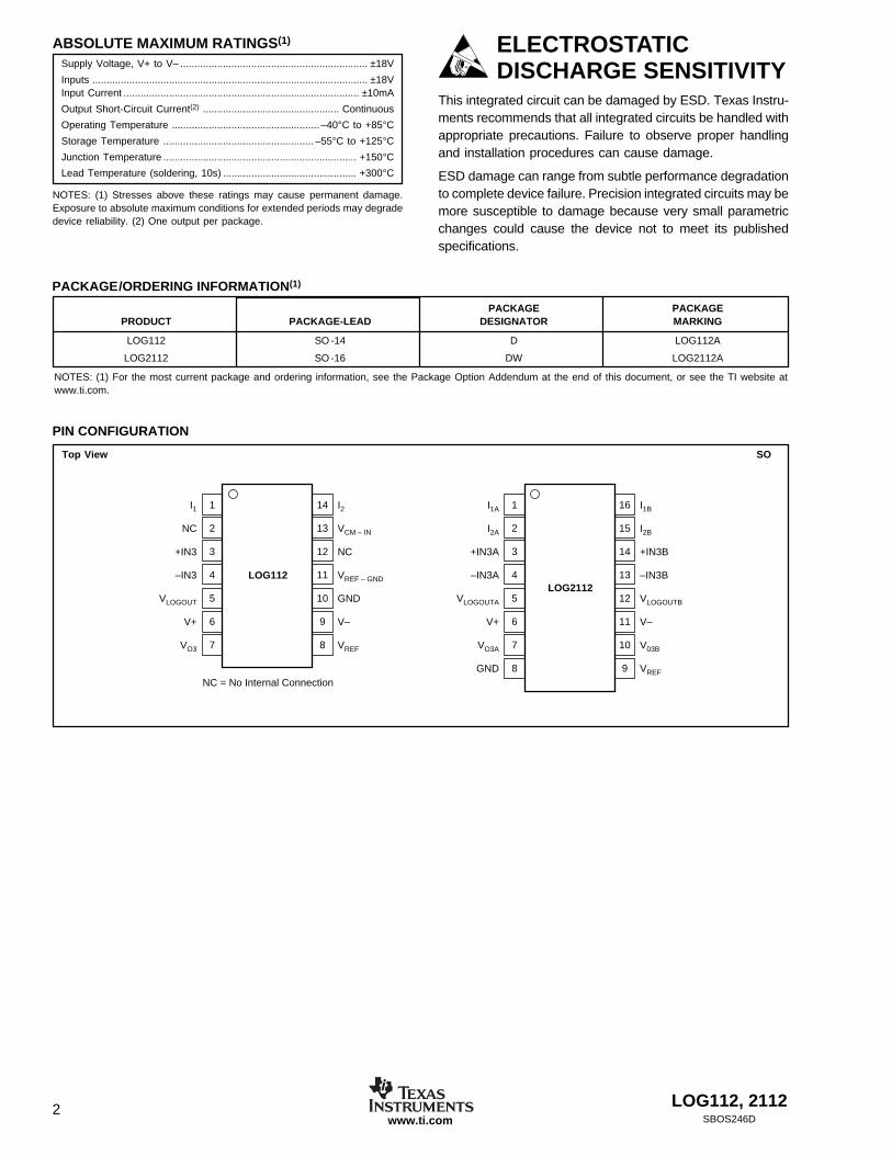
PIN CONFIGURATION
Top View SO
I2
VCM – IN
NC
VREF – GND
GND
V–
VREF
NC = No Internal Connection
LOG112
I1
NC
+IN3
–IN3
VLOGOUT
V+
VO3
14
13
12
11
10
9
8
1
2
3
4
5
6
7
I1B
I2B
+IN3B
–IN3B
VLOGOUTB
V–
V03B
VREF
LOG2112
I1A
I2A
+IN3A
–IN3A
VLOGOUTA
V+
VO3A
GND
16
15
14
13
12
11
10
9
1
2
3
4
5
6
7
8
ELECTROSTATICDISCHARGE SENSITIVITY
This integrated circuit can be damaged by ESD. Texas Instru-ments recommends that all integrated circuits be handled withappropriate precautions. Failure to observe proper handlingand installation procedures can cause damage.
ESD damage can range from subtle performance degradationto complete device failure. Precision integrated circuits may bemore susceptible to damage because very small parametricchanges could cause the device not to meet its publishedspecifications.
PACKAGE PACKAGEPRODUCT PACKAGE-LEAD DESIGNATOR MARKING
LOG112 SO -14 D LOG112A
LOG2112 SO -16 DW LOG2112A
NOTES: (1) For the most current package and ordering information, see the Package Option Addendum at the end of this document, or see the TI website atwww.ti.com.
PACKAGE/ORDERING INFORMATION(1)
LOG112, 2112 3SBOS246D www.ti.com
ELECTRICAL CHARACTERISTICSBoldface limits apply over the specified temperature range, TA = –5°C to +75°C.At TA = +25°C, VS = ±5V, and ROUT = 10kΩ, unless otherwise noted.
LOG112, LOG2112
PARAMETER CONDITION MIN TYP MAX UNITS
CORE LOG FUNCTIONVIN /VOUT Equation VLOGOUT = (0.5V)LOG (I1/I2) V
LOG CONFORMITY ERROR(1)
Initial 1nA to 100µA (5 decades) 0.01 0.2 %100pA to 3.5mA (7.5 decades) 0.13 %
over Temperature 1nA to 100µA (5 decades) 0.0001 %/°C100pA to 3.5mA (7.5 decades) 0.005 %/°C
GAIN(2)
Initial Value 1nA to 100µA 0.5 V/decadeGain Error 1nA to 100µA 0.10 ±1 %
vs Temperature TMIN to TMAX 0.003 0.01 %/°CINPUT, A1A and A1B, A2A, A2B
Offset Voltage ±0.3 ±1.5 mVvs Temperature TMIN to TMAX ±2 µV/°Cvs Power Supply (PSRR) VS = ±4.5V to ±18V 5 20 µV/V
Input Bias Current ±5 pAvs Temperature TMIN to TMAX Doubles Every 10°C
Voltage Noise f = 10Hz to 10kHz 3 µVrmsf = 1kHz 30 nV/√Hz
Current Noise f = 1kHz 4 fA/√HzCommon-Mode Voltage Range (Positive) (V+) – 2 (V+) – 1.5 V
(Negative) (V–) + 2 (V–) + 1.2 VCommon-Mode Rejection Ratio (CMRR) 10 µV/V
OUTPUT, (VLOG OUT) A2A, A2BOutput Offset, VOSO, Initial ±3 ±15 mV
vs Temperature TMIN to TMAX ±10 µV/°CFull-Scale Output (FSO) VS = ±5V (V–) + 1.2 (V+) – 1.5 VShort-Circuit Current ±18 mA
TOTAL ERROR(3)(4) I1 or I2 remains fixed while other varies.Initial Min to Max
I1 or I2 = 5mA (VS ≥ ±6V) ±150 mVI1 or I2 = 3.5mA ±75 mVI1 or I2 = 1mA ±20 mV
I1 or I2 = 100µA ±20 mVI1 or I2 = 10µA ±20 mVI1 or I2 = 1µA ±20 mV
I1 or I2 = 100nA ±20 mVI1 or I2 = 10nA ±20 mVI1 or I2 = 1nA ±20 mV
I1 or I2 = 350pA ±20 mVI1 or I2 = 100pA ±20 mV
vs Temperature I1 or I2 = 3.5mA ±1.2 mV/°CI1 or I2 = 1mA ±0.4 mV/°C
I1 or I2 = 100µA ±0.1 mV/°CI1 or I2 = 10µA ±0.05 mV/°CI1 or I2 = 1µA ±0.05 mV/°C
I1 or I2 = 100nA ±0.09 mV/°CI1 or I2 = 10nA ±0.2 mV/°CI1 or I2 = 1nA ±0.3 mV/°C
I1 or I2 = 350pA ±0.1 mV/°CI1 or I2 = 100pA ±0.3 mV/°C
vs Supply I1 or I2 = 3.5mA ±3.0 mV/VI1 or I2 = 1mA ±0.1 mV/V
I1 or I2 = 100µA ±0.1 mV/VI1 or I2 = 10µA ±0.1 mV/VI1 or I2 = 1µA ±0.1 mV/V
I1 or I2 = 100nA ±0.1 mV/VI1 or I2 = 10nA ±0.1 mV/VI1 or I2 = 1nA ±0.25 mV/V
I1 or I2 = 350pA ±0.1 mV/VI1 or I2 = 100pA ±0.1 mV/V
NOTES: (1) Log Conformity Error is the peak deviation from the best-fit-straight line of VO versus LOG (I1/I2) curve expressed as a percent of peak-to-peak full-scale output. K, scale factor, equals 0.5V output per decade of input current. (2) Scale factor of core log function is trimmed to 0.5V output per decade change ofinput current. (3) Worst-case Total Error for any ratio of I1/I2, as the largest of the two errors, when I1 and I2 are considered separately. (4) Total Error includes offsetvoltage, bias current, gain, and log conformity. (5) Bandwidth (3dB) and transient response are a function of both the compensation capacitor and the level of inputcurrent.

LOG112, 21124SBOS246Dwww.ti.com
FREQUENCY RESPONSE, CORE LOG(5)
BW, 3dBI2 = 10nA CC = 4500pF 0.1 kHI2 = 1µA CC = 150pF 38 kHI2 = 10µA CC = 150pF 40 kHI2 = 1mA CC = 50pF 45 kHz
Step ResponseIncreasing
I1 = 10nA to 100nA CC = 120pF, I2 = 31.6nA 1.1 msI1 = 1µA to 100µA CC = 375pF, I2 = 10µA 1.6 µsI1 = 1µA to 1mA CC = 950pF, I2 = 31.6µA 1.5 µs
DecreasingI1 = 100nA to 10nA CC = 120pF, I2 = 31.6nA 2.1 msI1 = 100µA to 1µA CC = 375pF, I2 = 10µA 31.2 µsI1 = 1mA to 1µA CC = 950pF, I2 = 31.6µA 39 µs
IncreasingI2 = 10nA to 100nA CC = 125pF, I1 = 31.6nA 2.6 msI2 = 1µA to 100µA CC = 750pF, I1 = 10µA 113 µsI2 = 1µA to 1mA CC = 10.5nF, I1 = 31.6µA 1.2 ms
DecreasingI2 = 100nA to 10nA CC = 125pF, I1 = 31.6nA 630 µsI2 = 100µA to 1µA CC = 750pF, I1 = 10µA 6.6 µsI2 = 1mA to 1µA CC = 10.5nF, I1 = 31.6µA 13.3 µs
OP AMP, A3Input Offset Voltage +250 ±1000 µV
vs Temperature TMIN to TMAX ±2 µV/°Cvs Supply VS = ±4.5V to ±18V 5 50 µV/V
Input Bias Current –10 nAInput Offset Current ±0.5 nAInput Voltage Range (V–) (V+) – 1.5 VInput Noise, f = 0.1Hz to 10Hz 1 µVPP
f = 1kHz 28 nV/√HzOpen-Loop Voltage Gain 88 dBGain-Bandwidth Product 1.4 MHzSlew Rate 0.5 V/µsSettling Time, 0.01% G = –1, 3V Step, CL = 100pF 16 µsRated Output (V–) + 1.5 (V+) – 0.9 VShort-Circuit Current ±4 mA
VOLTAGE REFERENCEBandgap Voltage 2.5 VError, Initial ±0.05 ±0.5 %
vs Temperature TMIN to TMAX ±25 ppm/°Cvs Supply VS = ±4.5V to ±18V ±10 ppm/Vvs Load ILOAD = 10mA ±600 ppm/mA
Short-Circuit Current 16 mA
POWER SUPPLYOperating Range VS ±4.5 ±18 VQuiescent Current IO = 0LOG112 ±1.25 ±1.75 mALOG2112 ±2.5 ±3.5 mA
TEMPERATURE RANGESpecified Range, TMIN to TMAX –5 75 °COperating Range –40 85 °CStorage Range –55 125 °CThermal Resistance, θJA SO-14 110 °C/W
SO-16 80 °C/W
NOTES: (1) Log Conformity Error is the peak deviation from the best-fit-straight line of VO vs LOG(I1/I2) curve expressed as a percent of peak-to-peak full-scaleoutput. K, scale factor, equals 0.5V output per decade of input current. (2) Scale factor of core log function is trimmed to 0.5V output per decade change of inputcurrent. (3) Worst-case Total Error for any ratio of I1/I2, as the largest of the two errors, when I1 and I2 are considered separately. (4) Total Error includes offsetvoltage, bias current, gain, and log conformity. (5) Bandwidth (3dB) and transient response are a function of both the compensation capacitor and the level of inputcurrent.
ELECTRICAL CHARACTERISTICS (Cont.)Boldface limits apply over the specified temperature range, TA = –5°C to +75°C.At TA = +25°C, VS = ±5V, and RL = 10kΩ, unless otherwise noted.
LOG112, LOG2112
PARAMETER CONDITION MIN TYP MAX UNITS
LOG112, 2112 5SBOS246D www.ti.com
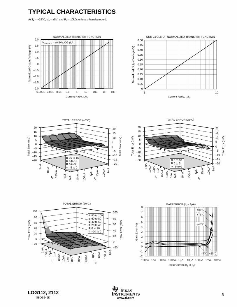
TYPICAL CHARACTERISTICSAt TA = +25°C, VS = ±5V, and RL = 10kΩ, unless otherwise noted.
2.0
1.5
1.0
0.5
0
–0.5
–1.0
–1.5
–2.0
Nor
mal
ized
Out
put V
olta
ge (
V)
NORMALIZED TRANSFER FUNCTION
0.0001 0.001 0.01 0.1 1 10 100 1k 10k
Current Ratio, I1/I2
VLOGOUT = (0.5V)LOG (I1/I2)
ONE CYCLE OF NORMALIZED TRANSFER FUNCTION
Nor
mal
ized
Out
put V
olta
ge (
V)
0.50
0.45
0.40
0.35
0.30
0.25
0.20
0.15
0.10
0.05
01 10
Current Ratio, I1/I2
8
7
6
5
4
3
2
1
0
–1
–21nA 10nA 100nA 1µA 10µA 100µA 1mA 10mA100pA
GAIN ERROR (I2 = 1µA)
Input Current (I1 or I2)
Gai
n E
rror
(%
) –40°C
+75°C
–5°C +25°C
+85°C
–20
–15
–10
–5
0
5
10
15
20
–20
–15
–10–5
0
510
15
20
1mA
10µA
100n
A
1nA
10nA
100n
A
1µA
10µA
100µ
A
1mA
1nA
I1 I2
Tot
al E
rror
(m
V)
TOTAL ERROR (–5°C)
Tot
al E
rror
(m
V)
10 to 155 to 100 to 5–5 to 0
–20
–15
–10
–5
0
5
10
15
20
–20
–15
–10–5
0
510
15
20
1mA
10µA
100µ
A
1µA
100n
A
1nA
10nA
100n
A
1µA
10µA
100µ
A
1mA
10nA
1nA
I1 I2
Tot
al E
rror
(m
V)
Tot
al E
rror
(m
V)
5 to 100 to 5–5 to 0
TOTAL ERROR (25°C)
–20
20
0
40
60
80
100
–20
0
20
40
60
80
100
1mA
10µA
100µ
A
1µA
100n
A
1nA
10nA
100n
A
1µA
10µA
100µ
A
1mA
10nA
1nA
I1 I2
Tot
al E
rror
(m
V)
Tot
al E
rror
(m
V)
20 to 400 to 20
40 to 6060 to 8080 to 100
–20 to 0
TOTAL ERROR (70°C)
LOG112, 21126SBOS246Dwww.ti.com
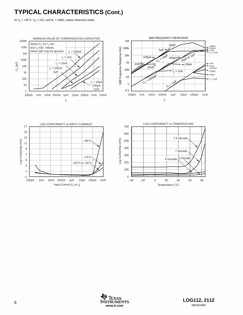
TYPICAL CHARACTERISTICS (Cont.)At TA = +25°C, VS = ±5V, and RL = 10kΩ, unless otherwise noted.
MINIMUM VALUE OF COMPENSATION CAPACITOR100M
10M
1M
100k
10k
1k
100
10
1
CC (
pF)
100pA 1nA 10nA 100nA 1µA 10µA 100µA 1mA 10mA
I2
I1 = 100pA
I1 = 1nA
I1 = 10nA
I1 = 100nA1µA
I1 = 10µA100µA1mA
Select CC for I1 min.and I2 max. Values below 2pF may be ignored.
3dB FREQUENCY RESPONSE
3dB
Fre
quen
cy R
espo
nse
(Hz)
0.1
1M
100k
10k
1k
100
10
1
100µA100µA1mAI1 = 1mA
1µA1mA to 10µA
100nA
10nA
I1 = 1nA
10nA
C C = 1000pF
C C = 1µF
10µA to 1µA
C C = 10pF
1nA
100µA
100pA 1nA 10nA 100nA 1µA 10µA 100µA 1mA
I2
1µA
10µA
100µA
I1 = 1nA10nA
17
15
13
11
9
7
5
3
1
–1
Input Current (I1 or I2)
Log
Con
form
ity (
mV
)
LOG CONFORMITY vs INPUT CURRENT
+85°C
+75°C
–40°C to +25°C
100pA 1nA 10nA 100nA 1µA 10µA 100µA 1mA
LOG CONFORMITY vs TEMPERATURELo
g C
onfo
rmity
(m
%)
700
600
500
400
300
200
100
0–40 –20 0 20 40 60 80
Temperature (°C)
7.5 Decade
7 Decade
6 Decade 5 Decade
LOG112, 2112 7SBOS246D www.ti.com
FIGURE 1. Basic Connections of the LOG112.
APPLICATION INFORMATIONThe LOG112 is a true logarithmic amplifier that uses thebase-emitter voltage relationship of bipolar transistors tocompute the logarithm, or logarithmic ratio of a current ratio.
Figure 1 and Figure 2 show the basic connections requiredfor operation of the LOG112 and LOG2112. In order toreduce the influence of lead inductance of power-supplylines, it is recommended that each supply be bypassed witha 10µF tantalum capacitor in parallel with a 1000pF ceramiccapacitor, as shown in Figure 1 and Figure 2. Connectingthe capacitors as close to the LOG112 and LOG2112 aspossible will contribute to noise reduction as well.
INPUT CURRENT RANGE
To maintain specified accuracy, the input current range of theLOG112 and LOG2112 should be limited from 100pA to3.5mA. Input currents outside of this range may compromisethe LOG112 performance. Input currents larger than 3.5mAresult in increased nonlinearity. An absolute maximum inputcurrent rating of 10mA is included to prevent excessive powerdissipation that may damage the input transistor.
On ±5V supplies, the total input current (I1 + I2) is limited to4.5mA. Due to compliance issues internal to the LOG112 andLOG2112, to accommodate larger total input currents, suppliesshould be increased.
SETTING THE REFERENCE CURRENT
When the LOG112 and LOG2112 are used to compute loga-rithms, either I1 or I2 can be held constant to become thereference current to which the other is compared.
VLOGOUT is expressed as:
VLOGOUT = (0.5V)LOG (I1/IREF) (1)
IREF can be derived from an external current source (such asthat shown in Figure 3), or it may be derived from a voltagesource with one or more resistors. When a single resistor isused, the value may be large depending on IREF. If IREF is10nA and +2.5V is used:
RREF = 2.5V/10nA = 250MΩ (2)
14
1
5
8
6
9 10 13
V–
V+
10µF
LOG112
1000pF
10µF 1000pF
I1 I2
VLOGOUT
VREF
11 VREF – GND
VCM – IN
CC
15
16
56
11 8
V–
V+
10µF
LOG2112
1000pF
10µF 1000pF
I1B I2B
1
2
I2A I1A
VLOGOUTA9 VREF
12VLOGOUTB
CCB
CCA
FIGURE 2. Basic Connections of the LOG2112.
FIGURE 3. Temperature Compensated Current Source.
2N2905
IREF
RREF
2N2905
+15V –15V
IREF = 6V
RREF
3.6kΩ
6VIN834
FIGURE 4. T Network for Reference Current.
A1
+
R2
R1
+5V
R3
VREF = 100mV
R3 >> R2
IREF
–VOS
1
A voltage divider may be used to reduce the value of theresistor, as shown in Figure 4. When using this method, onemust consider the possible errors caused by the amplifier’sinput offset voltage. The input offset voltage of amplifier A1
has a maximum value of 1.5mV, making VREF a suggestedvalue of 100mV.
LOG112, 21128SBOS246Dwww.ti.com
FIGURE 7. Precision Current Inverter/Current Source.
Figure 5 shows a low-level current source using a seriesresistor. The low offset op amp reduces the effect of theLOG112 and LOG2112’s input offset voltage.
FREQUENCY COMPENSATION
Frequency compensation for the LOG112 is obtained byconnecting a capacitor between pins 5 and 14. Frequencycompensation for the LOG2112 is obtained by connecting acapacitor between pins 2 and 5, or 15 and 12. The size of thecapacitor is a function of the input currents, as shown in theTypical Characteristic curves (Minimum Value of Compensa-tion Capacitor). For any given application, the smallest valueof the capacitor which may be used is determined by themaximum value of I2 and the minimum value of I1. Largervalues of CC make the LOG112 and LOG2112 more stable,but reduce the frequency response.
In an application, highest overall bandwidth can be achievedby detecting the signal level at VOUT, then switching inappropriate values of compensation capacitors.
NEGATIVE INPUT CURRENTS
The LOG112 and LOG2112 function only with positive inputcurrents (conventional current flows into input current pins).In situations where negative input currents are needed, thecircuits in Figures 6, 7, and 8 may be used.FIGURE 5. Current Source with Offset Compensation.
1MΩ+2.5mV
100kΩ
–2.5V
+2.5V
OPA335
100Ω
I1 = 2.5nA to 1mA
I2 = 2.5nA
VLOGOUT
CC
14
1
9 10
V–
LOG112
65
V+
8
VREF
Chopper Op Amp
GND
FIGURE 6. Current Inverter/Current Source.
QB
NationalLM394
IIN
IOUT
D1
OPA703
D2
QA
FREQUENCY RESPONSE
The frequency response curves seen in the Typical Charac-teristic curves are shown for constant DC I1 and I2 with asmall-signal AC current on one input.
The 3dB frequency response of the LOG112 and LOG2112 area function of the magnitude of the input current levels and of thevalue of the frequency compensation capacitor. See TypicalCharacteristic curve, 3dB Frequency Response for details.
The transient response of the LOG112 and LOG2112 aredifferent for increasing and decreasing signals. This is due tothe fact that a log amp is a nonlinear gain element and hasdifferent gains at different levels of input signals. Smallerinput currents require greater gain to maintain full dynamicrange, and will slow the frequency response of the LOG112and LOG2112.
1.5kΩ
Photodiode
10nA to 1mA
10nA to 1mA
+5V
+5V1kΩ
+3.3V(1)
1/2OPA2335
1/2OPA2335
BSH203
TLV271 or 1/2 OPA2335
(+3.3VBack Bias)
LOG112
Pin 1 or Pin 14
NOTE: (1) +3.3V bias is an arbitrary ac level < 5V that also appears on the −IN through the op amp where it applies a reverse bias to the photodiode.

LOG112, 2112 9SBOS246D www.ti.com
FIGURE 8. Precision Current Inverter/Current Source.
1kΩ
+5V
+5V 1.5kΩ
1.5kΩ
100kΩ
10nA to 1mA
LOG11210nA to 1mA
100kΩ
100kΩ
(+3.3V Back Bias)
+3.3V(1)
1/2OPA2335
1/2OPA2335
Photodiode
Pin 1 or Pin 14
100kΩNOTE: (1) +3.3V bias is an arbitrary dc level < 5V that also appears on the −IN through the op amp where it applies a reverse bias to the photodiode.
VOLTAGE INPUTS
The LOG112 and LOG2112 give the best performances withcurrent inputs. Voltage inputs may be handled directly withseries resistors, but the dynamic input range is limited toapproximately three decades of input voltage by voltagenoise and offsets. The transfer function of Equation 13applies to this configuration.
ACHIEVING HIGHER ACCURACY WITH HIGHERINPUT CURRENTS
As input current to the LOG112 increases, output accuracydegrades. For a 4.5mA input current on ±5V supplies and a10mA input current on ±12V supplies, total output error canbe between 15% and 25%. Applying a common-mode volt-
age to VCM of at least +1V and up to 2.5V, brings the logtransistors out of saturation and reduces output error toapproximately 10%. To avoid forward biasing a photodiode,return the cathode to the VCM pin, as shown in Figure 9. Toreverse bias the photodiode, apply a more positive voltage tothe cathode than the anode.
APPLICATION CIRCUITSLOG RATIO
One of the more common uses of log ratio amplifiers isto measure absorbance. See Figure 10 for a typical application.
Absorbance of the sample is A = logλ1´/ λ1 (3)
If D1 and D2 are matched A ∝ (0.5V) logI1/ I2 (4)
FIGURE 9. Extending Input Current Level and Improving Accuracy by Applying a Common-Mode Voltage.
A2A1
Q1 Q2
CC
I1
VREF – GND
VO3
V+ = +5V
GND
LOG112
A3
R2R1
VREF100kΩ
+2.5V
150kΩ
RREF
+IN3VLOGOUT–IN3
V– = –5VVCM
I2
VREF
6 5 3 4
7
9101311
8
14
1
+1.5V
LOG112, 211210SBOS246Dwww.ti.com
FIGURE 11. Single +5V Power-Supply Operation.
14
1 5
10
6
9
12
3 5
4
–5V
1µF
LOG112
1µF
I1
I2
VLOGOUT
CC
1µF
TPS(1)
Single Supply +5V
NOTE: (1) TPS60402DBVnegative charge pump.
FIGURE 10. Absorbance Measurement.
I2
I1
14
1
9
10
5VLOGOUT
6
V+
V–
CC
LOG112
D2
D1Sample
λ 1λ 1´
λ 1LightSource
DATA COMPRESSION
In many applications, the compressive effects of the logarith-mic transfer function are useful. For example, a LOG112preceding a 12-bit A/D converter can produce the dynamicrange equivalent to a 20-bit converter.
OPERATION ON SINGLE SUPPLY
Many applications do not have the dual supplies required tooperate the LOG112 and LOG2112. Figure 11 shows theLOG112 and LOG2112 configured for operation with a single+5V supply.
MEASURING AVALANCHE PHOTODIODE CURRENT
The wide dynamic range of the LOG112 and LOG2112 isuseful for measuring avalanche photodiode current (APD), asshown in Figure 12.
FIGURE 12. High-Side Shunt for APD Measures 3 Decades of APD Current.
A1
–5V
SO-14
9 11 13
LOG112
Q1
2
Q2
IOUT
IOUT = 0.1 • ISHUNT
10 3
4
10kΩ
Receiver
Irx = 1µA to 1mA
I-to-VConverter
APD
10Gbits/sec
16.7kΩCC
A2
A3 V03 = 2.5V to 0V
ISHUNT500Ω
5kΩ 5kΩ
+15V to +60V
+5V
INA168SOT23-5
+5V
1
1
14
8
6 5
7
100µA 25kΩ
VREF
LOG112, 2112 11SBOS246D www.ti.com
also
V VR R
ROUT L= +1 2
1(9)
VR R
Rn V
IIOUT T= +1 2
1
1
2log (10)
or V V LOGIIOUT =
( . )0 5 1
2(11)
Using the base-emitter voltage relationship of matchedbipolar transistors, the LOG112 establishes a logarith-mic function of input current ratios. Beginning with thebase-emitter voltage defined as:
V VII
where VkTqBE T
C
ST= =ln : (1)
k = Boltzmann’s constant = 1.381 • 10–23
T = Absolute temperature in degrees Kelvin
q = Electron charge = 1.602 • 10–19 Coulombs
IC = Collector current
IS = Reverse saturation current
From the circuit in Figure 12:
V V VL BE BE= 1 2– (2)
Substituting (1) into (2) yields:
V VI
IV
I
IL TS
TS
= 11
12
2
2
ln – ln (3)
If the transistors are matched and isothermal andVTI = VT2, then (3) becomes:
V VII
IIL T
S S=
1
1 2ln – ln (4)
V VII
and ceL T= ln sin1
2(5)
ln . logx x= 2 3 10 (6)
V n VIIL T= log 1
2(7)
where n = 2.3 (8)
INSIDE THE LOG112
FIGURE 13. Simplified Model of a Log Amplifier.
A2
A1
I1
Q1 Q2
I2
I1
I2
+ +
– –
R2
VOUT
VL
R1
VBE1VBE2
VOUT = (0.5V)LOGI1I2
NOTE: R1 is a metal resistor used to compensate for gainover temperature.
DEFINITION OF TERMSTRANSFER FUNCTION
The ideal transfer function is:
VLOGOUT = (0.5V)LOG (I1/I2)
Figure 14 shows the graphical representation of the transferover valid operating range for the LOG112 and LOG2112.
ACCURACY
Accuracy considerations for a log ratio amplifier are some-what more complicated than for other amplifiers. This isbecause the transfer function is nonlinear and has twoinputs, each of which can vary over a wide dynamic range.The accuracy for any combination of inputs is determinedfrom the total error specification.
TOTAL ERROR
The total error is the deviation (expressed in mV) of the actualoutput from the ideal output of VLOGOUT = (0.5V)LOG (I1/I2).
Thus,
VLOGOUT(ACTUAL) = VLOGOUT(IDEAL) ± Total Error (6)
It represents the sum of all the individual components of errornormally associated with the log amp when operated in thecurrent input mode. The worst-case error for any given ratioof I1/I2 is the largest of the two errors when I1 and I2 areconsidered separately. Temperature can affect total error.
FIGURE 14. Transfer Function with Varying I2 and I1.
3.0
3.5
2.0
2.5
1.0
1.5
0.5
0
–3.0
–3.5
–2.0
–2.5
–1.0
–0.5
–1.5
1nA 10nA100nA
1µA10µA
100µA1mA 10mA
100pA
VO
UT
(V)
I 2 = 100pA
I 2 = 1nA
I 2 = 10nA
I 2 = 100nA
I 2 = 1µA
I 2 = 10µA
I 2 = 100µA
I 2 = 1mA
I1
VLOGOUT = (0.5V)LOG (I1/I2)
LOG112, 211212SBOS246Dwww.ti.com
ERRORS RTO AND RTI
As with any transfer function, errors generated by the func-tion may be Referred-to-Output (RTO) or Referred-to-Input(RTI). In this respect, log amps have a unique property: givensome error voltage at the log amp’s output, that error corre-sponds to a constant percent of the input regardless of theactual input level.
LOG CONFORMITY
For the LOG112 and LOG2112, log conformity is calculatedthe same as linearity and is plotted I1/I2 on a semi-log scale.In many applications, log conformity is the most importantspecification. This is true because bias current errors arenegligible (5pA compared to input currents of 100pA andabove) and the scale factor and offset errors may be trimmedto zero or removed by system calibration. This leaves logconformity as the major source of error.
Log conformity is defined as the peak deviation from the bestfit straight line of the VLOGOUT versus log (I1/I2) curve. This isexpressed as a percent of ideal full-scale output. Thus, thenonlinearity error expressed in volts over m decades is:
VLOGOUT (NONLIN) = 0.5V/dec • 2NmV (7)
where N is the log conformity error, in percent.
INDIVIDUAL ERROR COMPONENTS
The ideal transfer function with current input is:
V V LOGIILOGOUT = ( )
0 5 1
2. (8)
The actual transfer function with the major components oferror is:
V V KI II I
Nm VLOGOUTB
BOSO= ( ) ±( )
± ±0 5 1 1 1
2 2. log
––
∆ (9)
The individual component of error is:
∆K = gain error (0.10%, typ), as specified in the specifica-tion table.
IB1 = bias current of A1 (5pA, typ)IB2 = bias current of A2 (5pA, typ)
N = log conformity error (0.01%, 0.13%, typ)
0.01% for m = 5, 0.13% for m = 7.5
VOSO = output offset voltage (3mV, typ)
m = number of decades over which N is specified
For example, what is the error when:I1 = 1µA and I2 = 100nA (10)
(11)
V mV
V
LOGOUT = ±( ) −−
± ( )( ) ±
=
− −
− −0 5 0 00110 5 10
10 5 102 0 0001 5 3 0
0 505
6 12
7 12. . log•
•. .
.
Since the ideal output is 0.5V, the error as a percent of thereading is:
%.
.% . %error
V= • =0 5050 5
100 1 01 (12)
For the case of voltage inputs, the actual transfer function is:
(13)
V V K
VR
IE
RVR
IE
R
Nm VLOGOUT
BOS
BOS
OSO= ( ) ±( )±
±
± ±0 5 1
1
1 1
2
2 2
11
22
. log–
–∆
Where ER
andER
OS OS1
1
2
2 (offset error) are considered to be
zero for large values of resistance from external input currentsources.

PACKAGE OPTION ADDENDUM
www.ti.com 22-Mar-2018
Addendum-Page 1
PACKAGING INFORMATION
Orderable Device Status(1)
Package Type PackageDrawing
Pins PackageQty
Eco Plan(2)
Lead/Ball Finish(6)
MSL Peak Temp(3)
Op Temp (°C) Device Marking(4/5)
Samples
LOG112AID ACTIVE SOIC D 14 50 Green (RoHS& no Sb/Br)
CU NIPDAU Level-3-260C-168 HR -40 to 85 LOG112A
LOG112AIDE4 ACTIVE SOIC D 14 50 Green (RoHS& no Sb/Br)
CU NIPDAU Level-3-260C-168 HR -40 to 85 LOG112A
LOG112AIDR ACTIVE SOIC D 14 2500 Green (RoHS& no Sb/Br)
CU NIPDAU Level-3-260C-168 HR -40 to 85 LOG112A
LOG2112AIDW ACTIVE SOIC DW 16 40 Green (RoHS& no Sb/Br)
CU NIPDAU Level-3-260C-168 HR -40 to 85 LOG2112A
LOG2112AIDWR ACTIVE SOIC DW 16 1000 Green (RoHS& no Sb/Br)
CU NIPDAU Level-3-260C-168 HR -40 to 85 LOG2112A
(1) The marketing status values are defined as follows:ACTIVE: Product device recommended for new designs.LIFEBUY: TI has announced that the device will be discontinued, and a lifetime-buy period is in effect.NRND: Not recommended for new designs. Device is in production to support existing customers, but TI does not recommend using this part in a new design.PREVIEW: Device has been announced but is not in production. Samples may or may not be available.OBSOLETE: TI has discontinued the production of the device.
(2) RoHS: TI defines "RoHS" to mean semiconductor products that are compliant with the current EU RoHS requirements for all 10 RoHS substances, including the requirement that RoHS substancedo not exceed 0.1% by weight in homogeneous materials. Where designed to be soldered at high temperatures, "RoHS" products are suitable for use in specified lead-free processes. TI mayreference these types of products as "Pb-Free".RoHS Exempt: TI defines "RoHS Exempt" to mean products that contain lead but are compliant with EU RoHS pursuant to a specific EU RoHS exemption.Green: TI defines "Green" to mean the content of Chlorine (Cl) and Bromine (Br) based flame retardants meet JS709B low halogen requirements of <=1000ppm threshold. Antimony trioxide basedflame retardants must also meet the <=1000ppm threshold requirement.
(3) MSL, Peak Temp. - The Moisture Sensitivity Level rating according to the JEDEC industry standard classifications, and peak solder temperature.
(4) There may be additional marking, which relates to the logo, the lot trace code information, or the environmental category on the device.
(5) Multiple Device Markings will be inside parentheses. Only one Device Marking contained in parentheses and separated by a "~" will appear on a device. If a line is indented then it is a continuationof the previous line and the two combined represent the entire Device Marking for that device.
(6) Lead/Ball Finish - Orderable Devices may have multiple material finish options. Finish options are separated by a vertical ruled line. Lead/Ball Finish values may wrap to two lines if the finishvalue exceeds the maximum column width.
PACKAGE OPTION ADDENDUM
www.ti.com 22-Mar-2018
Addendum-Page 2
Important Information and Disclaimer:The information provided on this page represents TI's knowledge and belief as of the date that it is provided. TI bases its knowledge and belief on informationprovided by third parties, and makes no representation or warranty as to the accuracy of such information. Efforts are underway to better integrate information from third parties. TI has taken andcontinues to take reasonable steps to provide representative and accurate information but may not have conducted destructive testing or chemical analysis on incoming materials and chemicals.TI and TI suppliers consider certain information to be proprietary, and thus CAS numbers and other limited information may not be available for release.
In no event shall TI's liability arising out of such information exceed the total purchase price of the TI part(s) at issue in this document sold by TI to Customer on an annual basis.
TAPE AND REEL INFORMATION
*All dimensions are nominal
Device PackageType
PackageDrawing
Pins SPQ ReelDiameter
(mm)
ReelWidth
W1 (mm)
A0(mm)
B0(mm)
K0(mm)
P1(mm)
W(mm)
Pin1Quadrant
LOG112AIDR SOIC D 14 2500 330.0 16.4 6.5 9.0 2.1 8.0 16.0 Q1
LOG2112AIDWR SOIC DW 16 1000 330.0 16.4 10.75 10.7 2.7 12.0 16.0 Q1
PACKAGE MATERIALS INFORMATION
www.ti.com 14-Jul-2012
Pack Materials-Page 1

*All dimensions are nominal
Device Package Type Package Drawing Pins SPQ Length (mm) Width (mm) Height (mm)
LOG112AIDR SOIC D 14 2500 367.0 367.0 38.0
LOG2112AIDWR SOIC DW 16 1000 367.0 367.0 38.0
PACKAGE MATERIALS INFORMATION
www.ti.com 14-Jul-2012
Pack Materials-Page 2
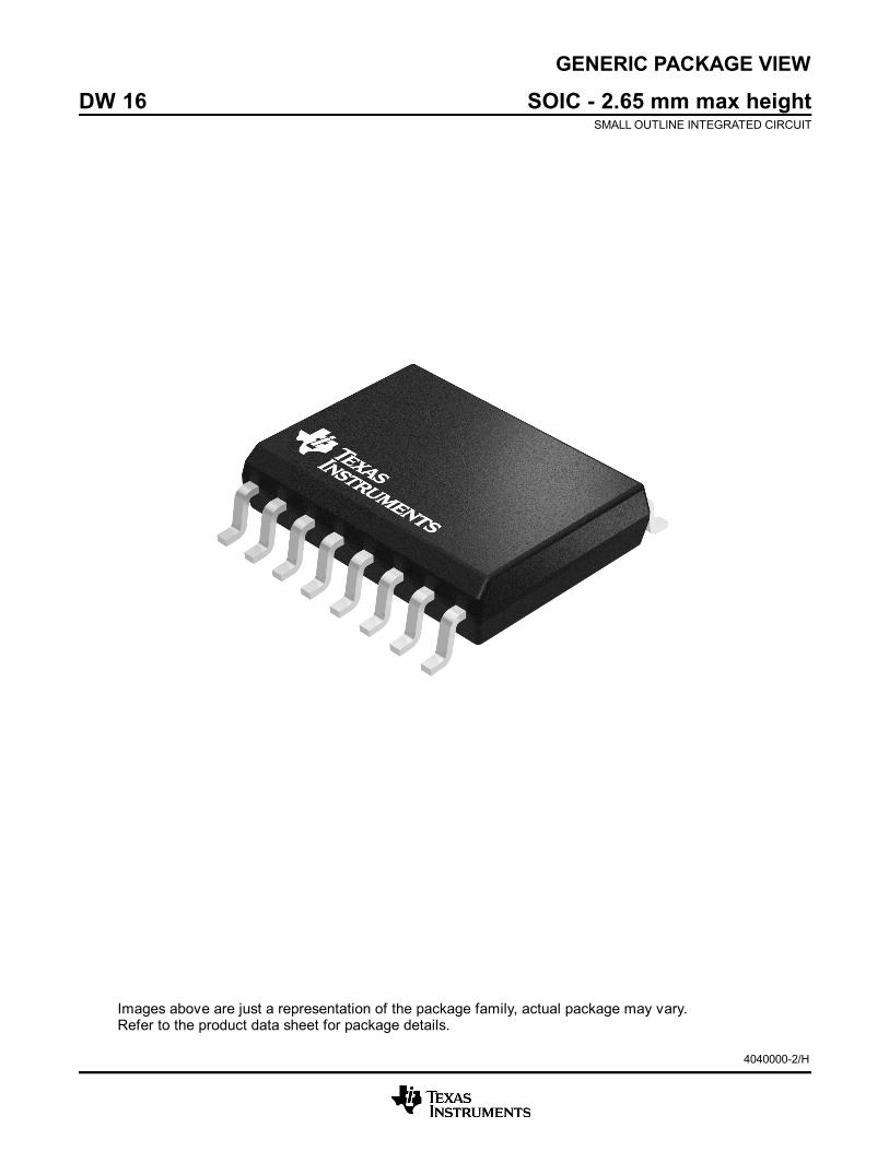
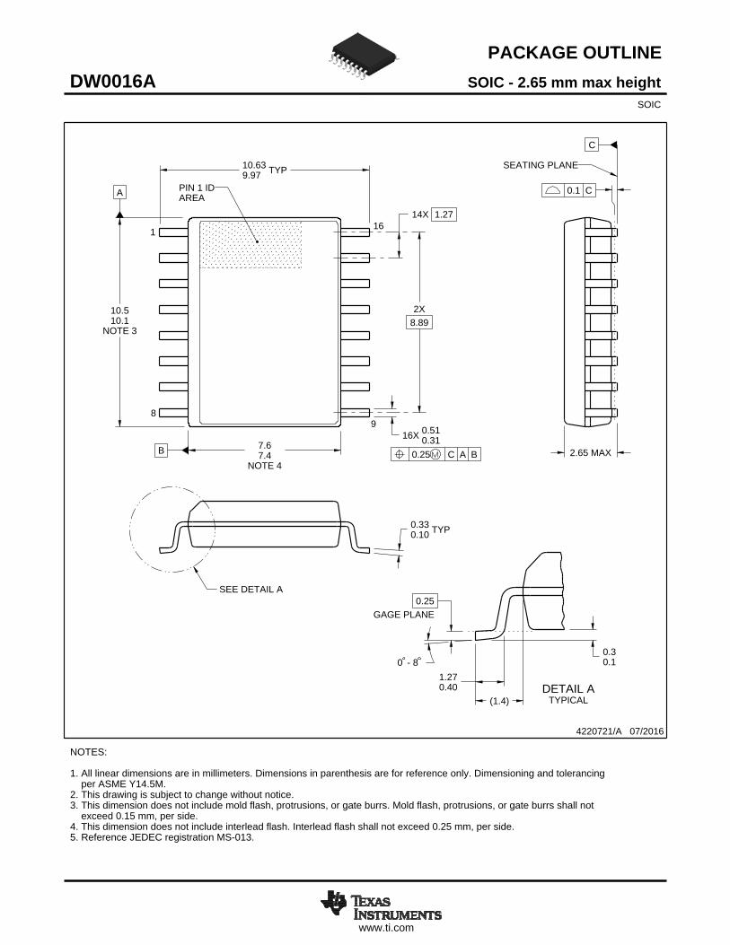
GENERIC PACKAGE VIEW
Images above are just a representation of the package family, actual package may vary.Refer to the product data sheet for package details.
DW 16 SOIC - 2.65 mm max heightSMALL OUTLINE INTEGRATED CIRCUIT
4040000-2/H
www.ti.com
PACKAGE OUTLINE
C
TYP10.639.97
2.65 MAX
14X 1.27
16X 0.510.31
2X8.89
TYP0.330.10
0 - 80.30.1
(1.4)
0.25GAGE PLANE
1.270.40
A
NOTE 3
10.510.1
BNOTE 4
7.67.4
4220721/A 07/2016
SOIC - 2.65 mm max heightDW0016ASOIC
NOTES: 1. All linear dimensions are in millimeters. Dimensions in parenthesis are for reference only. Dimensioning and tolerancing per ASME Y14.5M. 2. This drawing is subject to change without notice. 3. This dimension does not include mold flash, protrusions, or gate burrs. Mold flash, protrusions, or gate burrs shall not exceed 0.15 mm, per side. 4. This dimension does not include interlead flash. Interlead flash shall not exceed 0.25 mm, per side.5. Reference JEDEC registration MS-013.
1 16
0.25 C A B
98
PIN 1 IDAREA
SEATING PLANE
0.1 C
SEE DETAIL A
DETAIL ATYPICAL
SCALE 1.500
www.ti.com
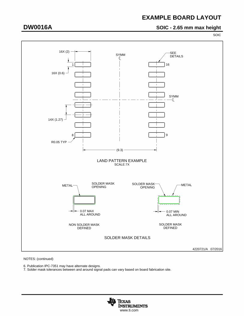
EXAMPLE BOARD LAYOUT
0.07 MAXALL AROUND
0.07 MINALL AROUND
(9.3)
14X (1.27)
R0.05 TYP
16X (2)
16X (0.6)
4220721/A 07/2016
SOIC - 2.65 mm max heightDW0016ASOIC
NOTES: (continued) 6. Publication IPC-7351 may have alternate designs. 7. Solder mask tolerances between and around signal pads can vary based on board fabrication site.
METAL SOLDER MASKOPENING
NON SOLDER MASKDEFINED
SOLDER MASK DETAILS
OPENINGSOLDER MASK METAL
SOLDER MASKDEFINED
LAND PATTERN EXAMPLESCALE:7X
SYMM
1
8 9
16
SEEDETAILS
SYMM
www.ti.com
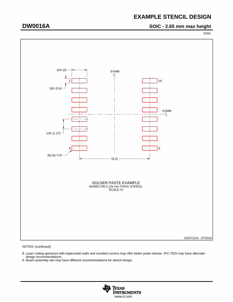
EXAMPLE STENCIL DESIGN
R0.05 TYP
16X (2)
16X (0.6)
14X (1.27)
(9.3)
4220721/A 07/2016
SOIC - 2.65 mm max heightDW0016ASOIC
NOTES: (continued) 8. Laser cutting apertures with trapezoidal walls and rounded corners may offer better paste release. IPC-7525 may have alternate design recommendations. 9. Board assembly site may have different recommendations for stencil design.
SOLDER PASTE EXAMPLEBASED ON 0.125 mm THICK STENCIL
SCALE:7X
SYMM
SYMM
1
8 9
16
IMPORTANT NOTICE
Texas Instruments Incorporated (TI) reserves the right to make corrections, enhancements, improvements and other changes to itssemiconductor products and services per JESD46, latest issue, and to discontinue any product or service per JESD48, latest issue. Buyersshould obtain the latest relevant information before placing orders and should verify that such information is current and complete.TI’s published terms of sale for semiconductor products (http://www.ti.com/sc/docs/stdterms.htm) apply to the sale of packaged integratedcircuit products that TI has qualified and released to market. Additional terms may apply to the use or sale of other types of TI products andservices.Reproduction of significant portions of TI information in TI data sheets is permissible only if reproduction is without alteration and isaccompanied by all associated warranties, conditions, limitations, and notices. TI is not responsible or liable for such reproduceddocumentation. Information of third parties may be subject to additional restrictions. Resale of TI products or services with statementsdifferent from or beyond the parameters stated by TI for that product or service voids all express and any implied warranties for theassociated TI product or service and is an unfair and deceptive business practice. TI is not responsible or liable for any such statements.Buyers and others who are developing systems that incorporate TI products (collectively, “Designers”) understand and agree that Designersremain responsible for using their independent analysis, evaluation and judgment in designing their applications and that Designers havefull and exclusive responsibility to assure the safety of Designers' applications and compliance of their applications (and of all TI productsused in or for Designers’ applications) with all applicable regulations, laws and other applicable requirements. Designer represents that, withrespect to their applications, Designer has all the necessary expertise to create and implement safeguards that (1) anticipate dangerousconsequences of failures, (2) monitor failures and their consequences, and (3) lessen the likelihood of failures that might cause harm andtake appropriate actions. Designer agrees that prior to using or distributing any applications that include TI products, Designer willthoroughly test such applications and the functionality of such TI products as used in such applications.TI’s provision of technical, application or other design advice, quality characterization, reliability data or other services or information,including, but not limited to, reference designs and materials relating to evaluation modules, (collectively, “TI Resources”) are intended toassist designers who are developing applications that incorporate TI products; by downloading, accessing or using TI Resources in anyway, Designer (individually or, if Designer is acting on behalf of a company, Designer’s company) agrees to use any particular TI Resourcesolely for this purpose and subject to the terms of this Notice.TI’s provision of TI Resources does not expand or otherwise alter TI’s applicable published warranties or warranty disclaimers for TIproducts, and no additional obligations or liabilities arise from TI providing such TI Resources. TI reserves the right to make corrections,enhancements, improvements and other changes to its TI Resources. TI has not conducted any testing other than that specificallydescribed in the published documentation for a particular TI Resource.Designer is authorized to use, copy and modify any individual TI Resource only in connection with the development of applications thatinclude the TI product(s) identified in such TI Resource. NO OTHER LICENSE, EXPRESS OR IMPLIED, BY ESTOPPEL OR OTHERWISETO ANY OTHER TI INTELLECTUAL PROPERTY RIGHT, AND NO LICENSE TO ANY TECHNOLOGY OR INTELLECTUAL PROPERTYRIGHT OF TI OR ANY THIRD PARTY IS GRANTED HEREIN, including but not limited to any patent right, copyright, mask work right, orother intellectual property right relating to any combination, machine, or process in which TI products or services are used. Informationregarding or referencing third-party products or services does not constitute a license to use such products or services, or a warranty orendorsement thereof. Use of TI Resources may require a license from a third party under the patents or other intellectual property of thethird party, or a license from TI under the patents or other intellectual property of TI.TI RESOURCES ARE PROVIDED “AS IS” AND WITH ALL FAULTS. TI DISCLAIMS ALL OTHER WARRANTIES ORREPRESENTATIONS, EXPRESS OR IMPLIED, REGARDING RESOURCES OR USE THEREOF, INCLUDING BUT NOT LIMITED TOACCURACY OR COMPLETENESS, TITLE, ANY EPIDEMIC FAILURE WARRANTY AND ANY IMPLIED WARRANTIES OFMERCHANTABILITY, FITNESS FOR A PARTICULAR PURPOSE, AND NON-INFRINGEMENT OF ANY THIRD PARTY INTELLECTUALPROPERTY RIGHTS. TI SHALL NOT BE LIABLE FOR AND SHALL NOT DEFEND OR INDEMNIFY DESIGNER AGAINST ANY CLAIM,INCLUDING BUT NOT LIMITED TO ANY INFRINGEMENT CLAIM THAT RELATES TO OR IS BASED ON ANY COMBINATION OFPRODUCTS EVEN IF DESCRIBED IN TI RESOURCES OR OTHERWISE. IN NO EVENT SHALL TI BE LIABLE FOR ANY ACTUAL,DIRECT, SPECIAL, COLLATERAL, INDIRECT, PUNITIVE, INCIDENTAL, CONSEQUENTIAL OR EXEMPLARY DAMAGES INCONNECTION WITH OR ARISING OUT OF TI RESOURCES OR USE THEREOF, AND REGARDLESS OF WHETHER TI HAS BEENADVISED OF THE POSSIBILITY OF SUCH DAMAGES.Unless TI has explicitly designated an individual product as meeting the requirements of a particular industry standard (e.g., ISO/TS 16949and ISO 26262), TI is not responsible for any failure to meet such industry standard requirements.Where TI specifically promotes products as facilitating functional safety or as compliant with industry functional safety standards, suchproducts are intended to help enable customers to design and create their own applications that meet applicable functional safety standardsand requirements. Using products in an application does not by itself establish any safety features in the application. Designers mustensure compliance with safety-related requirements and standards applicable to their applications. Designer may not use any TI products inlife-critical medical equipment unless authorized officers of the parties have executed a special contract specifically governing such use.Life-critical medical equipment is medical equipment where failure of such equipment would cause serious bodily injury or death (e.g., lifesupport, pacemakers, defibrillators, heart pumps, neurostimulators, and implantables). Such equipment includes, without limitation, allmedical devices identified by the U.S. Food and Drug Administration as Class III devices and equivalent classifications outside the U.S.TI may expressly designate certain products as completing a particular qualification (e.g., Q100, Military Grade, or Enhanced Product).Designers agree that it has the necessary expertise to select the product with the appropriate qualification designation for their applicationsand that proper product selection is at Designers’ own risk. Designers are solely responsible for compliance with all legal and regulatoryrequirements in connection with such selection.Designer will fully indemnify TI and its representatives against any damages, costs, losses, and/or liabilities arising out of Designer’s non-compliance with the terms and provisions of this Notice.
Mailing Address: Texas Instruments, Post Office Box 655303, Dallas, Texas 75265Copyright © 2018, Texas Instruments Incorporated
Mouser Electronics
Authorized Distributor
Click to View Pricing, Inventory, Delivery & Lifecycle Information: Texas Instruments:
LOG112AID LOG112AIDE4 LOG112AIDR