sbs 1.1-compliantgas gauge enabled with impedance … sheets/texas... · 2016-03-02 · www .ti.com...
TRANSCRIPT

www.ti.com
FEATURES APPLICATIONS
DESCRIPTION
bq20z70-V110
SLUS742–OCTOBER 2006–REVISED OCTOBER 2006
SBS 1.1-COMPLIANT GAS GAUGE ENABLED WITH IMPEDANCE TRACK™TECHNOLOGY FOR USE WITH THE bq29330
• Notebook PCs• Next Generation Patented Impedance Track™Technology accurately Measures Available • Medical and Test EquipmentCharge in Li-Ion and Li-Polymer Batteries • Portable Instrumentation
• Better than 1% Error Over Lifetime of theBattery
• Instant Accuracy – No Learning Cycle The bq20z70-V110 SBS-compliant gas gauge IC,Required incorporating patented Impedance Track™
technology, is designed for battery-pack or in-system• Supports the Smart Battery Specificationinstallation. The bq20z70-V110 measures andSBS V1.1maintains an accurate record of available charge in
• Powerful 8-Bit RISC CPU With Ultra-Low Li-ion or Li-polymer batteries using its integratedPower Modes high-performance analog peripherals. The
bq20z70-V110 monitors capacity change, battery• Works With the TI bq29330 Analog Front-Endimpedance, open-circuit voltage, and other critical(AFE) Protection IC to Provide Complete Packparameters of the battery pack, and reports theElectronics Solutioninformation to the system host controller over a• Full Array of Programmable Protection serial-communication bus. It is designed to work with
Features the bq29330 analog front-end (AFE) protection IC to– Voltage, Current and Temperature maximize functionality and safety, and minimize
component count and cost in smart battery circuits.• Fully Integrated High Accurate Clock• Flexible Configuration for 2 to 4 Series Li-Ion The Impedance Track technology continuously
analyzes the battery impedance, resulting in superiorand Li-Polymer Cellsgas-gauging accuracy. This enables remaining• Integrated Field Programmable FLASHcapacity to be calculated with discharge rate,Memory Eliminates the Need for Externaltemperature, and cell aging all accounted for during
Configuration Memory each stage of every cycle.• Smart Battery Charger Control Feature
AVAILABLE OPTIONS• Two 16-Bit Delta-Sigma ConverterPACKAGE– Accurate Voltage and Temperature
TAMeasurements 20-PIN TSSOP (PW) 20-PIN TSSOP (PW)Tube Tape & Reel– Integrating Coloumb Counter for Charge
–40°C toFlow bq20z70-V110PW (1) bq20z70-V110PWR (2)85°C
• Better Than 0.65 nVh of Resolution• Self-Calibrating
• Supports SHA-1 Authentication(1) A single tube quantity is 50 units.
• 20-Pin TSSOP (PW) (2) A single reel quantity is 2000 units
Please be aware that an important notice concerning availability, standard warranty, and use in critical applications of TexasInstruments semiconductor products and disclaimers thereto appears at the end of this data sheet.
IMPEDANCE TRACK is a trademark of Texas Instruments.
PRODUCTION DATA information is current as of publication date. Copyright © 2006, Texas Instruments IncorporatedProducts conform to specifications per the terms of the TexasInstruments standard warranty. Production processing does notnecessarily include testing of all parameters.

www.ti.com
SYSTEM PARTITIONING DIAGRAM
Charge Pumps
Overcurrent &Short Circuit
Protection
Cell
Se
lection
Multip
lexer
N-CH FETDrive
ImpedanceTrack™ Gas
Gauging
Cell
Ba
lancin
gD
rive
2n
dL
evelV
olta
ge
Pro
tection
Pack -
SMBus
Pack +
LDO& Therm. Drive
& Reset
Therm
Fuse
TemperatureMeasurement
& Protection
32kHz Clock
Generator
System
Interface
Voltage LevelTranslator
Watchdog &Protection
Timing
System
Interface
SHA-1Authentication
Charging
Algorithm
SBS v1.1
Data
Cell & Pack
VoltageMeasurement
OverrcurrentProtection
Overvoltage &
UndervoltageProtection
Cell BalancingAlgorithm &
Control
Fail SafeProtection
bq29330
Validation &
Control
bq20z70-V110 bq29330 bq294xy
Supply Voltage
32KHz
I2C
Registers
Alert
RSNS5mΩ – 20mΩ typ.
Reset
1XALERT
2TS2
3TS1
4CLKOUT
5
6PFIN
7SAFE
8SMBD
9NC
10SMBC
VCELL-20
VCELL+19
VCC18
VSS17
MRST16
SRN15
SRP14
VSS13
SCLK12
SDATA11
PRES
bq20z70-V110
SLUS742–OCTOBER 2006–REVISED OCTOBER 2006
TSSOP (PW)(TOP VIEW)
2 Submit Documentation Feedback

www.ti.com
ABSOLUTE MAXIMUM RATINGS
ELECTRICAL CHARACTERISTICS
bq20z70-V110
SLUS742–OCTOBER 2006–REVISED OCTOBER 2006
TERMINAL FUNCTIONS
TERMINALI/O (1) DESCRIPTION
NO. NAME
1 XALERT I Alert interrupt input from bq29330. Connect directly to bq29330 XALERT pin
2 TS2 I 2nd thermistor voltage input connection to monitor temperature
3 TS1 I 1st thermistor voltage input connection to monitor temperature
4 CLKOUT O 32.768kHz output for bq29330 watchdog. Connect directly to bq29330 WDI pin
5 PRES I Active low input to sense system insertion
6 PFIN I Active low input to sense secondary protector output status
7 SAFE O Active high output to enforce additional level of safety, e.g. fuse blow
8 SMBD I/OD SMBus data open drain bidirectional pin used for communication with bq20z70-V110
9 NC – Not used - leave floating
10 SMBC I/OD SMBus clock open drain bidirectional pin used for communication with bq20z70-V110
11 SDATA I/OD Data transfer line from and to bq29330. Connect directly to SDATA pin of bq29330
12 SCLK I/OD Data clock line to bq29330. Connect directly to SCLK pin of bq29330
13 VSS I/OD VSS
14 SRP IA Connection for a small-value resistor to monitor the battery charge and discharge current flow
15 SRN IA Connection for a small-value resistor to monitor the battery charge and discharge current flow
Master reset input that forces the device into reset when held low. Connect directly to XRST pin of16 MRST I bq29330
17 VSS P Negative supply. Both VSS needs to be connected together
18 VCC P Positive supply
19 VCELL+ I Positive differential cell input. Connect directly to CELL+ pin of bq29330
20 VCELL- I Negative differential cell input. Connect directly to CELL- pin of bq29330
(1) I = Input, IA = Analog input, I/O = Input/output, I/OD = Input/Open-drain output, O = Output, OA = Analog output, P = Power
over operating free-air temperature range (unless otherwise noted) (1)
RANGE
VCC relative to VSS(2) Supply voltage range on VCC pin –0.3 V to 2.75 V
V(IOD) relative to VSS(2) XALERT, PFIN, SAFE, SMBD, SMBC, SDATA, SCLK, –0.3 V to 6.0 V
VI relative to VSS(2) TS2, TS1, CLKOUT, PRES, SRP, SRN, MRST, VCELL+,VCELL- –0.3 V to VCC + 0.3 V
TA Operating free-air temperature range –40°C to 85°C
Tstg Storage temperature range –65°C to 150°C
(1) Stresses beyond those listed under absolute maximum ratings may cause permanent damage to the device. These are stress ratingsonly, and functional operation of the device at these or any other conditions beyond those indicated under recommended operatingconditions is not implied. Exposure to absolute-maximum-rated conditions for extended periods may affect device reliability.
(2) VSS refers to Voltage at VSS pin.
VCC = 2.4 V to 2.6 V, TA = -40°C - 85°C (unless otherwise noted)
PARAMETER TEST CONDITIONS MIN TYP MAX UNIT
VDD Supply voltage VDDA and VDDD 2.4 2.5 2.6 V
No flash programming 400 (1)
IDD Operating mode current µAbq20z70-V110 + 475bq29330
Sleep mode 8 (1)
I(SLP) Low-power storage mode current µAbq20z70-V110 + 48bq29330
(1) This value does not include the bq29330
3Submit Documentation Feedback

www.ti.com
bq20z70-V110
SLUS742–OCTOBER 2006–REVISED OCTOBER 2006
ELECTRICAL CHARACTERISTICS (continued)VCC = 2.4 V to 2.6 V, TA = -40°C - 85°C (unless otherwise noted)
PARAMETER TEST CONDITIONS MIN TYP MAX UNIT
Shutdown Mode 0.1 (1)
I(SLP) Shutdown Current µAbq20z70-V110 + 0.2bq29330
Output voltage low CLKOUT, SAFE, SMBD, SMBC, SDATA, IOL = 7 mA 0.4VOL VSCLK
VOH Output high voltage CLKOUT, SAFE, SMBD,SMBC, SDATA, IOH = –0.5 mA VCC– 0.5 VSCLK
VIL Input voltage low PRES, PFIN, SMBD, SMBC, SDATA, MRST 0.8 V
VIH Input voltage high PRES, PFIN, SMBD, SMBC, SDATA, MRST 2.0 V
CIN Input capacitance 5 pF
V(AI1) Input voltage range TS1, TS2, VCELL+, VCELL- – 0.2 0.8 x VCCV
V(AI2) Input voltage range SRP, SRN – 0.2 0.2
Z(AI1) Input impedance TS1, TS2, VCELL+, VCELL - 0 V – 1 V 8 MΩ
Z(AI2) Input impedance SRP, SRN 0 V – 1 V 2.5 MΩ
4 Submit Documentation Feedback

www.ti.com
POWER-ON RESET
1.76
1.77
1.78
1.79
1.8
1.81
-40 -20 0 20 40 60 80
T - Free-Air Temperature - °CA
Po
we
r-O
n R
es
et
Ne
ga
tiv
e-G
oin
g V
olt
ag
e -
V
INTEGRATING ADC (Coulomb Counter) CHARACTERISTICS
OSCILLATOR
bq20z70-V110
SLUS742–OCTOBER 2006–REVISED OCTOBER 2006
VCC = 2.4 V to 2.6 V, TA = –40°C to 85°C (unless otherwise noted)
PARAMETER TEST CONDITIONS MIN TYP MAX UNIT
VIT– Negative-going voltage input 1.7 1.8 1.9 V
VHYS Power-on reset hysteresis 50 125 200 mV
VCC = 2.4 V to 2.6 V, TA = –40°C to 85°C (unless otherwise noted)
PARAMETER TEST CONDITIONS MIN TYP MAX UNIT
V(SR) Input voltage range, V(SRN) and V(SRP) V(SR) = V(SRP) – V(SRN) –0.20 0.20 V
V(SROS) Input offset TA =25°C to 85°C 10 µV
INL Integral nonlinearity error ±0.007 ±0.037 %
VCC = 2.4 V to 2.6 V, TA = –40°C to 85°C (unless otherwise noted)
PARAMETER TEST CONDITIONS MIN TYP MAX UNIT
HIGH FREQUENCY OSCILLATOR
f (OSC) Operating frequency 4.194 MHz
-3% 0.25% 3%f (EIO) Frequency error (1) (2)
T A = 20°C to 70°C -2% 0.25% 2%
f (sxo) Start-up time (3) 2.5 5 ms
LOW FREQUENCY OSCILLATOR
f (LOSC) Operating frequency 32.768 kHz
f (LEIO) -2.5% 0.25% 2.5%Frequency error (2) (4)
T A = 20°C to 70°C -1.5% 0.25% 1.5%
f (Lsxo) Start-up time (5) 500 µs
(1) The frequency error is measured from 4.194 MHz.(2) The frequency drift is included and measured f rom the trimmed frequency at V CC = 2.5 V, T A = 25°C.(3) The start-up time is defined as the time it takes for the oscillator output frequency to be within 1% of the specified frequency.(4) The frequency error is measured from 32.768 kHz.(5) The start-up time is defined as the time it takes for the oscillator output frequency to be ±3%.
5Submit Documentation Feedback
www.ti.com
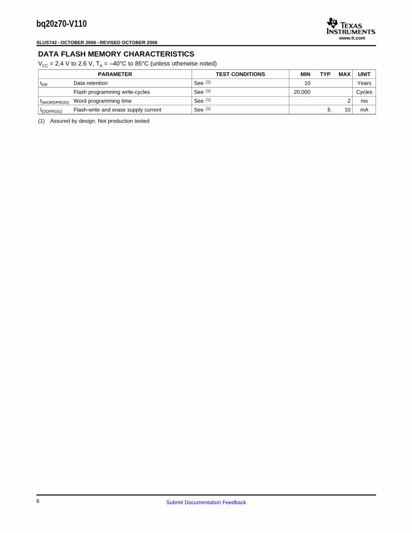
DATA FLASH MEMORY CHARACTERISTICS
bq20z70-V110
SLUS742–OCTOBER 2006–REVISED OCTOBER 2006
VCC = 2.4 V to 2.6 V, TA = –40°C to 85°C (unless otherwise noted)
PARAMETER TEST CONDITIONS MIN TYP MAX UNIT
tDR Data retention See (1) 10 Years
Flash programming write-cycles See (1) 20,000 Cycles
t(WORDPROG) Word programming time See (1) 2 ms
I(DDPROG) Flash-write and erase supply current See (1) 5 10 mA
(1) Assured by design. Not production tested
6 Submit Documentation Feedback

www.ti.com
SMBus TIMING SPECIFICATIONS
bq20z70-V110
SLUS742–OCTOBER 2006–REVISED OCTOBER 2006
VCC = 2.4 V to 2.6 V, TA = –40°C to 85°C (unless otherwise noted)
PARAMETER TEST CONDITIONS MIN TYP MAX UNIT
fSMB SMBus operating frequency Slave mode, SMBC 50% duty cycle 10 100kHz
fMAS SMBus master clock frequency Master mode, no clock low slave extend 51.2
tBUF Bus free time between start and stop 4.7
tHD:STA Hold time after (repeated) start 4µs
tSU:STA Repeated start setup time 4.7
tSU:STO Stop setup time 4
Receive mode 0tHD:DAT Data hold time
Transmit mode 300 ns
tSU:DAT Data setup time 250
tTIMEOUT Error signal/detect See (1) 25 35 ms
tLOW Clock low period 4.7µs
tHIGH Clock high period See (2) 4 50
tLOW:SEXT Cumulative clock low slave extend time See (3) 25ms
tLOW:MEXT Cumulative clock low master extend time See (4) 10
tF Clock/data fall time (VILMAX– 0.15 V) to (VIHMIN + 0.15 V) 300ns
tR Clock/data rise time 0.9 VCC to (VILMAX – 0.15 V) 1000
(1) The bq20z70-V110 times out when any clock low exceeds tTIMEOUT.(2) tHIGH:MAX. is minimum bus idle time. SMBC = 1 for t > 50 µs causes reset of any transaction involving the bq20z70-V110 that is in
progress.(3) tLOW:SEXT is the cumulative time a slave device is allowed to extend the clock cycles in one message from initial start to the stop.(4) tLOW:MEXT is the cumulative time a master device is allowed to extend the clock cycles in one message from initial start to the stop.
SMBus TIMING DIAGRAM
7Submit Documentation Feedback

www.ti.com
FEATURE SET
Primary (1st Level) Safety Features
Secondary (2nd Level) Safety Features
Charge Control Features
Gas Gauging
Authentication
Power Modes
bq20z70-V110
SLUS742–OCTOBER 2006–REVISED OCTOBER 2006
The bq20z70-V110 supports a wide range of battery and system protection features that can easily beconfigured. The primary safety features include:
• Cell over/under voltage protection• Charge and Discharge over current• Short Circut• Charge and Discharge Over temperature• AFE Watchdog
The secondary safety features of the bq20z70-V110 can be used to indicate more serious faults via the SAFE(pin 7). This pin can be used to blow an in-line fuse to permanently disable the battery pack from charging ordischarging. The secondary safety protection features include:
• Safety over voltage• Safety over current in Charge and Discharge• Safety over temperature in Charge and Discharge• Charge FET and 0 Volt Charge FET fault• Discharge FET fault• AFE communication fault
The bq20z70-V110 charge control features include:
• Reports the appropriate charging current needed for constant current charging and the appropriate chargingvoltage needed for constant voltage charging to a smart charger using SMBus broadcasts.
• Determines the chemical state of charge of each battery cell using Impedance Track™ and can reduce thecharge difference of the battery cells in fully charged state of the battery pack gradually using cell balancingalgorithm during charging. This prevents fully charged cells from overcharging and causing excessivedegradation and also increases the usable pack energy by preventing premature charge termination
• Supports pre-charging/zero-volt charging• Support fast charging• Supports charge inhibit and charge suspend if battery pack temperature is out of temperature range• Reports charging fault and also indicate charge status via charge and discharge alarms.
The bq20z70-V110 uses the Impedance Track™ Technology to measure and calculate the available charge inbattery cells. The achievable accuracy is better than 1% error over the lifetime of the battery and there is no fullcharge discharge learning cycle required.
See Theory and Implementation of Impedance Track Battery Fuel-Gauging Algorithm application note(SLUA364) for further details.
The bq20z70-V110 supports authentication by the host using SHA-1.
The bq20z70-V110 supports 3 different power modes to reduce power consumption:
• In Normal Mode, the bq20z70-V110 performs measurements, calculations, protection decisions and dataupdates in 1 second intervals. Between these intervals, the bq20z70-V110 is in a reduced power stage.
8 Submit Documentation Feedback

www.ti.com
CONFIGURATION
Oscillator Function
System Present Operation
BATTERY PARAMETER MEASUREMENTS
Charge and Discharge Counting
Voltage
Current
Auto Calibration
Temperature
bq20z70-V110
SLUS742–OCTOBER 2006–REVISED OCTOBER 2006
FEATURE SET (continued)
• In Sleep Mode, the bq20z70-V110 performs measurements, calculations, protection decisions and dataupdate in adjustable time intervals. Between these intervals, the bq20z70-V110 is in a reduced power stage.The bq20z70-V110 has a wake function that enables exit from Sleep mode, when current flow or failure isdetected.
• In Shutdown Mode the bq20z70-V110 is completely disabled.
The bq20z70-V110 fully integrates the system oscillators. Therefore the bq20z70-V110 requires no externalcomponents for this feature.
The bq20z70-V110 pulls the PU pin high periodically (1 s). Connect this pin to the PRES pin of thebq20z70-V110 via a resistor of approximately 5 kΩ. The bq20z70-V110 measures the PRES input during thePU-active period to determine its state. If PRES input is pulled to ground by external system, the bq20z70-V110detects this as system present.
The bq20z70-V110 uses an integrating delta-sigma analog-to-digital converter (ADC) for current measurement,and a second delta-sigma ADC for individual cell and battery voltage, and temperature measurement.
The integrating delta-sigma ADC measures the charge/discharge flow of the battery by measuring the voltagedrop across a small-value sense resistor between the SR1 and SR2 pins. The integrating ADC measures bipolarsignals from -0.25 V to 0.25 V. The bq20z70-V110 detects charge activity when VSR = V(SR1)-V(SR2)is positiveand discharge activity when VSR = V(SR1)-V(SR2) is negative. The bq20z70-V110 continuously integrates thesignal over time, using an internal counter. The fundamental rate of the counter is 0.65 nVh.
The bq20z70-V110 updates the individual series cell voltages through the bq29330 at one second intervals. Thebq20z70-V110 configures the bq29330 to connect the selected cell, cell offset, or bq29330 VREF to the CELLpin of the bq29330, which is required to be connected to VIN of the bq20z70-V110. The internal ADC of thebq20z70-V110 measures the voltage, scales and calibrates it appropriately. This data is also used to calculatethe impedance of the cell for the Impedance Track™ gas-gauging.
The bq20z70-V110 uses the SRP and SRN inputs to measure and calculate the battery charge and dischargecurrent using a 5 mΩ to 20 mΩ typ. sense resistor.
The bq20z70-V110 provides an auto-calibration feature to cancel the voltage offset error across SRN and SRPfor maximum charge measurement accuracy. The bq20z70-V110 performs auto-calibration when the SMBuslines stay low continuously for a minimum of 5 s.
The bq20z70-V110 has an internal temperature sensor and 2 external temperature sensor inputs TS1 and TS2used in conjunction with two identical NTC thermistors (default are Semitec 103AT) to sense the batteryenviromental temperature. The bq20z70-V110 can be configured to use internal or external temperaturesensors.
9Submit Documentation Feedback

www.ti.com
COMMUNICATIONS
SMBus On and Off State
bq20z70-V110
SLUS742–OCTOBER 2006–REVISED OCTOBER 2006
FEATURE SET (continued)
The bq20z70-V110 uses SMBus v1.1 with Master Mode and package error checking (PEC) options per the SBSspecification.
The bq20z70-V110 detects an SMBus off state when SMBC and SMBD are logic-low for ≥ 2 seconds. Clearingthis state requires either SMBC or SMBD to transition high. Within 1 ms, the communication bus is available.
10 Submit Documentation Feedback

www.ti.com
SBS and Dataflash Values
bq20z70-V110
SLUS742–OCTOBER 2006–REVISED OCTOBER 2006
FEATURE SET (continued)
Table 1. SBS COMMANDS
SBS Mode Name Format Size in Min Max Default UnitCmd Bytes Value Value Value
0x00 R/W ManufacturerAccess hex 2 0x0000 0xffff —
0x01 R/W RemainingCapacityAlarm unsigned int 2 0 65535 — mAh or10mWh
0x02 R/W RemainingTimeAlarm unsigned int 2 0 65535 — min
0x03 R/W BatteryMode hex 2 0x0000 0xffff —
0x04 R/W AtRate signed int 2 -32768 32767 — mA or 10mW
0x05 R AtRateTimeToFull unsigned int 2 0 65535 — min
0x06 R AtRateTimeToEmpty unsigned int 2 0 65535 — min
0x07 R AtRateOK unsigned int 2 0 65535 —
0x08 R Temperature unsigned int 2 0 65535 — 0.1°K
0x09 R Voltage unsigned int 2 0 20000 — mV
0x0a R Current signed int 2 -32768 32767 — mA
0x0b R AverageCurrent signed int 2 -32768 32767 — mA
0x0c R MaxError unsigned int 1 0 100 — %
0x0d R RelativeStateOfCharge unsigned int 1 0 100 — %
0x0e R AbsoluteStateOfCharge unsigned int 1 0 100 — %
0x0f R/W RemainingCapacity unsigned int 2 0 65535 — mAh or10mWh
0x10 R FullChargeCapacity unsigned int 2 0 65535 — mAh or10mWh
0x11 R RunTimeToEmpty unsigned int 2 0 65535 — min
0x12 R AverageTimeToEmpty unsigned int 2 0 65535 — min
0x13 R AverageTimeToFull unsigned int 2 0 65535 — min
0x14 R ChargingCurrent unsigned int 2 0 65535 — mA
0x15 R ChargingVoltage unsigned int 2 0 65535 — mV
0x16 R BatteryStatus unsigned int 2 0x0000 0xffff —
0x17 R/W CycleCount unsigned int 2 0 65535 —
0x18 R/W DesignCapacity unsigned int 2 0 65535 — mAh or10mWh
0x19 R/W DesignVoltage unsigned int 2 7000 16000 14400 mV
0x1a R/W SpecificationInfo unsigned int 2 0x0000 0xffff 0x0031
0x1b R/W ManufactureDate unsigned int 2 0 65535 0
0x1c R/W SerialNumber hex 2 0x0000 0xffff 0x0001
0x20 R/W ManufacturerName String 11+1 — — Texas ASCIIInstruments
0x21 R/W DeviceName String 7+1 — — bq20z70- ASCIIV110
0x22 R/W DeviceChemistry String 4+1 — — LION ASCII
0x23 R ManufacturerData String 14+1 — — — ASCII
0x2f R/W Authenticate String 20+1 — — — ASCII
0x3c R CellVoltage4 unsigned int 2 0 65535 — mV
0x3d R CellVoltage3 unsigned int 2 0 65535 — mV
0x3e R CellVoltage2 unsigned int 2 0 65535 — mV
0x3f R CellVoltage1 unsigned int 2 0 65535 — mV
11Submit Documentation Feedback

www.ti.com
bq20z70-V110
SLUS742–OCTOBER 2006–REVISED OCTOBER 2006
Table 2. EXTENDED SBS COMMANDS
SBS Mode Name Format Size in Min Value Max Value Default UnitCmd Bytes Value
0x45 R AFEData String 11+1 — — — ASCII
0x46 R/W FETControl hex 1 0x00 0xff —
0x4f R StateOfHealth unsigned int 1 0 100 — %
0x51 R SafetyStatus hex 2 0x0000 0xffff —
0x53 R PFStatus hex 2 0x0000 0xffff —
0x54 R OperationStatus hex 2 0x0000 0xffff —
0x55 R ChargingStatus hex 2 0x0000 0xffff —
0x57 R ResetData hex 2 0x0000 0xffff —
0x5a R PackVoltage unsigned int 2 0 65535 — mV
0x5d R AverageVoltage unsigned int 2 0 65535 — mV
0x60 R/W UnSealKey hex 4 0x00000000 0xffffffff —
0x61 R/W FullAccessKey hex 4 0x00000000 0xffffffff —
0x62 R/W PFKey hex 4 0x00000000 0xffffffff —
0x63 R/W AuthenKey3 hex 4 0x00000000 0xffffffff —
0x64 R/W AuthenKey2 hex 4 0x00000000 0xffffffff —
0x65 R/W AuthenKey1 hex 4 0x00000000 0xffffffff —
0x66 R/W AuthenKey0 hex 4 0x00000000 0xffffffff —
0x70 R/W ManufacturerInfo String 8+1 — — —
0x71 R/W SenseResistor unsigned int 2 0 65535 — µΩ
0x77 R/W DataFlashSubClassID hex 2 0x0000 0xffff —
0x78 R/W DataFlashSubClassPage1 hex 32 — — —
0x79 R/W DataFlashSubClassPage2 hex 32 — — —
0x7a R/W DataFlashSubClassPage3 hex 32 — — —
0x7b R/W DataFlashSubClassPage4 hex 32 — — —
0x7c R/W DataFlashSubClassPage5 hex 32 — — —
0x7d R/W DataFlashSubClassPage6 hex 32 — — —
0x7e R/W DataFlashSubClassPage7 hex 32 — — —
0x7f R/W DataFlashSubClassPage8 hex 32 — — —
NOTE:
All reserved bits in Data Flash should be written to zero.
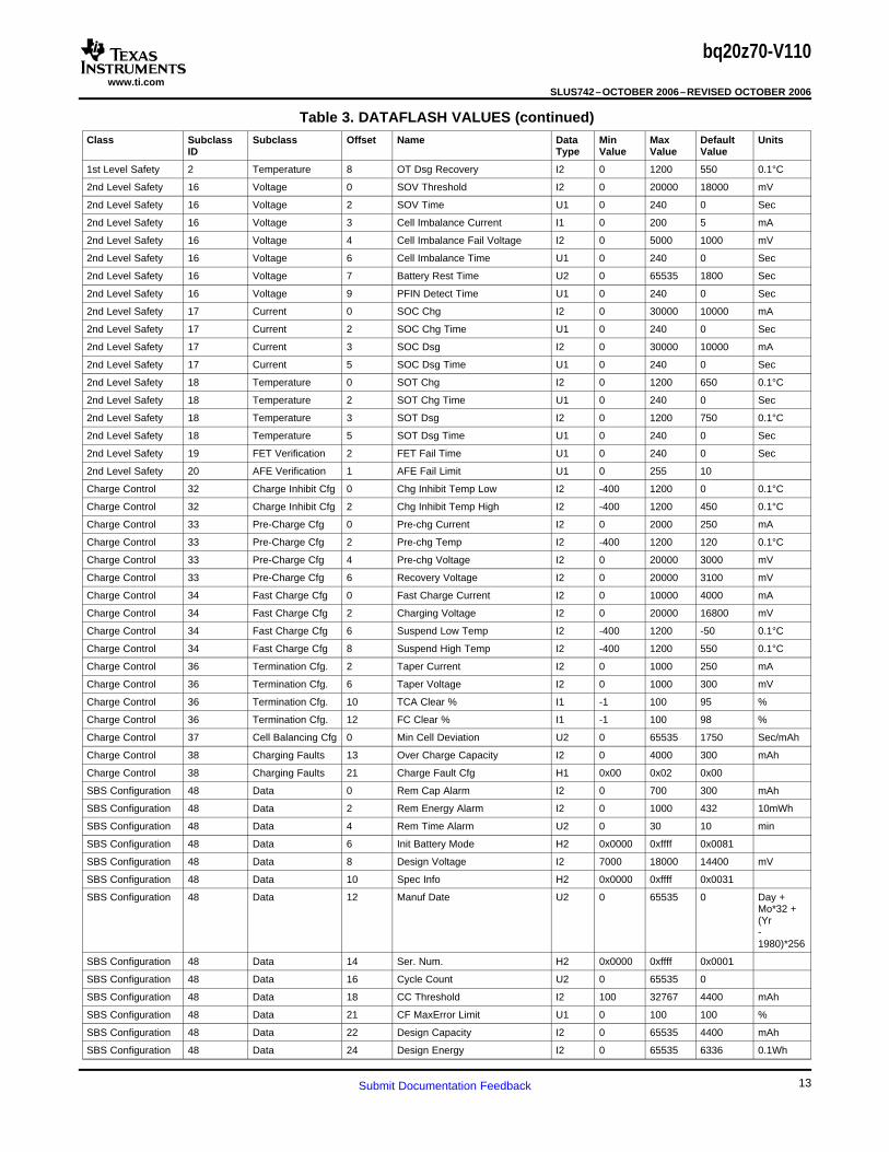
Table 3. DATAFLASH VALUESClass Subclass Subclass Offset Name Data Min Max Default Units
ID Type Value Value Value
1st Level Safety 0 Voltage 0 COV Threshold I2 3700 5000 4300 mV
1st Level Safety 0 Voltage 3 COV Recovery I2 0 4400 3900 mV
1st Level Safety 0 Voltage 12 CUV Threshold I2 0 3500 2200 mV
1st Level Safety 0 Voltage 15 CUV Recovery I2 0 3600 3000 mV
1st Level Safety 1 Current 0 OC (1st Tier) Chg I2 0 20000 6000 mA
1st Level Safety 1 Current 5 OC (1st Tier) Dsg I2 0 20000 6000 mA
1st Level Safety 1 Current 16 Current Recovery Time U1 0 240 8 Sec
1st Level Safety 1 Current 17 AFE OC Dsg H1 0x00 0x1f 0x12
1st Level Safety 1 Current 18 AFE OC Dsg Time H1 0x00 0xff 0x0f
1st Level Safety 1 Current 21 AFE SC Chg Cfg H1 0x00 0xff 0x77
1st Level Safety 1 Current 22 AFE SC Dsg Cfg H1 0x00 0xff 0x77
1st Level Safety 2 Temperature 0 Over Temp Chg I2 0 1200 550 0.1°C
1st Level Safety 2 Temperature 3 OT Chg Recovery I2 0 1200 500 0.1°C
1st Level Safety 2 Temperature 5 Over Temp Dsg I2 0 1200 600 0.1°C
12 Submit Documentation Feedback
www.ti.com
bq20z70-V110
SLUS742–OCTOBER 2006–REVISED OCTOBER 2006
Table 3. DATAFLASH VALUES (continued)Class Subclass Subclass Offset Name Data Min Max Default Units
ID Type Value Value Value
1st Level Safety 2 Temperature 8 OT Dsg Recovery I2 0 1200 550 0.1°C
2nd Level Safety 16 Voltage 0 SOV Threshold I2 0 20000 18000 mV
2nd Level Safety 16 Voltage 2 SOV Time U1 0 240 0 Sec
2nd Level Safety 16 Voltage 3 Cell Imbalance Current I1 0 200 5 mA
2nd Level Safety 16 Voltage 4 Cell Imbalance Fail Voltage I2 0 5000 1000 mV
2nd Level Safety 16 Voltage 6 Cell Imbalance Time U1 0 240 0 Sec
2nd Level Safety 16 Voltage 7 Battery Rest Time U2 0 65535 1800 Sec
2nd Level Safety 16 Voltage 9 PFIN Detect Time U1 0 240 0 Sec
2nd Level Safety 17 Current 0 SOC Chg I2 0 30000 10000 mA
2nd Level Safety 17 Current 2 SOC Chg Time U1 0 240 0 Sec
2nd Level Safety 17 Current 3 SOC Dsg I2 0 30000 10000 mA
2nd Level Safety 17 Current 5 SOC Dsg Time U1 0 240 0 Sec
2nd Level Safety 18 Temperature 0 SOT Chg I2 0 1200 650 0.1°C
2nd Level Safety 18 Temperature 2 SOT Chg Time U1 0 240 0 Sec
2nd Level Safety 18 Temperature 3 SOT Dsg I2 0 1200 750 0.1°C
2nd Level Safety 18 Temperature 5 SOT Dsg Time U1 0 240 0 Sec
2nd Level Safety 19 FET Verification 2 FET Fail Time U1 0 240 0 Sec
2nd Level Safety 20 AFE Verification 1 AFE Fail Limit U1 0 255 10
Charge Control 32 Charge Inhibit Cfg 0 Chg Inhibit Temp Low I2 -400 1200 0 0.1°C
Charge Control 32 Charge Inhibit Cfg 2 Chg Inhibit Temp High I2 -400 1200 450 0.1°C
Charge Control 33 Pre-Charge Cfg 0 Pre-chg Current I2 0 2000 250 mA
Charge Control 33 Pre-Charge Cfg 2 Pre-chg Temp I2 -400 1200 120 0.1°C
Charge Control 33 Pre-Charge Cfg 4 Pre-chg Voltage I2 0 20000 3000 mV
Charge Control 33 Pre-Charge Cfg 6 Recovery Voltage I2 0 20000 3100 mV
Charge Control 34 Fast Charge Cfg 0 Fast Charge Current I2 0 10000 4000 mA
Charge Control 34 Fast Charge Cfg 2 Charging Voltage I2 0 20000 16800 mV
Charge Control 34 Fast Charge Cfg 6 Suspend Low Temp I2 -400 1200 -50 0.1°C
Charge Control 34 Fast Charge Cfg 8 Suspend High Temp I2 -400 1200 550 0.1°C
Charge Control 36 Termination Cfg. 2 Taper Current I2 0 1000 250 mA
Charge Control 36 Termination Cfg. 6 Taper Voltage I2 0 1000 300 mV
Charge Control 36 Termination Cfg. 10 TCA Clear % I1 -1 100 95 %
Charge Control 36 Termination Cfg. 12 FC Clear % I1 -1 100 98 %
Charge Control 37 Cell Balancing Cfg 0 Min Cell Deviation U2 0 65535 1750 Sec/mAh
Charge Control 38 Charging Faults 13 Over Charge Capacity I2 0 4000 300 mAh
Charge Control 38 Charging Faults 21 Charge Fault Cfg H1 0x00 0x02 0x00
SBS Configuration 48 Data 0 Rem Cap Alarm I2 0 700 300 mAh
SBS Configuration 48 Data 2 Rem Energy Alarm I2 0 1000 432 10mWh
SBS Configuration 48 Data 4 Rem Time Alarm U2 0 30 10 min
SBS Configuration 48 Data 6 Init Battery Mode H2 0x0000 0xffff 0x0081
SBS Configuration 48 Data 8 Design Voltage I2 7000 18000 14400 mV
SBS Configuration 48 Data 10 Spec Info H2 0x0000 0xffff 0x0031
SBS Configuration 48 Data 12 Manuf Date U2 0 65535 0 Day +Mo*32 +(Yr-1980)*256
SBS Configuration 48 Data 14 Ser. Num. H2 0x0000 0xffff 0x0001
SBS Configuration 48 Data 16 Cycle Count U2 0 65535 0
SBS Configuration 48 Data 18 CC Threshold I2 100 32767 4400 mAh
SBS Configuration 48 Data 21 CF MaxError Limit U1 0 100 100 %
SBS Configuration 48 Data 22 Design Capacity I2 0 65535 4400 mAh
SBS Configuration 48 Data 24 Design Energy I2 0 65535 6336 0.1Wh
13Submit Documentation Feedback

www.ti.com
bq20z70-V110
SLUS742–OCTOBER 2006–REVISED OCTOBER 2006
Table 3. DATAFLASH VALUES (continued)Class Subclass Subclass Offset Name Data Min Max Default Units
ID Type Value Value Value
SBS Configuration 48 Data 26 Manuf Name S12 - - Texas ASCIIInst.
SBS Configuration 48 Data 38 Device Name S8 - - bq20z70- ASCIIV110
SBS Configuration 48 Data 46 Device Chemistry S5 - - LION ASCII
SBS Configuration 49 Configuration 0 TDA Set % I1 -1 100 6 %
SBS Configuration 49 Configuration 1 TDA Clear % I1 -1 100 8 %
SBS Configuration 49 Configuration 2 FD Set % I1 -1 100 2 %
SBS Configuration 49 Configuration 3 FD Clear % I1 -1 100 5 %
SBS Configuration 49 Configuration 4 TDA Set Volt Threshold I2 0 16800 5000 mV
SBS Configuration 49 Configuration 6 TDA Set Volt Time U1 0 240 0 Sec
SBS Configuration 49 Configuration 7 TDA Clear Volt I2 0 16800 5500 mV
System Data 58 Manufacturer Info 0 Manuf. Info S9 01234567 ASCII89abcdef0123
Configuration 64 Registers 0 Operation Cfg A H2 0x0000 0x033b 0x033b
Configuration 64 Registers 2 Operation Cfg B H2 0x0000 0x3eff 0x2440
Configuration 64 Registers 4 Operation Cfg C H2 0x0000 0x0001 0x0000
Configuration 64 Registers 6 Permanent Fail Cfg H2 0x0000 0x4dff 0x0000
Configuration 64 Registers 8 Non-Removable Cfg H2 0x0000 0x3027 0x0000
Power 68 Power 0 Flash Update OK Voltage I2 6000 20000 7500 mV
Power 68 Power 2 Shutdown Voltage I2 5000 20000 7000 mV
Power 68 Power 5 Charger Present I2 0 23000 3000 mV
Power 68 Power 16 Wake Current Reg H1 0x00 0xff 0x00
Gas Gauging 80 IT Cfg 0 Load Select U1 0 255 3
Gas Gauging 80 IT Cfg 1 Load Mode U1 0 255 0
Gas Gauging 80 IT Cfg 45 Term Voltage I2 -32768 32767 12000 mV
Gas Gauging 80 IT Cfg 60 User Rate-mA I2 -9000 -2000 0 mA
Gas Gauging 80 IT Cfg 62 User Rate-mW I2 -14000 -3000 0 0.1W
Gas Gauging 80 IT Cfg 64 Reserve Cap-mAh I2 0 9000 0 mAh
Gas Gauging 80 IT Cfg 66 Reserve Cap-mWh I2 0 14000 0 0.1Wh
Gas Gauging 81 Current 0 Dsg Current Threshold I2 0 2000 50 mAThresholds
Gas Gauging 81 Current 2 Chg Current Threshold I2 0 2000 25 mAThresholds
Gas Gauging 81 Current 4 Quit Current I2 0 1000 10 mAThresholds
Gas Gauging 82 State 0 Qmax Cell0 I2 0 65535 4400 mAh
Gas Gauging 82 State 2 Qmax Cell1 I2 0 65535 4400 mAh
Gas Gauging 82 State 4 Qmax Cell2 I2 0 65535 4400 mAh
Gas Gauging 82 State 6 Qmax Cell3 I2 0 65535 4400 mAh
Gas Gauging 82 State 8 Qmax Pack I2 0 65535 4400 mAh
Gas Gauging 82 State 12 Update Status H1 0x00 0x03 0x00
Gas Gauging 82 State 25 Delta Voltage I2 -32768 32767 0 mV
Ra Table 88 R_a0 0 Cell0 R_a flag H2 0x0000 0xffff 0xff55
Ra Table 88 R_a0 2 Cell0 R_a 0 I2 0 32767 160 2^-10ohm
Ra Table 88 R_a0 4 Cell0 R_a 1 I2 0 32767 166 2^-10ohm
Ra Table 88 R_a0 6 Cell0 R_a 2 I2 0 32767 153 2^-10ohm
Ra Table 88 R_a0 8 Cell0 R_a 3 I2 0 32767 151 2^-10ohm
Ra Table 88 R_a0 10 Cell0 R_a 4 I2 0 32767 145 2^-10ohm
Ra Table 88 R_a0 12 Cell0 R_a 5 I2 0 32767 152 2^-10ohm
Ra Table 88 R_a0 14 Cell0 R_a 6 I2 0 32767 176 2^-10ohm
Ra Table 88 R_a0 16 Cell0 R_a 7 I2 0 32767 204 2^-10ohm
14 Submit Documentation Feedback

www.ti.com
bq20z70-V110
SLUS742–OCTOBER 2006–REVISED OCTOBER 2006
Table 3. DATAFLASH VALUES (continued)Class Subclass Subclass Offset Name Data Min Max Default Units
ID Type Value Value Value
Ra Table 88 R_a0 18 Cell0 R_a 8 I2 0 32767 222 2^-10ohm
Ra Table 88 R_a0 20 Cell0 R_a 9 I2 0 32767 254 2^-10ohm
Ra Table 88 R_a0 22 Cell0 R_a 10 I2 0 32767 315 2^-10ohm
Ra Table 88 R_a0 24 Cell0 R_a 11 I2 0 32767 437 2^-10ohm
Ra Table 88 R_a0 26 Cell0 R_a 12 I2 0 32767 651 2^-10ohm
Ra Table 88 R_a0 28 Cell0 R_a 13 I2 0 32767 1001 2^-10ohm
Ra Table 88 R_a0 30 Cell0 R_a 14 I2 0 32767 1458 2^-10ohm
Ra Table 89 R_a1 0 Cell1 R_a flag H2 0x0000 0xffff 0xff55
Ra Table 89 R_a1 2 Cell1 R_a 0 I2 0 32767 160 2^-10ohm
Ra Table 89 R_a1 4 Cell1 R_a 1 I2 0 32767 166 2^-10ohm
Ra Table 89 R_a1 6 Cell1 R_a 2 I2 0 32767 153 2^-10ohm
Ra Table 89 R_a1 8 Cell1 R_a 3 I2 0 32767 151 2^-10ohm
Ra Table 89 R_a1 10 Cell1 R_a 4 I2 0 32767 145 2^-10ohm
Ra Table 89 R_a1 12 Cell1 R_a 5 I2 0 32767 152 2^-10ohm
Ra Table 89 R_a1 14 Cell1 R_a 6 I2 0 32767 176 2^-10ohm
Ra Table 89 R_a1 16 Cell1 R_a 7 I2 0 32767 204 2^-10ohm
Ra Table 89 R_a1 18 Cell1 R_a 8 I2 0 32767 222 2^-10ohm
Ra Table 89 R_a1 20 Cell1 R_a 9 I2 0 32767 254 2^-10ohm
Ra Table 89 R_a1 22 Cell1 R_a 10 I2 0 32767 315 2^-10ohm
Ra Table 89 R_a1 24 Cell1 R_a 11 I2 0 32767 437 2^-10ohm
Ra Table 89 R_a1 26 Cell1 R_a 12 I2 0 32767 651 2^-10ohm
Ra Table 89 R_a1 28 Cell1 R_a 13 I2 0 32767 1001 2^-10ohm
Ra Table 89 R_a1 30 Cell1 R_a 14 I2 0 32767 1458 2^-10ohm
Ra Table 90 R_a2 0 Cell2 R_a flag H2 0x0000 0xffff 0xff55
Ra Table 90 R_a2 2 Cell2 R_a 0 I2 0 32767 160 2^-10ohm
Ra Table 90 R_a2 4 Cell2 R_a 1 I2 0 32767 166 2^-10ohm
Ra Table 90 R_a2 6 Cell2 R_a 2 I2 0 32767 153 2^-10ohm
Ra Table 90 R_a2 8 Cell2 R_a 3 I2 0 32767 151 2^-10ohm
Ra Table 90 R_a2 10 Cell2 R_a 4 I2 0 32767 145 2^-10ohm
Ra Table 90 R_a2 12 Cell2 R_a 5 I2 0 32767 152 2^-10ohm
Ra Table 90 R_a2 14 Cell2 R_a 6 I2 0 32767 176 2^-10ohm
Ra Table 90 R_a2 16 Cell2 R_a 7 I2 0 32767 204 2^-10ohm
Ra Table 90 R_a2 18 Cell2 R_a 8 I2 0 32767 222 2^-10ohm
Ra Table 90 R_a2 20 Cell2 R_a 9 I2 0 32767 254 2^-10ohm
Ra Table 90 R_a2 22 Cell2 R_a 10 I2 0 32767 315 2^-10ohm
Ra Table 90 R_a2 24 Cell2 R_a 11 I2 0 32767 437 2^-10ohm
Ra Table 90 R_a2 26 Cell2 R_a 12 I2 0 32767 651 2^-10ohm
Ra Table 90 R_a2 28 Cell2 R_a 13 I2 0 32767 1001 2^-10ohm
Ra Table 90 R_a2 30 Cell2 R_a 14 I2 0 32767 1458 2^-10ohm
Ra Table 91 R_a3 0 Cell3 R_a flag H2 0x0000 0xffff 0xff55
Ra Table 91 R_a3 2 Cell3 R_a 0 I2 0 32767 160 2^-10ohm
Ra Table 91 R_a3 4 Cell3 R_a 1 I2 0 32767 166 2^-10ohm
Ra Table 91 R_a3 6 Cell3 R_a 2 I2 0 32767 153 2^-10ohm
Ra Table 91 R_a3 8 Cell3 R_a 3 I2 0 32767 151 2^-10ohm
Ra Table 91 R_a3 10 Cell3 R_a 4 I2 0 32767 145 2^-10ohm
Ra Table 91 R_a3 12 Cell3 R_a 5 I2 0 32767 152 2^-10ohm
Ra Table 91 R_a3 14 Cell3 R_a 6 I2 0 32767 176 2^-10ohm
Ra Table 91 R_a3 16 Cell3 R_a 7 I2 0 32767 204 2^-10ohm
Ra Table 91 R_a3 18 Cell3 R_a 8 I2 0 32767 222 2^-10ohm
Ra Table 91 R_a3 20 Cell3 R_a 9 I2 0 32767 254 2^-10ohm
15Submit Documentation Feedback

www.ti.com
bq20z70-V110
SLUS742–OCTOBER 2006–REVISED OCTOBER 2006
Table 3. DATAFLASH VALUES (continued)Class Subclass Subclass Offset Name Data Min Max Default Units
ID Type Value Value Value
Ra Table 91 R_a3 22 Cell3 R_a 10 I2 0 32767 315 2^-10ohm
Ra Table 91 R_a3 24 Cell3 R_a 11 I2 0 32767 437 2^-10ohm
Ra Table 91 R_a3 26 Cell3 R_a 12 I2 0 32767 651 2^-10ohm
Ra Table 91 R_a3 28 Cell3 R_a 13 I2 0 32767 1001 2^-10ohm
Ra Table 91 R_a3 30 Cell3 R_a 14 I2 0 32767 1458 2^-10ohm
Ra Table 92 R_a0x 0 xCell0 R_a flag H2 0x0000 0xffff 0xffff
Ra Table 92 R_a0x 2 xCell0 R_a 0 I2 0 32767 160 2^-10ohm
Ra Table 92 R_a0x 4 xCell0 R_a 1 I2 0 32767 166 2^-10ohm
Ra Table 92 R_a0x 6 xCell0 R_a 2 I2 0 32767 153 2^-10ohm
Ra Table 92 R_a0x 8 xCell0 R_a 3 I2 0 32767 151 2^-10ohm
Ra Table 92 R_a0x 10 xCell0 R_a 4 I2 0 32767 145 2^-10ohm
Ra Table 92 R_a0x 12 xCell0 R_a 5 I2 0 32767 152 2^-10ohm
Ra Table 92 R_a0x 14 xCell0 R_a 6 I2 0 32767 176 2^-10ohm
Ra Table 92 R_a0x 16 xCell0 R_a 7 I2 0 32767 204 2^-10ohm
Ra Table 92 R_a0x 18 xCell0 R_a 8 I2 0 32767 222 2^-10ohm
Ra Table 92 R_a0x 20 xCell0 R_a 9 I2 0 32767 254 2^-10ohm
Ra Table 92 R_a0x 22 xCell0 R_a 10 I2 0 32767 315 2^-10ohm
Ra Table 92 R_a0x 24 xCell0 R_a 11 I2 0 32767 437 2^-10ohm
Ra Table 92 R_a0x 26 xCell0 R_a 12 I2 0 32767 651 2^-10ohm
Ra Table 92 R_a0x 28 xCell0 R_a 13 I2 0 32767 1001 2^-10ohm
Ra Table 92 R_a0x 30 xCell0 R_a 14 I2 0 32767 1458 2^-10ohm
Ra Table 93 R_a1x 0 xCell1 R_a flag H2 0x0000 0xffff 0xffff
Ra Table 93 R_a1x 2 xCell1 R_a 0 I2 0 32767 160 2^-10ohm
Ra Table 93 R_a1x 4 xCell1 R_a 1 I2 0 32767 166 2^-10ohm
Ra Table 93 R_a1x 6 xCell1 R_a 2 I2 0 32767 153 2^-10ohm
Ra Table 93 R_a1x 8 xCell1 R_a 3 I2 0 32767 151 2^-10ohm
Ra Table 93 R_a1x 10 xCell1 R_a 4 I2 0 32767 145 2^-10ohm
Ra Table 93 R_a1x 12 xCell1 R_a 5 I2 0 32767 152 2^-10ohm
Ra Table 93 R_a1x 14 xCell1 R_a 6 I2 0 32767 176 2^-10ohm
Ra Table 93 R_a1x 16 xCell1 R_a 7 I2 0 32767 204 2^-10ohm
Ra Table 93 R_a1x 18 xCell1 R_a 8 I2 0 32767 222 2^-10ohm
Ra Table 93 R_a1x 20 xCell1 R_a 9 I2 0 32767 254 2^-10ohm
Ra Table 93 R_a1x 22 xCell1 R_a 10 I2 0 32767 315 2^-10ohm
Ra Table 93 R_a1x 24 xCell1 R_a 11 I2 0 32767 437 2^-10ohm
Ra Table 93 R_a1x 26 xCell1 R_a 12 I2 0 32767 651 2^-10ohm
Ra Table 93 R_a1x 28 xCell1 R_a 13 I2 0 32767 1001 2^-10ohm
Ra Table 93 R_a1x 30 xCell1 R_a 14 I2 0 32767 1458 2^-10ohm
Ra Table 94 R_a2x 0 xCell2 R_a flag H2 0x0000 0xffff 0xffff
Ra Table 94 R_a2x 2 xCell2 R_a 0 I2 0 32767 160 2^-10ohm
Ra Table 94 R_a2x 4 xCell2 R_a 1 I2 0 32767 166 2^-10ohm
Ra Table 94 R_a2x 6 xCell2 R_a 2 I2 0 32767 153 2^-10ohm
Ra Table 94 R_a2x 8 xCell2 R_a 3 I2 0 32767 151 2^-10ohm
Ra Table 94 R_a2x 10 xCell2 R_a 4 I2 0 32767 145 2^-10ohm
Ra Table 94 R_a2x 12 xCell2 R_a 5 I2 0 32767 152 2^-10ohm
Ra Table 94 R_a2x 14 xCell2 R_a 6 I2 0 32767 176 2^-10ohm
Ra Table 94 R_a2x 16 xCell2 R_a 7 I2 0 32767 204 2^-10ohm
Ra Table 94 R_a2x 18 xCell2 R_a 8 I2 0 32767 222 2^-10ohm
Ra Table 94 R_a2x 20 xCell2 R_a 9 I2 0 32767 254 2^-10ohm
Ra Table 94 R_a2x 22 xCell2 R_a 10 I2 0 32767 315 2^-10ohm
Ra Table 94 R_a2x 24 xCell2 R_a 11 I2 0 32767 437 2^-10ohm
16 Submit Documentation Feedback

www.ti.com
bq20z70-V110
SLUS742–OCTOBER 2006–REVISED OCTOBER 2006
Table 3. DATAFLASH VALUES (continued)Class Subclass Subclass Offset Name Data Min Max Default Units
ID Type Value Value Value
Ra Table 94 R_a2x 26 xCell2 R_a 12 I2 0 32767 651 2^-10ohm
Ra Table 94 R_a2x 28 xCell2 R_a 13 I2 0 32767 1001 2^-10ohm
Ra Table 94 R_a2x 30 xCell2 R_a 14 I2 0 32767 1458 2^-10ohm
Ra Table 95 R_a3x 0 xCell3 R_a flag H2 0x0000 0xffff 0xffff
Ra Table 95 R_a3x 2 xCell3 R_a 0 I2 0 32767 160 2^-10ohm
Ra Table 95 R_a3x 4 xCell3 R_a 1 I2 0 32767 166 2^-10ohm
Ra Table 95 R_a3x 6 xCell3 R_a 2 I2 0 32767 153 2^-10ohm
Ra Table 95 R_a3x 8 xCell3 R_a 3 I2 0 32767 151 2^-10ohm
Ra Table 95 R_a3x 10 xCell3 R_a 4 I2 0 32767 145 2^-10ohm
Ra Table 95 R_a3x 12 xCell3 R_a 5 I2 0 32767 152 2^-10ohm
Ra Table 95 R_a3x 14 xCell3 R_a 6 I2 0 32767 176 2^-10ohm
Ra Table 95 R_a3x 16 xCell3 R_a 7 I2 0 32767 204 2^-10ohm
Ra Table 95 R_a3x 18 xCell3 R_a 8 I2 0 32767 222 2^-10ohm
Ra Table 95 R_a3x 20 xCell3 R_a 9 I2 0 32767 254 2^-10ohm
Ra Table 95 R_a3x 22 xCell3 R_a 10 I2 0 32767 315 2^-10ohm
Ra Table 95 R_a3x 24 xCell3 R_a 11 I2 0 32767 437 2^-10ohm
Ra Table 95 R_a3x 26 xCell3 R_a 12 I2 0 32767 651 2^-10ohm
Ra Table 95 R_a3x 28 xCell3 R_a 13 I2 0 32767 1001 2^-10ohm
Ra Table 95 R_a3x 30 xCell3 R_a 14 I2 0 32767 1458 2^-10ohm
PF Status 96 Device Status 0 PF Flags 1 H2 0x0000 0x4dff 0x0000Data
PF Status 96 Device Status 28 PF Flags 2 H2 0x0000 0x0dff 0x0000Data
Calibration 104 Data 0 CC Gain F4 0.1 4 0.9419
Calibration 104 Data 4 CC Delta F4 29826 1193046 280932.625
Calibration 104 Data 8 Ref Voltage I2 0 65536 24500 50uV
Calibration 104 Data 12 AFE Pack Gain I2 0 65536 22050 µV/cnt
Calibration 104 Data 14 CC Offset I2 -32768 32767 -1667
Calibration 104 Data 16 Board Offset I2 -32768 32767 0
Calibration 104 Data 18 Int Temp Offset I1 -128 127 0
Calibration 104 Data 19 Ext1 Temp Offset I1 -128 127 0
Calibration 104 Data 20 Ext2 Temp Offset I1 -128 127 0
Calibration 105 Config 0 CC Current I2 0 65535 3000 mA
Calibration 105 Config 2 Voltage Signal I2 0 65535 16800 mV
Calibration 105 Config 4 Temp Signal I2 0 65535 2980 0.1K
Calibration 105 Config 6 CC Offset Time U2 0 65535 250 mSec
Calibration 105 Config 8 ADC Offset Time U2 0 65535 32 mSec
Calibration 105 Config 10 CC Gain Time U2 0 65535 250 mSec
Calibration 105 Config 12 Voltage Time U2 0 65535 1984 mSec
Calibration 105 Config 14 Temperature Time U2 0 65535 32 mSec
Calibration 105 Config 17 Cal Mode Timeout U2 0 65535 38400 Sec/128
Calibration 106 Temp Model 0 Ext Coef 1 I2 -32768 32767 -28285 Sec
Calibration 106 Temp Model 2 Ext Coef 2 I2 -32768 32767 20848 Sec
Calibration 106 Temp Model 4 Ext Coef 3 I2 -32768 32767 -7537 Sec
Calibration 106 Temp Model 6 Ext Coef 4 I2 -32768 32767 4012 Sec
Calibration 106 Temp Model 8 Ext Min AD I2 -32768 32767 0 Sec
Calibration 106 Temp Model 10 Ext Max Temp I2 -32768 32767 4012 Sec
Calibration 106 Temp Model 12 Int Coef 1 I2 -32768 32767 0 Sec
Calibration 106 Temp Model 14 Int Coef 2 I2 -32768 32767 0 Sec
Calibration 106 Temp Model 16 Int Coef 3 I2 -32768 32767 -11136 Sec
17Submit Documentation Feedback

www.ti.com
Application Schematic
bq20z70-V110
SLUS742–OCTOBER 2006–REVISED OCTOBER 2006
Table 3. DATAFLASH VALUES (continued)Class Subclass Subclass Offset Name Data Min Max Default Units
ID Type Value Value Value
Calibration 106 Temp Model 18 Int Coef 4 I2 -32768 32767 5754 Sec
Calibration 106 Temp Model 20 Int Min AD I2 -32768 32767 0 Sec
Calibration 106 Temp Model 22 Int Max Temp I2 -32768 32767 5754 Sec
Calibration 107 Current 0 Filter U1 0 255 239
Calibration 107 Current 1 Deadband U1 0 255 3 mA
Calibration 107 Current 2 CC Deadband U1 0 255 34 294 nV
The application schematic is on the following page.
18 Submit Documentation Feedback

PACKAGE OPTION ADDENDUM
www.ti.com 31-Aug-2014
Addendum-Page 1
PACKAGING INFORMATION
Orderable Device Status(1)
Package Type PackageDrawing
Pins PackageQty
Eco Plan(2)
Lead/Ball Finish(6)
MSL Peak Temp(3)
Op Temp (°C) Device Marking(4/5)
Samples
BQ20Z70PWR-V110 OBSOLETE TSSOP PW 20 TBD Call TI Call TI -40 to 85 20Z70PW (1) The marketing status values are defined as follows:ACTIVE: Product device recommended for new designs.LIFEBUY: TI has announced that the device will be discontinued, and a lifetime-buy period is in effect.NRND: Not recommended for new designs. Device is in production to support existing customers, but TI does not recommend using this part in a new design.PREVIEW: Device has been announced but is not in production. Samples may or may not be available.OBSOLETE: TI has discontinued the production of the device.
(2) Eco Plan - The planned eco-friendly classification: Pb-Free (RoHS), Pb-Free (RoHS Exempt), or Green (RoHS & no Sb/Br) - please check http://www.ti.com/productcontent for the latest availabilityinformation and additional product content details.TBD: The Pb-Free/Green conversion plan has not been defined.Pb-Free (RoHS): TI's terms "Lead-Free" or "Pb-Free" mean semiconductor products that are compatible with the current RoHS requirements for all 6 substances, including the requirement thatlead not exceed 0.1% by weight in homogeneous materials. Where designed to be soldered at high temperatures, TI Pb-Free products are suitable for use in specified lead-free processes.Pb-Free (RoHS Exempt): This component has a RoHS exemption for either 1) lead-based flip-chip solder bumps used between the die and package, or 2) lead-based die adhesive used betweenthe die and leadframe. The component is otherwise considered Pb-Free (RoHS compatible) as defined above.Green (RoHS & no Sb/Br): TI defines "Green" to mean Pb-Free (RoHS compatible), and free of Bromine (Br) and Antimony (Sb) based flame retardants (Br or Sb do not exceed 0.1% by weightin homogeneous material)
(3) MSL, Peak Temp. - The Moisture Sensitivity Level rating according to the JEDEC industry standard classifications, and peak solder temperature.
(4) There may be additional marking, which relates to the logo, the lot trace code information, or the environmental category on the device.
(5) Multiple Device Markings will be inside parentheses. Only one Device Marking contained in parentheses and separated by a "~" will appear on a device. If a line is indented then it is a continuationof the previous line and the two combined represent the entire Device Marking for that device.
(6) Lead/Ball Finish - Orderable Devices may have multiple material finish options. Finish options are separated by a vertical ruled line. Lead/Ball Finish values may wrap to two lines if the finishvalue exceeds the maximum column width.
Important Information and Disclaimer:The information provided on this page represents TI's knowledge and belief as of the date that it is provided. TI bases its knowledge and belief on informationprovided by third parties, and makes no representation or warranty as to the accuracy of such information. Efforts are underway to better integrate information from third parties. TI has taken andcontinues to take reasonable steps to provide representative and accurate information but may not have conducted destructive testing or chemical analysis on incoming materials and chemicals.TI and TI suppliers consider certain information to be proprietary, and thus CAS numbers and other limited information may not be available for release.
In no event shall TI's liability arising out of such information exceed the total purchase price of the TI part(s) at issue in this document sold by TI to Customer on an annual basis.


IMPORTANT NOTICETexas Instruments Incorporated and its subsidiaries (TI) reserve the right to make corrections, enhancements, improvements and otherchanges to its semiconductor products and services per JESD46, latest issue, and to discontinue any product or service per JESD48, latestissue. Buyers should obtain the latest relevant information before placing orders and should verify that such information is current andcomplete. All semiconductor products (also referred to herein as “components”) are sold subject to TI’s terms and conditions of salesupplied at the time of order acknowledgment.TI warrants performance of its components to the specifications applicable at the time of sale, in accordance with the warranty in TI’s termsand conditions of sale of semiconductor products. Testing and other quality control techniques are used to the extent TI deems necessaryto support this warranty. Except where mandated by applicable law, testing of all parameters of each component is not necessarilyperformed.TI assumes no liability for applications assistance or the design of Buyers’ products. Buyers are responsible for their products andapplications using TI components. To minimize the risks associated with Buyers’ products and applications, Buyers should provideadequate design and operating safeguards.TI does not warrant or represent that any license, either express or implied, is granted under any patent right, copyright, mask work right, orother intellectual property right relating to any combination, machine, or process in which TI components or services are used. Informationpublished by TI regarding third-party products or services does not constitute a license to use such products or services or a warranty orendorsement thereof. Use of such information may require a license from a third party under the patents or other intellectual property of thethird party, or a license from TI under the patents or other intellectual property of TI.Reproduction of significant portions of TI information in TI data books or data sheets is permissible only if reproduction is without alterationand is accompanied by all associated warranties, conditions, limitations, and notices. TI is not responsible or liable for such altereddocumentation. Information of third parties may be subject to additional restrictions.Resale of TI components or services with statements different from or beyond the parameters stated by TI for that component or servicevoids all express and any implied warranties for the associated TI component or service and is an unfair and deceptive business practice.TI is not responsible or liable for any such statements.Buyer acknowledges and agrees that it is solely responsible for compliance with all legal, regulatory and safety-related requirementsconcerning its products, and any use of TI components in its applications, notwithstanding any applications-related information or supportthat may be provided by TI. Buyer represents and agrees that it has all the necessary expertise to create and implement safeguards whichanticipate dangerous consequences of failures, monitor failures and their consequences, lessen the likelihood of failures that might causeharm and take appropriate remedial actions. Buyer will fully indemnify TI and its representatives against any damages arising out of the useof any TI components in safety-critical applications.In some cases, TI components may be promoted specifically to facilitate safety-related applications. With such components, TI’s goal is tohelp enable customers to design and create their own end-product solutions that meet applicable functional safety standards andrequirements. Nonetheless, such components are subject to these terms.No TI components are authorized for use in FDA Class III (or similar life-critical medical equipment) unless authorized officers of the partieshave executed a special agreement specifically governing such use.Only those TI components which TI has specifically designated as military grade or “enhanced plastic” are designed and intended for use inmilitary/aerospace applications or environments. Buyer acknowledges and agrees that any military or aerospace use of TI componentswhich have not been so designated is solely at the Buyer's risk, and that Buyer is solely responsible for compliance with all legal andregulatory requirements in connection with such use.TI has specifically designated certain components as meeting ISO/TS16949 requirements, mainly for automotive use. In any case of use ofnon-designated products, TI will not be responsible for any failure to meet ISO/TS16949.Products ApplicationsAudio www.ti.com/audio Automotive and Transportation www.ti.com/automotiveAmplifiers amplifier.ti.com Communications and Telecom www.ti.com/communicationsData Converters dataconverter.ti.com Computers and Peripherals www.ti.com/computersDLP® Products www.dlp.com Consumer Electronics www.ti.com/consumer-appsDSP dsp.ti.com Energy and Lighting www.ti.com/energyClocks and Timers www.ti.com/clocks Industrial www.ti.com/industrialInterface interface.ti.com Medical www.ti.com/medicalLogic logic.ti.com Security www.ti.com/securityPower Mgmt power.ti.com Space, Avionics and Defense www.ti.com/space-avionics-defenseMicrocontrollers microcontroller.ti.com Video and Imaging www.ti.com/videoRFID www.ti-rfid.comOMAP Applications Processors www.ti.com/omap TI E2E Community e2e.ti.comWireless Connectivity www.ti.com/wirelessconnectivity
Mailing Address: Texas Instruments, Post Office Box 655303, Dallas, Texas 75265Copyright © 2014, Texas Instruments Incorporated