s/c packaging assembly challenges using organic substrate...
TRANSCRIPT

Presented byS/C Packaging Assembly Challenges
Using Organic Substrate TechnologyBernd Appelt
ASE Group
Nov. 17, 2009

Overview
The Packaging Challenge
Chip Substrate Interactions
Stiffeners for FC-BGA Packages
PoP Packaging
PBGA & CSP Substrates

33
Packaging Challenges
Pitch perspective: um
50
110
500
150
CTE perspective: ppm/C
2.820
17
Underfill, Overmold / Lid omitted for simplicity
Die
Substrate
PCB
CTE mismatch: reliability & warpage concern
Increasing interconnect density
Decreasing substrate thickness

4
Packaging Challenges
Warpage
Control
Thermal
Performance Pb-free
System-level
Package
Reliability
Extreme
Low-k
(ELK)
Form
Factor
Next-generation
Package Solutions

5
Packaging Challenges from ELK
Assembly challenges from ELK:
• Die separation process
• Underfill selection for ELK and bump protection
• Pb-free bump: Higher stress on ELK layers
• Fine-pitch bump application

CSI (Chip Substrate Interaction)
Structure:
– SnPb -> Pb-free -> Cu pillar
– FSG -> LowK -> ELK
– pitch -> fine pitch -> finer pitch
– thick -> thin -> thinnest -> coreless
Cost
– unit -> strip (FC)
– std -> MAP -> LMAP -> XLMAP -> XXLMAP
– mold blocks: 4 -> 3 -> 2 -> 1
– UF & MC -> MUF

7
Design Optimization for ELK Devices
PI
PassivationELK
Pb-free
solder
Die
Substrate
Core
Global model Sub-model
Cu pillar
bump
Design and material optimized for:
• Polyimide (PI)
• Under Bump Metallurgy (UBM)
• Bump & pre-solder
• Underfill
High stress
at ELK

8
0
1
2
3
4
A1 A2 B1 B2 B3 C1 C2 C3 D1 D2 D3 E1 E2 E3 F1 F2 F3 G1 G2 G3 H1 H2 H3
∆W
(k
J/m
3)
Intel Atom 45 nm
Cu pillar+SnAg solder cap on ENIG substratesQuality factor responses
D
B
E
FC
G
H
DOE Matrix by Taguchi Method L18(21 x 37)
Factor Item Level 1 Level 2 Level 3
B Passivation opening 10 20 30
C Soldermask opening 60 80 100
D UBM diameter 60 80 100
F Solder cap thickness 5 15 25
G Die pad thickness 1 5 8
H Polyimide thickness 1 5 8
E 30 40 50
Underfill filled
Cu pillar thickness
A without with
Copper Pillar Bump Construction
Copper Pillar Bump Design Preference
Effect on TC reliability: Underfilled > Solder
cap thickness > Soldermask opening >
Copper pillar thickness
Thicker solder cap
Thicker Copper pillar
Larger soldermask opening

9
Solder bump Cu pillar bump
max. 113.2oC max. 112.7oC
max. 29.2 kA/cm2 max. 20.3 kA/cm2
Bump
temperature
Current crowding
0.5oC
30
%
Cumulative EM failure probability chart
5x~10x
SnP
bCu
pillar
Cu pillar bump (left) and SnPb (right)
2006 ECTC, pp. 1611-1615 (Intel, 65 nm)
Copper Pillar Bump vs. Solder Bump
Advantages of Copper Pillar Bump
Good heat dissipation
Good electromigration reliability
Fine pitch

10
Smaller contact
is better
Larger contact
is better
• White bumps (ELK delam beneath UBM) observed upon flip chip bond
• Strategy against white bumps:
Thin die – but leads to great warpage
PI implementation – stress buffer
Thin UBM – less stiff
SnPb is better than Pb-free
No significant improvement with low-CTE substrate
Different trends for different
bump structures
Modeling for Robust N40/N32 ELK Flip Chip

11
Modulus
Tg
Pb-free
low-k delam
bump crack
hi-Pb
low-k
eutectic
low-k strengthening
by seal rings
bump composition
change
Underfill Selection Rules
• High Tg/High E: Good for bumps
• Low Tg/low E: Good for low-K
• Window is small for Pb-free
• Window can be expanded:
• Seal rings in chip
• Bump composition change
Underfill Selection for Low-k Flip Chip

12
Warpage Control Challenges
(@125 C)
(@25 C)
Fine ball pitch makes the warpage control more challenging
Die warpage variation impacts the performance of TIM above die
Die warpage variation Substrate warpage verification
(@260 C)
Critical warpage for SMT

13
Warpage Modeling
-50 0 50 100 150 200 250
0
2
4
6
8
10
12
14
16
Yo
un
g's
mo
du
lus (
GP
a)
Temperature (oC)
Underfill A
Underfill B
Underfill C
Underfill D
Underfill E
Underfill F
Substrate process T1
Die bond process T2
Underfill process T3
Temp-dependent
material properties
Advanced FEA modeling incorporating various process temperatures
has been utilized for warpage optimization
Temperature (oC)
Wa
rpa
ge
(m
)
0 50 100 150 200 250-150
-125
-100
-75
-50
-25
0
25
50
75
100
125
150
EMA Average
FEA-175
FEA-150-165-175
Non-process model
Process model

Stiffeners for FC-BGA Packages
External
– After die attach
• Single piece
• Two piece
– Before die attach
• Custom
• Open tool
Internal
• Cu / Invar / Cu
• Stainless
14

15
0 15 30 45 60 75 90 105 120
-0.35
-0.30
-0.25
-0.20
-0.15
-0.10
-0.05
0.00
Max
imu
m w
arp
age
(mm
)
Time (min)
0
2.0 mm
2.8 mm
3.5 mm
HFCBGA 27x27 mm2 (DLA-0)
HFCBGA 27x27 mm2 (DLA-3.5mm)
Solder bump strain energy
density
Strain energy density of solder bump
Lid with wider ring leads to smaller warpage
No direct-lid-attach (DLA) is preferred for solder bump
TC reliability
For different package sizes, trends of the maximum
warpage and stress are similar
Lid and Stiffener Ring Effect for Flip Chip
Lid
substrate
underfill
TIM
chip
DLA
Time histories of maximum
warpage
DLA-3.5mm
DLA-0
2.5x
3.5x
• Good Warpage
• Bad Reliability
• Bad Warpage
• Good Reliability
0.0
0.5
1.0
1.5
2.0
2.5
3.0
3.5
31 x 31 mm 27 x 27 mm
DW
ave
(M
Pa)
DLA=0 DLA=2.0 mm DLA=2.8 mm DLA=3.5 mm
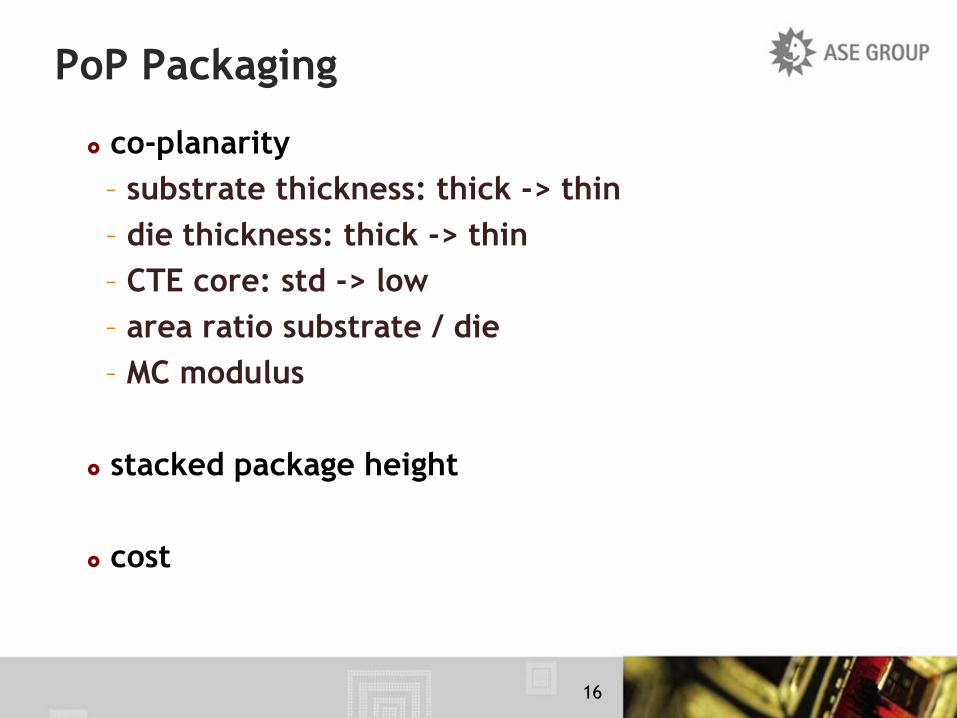
PoP Packaging
co-planarity
– substrate thickness: thick -> thin
– die thickness: thick -> thin
– CTE core: std -> low
– area ratio substrate / die
– MC modulus
stacked package height
cost
16

17
Substrate Development Trends
Low-CTE substrate core
CTE: 12 ppm/C < 10 ppm/C
High interconnect density
Bump pitch: 150 m 130 m
(alternative solutions for pre-solder?)
Stacked via: 3 stacked 4 stacked
Thin substrate
Core thickness: 400 um 200 um 100 um Coreless
800-m core 400-m core Coreless
…
Pre-solder
CoreBlind via

18
BGA Warpage Reduction Guideline
Warpage due to CTE mismatch
Cooling to room temp. Convex shape
Determine the position of
neutral surface
C.L: Centerline
N.S: Neutral surface
Substrate
Silicon
C.L
N.S
C.L
N.S
Moment
Shrinkage
Thick substrate small warpage Thin substrate big warpage
Substrate with Low CTE, High Modulus and Great Thickness are
preferred to reduce package warpage
Shrinkage from each
component
Force/Moment balance to
determine warpage
Dependent on package modulus
and thicknessDependent on package CTE

3D- packaging
micro-bump assembly for TSV
19
•TSV Middle-End High AR Microbump 1st article prototype of 20um size/ 56um height
Joined fine pitch micro bumps
40u
m

Wire Bond Challenges for lowK
Cu wire
– higher force
– CUP
– fine pitch: 1 mil -> 0.8 mil -> 0.7 mil
After ball shear test
Al
– High energy transformation
capillary.
– Parameter optimization.
– Ball shape control.
– Ball shear inspection.
CUP Design & LowK Wafer

PBGA & CSP Packaging
Structure:
– 2L thin: 130µ -> 110µ -> 100µ -> 90µ
– L/S pitch: 50/50 -> 40/40 -> 30/30 -> 20/20
Cost, cost, cost, …
– strip size: std -> MAP -> LMAP – XLMAP
– 2L -> 1L
– 4L -> 2L
– NiAu -> ENEPIG
21

22
Maximum warpage for different BT/Soldermask thickness
Detailed modeling of substrate
Thicker BT - Reduces substrate warpage
Thinner BT - Soldermask thickness has significant impact on substrate warpage
Warpage contours
Warpage of Bare Laminate Substrate
Chip side (soldermask thickness=30um)
-400
-300
-200
-100
0
100
200
300
400
0 100 200 300 400
BT thickness (um)
Max
imum
war
pag
e (u
m)
Ball side (soldermask thickness=15um)
Ball side (soldermask thickness=30um)
Ball side (soldermask thickness=45um)

23
Package Outline
Total
Thickness
Mold Cap
Thickness(A)
Substrate
Thickness(B)
Stand
Off(C)
0.6 mm Max. 0.3 mm 0.095mm 0.17mm Max.
Ball
Size
0.25mm / 0.25 mm
0.8 mm Max. 0.45 mm 0.095mm 0.23mm Max.0.3mm / 0.275 mm
1 mm Max. 0.54 mm 0.095mm 0.29mm Max.0.35mm / 0.3mm
BPO
a-S3 Package outline & X-section
A
B
C
0.5 mm Max. 0.25 mm 0.085mm 0.14mm Max.0.25mm / 0.3 mm

24
Save the package size
Save the wire
Enhance the BLR performance
Allow more lead count
Package
type
Package
size
Ball/ Lead
count
Ball
pitch
Max.
wire length
3D total
wire length
QFN 9x9mm 64 0.5mm 3500um 213 mm
LGA (S3) 9x9mm 64 0.5mm 323um 47 mm
BGA (S3) 8x8mm 105 0.5mm 323um 47 mm
BGA (S3) 6x6mm 64 0.65mm 1183um 88 mm
Feasibility study cases—3 (for Middle lead count QFN)
a-S3 option-1
a-S3 option-2
a-S3 option-3

25
Summary
Meeting the challenges from ELK and Pb-free bumps,
chip-package-system co-design is essential
As the interconnect pitch decreasing, warpage control
is getting critical
Advanced modeling is the one of the keys for warpage
control
Materials properties need to be planned & developed
methodically

26
Thank You
www.aseglobal.com