scanned probe microscopy (spm)€¢ many interesting physics at shorter lengthscales • much...
TRANSCRIPT

Scanned Probe Microscopy
(SxM)
Kyle McElroy

Outline
• Optical microscopes
• Basic principles STM – Piezoelectrics
– Tunneling
– Feedback
– Some results
• S(insert measurement)M – SQM/SHM
– AFM
– NSOM
– SHM

• How do optical microscopes measure?
• What do they measure?
• Limitations of this?
Optical Microscopes and nano-
scale
Lengthscale, l ~ 300-800nm
Measure changes in e

• Many interesting physics at shorter lengthscales
• Much interesting physics doesn’t directly effect e
• How do you get smaller and what else can you measure? – Need control of nm distances
– Turn distance into a Voltage we like Voltages!
Optical Microscopes and nano-
scale

Piezoelectricity
• Electric dipole
linked to lattice
– Applications in sensors, lighters, actuators
– Length-scales involved can be ~nm/V
• Ordered domains
(like ferro-
magnetism)
• Electric field ≈
strain ≈
displacement

Scanning Tunneling
Microscopy

Tunneling
• QM and wave-functions
• Transmission through
barrier ~
• WKB approximation gives:
z
YI YB YT f
)(20
Emz
f
0/ zze
Exponential in barrier thickness
Lengthscale ~1Å

Scanning Tunneling Microscopy
•Sharp tip vacuum
sample tunneling
•Piezo actuator (high
Voltage)
•Measure tunneling
current (S/N)
•Computer acquisition

Feedback
•1Å is small
-1% of that is 10 fm
•Vibration kills
•Feedback protects
-Large gain can be
thrown out to gain
stability and linearity
1V~1nm ~10Å ~20,000 increase in current

STM results
• Atomic lattices and surface structure
Si(111) 7x7 reconstruction
Trenary: UIC
Gold surface
B. Barker: LPS
0
300 Å

STM results
• Atomic lattices and surface structure
Charge Density Wave
on TaSe2
Jixia Dai Colorado
0
300 Å
0
2
00 Å
Can selectively “write” on surface
~10nm lengths

STM results
• Electrons are waves
Fe on Cu(111)
D. Eigler: IBM Almaden
? on Cu(111)

Spin polarized Tunneling
• Aligned spin states means
more DOS for up than
down spins in both.
– Tunneling is easier!
• Misaligned spin states?
Less DOS for tunneling
electron
– Less tunneling.
z
z

Nano magnetics
• Spin polarized
Wiesendanger: Hamburg
Tunneling does not change spin. If tip like a
particular spin you van image the spin order
in a surface

Other scanned probes
S(X)M

Atomic Force Microscopy
Small tip
Force on tip bends
cantilever and deflects
laser
Floppy cantilever
k small

Atomic Force Microscopy
lambda-phage DNA in buffer
human lymphocyte chromosomes
Atomic resolution mica
JPK Instruments
Force curves
Sacrificial bonds in bone
Hansma, UCSB

MFM
• Manipulation of vortices
K Moler: Stanford
CoPt Wiesendanger: Hamburg
• Magnetic Domain
growth

SQM and SHM
• Magnetic field and vortices
K Moler: Stanford

NSOM
• Back to e, both read and write
Before and After Images of Spatial Hole-Burning of
PIC/PVS Molecular Yarn
Topography of a Small PIC Dye Crystal; (K) NSOM Fluorescene
Image of Crystal in Fig. 1J; (L) NSOM Image of 620 nm Emission
from Crystal in Fig. 1J.
Paul F. Barbara, UMM

Nanoscale manipulation
• If you can measure it you can interact with
it
Conclusion
• If you can get a small signal out of it
• If you can make it small and put it on the
end of a piezo
You can use it to measure things on nm
lengthscales.

What else can you measure
with an STM?
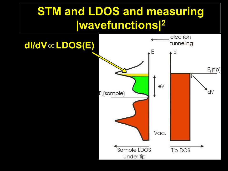
STM and LDOS and measuring
|wavefunctions|2
•Apply Vb
lower EF of sample
by eVb
•Measure I(Vb)
0z
zeV
0
eLDOS(E)dEI(V)
LDOS(E)dI/dV

Our STMs
•5-150 K
•Cryogenic, UHV.
•Low noise or high bandwidth capabilities
•Unique controller architecture allows more data
taking options
•Homemade sound room and vibration isolation
Capabilities at Colorado

91114I02
5.5” sq at
1.5”, 2.75”
0 560 Å
0
5
60
Å
Bi2Sr2CaCu2O8+d
Topography 0 256 Å
0
2
56
Å
0
64 Å
0
6
4 Å
Each bright spot
is a Bi atom --
Cu atom is about
5Å below

Why measure wavefunctions?
• Impurity states
Bi2Sr2Ca(Cu1-xNix)2O8+d : x 0.5%
256 Å, 4.2 K
100 pA, -100 mV
LDOS +9meV
2
)9~,( meVEr +Y

91118a00 -9mV 91118a00 +9mV
91117h14 a
b
• Impurity states
+9 mV -9 mV
3nm field of view,
structure of impurity
state seen
2
)9~,( meVEr Y
Why measure wavefunctions?
Typical FOV
0.4 nS
0.7 nS
400 Å
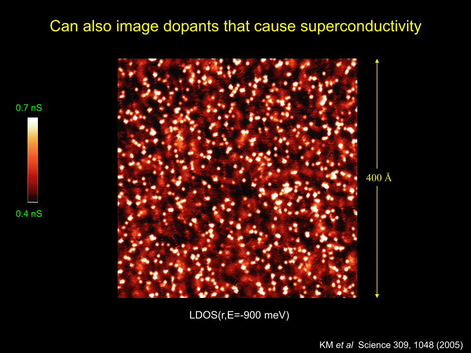
KM et al Science 309, 1048 (2005)
Can also image dopants that cause superconductivity
LDOS(r,E=-900 meV)