scanning probe microscopies (spm) - unigerocca/didattica/laboratorio/s in... · scanning probe...
TRANSCRIPT

Scanning Probe Microscopies (SPM)
Nanoscale resolution af objects at solid surfaces can be reached with
scanning probe microscopes. They allow to record an image of the surface
atomic arrangement in direct space avoiding complicated calculations to
invert the experimental result from reciprocal space measurements.
All SPM have in common the necessity to place a tip placed at atomic
distances from a surface using piezoelectric elements.
The observed quantities may be:
-Tunneling current (Scanning tunnelling Microscope, STM)
- Photon emission (single molecule Raman spectroscopy)
- Deflection of a cantilever (Atomic Force Microscope, AFM)
- Local work function (Kelvin Probe)
- Optical response (Scanning Near Field optical microscope, SNOM)

STM: working principle
What is imaged is the convolution of the density of electronic states of surface and tip, making use of the tunneling current between the metallic tip and a conductive substrate.
If a metallic tip, terminated ideally with one single atom, is brought to a distance of few Å from a surface and polarized by a bias voltage, electrons may tunnel through the vacuum. Since the process is strongly localized what matters is the density of states at tip and surface and lateral resolutions of just a few Å can be achieved (atomic resolution). Mapping the tunneling current vs x-y coordinates gives an image of the electronic state density at the surface (either empty or filled depending on the direction of the current).

STM: images
a0
b0
Atomic resolution at Ag(110)
Atomic resolution of adsorbates at Ag(110)
Ice cluster on Cu(111)
Glutamic acid at Ag(100)

The tunneling effect had been known for decades but STM was invented only in 1981 by Binning e Roher (Physics Nobel Prize winners in 1986). Why did mankind need so long to move this step forward?
Solution was needed for non trivial problems

STM: stability
Mechanical stability
- Compact design;
-The microscope is fixed to the apparatus with springs with risonance frequency of just few Hertz;
- Permanent Magnets attenuate vibrations generating “eddy currents”;
- Pneumatic feet decouple the apparatus from the pavement.
Createc STM apparatus at
the University of Genoa

STM: feedback circuit

STM: scanner designs

STM: scanning methods
Dz
Constant current (nA). The feedback is active and the tip is elongated or retracted during the scanning.
Constant height (~5 Å).
Feedback inactive.
Quicker, but works only
on atomically flat
surfaces

STM: Theory
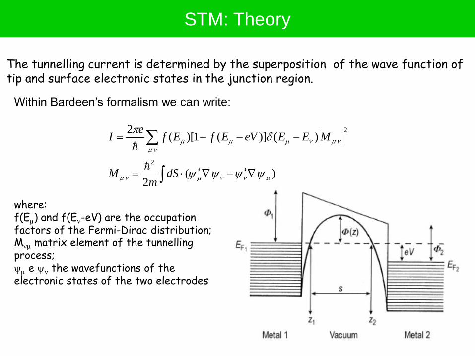
The tunnelling current is determined by the superposition of the wave function of tip and surface electronic states in the junction region.
d
FS
FT Filled Electronic Valence Band States
Potential Barrier Quantum tunnelling off
(no superposition)
Potential Barrier Quantum tunnelling on
(superposition)
e-
d
FS
FT Filled Electronic Valence Band States
STM: Theory
)(2
)()](1)[(2
2
2
dSm
M
MEEeVEfEfe
I
where: f(E) and f(E-eV) are the occupation factors of the Fermi-Dirac distribution; M matrix element of the tunnelling process; e the wavefunctions of the electronic states of the two electrodes
The tunnelling current is determined by the superposition of the wave function of tip and surface electronic states in the junction region.
Within Bardeen’s formalism we can write:

STM: Theory
One dimensional barrier (we neglect the electric field in the junction and assume that both electrons have the same work function f). For a barrier width s we get:
)(0
0
zsk
kz
e
e
1.1
22
fmkwith Å-1 for f=4.5 eV
ks
ks
eI
ekdSm
M
22
02
0
002
)(22
So that
Sum over all energy states of energy and occupation number such to be involved in the tunneling process
-| 0|2 and |
0|2 are the local density of states at tip and surface, respectively
-Removing the dependence on z the current I can be estimated.
-I depends exponentially on barrier width. For k=1.1 Å-1, I varies by one order of magnitude per Å. High sensitivity to the surface corrugation!

e-
d d
Positive Bias Positive Bias
Negative Bias Negative Bias
FS
e- FS
FT
FT 1eV
Tip Sample Sample Tip
Filled Electronic Valence Band States
STM: scheme of the energy bands

STM: spatial resolution
Tersoff-Hamann model: The tip is described by a sphere of radius R (R0) placed in r0.
)()(2
0 FEErI
I is proportional to the local density of states of the sample in r0. The formula can be rewritten for a spatially extended tip, considering R+d the tip-surface distance. (large R smaller sensitivity to surface corrugation).
Where: hs = corrugation amplitude; a = periodicity along the surface; Δd = apparent observed corrugation; R = radius of the tip; d = tip surface distance a = lattice spacing
hs ampiezza della corrugazione a periodo della corrugazione superficiale Δdampiezza di corrugazione osservata R raggio della punta
Analitic form for the corrugation amplitude:

STM: Examples - surface reconstructions
Si(111)-(7x7) Surface
Sticks-and-Balls Model STM Image
O-Ag(110) added row reconstruction

How complicated can be a simple system?
O adsorption on Ag(110) for low temperature dissociation

<0-1
1>
a b
<0-1
1>
a b
. 5. Coexistence of flower-like and square-like structures upon Glu
deposition on Ag(100) at T=350 K. The two arrangements are present
either as well separated island with defined structure (panel a) or as
small aggregates in which they are intermixed (panel b). a) Image size
188 Å x 188 Å, V=0.17 V, I=0.3 nA; b) image size 94 Å x 94 Å, V=-1.0
V, I=0.3 nA (L. Savio et al. 2012)

STM: manipulation
Manipulation of weakly bound atoms/molecules adsorbed at
a solid surface allows to organise them in particular
arrangments. The STM tip is used to lift and put down the
atomic units or to move them by pushing or pulling.

Fe/Cu(111)
Confinement of electrons in quantum corrals at a
metal surface.
Standing waves - Interference patterns
Cu(111) surface state electrons form a 2Dim, quasi-free electron gas. Their
scattering off point defects, steps, adsorbates etc. generates standing wave
patterns in the electron density, which can be investigated by STM.
STM: manipulation

V,I
Vertical manipulation
F. Moresco et al., PRL 86, 672 (2001)
Porfirin on Cu(111) behaves like a molecular switch if tension pulses are applied to it via the STM tip
STM: manipulation

N
N
19Å
17Å
esa-tert-butil-pirimido-pentafenilbenzene
(HB-NPB)
benzene
Lateral phenyl ring
tert-butilic group (leg)
Marker: pyrimidine

20 Å
single HB-NPB
molecules on Cu
F. Moresco et al Nature
nanotech 2006
Cu HB-NPB
Dim.: 32 nm x 32 nm; STM parameters: I = 110 pA; V = 2,2 V
STM: manipulation

STM: manipulation

STM: manipulation
Lander molecule on Cu(111).
Column A: at (111) terrace;
columns B and C: contact to (100) step.
The molecular board is either parallel (B) or
orthogonal (C) to the step. Only in the latter
case an influence becomes visible on the
upper terrace. In (C2) and (C3), an
additional bump corresponding to the
contact point of the wire to the step appears
and in (C4) a modification of the upper
terrace standing wave patterns is visible.
Row1: Sphere models of optimized
molecular structures. Row 2: Calculated
STM images, corresponding to the models
above. Row 3: STM measurements. Black
to white distance 3.5 A, V=0.8 V, I=0.2 nA,
T=8 K.
Line 4: Pseudo-three-dimensional STM
measurements visualizing the standing
wave patterns. V=0.1 V, I=0.2 nA, T=8 K.
F. Moresco et al., PRL 91, 036601 (2003).
Electrical contacts
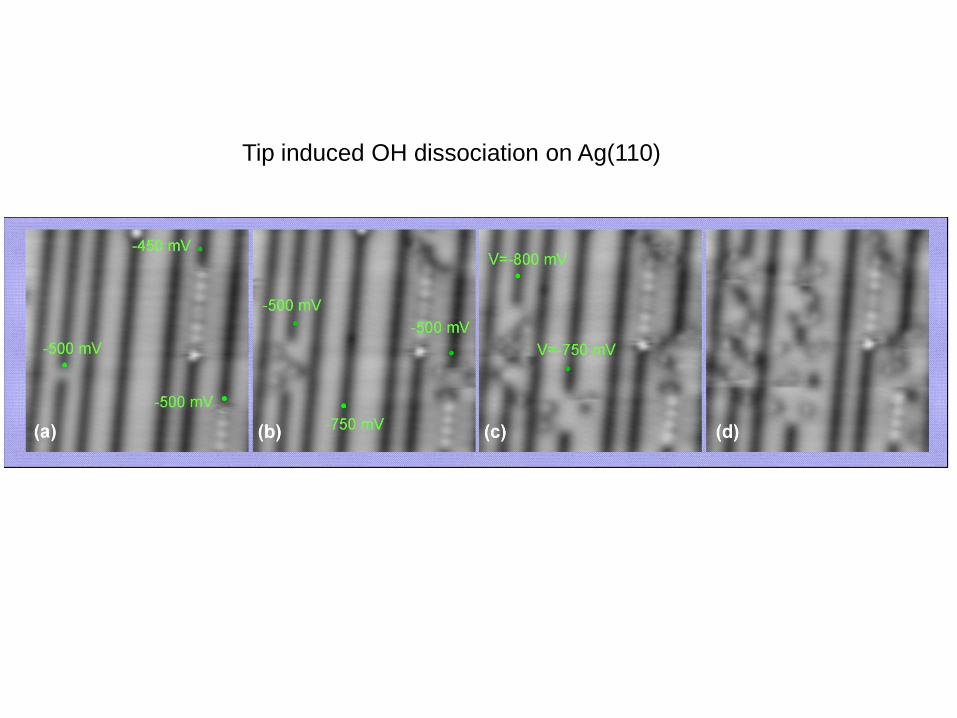
Tip induced OH dissociation on Ag(110)

Scanning Tunnelling Spectroscopy
deUTneUnI s
eU
t ),()()(0
Where: nt, ns = density of states of tip and sample; U = bias voltage; T = transmission coefficient (tunnelling matrix)
),()()0()( eUeUTeUnenUdU
dIst
Differentiating with respect to U
(considering T(,eU) constant)
The measured property (conducibility) is in good approximation proportional to the density of states of the sample. In the limit of small bias voltage (a few V), when the junction has an ohmic behavior, one plots usually (dI/dU)/(I/U). In this way one eliminates the exponential dependence of the current on the barrier thickness.

Si(111)-(2x1)
Unoccupied States
Occupied States
Scanning Tunnelling Spectroscopy
Experiment
Theory

Carbon Nanotubes
Scanning Tunnelling Spectroscopy
Measurement of the gap of the nanotubes The magnitude of the gap depends on the diameter of the nanotubes

Inelastic ElectronTunnelling Spectroscopy
For bias values eV>h, the excitation of a vibrational mode of frequency of an adsorbed molecule or of the substrate becomes possible . The opening of the inelastic channel implies an increase of the total tunnelling current, causing a jump in the conducitivity and a peak in the second derivative (d2I/dV2).
Single molecule vibrational spectroscopy. The chemical sensitivity allows for an additional contrast in the STM images.

Inelastic ElectronTunnelling Spectroscopy
W. HO, PLR 87, 166102 (2001)
STM topographical images (bare tip, V=70 mV, I=1 nA)
showing the manipulation of a CO molecule toward two O
atoms co-adsorbed on Ag(110) at 13 K. (A) A single CO
molecule and two O atoms. (B) The CO is moved toward O
atoms by applying sample bias pulses (1240 mV) after
positioning the tip over it. (C) The CO was moved to the
closest distance from the two O atoms to form the O-CO-O
complex. (D) A CO2 molecule is desorbed by an additional
voltage pulse and the remaining O atom is imaged. (E) STM-
IETS Spectra over the CO along the reaction pathways (I, II,
and III). The peak (dip) at positive (negative) bias is assigned
to the hindered rotation mode. The vibrational assignment is
supported by isotopic shift. The voltage position of the peak
is 2 mV higher than that of the dip, due to changes in the
interaction between the CO and the surface under different
bias polarities. No significant differences in the line shape
and position of the peak or dip are observed between
spectra I and II as well as for isolated CO molecules. The
mode shows an up-shift of 4 meV, a decrease in intensity,
and a line shape broadening for the O-CO-O complex (III).
The spectra displayed are averages of multiple scans from -70 mV to
+70 mV and back down and subtracting the background spectra taken
over clean Ag(110). Dwell time of 300 ms per 2.5 mV step and 7 mV
rms bias modulation at 200 Hz were used for recording the spectra.
29 Å x 29 Å

Inelastic ElectronTunnelling Spectroscopy
a) I –V curves recorded with the STM tip directly
above the center of a C2HD molecule (1) and
above the bare copper surface (2). The difference
curve (1–2) is also shown. Each scan took 10 s.
b) dI/dV curves recorded directly above the center
of the molecule (1) and above the bare surface (2).
The difference spectrum (1–2) shows two sharp
increases (arrows).
c) d2I / dV2 recorded simultaneously with the data in
b) directly above the molecule (1) and above the
bare surface (2). The difference spectrum shows
peaks at 269 and 360 mV, resulting from the C–D
and C–H stretch excitations, respectively.
Acetylene on Cu(100)

Inelastic ElectronTunnelling Spectroscopy
Octanedithiolate (-SC8H16S-) bonded to gold electrodes.

Atomic Force Microscopy
The parameter is the force between tip and surface

No interaction no deflection of cantilever
attractive region negative deflection of cantilever
Repulsive region positive deflection of the cantilever
where: s = distance tip sample; σ = distance at which U(σ) = 0; –ε = energy at the equilibrium position
U(s) = 4ε[(σ/s)12 – (σ/s)6]
AFM: tip-surface interactions
Interaction energy
The derivative dU/ds is in first approximation the force between
tip and sample
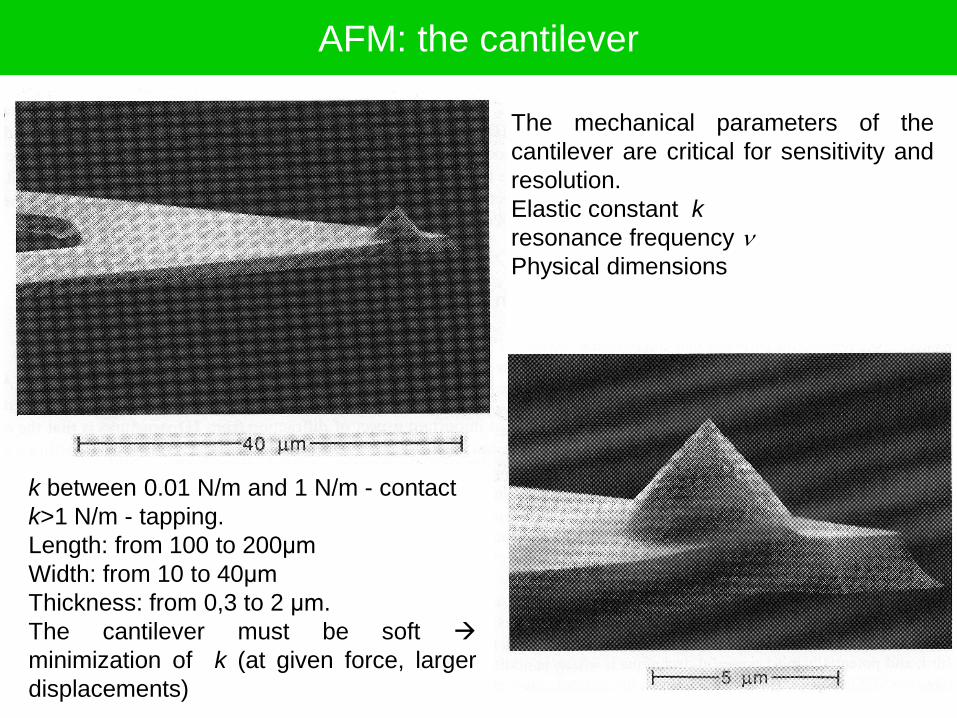
AFM: the cantilever
The mechanical parameters of the
cantilever are critical for sensitivity and
resolution.
Elastic constant k
resonance frequency
Physical dimensions
k between 0.01 N/m and 1 N/m - contact
k>1 N/m - tapping.
Length: from 100 to 200μm
Width: from 10 to 40μm
Thickness: from 0,3 to 2 μm.
The cantilever must be soft
minimization of k (at given force, larger
displacements)

AFM: the cantilever
The tip must be sharp to evidence the irregularities of the surface and must be tight for not breaking when it comes in contact with the surface.
-The radius of curvature determines the lateral resolution on a flat surface. More recent techniques allowed to prepare tips with r ≈ 5nm. - The half-angle θ corresponds to the largest inclination of a wall reproduced by the tip. Typically 10°<θ<45°. - The height h determines the capability to probe deep valleys. The highest vertical extension is usually smaller than 10 μm.
=10°
=45°

STM vs AFM: tip surface interaction
STM
AFM
In AFM images more than one atom contributes to the image. Since they are in different positions, the global signal consists of the sum of such dephased contributions. Atomic resolution may result all the same

AFM: measurement methods
Contact mode measurement
-The tip touches the sample, i.e. the tip sample distance is smaller than one atomic radius. - The electrostatic forces acting on the tip are repulsive and have an average value of 10-9 N. - This mode is used to investigate the friction force at the nanoscale by evaluating the lateral deflections of the tip.
Constant force • Slower (feedback on) • Small friction forces
Constant height • quicker • large friction forces

Tapping mode
The tip is maintained in a forced oscillation at a frequency close to
resonance and kept constant by a feedback system. The deviation
from the resonance frequency due to the Van der Waal forces
between tip and sample allow to perform an image the surface
Amplitude of the oscillation of the tip: 1-10 nm. Sample – tip distance : 1-40 nm Resonance frequency: 50-500 kHz; depending on the sample characteristics. Narrow resonance peak under vacuum conditions, larger for AFM measurement in air.
No-contact mode
- Tip- surface distance: 5-15 nm. - Van der Waals forces, electrostatic and capillar forces.
AFM: measurement methods

Amplitude modulation (AM)
The cantilever is put at a fixed vibrational frequency close to resonance and the variation of the vibrational amplitude is recorded. The amplitude of the modulation of the cantilever depends on the elastic properties of the sample.
AFM: measurement methods
Amplitude of
the vibration Frequency
shift at
resonace shift in
amplitude
frequency
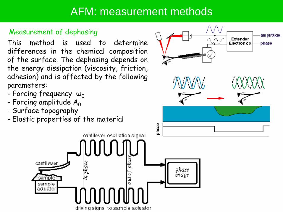
Measurement of dephasing This method is used to determine differences in the chemical composition of the surface. The dephasing depends on the energy dissipation (viscosity, friction, adhesion) and is affected by the following parameters: - Forcing frequency ω0
- Forcing amplitude A0
- Surface topography - Elastic properties of the material
AFM: measurement methods

AFM: examples
Steps on a Si (111) surface (10 m x 10 m)
Graphite surface The AFM image shows all atoms within the hexagonal unit cells.
2×2 nm2
From http://www.physik.uni-regensburg.de/forschung/giessibl.shtml
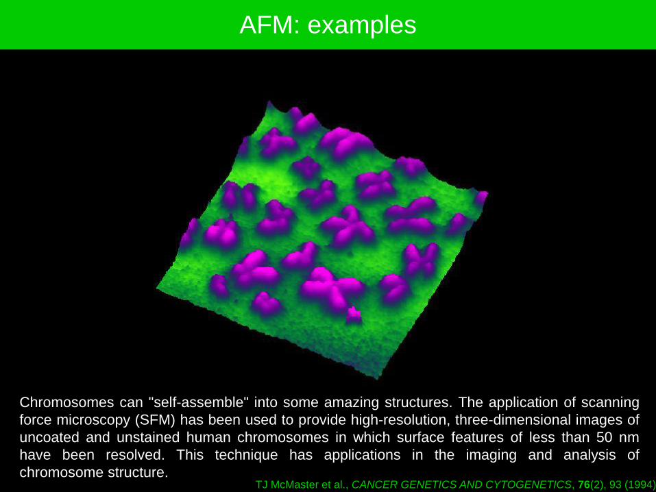
AFM: examples
Chromosomes can "self-assemble" into some amazing structures. The application of scanning
force microscopy (SFM) has been used to provide high-resolution, three-dimensional images of
uncoated and unstained human chromosomes in which surface features of less than 50 nm
have been resolved. This technique has applications in the imaging and analysis of
chromosome structure. TJ McMaster et al., CANCER GENETICS AND CYTOGENETICS, 76(2), 93 (1994).

• Measurement of current;
• Conducting and semiconducting surfaces;
• Atomic resolution;
• Allows manipulation;
• Allows electronic and vibrational spectroscopy of individual molecules (chemical sensitivity);
• Vacuum is not necessary;
• The interaction may damage the sample.
STM vs AFM
STM
• Measurement of force;
• Any surface;
• Good resolution, sometimes at atomic level;
• Allows manipulation;
• Topographic information and measurement of friction forces;
• Chemical sensitivity in the tapping mode (Kelvin microscopy)
• No necessity for vacuum except to keep surface in controlled state;
• Non destructive, allows to investigate biological samples
AFM

Near Field Scanning Optical Microscopy NSOM
Light microscopes are limited in
resolution to half the wavelength
of light (Abbe) i.e. 200 nm for
visible light.
This isn’t true, however, in the
near field. Ash and Nichols
demonstrated in 1972 that /60
can be reached with 3 cm
microwaves.
