screen printed thermoelectric devices712773/fulltext01.pdf · thermoelectric materials are not...
TRANSCRIPT

Linköping Studies in Science and Technology
Licentiate Thesis No. 1663
Screen Printed Thermoelectric Devices
Andreas Willfahrt
Dept. of Science and Technology
Linköping University, LiU Norrköping
SE-‐601 74 Norrköping
Norrköping 2014

II
© Andreas Willfahrt, 2014
Printed in Germany by Stuttgart Media University
ISSN 0280-‐7971
ISBN 978-‐91-‐7519-‐323-‐6
III
Screen Printed Thermoelectric Devices
By
Andreas Willfahrt
April 2014
ISBN 978-‐91-‐7519-‐323-‐6
Linköping studies in science and technology
No. 1663
ISSN 0280-‐7971

V
ABSTRACT
Thermoelectric generators (TEG) directly convert heat energy into electrical energy. The impediments as to why this technology has not yet found extensive application are the low conversion efficiency and high costs per watt. On the one hand, the manufacturing process is a cost factor. On the other, the high-‐priced thermoelectric (TE) materials have an enormous impact on the costs per watt. In this thesis both factors will be examined: the production process and the selection of TE materials. Technical screen printing is a possible way of production, because this method is very versatile with respect to the usable materials, substrates as well as printing inks. The organic conductor PEDOT:PSS offers reasonable thermoelectric properties and can be processed very well in screen printing. It was demonstrated by prototypes of fully printed TEGs that so-‐called vertical printed TEGs are feasible using standard graphic arts industry processes. In addition, the problems that occur with print production of TEGs are identified. Finally, approaches to solve these problems are discussed.
Keywords: screen printing, thermoelectric generator, Seebeck effect, energy harvesting

VI
Acknowledgement
I feel great gratitude to those who have enabled me to work on this thesis. Since I am an external PhD student my thanks go to both working groups in Norrköping and in Stuttgart, Germany.
First and foremost I want to thank my supervisor Xavier Crispin, who shares the vision of printed thermoelectric generators with me, providing the basis for this work. The very first person for discussions in Germany is Erich Steiner, an enthusiastic scientist unfortunately retiring soon.
During my stays in Norrköping I can count on my fellow students, who have enriched my work and leisure time with their support. Thank you Olga, Zia, Hui, Skomantas and all the others. And of course I am very grateful to my working group in Germany, headed by Gunter Hübner, for discussions and practical help during the busy project phases.
And not to forget Sophie Lindesvik, who is always helping with administrative issues as well as Kirsten Magee, who had to struggle with proofreading the final draft.
Finally, I want to express my deepest gratitude towards my wife Karen and my daughter Marie, who enrich my life in a unique way.
Stuttgart, April 2014
Andreas Willfahrt

VII
Table of Contents I Background .................................................................................. 1 Introduction ....................................................................................................... 2 1 Fundamentals .................................................................................................... 5
1.1 Thermoelectricity .................................................................................................. 5 1.1.1 Seebeck Effect ................................................................................................................ 5 1.1.2 Peltier Effect ................................................................................................................... 6 1.1.3 Kelvin Relations ............................................................................................................ 6 1.1.4 Basic Thermoelectric Equations ............................................................................ 7 1.1.5 Thermoelectric Generator and Cooler ................................................................. 7 1.1.6 Thermoelectric Materials .......................................................................................... 9 1.1.7 Design of TEGs ............................................................................................................ 13
1.2 Screen Printing .................................................................................................... 14 1.2.1 Screen Preparation ................................................................................................... 16 1.2.2 Imaging and Screen Development ..................................................................... 17 1.2.3 Printing .......................................................................................................................... 17
1.3 Rheology ................................................................................................................. 18 1.3.1 Viscosity ......................................................................................................................... 19 1.3.2 Thixotropy .................................................................................................................... 20 1.3.3 Levelling ........................................................................................................................ 20 1.3.4 Viscosity of Particle Filled Printing Inks .......................................................... 21
2 Printing Inks and Substrates ..................................................................... 23 2.1 Metal-‐Filled Functional Printing Inks .......................................................... 23
2.1.1 Thermoplastic and Thermosetting Binders ................................................... 24 2.1.2 Conduction Mechanism ........................................................................................... 25
2.2 Printable Thermoelectric Materials ............................................................. 26 2.2.1 Bi and Sb Containing Printing Inks .................................................................... 27 2.2.2 Nickel Printing Inks .................................................................................................. 27 2.2.3 Conducting Polymers ............................................................................................... 28
2.2.3.1 Conjugated Polymers ...................................................................................... 29 2.2.3.2 Conduction Mechanism in Conjugated Polymers ............................... 30 2.2.3.3 Doping of Conjugated Polymers ................................................................. 31
2.3 Insulators and Substrates ................................................................................ 34 2.3.1 Printable Dielectrics ................................................................................................. 34
2.3.1.1 UV-‐Curable Dielectrics ................................................................................... 34 2.3.1.2 Plastisol Dielectrics .......................................................................................... 36
2.3.2 Flexible Substrates .................................................................................................... 37 3 Experimental Setup ....................................................................................... 38 4 Conclusion of the Published Papers ........................................................ 39 5 Goal of the Thesis ........................................................................................... 40 6 References ........................................................................................................ 41 7 Table of Figures .............................................................................................. 44
II Published Papers ...................................................................... 47

VIII
Abbreviations Al Aluminium Bi Bismuth Cl Chloride CMYK Cyan Magenta Yellow Black – Gamut for Printing CP Conjugated Polymers CTE Coefficient of Thermal Expansion CTF Ceramic Thick Film Cu Copper ICP Intrinsic Conductive Polymer NCP Non Conducting Polymers Ni Nickel PA Polyamide PANI, PAn Polyaniline PCB Printed Circuit Board Pd Palladium PEDOT (Poly)3,4-‐ethylendioxythiophen PET Polyethylene Terephthalate PTF Polymer Thick Film PVC Polyvinyl Chloride Sb Antimony T Absolute Temperature TC Thermocouple Te Tellurium TE Thermoelectric TEC Thermoelectric Cooler TEG Thermoelectric Generator Tg Glass Transition Temperature TTF-‐TCNQ Tetrathiafulvalene-‐7,7,8,8-‐tetracyanoquinodimethane VOC Volatile Organic Compounds Z Figure of Merit ZT Dimensionless Figure of Merit

I. Background
2
Introduction Thermoelectricity describes the direct conversion of heat into electrical
energy (thermoelectric generators, TEG) or vice versa (Peltier device, thermoelectric cooler, TEC). Three thermoelectric effects are known: the Seebeck effect, the Peltier effect and the Thomson effect. The scientist who discovered the phenomena – Thomas Johann Seebeck, Jean-‐Charles Peltier and William Thomson (Lord Kelvin) – gave the effects their names.1 In the scope of this thesis, we focus on the Seebeck effect since it is related to the conversion of thermal energy into electrical power.
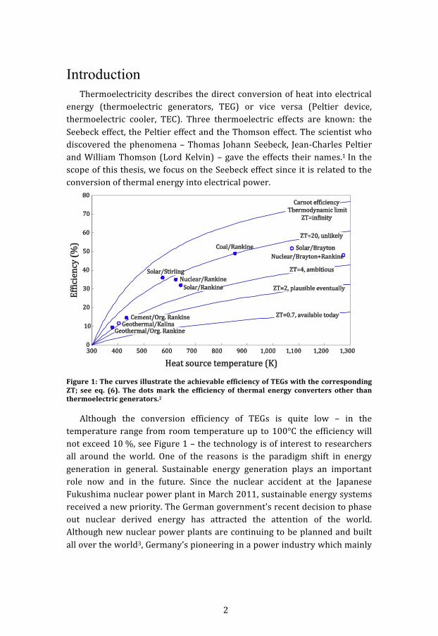
Figure 1: The curves illustrate the achievable efficiency of TEGs with the corresponding ZT; see eq. (6). The dots mark the efficiency of thermal energy converters other than thermoelectric generators.2
Although the conversion efficiency of TEGs is quite low – in the temperature range from room temperature up to 100°C the efficiency will not exceed 10 %, see Figure 1 – the technology is of interest to researchers all around the world. One of the reasons is the paradigm shift in energy generation in general. Sustainable energy generation plays an important role now and in the future. Since the nuclear accident at the Japanese Fukushima nuclear power plant in March 2011, sustainable energy systems received a new priority. The German government's recent decision to phase out nuclear derived energy has attracted the attention of the world. Although new nuclear power plants are continuing to be planned and built all over the world3, Germany’s pioneering in a power industry which mainly

3
relies on sustainable energy sources could become a role model for many countries.
The effective exploitation of energy sources is one of the key factors to a sustainable energy supply. Almost all conversion processes generate waste heat and the extent is also remarkable. For instance, the energy converted by a car is only used to 21.5 % for moving the vehicle. Around 78.5 % is lost as unused heat.4 If waste energy harvesters are used in a large scale for waste heat conversion, an increased total energy balance will be achieved, similar to cogeneration (combined heat and power plant).
Since in many processes thermal waste energy is an unwanted by-‐product, the mass application of TEGs would be very interesting. Thermoelectricity is mentioned in connection with the term “energy harvesting” or “waste energy harvesting”. Energy harvesting (predictable energy source) or energy scavenging (random ambient energy) describes the approach of making energy accessible that normally would be wasted. Different energy harvester designs and principles are known. Thermoelectric generators (temperature gradient required) are amongst piezoelectric generators (mechanical activation required) and well-‐known technologies like wind power (indirect solar) and water power (potential or/and kinetic energy), and photovoltaics (PV, direct solar). While the latter ones produce a considerable high amount of energy, the first two are also called “micro energy harvesters”, since the converted electrical voltages of both piezo-‐ and thermoelectric devices are in the microvolt range. The small amounts of energy are indeed disproportionate to the actual energy demands of specific applications, e.g. powering sensor nodes or the like. Highly sophisticated power management leads to a feasible way to also power such devices by thermoelectric generators.5
However, a high cost per watt is an exclusion criterion so far. An inexpensive way of production would be a huge step towards the mass application of TEGs. One approach to reduced manufacturing costs is the structuring of TEGs by means of printing technology. Printing methods provide a fast and rather inexpensive way of production if compared to other methods, e.g. vacuum deposition. Additionally, costs for thermoelectric (TE) materials must also be reduced. Organic conductors could be a way to cheaper TE materials.6
Fully printed TE devices enable decreasing costs and beyond that, provide the possibility of using flexible substrates in order to establish bendable TEGs. In contrast to rigid devices, fully printed flexible TEGs

4
potentially address new markets where rigid TEGs cannot be used conveniently.
The print production of TEGs requires both the availability of printable thermoelectric materials and suitable substrates. Besides the materials, the parameters of printing technology need to be examined, so that an optimized workflow is set up. In this thesis, we have investigated both materials and process engineering. Commonly used thermoelectric materials are not available as printing inks for screen printing. Individual ink formulations are therefore necessary in order to build a TEG-‐prototype with reasonable thermoelectric properties.
In general, it is challenging to establish functional printing inks. If bulk materials are used as fine particles in the binder-‐solvent mixture or the TE materials are solution processable, e.g. intrinsic conductive polymers, a thermal treatment is needed for evaporation of the solvents used in the ink. Additionally, a densification of the printed ink film is favourable for metal-‐filled inks, as shown in 2.1.2. It is possible to achieve a densification by thermal treatment.
After finding the appropriate inks the parameters of screen printing are optimized for these inks. The adjustment of the printing process parameters mainly concerns the screen making and the printing process itself, the successive process steps are less important in the first instance. However, the post-‐press treatment becomes important when a prototype could be built up and the move from the prototype to production is planned. In that way, the processability of the deployed materials is also an issue during the prototype creation.

5
1 Fundamentals
1.1 Thermoelectricity
Three thermoelectric effects named after their discoverers Thomas J. Seebeck, Charles A. Peltier and William Thomson (Lord Kelvin) are linked by the Kelvin relations. The Seebeck effect has gained much interest in the past, since it is the underlying principle of converting thermal energy directly into electricity. Thermoelectric generators (TEGs) based on the Seebeck effect have no moving parts and are maintenance free devices, important issues for long-‐term usage in harsh environments. TEGs were therefore used in NASA space missions7, for instance. Nowadays, TEGs are recovering some energy in the combustion system of cars.8
The reverse effect was found by Peltier. Thermoelectric coolers (TECs, Peltier element) are used in portable refrigerators or in lab devices for cooling purposes. Thomson developed the Kelvin relations and predicted the Thomson effect that describes the reversible heat transport in a conductor in which an electrical current flows. The Thomson effect will not be investigated further in the scope of this thesis, since its practical use is rather limited. The Kelvin relations are the link between all three thermoelectric effects.
1.1.1 Seebeck Effect
If the ends of a metal rod or wire are held at two different temperatures, the electrons on the hot side have more kinetic energy than on the cold side. Thermodiffusion between the hot and the cold side develops until the electric field prevents further separation. Hence, the electric potential at the cold side is more negative than of the hot side.
Figure 2: Kinetic energy of electrons depicted by arrows of different lengths (left). The electrons accumulate at the cold side.9
A thermoelectric voltage is developed between the positively charged hot end and the negatively charged cold end, due to the potential difference. The potential difference (open circuit) is a material parameter called Seebeck coefficient:

6
𝑆𝑆 =𝑑𝑑𝑑𝑑𝑑𝑑𝑑𝑑
(1)
with Seebeck coefficient S, potential difference dV and temperature gradient dT.
1.1.2 Peltier Effect
The basic principle of a Peltier element is a current flow that generates a temperature difference. The electric current passing a junction of two dissimilar conductors (metals, semimetals or semiconductors) releases or absorbs heat at the junction. There are two effects which can be summed up as the irreversible Joule heating and the reversible Peltier heating. “From this follows that the degree of cooling which can be obtained by using the Peltier effect is limited to the point at which the Joule heating begins to predominate.”10
1.1.3 Kelvin Relations
Lord Kelvin showed that there is interdependency between the thermoelectric effects. The general equations are
𝚤𝚤 = 𝜎𝜎(𝐸𝐸 − S∇𝑇𝑇) (2)
𝑞𝑞 = 𝑆𝑆𝑆𝑆𝚤𝚤 − 𝜆𝜆∇𝑇𝑇 (3)
with electric current density 𝚤𝚤 , heat current 𝑞𝑞 , electric conductivity σ, thermal conductivity λ, the electric field 𝐸𝐸 , Seebeck coefficient S and temperature gradient 𝛻𝛻𝑇𝑇. If only one dimension is considered, eq. (2) and (3) are changed to
𝐽𝐽 = 𝜎𝜎𝑑𝑑𝑑𝑑𝑑𝑑𝑑𝑑
− 𝑆𝑆𝑑𝑑𝑑𝑑𝑑𝑑𝑑𝑑
(4)
𝑄𝑄 = −𝜆𝜆
𝑑𝑑𝑑𝑑𝑑𝑑𝑑𝑑
+ 𝑆𝑆𝑆𝑆𝑆𝑆 (5)
with current density J, heat flow density Q and Temperature T in Kelvin. Thus, the heat current must be maintained in order to achieve a thermoelectric current.

7
1.1.4 Basic Thermoelectric Equations
The performance of TE materials is determined by a dimensionless figure of merit ZT defined as
𝑍𝑍𝑍𝑍 =𝑆𝑆!𝜎𝜎𝜆𝜆𝑇𝑇 (6)
The numerator S2σ is called power factor. ZT is an important parameter for comparing TE materials. The Seebeck coefficient to the power two is dominating the equation, but the quotient of electrical and thermal conductivity is also crucial. TE materials with high Seebeck coefficients have high electrical conductivities and low thermal conductivities. This may be a conflicting requirement that is not fulfilled by metals, for instance, see Table 1.
Table 1: Thermal and electrical conductivities of selected materials.11
Material Thermal conductivity λ [Wm-‐1K-‐1]
Electrical conductivity σ [S m-‐1]
Cu 395 59x106
Glass 0.7 -‐ 1.1 1x10-‐11 -‐ 1x10-‐15
Al2O3 (ceramic) 25 -‐ 35 1x10-‐14 -‐ 1x10-‐15
The theoretical maximum efficiency of a heat engine like a TEG is determined by the Carnot efficiency ηcarnot
𝜂𝜂!!"#$% =𝑇𝑇! − 𝑇𝑇!𝑇𝑇!
= 1 −𝑇𝑇!𝑇𝑇!
(7)
with the temperature at the hot end Th and the temperature at the cold end Tc. The efficiency of a TE device is directly related to ZT. For power generation, the efficiency η is given by
𝜂𝜂 =𝑇𝑇! − 𝑇𝑇!𝑇𝑇!
1 + 𝑍𝑍𝑍𝑍 − 1
1 + 𝑍𝑍𝑍𝑍 + !!!!
(8)
It is important to use materials with a high ZT value for practical applications.12, 13
1.1.5 Thermoelectric Generator and Cooler
If two dissimilar thermoelectric materials are electrically connected, the device is called a thermocouple (TC). The thermoelectric materials are also

8
known as legs, which are characterized by the majority charge carriers accumulating upon thermal diffusion. If the majority charge carriers are electrons that accumulate at the cold end, the Seebeck coefficient of the material is negative. In contrast, if holes accumulate at the cold end, the Seebeck coefficient is positive. This is valid for metals but also for semimetals and semiconductors. Semiconductors are distinguished in p-‐ and n-‐type materials, according to the majority charge carriers. This indication is also common with thermoelectric legs.
When a temperature gradient is applied between the junction and the open ends of the TC, a thermoelectric voltage is created. Many of these TCs electrically connected in series and thermally in parallel are called TEG. The top and the bottom of a TEG are made of a thermally conducting, electrically insulating material, e.g. ceramics, in order to have a low thermal resistance to the TEG, but to prevent short circuits. The designs of either a TEG or TEC are the same, the only difference is that one device is connected to and powering a load; the other one is connected to a current supply, which creates a heat current occurring in the TEC, establishing a hot and a cold side.
Figure 3: A thermocouple illustrated by two dissimilar materials connected by a con-‐ductor (left). An electrical series connection of several to many thermocouples is called thermoelectric generator.
In the conventional TEG/TEC production the thermoelectric material bismuth telluride (Bi2Te3) is commonly used for low temperature applications (<200 °C). A combination of an electron conducting n-‐type material and a hole conducting p-‐type material represents the thermoelectric legs of a TC.13 A good electrical conductor, e.g. copper or silver, connects the legs. The dimensions of the legs are in the order of millimetres to ensure a large temperature gradient.14 The series connection is realized by a three-‐dimensional meander structure with alternating electrical connections on the top and bottom of the device.

9
1.1.6 Thermoelectric Materials
It is obvious from eq. (6) that reasonable thermoelectric materials show a high electrical conductivity σ and a low thermal conductivity λ. The material researchers in thermoelectricity aim for “electron crystals” and “phonon glasses”, i.e. the material should have the electrical conductivity of crystalline metals and the low thermal conductivity of glass.
The electrical conductivity σ depends on the electronic properties of the material. Metals yield high electrical conductivity, since the conduction band is partly filled, allowing the electrons to move freely along the crystal structure of the metal. The electrons are referred to as free electron gas, if no interactions between the lattice ions are considered. In this simple model, the thermal conductivity of metals is virtually only depending on the free electrons, so that the thermal conductivity is also high. The total thermal conductivity 𝜆𝜆 = 𝜆𝜆! + 𝜆𝜆! is constituted by the lattice and the electronic thermal conductivity, λL and λE respectively. For pure metals it is valid to assume λE≫λL. The Wiedemann-‐Franz Law defines the dependency of the electrical conductivity σ and thermal conductivity λ in metals
𝜆𝜆𝜎𝜎= 𝐿𝐿𝐿𝐿 (9)
with the Lorenz number L and the absolute temperature T. In contrast, the thermal conductivity of insulators only depends on lattice contribution (phonons).15
The Seebeck coefficient S of metals and degenerated semiconductors, i.e. highly doped semiconductors, is defined by
𝑆𝑆 =8𝜋𝜋!𝑘𝑘!
3𝑒𝑒ℎ!𝑚𝑚∗𝑇𝑇
𝜋𝜋3𝑛𝑛
!! (10)
with Boltzmann constant k, effective mass of charge carriers m*, temperature T, elementary charge e, Planck constant h, and carrier concentration n.16 The electrical conductivity σ derives from
𝜎𝜎 = 𝑛𝑛𝑛𝑛µμ (11)
with the carrier mobility µ.

10
If the charge carrier concentration n is increased the Seebeck coefficient S decreases according to eq. (10) and the electrical conductivity increases, according to eq. (11), see Figure 4.
Figure 4: Illustration after17 showing the dependency of Seebeck coefficient on electrical conductivity and carrier concentration respectively.
A definition of the Seebeck coefficient with respect to the Fermi energy derives from the Mott expression
𝑆𝑆 =𝜋𝜋!
3𝑒𝑒𝑘𝑘!𝑇𝑇𝐸𝐸
𝑑𝑑 ln 𝜎𝜎(𝐸𝐸)𝑑𝑑𝑑𝑑 !!!!
(12)
with energy E and Fermi energy EF.18
The Fermi energy of metals is located within a band, which is half filled due to an odd number of electrons per unit cell. The Fermi energy of insulators is located in the middle of the band gap between valence and conduction band. This band gap is larger than the thermal or photonic energy that could excite an electron from valence band into conduction band without destroying the insulator.
The band gap of intrinsic, undoped semiconductors is smaller than that of insulators, such that electrons can be elevated from valence to conduction band by thermal excitation, for instance. The Fermi energy is also located in the middle of the band gap, analogue to insulators. The position of the Fermi energy of doped semiconductors is either shifted towards the conduction band (n-‐type) or the valence band (p-‐type). In semimetals there is no band gap. A small overlap of valence and conduction band (e.g. Eg = 0.02 eV for Bi).19 may even exist.

11
Figure 5: Band filling of metals, insulators, semiconductors and semimetals. The position of the Fermi energy EF and the width of the band gap distinguish the material classes.20
The Seebeck coefficients of metals are less than 50 µV/K, whereas in semiconductors several hundreds of µV/K can be achieved.21 Semimetals, e.g. antimony (Sb) and tellurium (Te) have lower thermal conductivities than metals, and although their electrical conductivities are smaller than those of metals, these materials are appropriate for thermoelectric applications.22
Table 2: Material properties of metals, semiconductors, and insulators.23
Properties Metal Semiconductor Insulator
S (µVK-‐1) ~5 ~200 ~1000
σ (Ω-‐1cm-‐1) ~106 ~103 ~10-‐12
Z (K-‐1) ~3×10-‐6 ~2×10-‐3 ~5×10-‐17
A clear distinction between a semiconductor and a metal can be made by comparing the purity of the material in correlation with the electrical conductivity. The conductivity of metals decreases with impurities since impurities appear as a scattering site for the electrons; the conductivity of semiconductors increases when the impurities are dopants.
Another difference between metals and semimetals, as well as semiconductors, lies in the fact that the conductivity of metals/semimetals decreases with increasing temperature, while electron-‐phonon scattering is promoted at high temperature. In contrast, the conductivity of semicon-‐ductors increases because the Fermi distribution extents more in the con-‐duction band and valence band with temperature, so that the charge carrier density increases with temperature. The conductivity is proportional to the product of the charge carrier mobility and charge carrier density; see eq. (11).

12
Figure 6: A carrier concentration of 1019 cm-‐3(=semiconductor) provides the maximum ZT and is a trade-‐off between electrical and thermal conductivity (left).16 The evolution of ZT for some thermoelectric materials between 1950 and 2010 is shown in the image on the right hand side.12
Various thermoelectric materials reach different ZT values. For some decades ZT was around unity (Figure 6). Intensive research in materials science led to new TE materials exceeding unity by severalfold.
Established thermoelectric materials, which are used in commercial applications, could be divided into three groups, depending on the temperature range of operation.21 The low temperature materials in the range of up to 450 K are mainly based on Bi in combination with Sb, Te and Se. A very often used material combination in this temperature range is the previously mentioned Bi2Te3, both the n-‐type and the p-‐type. Lead and alloys made thereof are best used in the intermediate temperature range from 450 to 850 K. Silicon germanium alloys are chosen for the highest temperature range up to 1300 K.
There are many other materials that also have aroused interest by research groups, namely thermoelectric oxides, skutterudites and the like. Besides the many TE materials, new approaches are found in improving the dimensionless figure of merit ZT of thermoelectric materials mostly through the reduction of lattice thermal conductivity via introduction of nanostructure or by modification in the atomic range.24
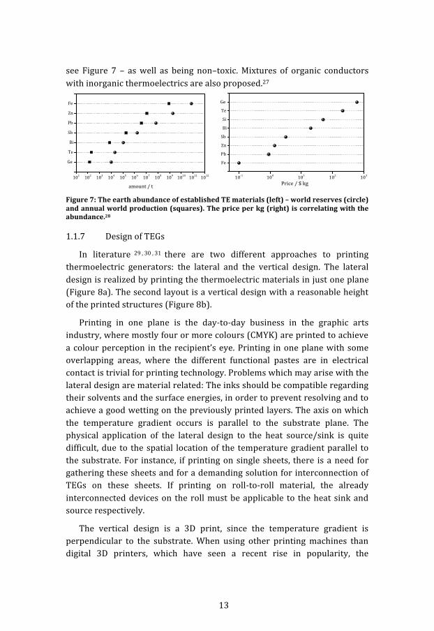
Organic conductors e.g. PEDOT, PANI and TTF-‐TCNQ25, 26 and the like have recently attracted renewed interest since they typically possess a very low thermal conductivity (0.3-‐0.8 Wm-‐1K-‐1) and a moderate electrical conductivity (up to 3000 S/cm).22 The abundance of the atomic elements used in organic conductors is another advantage over inorganic materials –
13
see Figure 7 – as well as being non–toxic. Mixtures of organic conductors with inorganic thermoelectrics are also proposed.27
Figure 7: The earth abundance of established TE materials (left) – world reserves (circle) and annual world production (squares). The price per kg (right) is correlating with the abundance.28
1.1.7 Design of TEGs
In literature 29 , 30 , 31 there are two different approaches to printing thermoelectric generators: the lateral and the vertical design. The lateral design is realized by printing the thermoelectric materials in just one plane (Figure 8a). The second layout is a vertical design with a reasonable height of the printed structures (Figure 8b).
Printing in one plane is the day-‐to-‐day business in the graphic arts industry, where mostly four or more colours (CMYK) are printed to achieve a colour perception in the recipient’s eye. Printing in one plane with some overlapping areas, where the different functional pastes are in electrical contact is trivial for printing technology. Problems which may arise with the lateral design are material related: The inks should be compatible regarding their solvents and the surface energies, in order to prevent resolving and to achieve a good wetting on the previously printed layers. The axis on which the temperature gradient occurs is parallel to the substrate plane. The physical application of the lateral design to the heat source/sink is quite difficult, due to the spatial location of the temperature gradient parallel to the substrate. For instance, if printing on single sheets, there is a need for gathering these sheets and for a demanding solution for interconnection of TEGs on these sheets. If printing on roll-‐to-‐roll material, the already interconnected devices on the roll must be applicable to the heat sink and source respectively.
The vertical design is a 3D print, since the temperature gradient is perpendicular to the substrate. When using other printing machines than digital 3D printers, which have seen a recent rise in popularity, the

14
implementation of thick layers is the domain of screen printing. Although ink layers up to several hundreds of microns are possible, the aspect ratio of height to width is an important criterion. Since this aspect ratio is limited by parameters of printing technology and the ink, several layers may be necessary in order to achieve the desired height of the printed structure. Thus, alignment is crucial as well as fast curing inks, while keeping the process time in mind. There are also graphic arts print products as well that require more than 20 print runs for a completely printed image. But with costs in mind, the process should be kept as easy as it can be to maintain the benefit of low cost manufacturing.
Figure 8: a) The lateral layout is printed in one plane, illustrated after Glatz30. The temperature gradient is parallel to the substrate. b) The vertical layout based on five layers. The temperature gradient is perpendicular to the substrate.
1.2 Screen Printing
Screen printing is the most important technology in the field of functional printing. Its importance derives from the versatility of the method: Almost every imaginable combination of ink and substrate is viable with screen printing. Beyond that, it is possible to transfer wet ink films on the substrate in a wide range – from below microns up to several hundreds of microns. The viscosity of the ink for screen printing could also be very different, depending on the deployed mesh geometry.
Thick film printing in screen printing mostly depends on the thickness of the fabric. The thread diameter and the weaving of the mesh govern the thickness of the fabric. A smaller contribution to the transferable wet ink film thickness is made by the stencil thickness. The theoretical ink volume Vth in cm3m-‐2 depends on the percentage of open mesh area α0, and the mesh thickness D. Figure 9 illustrates the theoretical ink Volume.
𝑉𝑉!! =𝛼𝛼!𝐷𝐷100
(13)
Vth is corresponding to wet ink deposit in μm.

15
Figure 9: The nomenclature of screenmeshes (left) and a sketch of theoretical ink volume Vth. Source: SEFAR® PA, Datasheet.
Since the total ink volume will not be released from the mesh, the true value of the wet ink thickness is 10 to 30 % less than calculated.32 The influence of the stencil must additionally be considered. Depending on the solid content of the inks, the dry ink thickness could be calculated. For instance, the wet ink thickness of PEDOT:PSS reduces massively, since the solid content is around 1 to 2 % only. The reduction of metal-‐filled inks is around 50 %.
Different stencil materials are available: liquid emulsion and direct as well as indirect film. Emulsions are made of UV-‐curing materials that are applied on the mesh by a coating trough (scoop coater). This could be done manually or automatically with an automatic screen coating machine. The indirect and direct films are based on PET films that were previously coated with photosensitive material in a continuous coating process. Both emulsion and films are usually exposed to UV light using a lithographic film. Direct films are applied on the screen mesh before exposure and development; indirect film is applied after the two process steps. Film can be applied by wetting the mesh with water so that the film will be partially sucked into the mesh (capillary film). Otherwise, it is possible to adhere the film with liquid emulsion to the mesh. This is necessary with thick films > 150 µm.
Different emulsions for manually or automatically screen coatings are available. They differ in the chemical reactants, the mechanical and chemical resistance and the viscosities. For many different applications there are specially designed emulsions on the market. Specific emulsions for thick film printing are available, but also capillary films are available in different thicknesses up to some hundreds of microns.
The advantage of using a capillary film is the well-‐defined thickness of the emulsion coated on the PET film. The continuously coated film also results in a small surface roughness (Rz) of the film. The roughness parameter Rz is obtained by the measurement instruction according to

16
Figure 10. It is therefore possible to have a very reproducible stencil on the screen. The drawbacks of the film are the weaker adhesion to the mesh and higher costs. The result is a shorter lifetime of a stencil made by film.
Figure 10: Ten-‐point mean roughness Rz. The absolute values of five samples in Yp and Yv direction are added and finally divided by five. Source: Excerpt from JIS B 0031 (1994)
1.2.1 Screen Preparation
Precise printing forms made of an aluminium frame, mesh (PET, PA or metal) and the stencil materials described in the sections above are crucial for high quality screens. The process of tensioning the screen is the first important step, especially if several layers are successively printed, which require best alignment quality. The mesh material and the thread count, for instance, determine the maximum tensioning value in Ncm-‐1. During the first 24 hours the screen tension degrades significantly (relaxation), such that an overhead must be taken into account.
The second step towards a high quality screen is, for instance, the reproducible and stable stencil created by coating with wet emulsion or by the application of capillary film. The latter is easily applied by wetting the screen. The applied capillary film will then be sucked into the mesh. The precise film thickness of the stencil and the low surface roughness are the benefits of this technique, and therefore the reproducibility is excellent.
The automatic coating of the screen also allows for reproducible results. Mesh structure compensation is an important issue of emulsion coating (compare Figure 11). The last coating stroke of wet-‐in-‐wet coating must be applied from the squeegee side of the screen, since the emulsion flows through the mesh from the squeegee side to the print side (the side facing towards the substrate). Several coating strokes may be necessary in order to compensate the mesh structure on the print side to achieve good print quality. Usually, the number of coatings on the squeegee side is higher than the coatings on the print side.

17
Figure 11: Effect of mesh coating on print quality: a) stencil too thin – saw tooth effect; b) correct stencil – sharp print; c) stencil too thick – unclear print.33
1.2.2 Imaging and Screen Development
Although digital imaging of printing plates is state of the art in every printing technology, screen printers often rely on lithographic film based imaging that may appear old fashioned. In fact, the quality of lithographic films is high and there are plenty of coating emulsions on the market for this kind of screen preparation. The lithographic film is placed with the light-‐blocking layer on the coated mesh. The imaging process itself is of course a potential source of errors; such as an undercut during exposition to UV light or an inappropriate quantity of UV light. For every material combination, i.e. mesh type, emulsion and exposure unit, there is an ideal range for the parameters, which have to be determined prior to screen preparation.
The development of the screen is less prone to errors, but in the case of thick film stencils, there are some issues with the process duration and the adhesion of the emulsion to the mesh.
1.2.3 Printing
Print results depend on the screen quality and the printing step itself. For multilayer prints, the alignment of the successively printed images, e.g. of the vertical TEG layout, is crucial. The precision of the printing machine, as well as the experience of its operator, are indispensable. An optical assistance system is beneficial for semi-‐automatic printing machines. Notwithstanding accuracy of alignment, the structures will most probably broaden with every additional print run. Broadening of structures by multilayer printing leads to reduction of the apertures in the insulating layer of the vertical design (Figure 8b, middle). Thus, the active area of the legs will decrease. As a result, the performance of the TEG will also be affected.

18
The parameters of the printing process are manifold. The most important parameters are: the squeegee speed, angle, pressure, material and shape, as well as the snap off distance. Printing machines differ in the mechanism of moving the screens away from the printing table. A parallel stroke movement is preferable.
1.3 Rheology
“Rheology describes the deformation of a body under the influence of stresses. 'Bodies' in this context can be either solids, liquids, or gases”.34 The term rheology was coined in the 1920s and derives from Greek aphorism ”panta rhei” meaning everything flows. This field of science gained more and more importance, since the rheological properties of materials are crucial for, amongst other things, industrial processes such as printing.
Materials can be classified according to their behaviour under stress, i.e. shear rate and shear stress. Liquids like water are ideal Newtonian fluids with shear rates proportional to shear stress, see Figure 12.
Figure 12: Classification of rheological behaviours. Printing inks are pseudoplastic fluids.35
Printing inks in general are pseudoplastic, i.e. shear thinning fluids. Dilatant fluids show the opposite behaviour of shear thickening. Many liquids are having both elastic and viscous properties, thus they are named viscoelastic fluids. The flow behaviour of printing inks is a key factor to high quality printing, since the inks need to fulfil several requirements before, during and after the printing process. In the scope of this thesis only the properties of screen printing inks are considered. One of the most important rheological parameters is the viscosity.

19
1.3.1 Viscosity
The resistance to flow is called viscosity and it is one of the most important rheological parameters not only of printing inks. The dynamic viscosity is a measure of the internal friction of a fluid and is determined from the quotient of shear stress and shear rate.
𝜂𝜂 =𝜏𝜏𝛾𝛾 (14)
with viscosity η in Pa•s, shear stress τ in Pa and shear rate 𝛾𝛾 in s-‐1.
Using a simple model, the shear rate and shear stress can be illustrated as follows: Two adjacent, parallel plates enclose a liquid, see Figure 13. By moving the top plate parallel to the bottom plate with the velocity 𝑣𝑣 of the shear force 𝐹𝐹, laminar shearing will take place in the liquid. The boundary layer beneath the top plate also moves with velocity 𝑣𝑣, while the boundary layer upon the bottom layer does not move at all. The liquid could be seen as being a huge number of infinitesimal thin laminar layers in between these two extreme values. All the layers have different velocities. A linear velocity gradient will be established.
Figure 13: A model illustrating the viscosity of fluids.
The shear stress is defined as the force 𝐹𝐹 applied on the cross-‐sectional area 𝐴𝐴 of the top plate in contact with the liquid
𝜏𝜏 =𝐹𝐹𝐴𝐴 (15)
The shear rate 𝛾𝛾 in s-‐1 is defined as
𝛾𝛾 =𝑣𝑣ℎ (16)
with velocity 𝑣𝑣 and the height ℎ.

20
1.3.2 Thixotropy
Pseudoplastic or shear-‐thinning behaviour describes the reduction of the viscosity while the shear rate increases. If there is a threshold shear rate, which must be exceeded in order to enable the material to flow, it is called yield stress, see yield point in Figure 12. Pseudoplastic materials are called thixotropic if their pseudoplasticity is time-‐dependent. In thixotropic materials, the viscosity decreases even at constant shear rates, see Figure 14. In the case that no more shear stress is applied the ink builds back, time-‐dependently, to the initial viscosity value.
Figure 14: Thixotropy is a required property of printing inks. The time-‐dependent relaxation and restoration of the initial viscosity is needed for a smooth surface of the printed image.
“Thixotropy is very important to proper ink behaviour and we can factually state that the changing viscosity attribute makes screen printing possible”.36 Thixotropic fluids show specific hysteresis curves depicting the time constant of restoring to the initial viscosity. A partially thixotropic liquid will not recover to the initial viscosity value.
1.3.3 Levelling
While printing, the mesh elongates with the squeegee stroke. The squeegee pushes the ink in the mesh openings. Behind the moving squeegee the mesh releases from the wet ink film on the substrate, leaving marks from the mesh. This effect is called mesh marking and depends, for example, on screen tension and squeegee speed.32 The equalization of a rough ink surface, such that a homogenous surface topology can be established, is called levelling. Printing inks are thixotropic fluids.
The recovery time that is needed for regaining the initial viscosity, as well as the lowest viscosity reached when shear stress stops – see dashed line in Figure 14 – determine the flow behaviour of the printed structure. The longer the recovery time is, the more the ink tends to bleed out. With
21
this in mind, it is advisable to aim for a short recovery time, in order to obtain high edge definition. However, if a smooth surface topology of the printed structure is important, the ink release from the mesh and the levelling of the wet ink must also be considered.
While the flow of the ink is needed for a smooth surface, it is undesirable with regard to the edge definition. Surface levelling and precise edge definition are contradictory requirements. Both are reliant upon the time depending restoration of the viscosity (thixotropy). A too short levelling time results in meshmarking in the dry ink film surface. A too long levelling time will lead to an unwanted broadening of the printed structure.
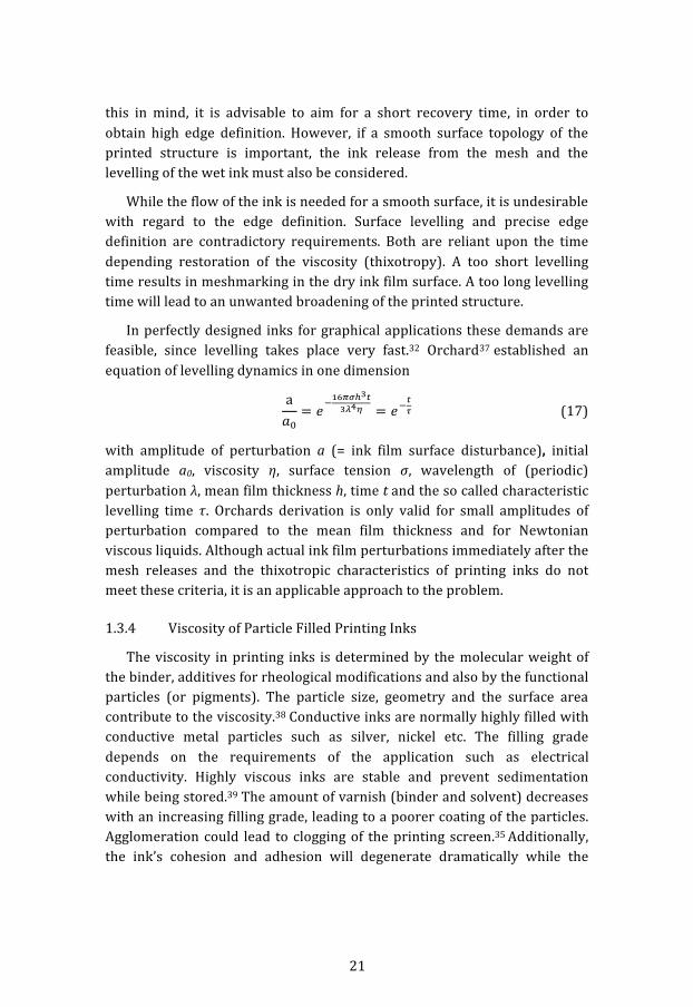
In perfectly designed inks for graphical applications these demands are feasible, since levelling takes place very fast.32 Orchard37 established an equation of levelling dynamics in one dimension
a𝑎𝑎!= 𝑒𝑒!
!"!"!!!!!!! = 𝑒𝑒!
!! (17)
with amplitude of perturbation a (= ink film surface disturbance), initial amplitude a0, viscosity η, surface tension σ, wavelength of (periodic) perturbation λ, mean film thickness h, time t and the so called characteristic levelling time τ. Orchards derivation is only valid for small amplitudes of perturbation compared to the mean film thickness and for Newtonian viscous liquids. Although actual ink film perturbations immediately after the mesh releases and the thixotropic characteristics of printing inks do not meet these criteria, it is an applicable approach to the problem.
1.3.4 Viscosity of Particle Filled Printing Inks
The viscosity in printing inks is determined by the molecular weight of the binder, additives for rheological modifications and also by the functional particles (or pigments). The particle size, geometry and the surface area contribute to the viscosity.38 Conductive inks are normally highly filled with conductive metal particles such as silver, nickel etc. The filling grade depends on the requirements of the application such as electrical conductivity. Highly viscous inks are stable and prevent sedimentation while being stored.39 The amount of varnish (binder and solvent) decreases with an increasing filling grade, leading to a poorer coating of the particles. Agglomeration could lead to clogging of the printing screen.35 Additionally, the ink’s cohesion and adhesion will degenerate dramatically while the

22
viscosity will simultaneously rise. Heavily filled inks behave more like slurries than printing inks.
The viscosity of screen printing inks or pastes ranges between rather low to high values. Thinner inks may start at η=1 Pa•s, thicker pastes are more viscous with up to around η=20 Pa•s.
The optimized viscosity for screen printing is dependent on the printing parameters. If circumstances are changing, such as the ambient temperature and humidity level, or parameters are changed, e.g. printing velocity, squeegee to screen angle, squeegee pressure etc., the quality of the printed image will be influenced. Adjustment in the paste viscosity for any particular screen printing set up can only be fully optimised by experiment. Screen printers often use thickening agents, solvent blends and retarders for modifying the flow behaviour of the inks. A low viscosity may be the reason for printed lines tending to bleed out. On the other hand, if the printed structures show mesh marking or pinholes, it is likely that the paste viscosity is too high.40
23
2 Printing Inks and Substrates In this section, the materials used for printing thermoelectric generators
are discussed. The main focus lies on the thermoelectric materials, since there are no commercial products available. Secondly, the insulating material is crucial in order to establish a high thickness of the thermoelectric device. The material research in thermoelectrics is a vivid process. Researchers examine and create many different classes of materials with the goal of achieving good thermoelectric properties, while maintaining low toxicity and a high natural abundance. Most of the conventional thermoelectric materials are inorganic conductors, which do not meet these latter requirements. The design of efficient organic TE materials would be a dream for researchers due to their low costs, easy processing, environmental friendliness, low weight and their abundance.41
Using printing methods as the process to establish thermoelectric legs from unsoluble inorganic or organic material is a challenge. The first important requirement to be met is to provide the functional particles in printable ink. Furthermore, the ink has to match the required rheological properties depending on the used printing method. The thixotropic reformation of the ink after being transferred onto the substrate is a key factor, as well as the viscosity of the ink. The second important and most challenging requirement is that the electrical and thermoelectrical properties of the dried ink or sintered ink are as close as possible to the ideal bulk properties of the thermoelectric material.
2.1 Metal-‐Filled Functional Printing Inks
There are several different systems of functional printing inks aiming towards different fields of application. The desired functionality is most often the electrical conductivity or resistivity. Inks containing silver are deployed for good electrical conductivity requirements. Carbon-‐black inks are on the other hand used for generating (high) resistances. Several other metal pigments and blends are used for special applications such as Pd, Ag/AgCl, Ni, AgPd etc. Not only the pigment material is a specific property of the inks, also the binder and the solvents are selected due to the very specific requirements. Functional inks containing electrically conducting pigments can be divided into polymer thick film pastes (PTF), ceramic thick film pastes (CTF) and solder pastes. Here, the terms pastes and inks are interchangeable since conductive inks are mostly highly filled with functional pigments, thus leading to high viscosity ink, i.e. a paste.

24
The three types of conducting inks (PTF, CTF and solder pastes) contain a polymer binder to ensure the processability of the ink. The difference is that for the first group (PTF), the polymer will be part of the final dry ink, while for the CTF and solder pastes the polymer binder is burned out while heating up the printed specimen. Therefore, PTF pastes are called low temperature inks (max. of ~200°C), while the other two groups could be fired up as high as 1000°C and more, depending on the deployed binder system. A maximum processing temperature of around 150°C is crucial for applications on cheap flexible substrates such as PET and the like. Only low temperature PTF pastes are capable of curing in that temperature range.
2.1.1 Thermoplastic and Thermosetting Binders
The binders of PTF pastes consist of either thermoplastic or thermosetting polymers. The two material classes differ in their response to thermal treatment. While thermoplastics can be reversibly remolten, thermosets are stable against heating until thermal decomposition takes place. Thermoplastics exhibit linear or branched chains. The van der Waals bonds between the thermoplastic molecules are weaker than the crosslinks between the polymer chains occurring in thermosetting polymers. By applying heat, the long polymer chains in thermoplastics are no longer bound to the adjacent polymerchains. The thermal energy is sufficient to overcome the weak van der Waals forces. The polymer chains can slide past each other. The material behaves reversely by cooling.42
Figure 15: Schematic molecular configurations of (a) a thermoplastic and (b) a thermosetting polymer.43
The crosslinks between the long molecular chains of thermosetting polymer are strong chemical bonds that form a three-‐dimensional network, as depicted in Figure 15. This network is rigid and stiff, thus, the polymerchains hardly move while being heated.
Schematic molecular configurations of (a) a thermoplasticand (b) a thermoset

25
2.1.2 Conduction Mechanism
The conductivity in metal-‐filled polymer pastes depends directly on the filling grade of the conductive pigments. If the so-‐called percolation threshold is not met, the conductivity of the paste will be very low, or even nonexistent. The percolation threshold marks the amount of particles in the polymer matrix that is necessary to establish electrical pathways, as shown in Figure 16.
If the electrical conduction between conductive particles is limited either by the presence of an oxide coating or the small contact area between particles, the volume resistivity of the composite material is governed by the resistivity of the insulating binder. At low filling grade the particles are not in contact, but if the distance is small enough and the oxide thin enough, tunneling between the particles is possible, i.e. there is low electrical conductivity. At the percolation threshold or critical concentration, the resistivity reduces dramatically due to the contact between the particles.44
The electrical conductivity of bulk metals will never be achieved by low temperature curing printing inks containing metal pigments. There is a big difference between thermal treatment in order to remove residual solvents from the printed structures and sintering of the metal particles. Sintering normally takes place in higher temperature ranges when using CTF pastes. With nanoparticles it is already possible to achieve sintering of the pigments already in the low-‐temperature domain below 200°C.
Figure 16: Illustration of the percolation threshold. When the critical concentration is reached, the resistivity drops dramatically.45
26
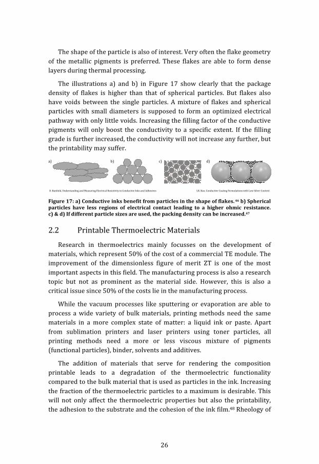
The shape of the particle is also of interest. Very often the flake geometry of the metallic pigments is preferred. These flakes are able to form dense layers during thermal processing.
The illustrations a) and b) in Figure 17 show clearly that the package density of flakes is higher than that of spherical particles. But flakes also have voids between the single particles. A mixture of flakes and spherical particles with small diameters is supposed to form an optimized electrical pathway with only little voids. Increasing the filling factor of the conductive pigments will only boost the conductivity to a specific extent. If the filling grade is further increased, the conductivity will not increase any further, but the printability may suffer.
Figure 17: a) Conductive inks benefit from particles in the shape of flakes. 46 b) Spherical particles have less regions of electrical contact leading to a higher ohmic resistance. c) & d) If different particle sizes are used, the packing density can be increased.47
2.2 Printable Thermoelectric Materials
Research in thermoelectrics mainly focusses on the development of materials, which represent 50% of the cost of a commercial TE module. The improvement of the dimensionless figure of merit ZT is one of the most important aspects in this field. The manufacturing process is also a research topic but not as prominent as the material side. However, this is also a critical issue since 50% of the costs lie in the manufacturing process.
While the vacuum processes like sputtering or evaporation are able to process a wide variety of bulk materials, printing methods need the same materials in a more complex state of matter: a liquid ink or paste. Apart from sublimation printers and laser printers using toner particles, all printing methods need a more or less viscous mixture of pigments (functional particles), binder, solvents and additives.
The addition of materials that serve for rendering the composition printable leads to a degradation of the thermoelectric functionality compared to the bulk material that is used as particles in the ink. Increasing the fraction of the thermoelectric particles to a maximum is desirable. This will not only affect the thermoelectric properties but also the printability, the adhesion to the substrate and the cohesion of the ink film.48 Rheology of

27
massively filled metal-‐pigment inks differs significantly from lower filled inks.
2.2.1 Bi and Sb Containing Printing Inks
Bismuth is the most promising thermoelectric material in conventionally produced thermoelectric generators in the temperature range below 200°C. An alloy of Bi and Te is widely used both in thermoelectric generators and in Peltier devices. Sb also shows a considerable high Seebeck coefficient. From the process perspective all the aforementioned materials are lacking in compatibility with already existing ink formulations (binder-‐solvent matrices) established for low temperature metal-‐filled polymer inks. Like other metal particles that are not usable for low temperature printing inks due to their tendency to oxidize, Bi2Te3 as well as Bi and Sb are similar to Al, Cu and the like. Printing inks consisting of these particles may be available, but not in the low temperature regime 49, 50 or only in combination with more complex treatment processes after printing such as photonic sintering.51 Other printing methods are utilized52, 53, so that the ink does not have to meet the rheological requirements of screen printing. Additionally, the abundance of these materials is low but the toxicity is rather high – two attributes that, beside their modest thermoelectric efficiencies, are obstructive for a mass application of printed thermoelectric generators based on Bi and Te. Sb is also considered to be amongst a list of critical raw materials “due to their high relative economic importance and to high relative supply risk”. 54 Nonetheless, some research institutes are looking into methods as to how to apply Bi, Te or Sb containing inks on flexible substrates in the higher49, as well as lower temperature range. 29, 55
2.2.2 Nickel Printing Inks
In the manufacturing of printed circuit boards (PCB) and electronics, nickel is one of the important metals to pattern conductive tracks. Usually, the base material of a PCB is copper, which is prone to oxidation. A gold layer is used to protect the traces and contacts from corrosion. A diffusion barrier consisting of a Ni layer between the Cu and Au layer provides long-‐term stability of the traces and contacts. Although nickel is widely used in electronics, it is a toxic allergen suspected of causing cancer and this may be why many manufacturers of Ni printing inks withdrew their products in the past. Ni ink is still available from only a few manufacturers (Creative Materials Inc., Gwent Group, DuPont).

28
Metallic Ni oxidizes slower than Cu and Al for example, hence there is no need for inert atmospheres during the mixing of the ink. Dispersing the particles is therefore rather simple, since no sophisticated laboratory equipment is necessary. Due to the poor malleability, the Ni particles cannot be forged in flakes. Thus, Ni inks have lower conductivity than Ag inks. However, Ni inks are used in shielding applications, as well as in conductive adhesives anisotropical and isotropical ink systems. 56
2.2.3 Conducting Polymers
Traditionally, polymers (poly = many, mer = unit) are valued for their chemical, mechanical and electrical resistance. But since the discovery of intrinsic electrically conductive polymers in the seventies and the possibility of doping (in chemical terms: oxidation and reduction), conducting polymers found interest in many new applications, such as optoelectronics, printed electronics, supercapacitors, microactuators, etc. 57 This class of material combines unique features, such as solution processibility, lightweight, flexibility, optical and electrical properties. Because of the ground nature of this discovery, A. Heeger, A. Mc Diarmid and H. Shirakawa were awarded the Nobel Prize in Chemistry in 2000. Polymer electronics is also named organic electronics, since carbon is the backbone of conducting polymers.
Figure 18: Electron configuration of carbon atoms. From left: ground state, sp3-‐ and sp2-‐hybridizations.
In the early valence bond theory, bonds in molecules were explained from the atomic electronic structure and the notion of hybrid orbitals. The electronic configuration of the carbon atom in its ground state is: 1s22s2px1py1, i.e. two electrons are able to form covalent bonds (tetravalent). In order to explain that in methane carbon has four bonds, one introduced the notion of “promotion”. That is, assume that electrons can be excited and occupy higher energy level. The energy cost of this excitation will be balanced by the stabilization energy due to the creation of several bonds
oundst

29
using those excited electrons. A modification of the ground state is necessary to have four half-‐filled orbitals.
If one electron from the 2s-‐orbital is elevated into the pz-‐orbital, the carbon atom is in an excited state with the configuration 1s22s1px1py1pz1. In this excited state, four covalent bonds are possible. Since there are three half-‐filled p-‐orbitals and one s-‐orbital, the bonds would not be identical. However, one can consider instead that four new hybridized orbitals named sp3 will be established as linear superpositions between the 2s-‐orbital and the three p-‐orbitals. With this notion of hybrid orbitals, the four identical bonds in methane are rationalized.
The energies of the sp3-‐orbitals are lower than that of the p-‐orbitals, but higher than that of the 2s-‐orbital, since three p-‐orbitals and one s-‐orbital contribute energetically to the hybrid-‐orbital. Additionally, there are sp2-‐ and sp-‐hybridization (1s22sp3p1 and 1s22sp2p2, respectively) to the sp3-‐hybrid (1s2sp3).
2.2.3.1 Conjugated Polymers
In conjugated polymers (CP), the carbon atoms are sp2-‐hybridized. The sp2-‐orbitals of each carbon atom are sitting in one plane forming σ-‐bonds with three sp2-‐orbitals of adjacent atoms. The two-‐lobe shaped pz-‐orbital is perpendicular to the plane formed by the sp2-‐orbitals of each atom. The electrons in pz-‐orbitals of adjacent carbon atoms are able to form π-‐bonds. Hence there is a double bond (π-‐ and σ-‐bond) between the two carbon atoms, see Figure 19. Conjugated polymers are characterized by an alternation between single and double bonds along the chains of carbon atoms. Sometimes other atoms such as oxygen, sulphur or nitrogen atoms are involved in the conjugated paths.
Figure 19: A sketch of alternating double and single bonds. For each C-‐atom the pz-‐orbital is perpendicular to three sp2-‐ortbitals that are in one plane (120°). The pz-‐orbitals of adjacent atoms are overlapping in π-‐orbitals forming a π-‐bond besides the σ-‐bond.
30
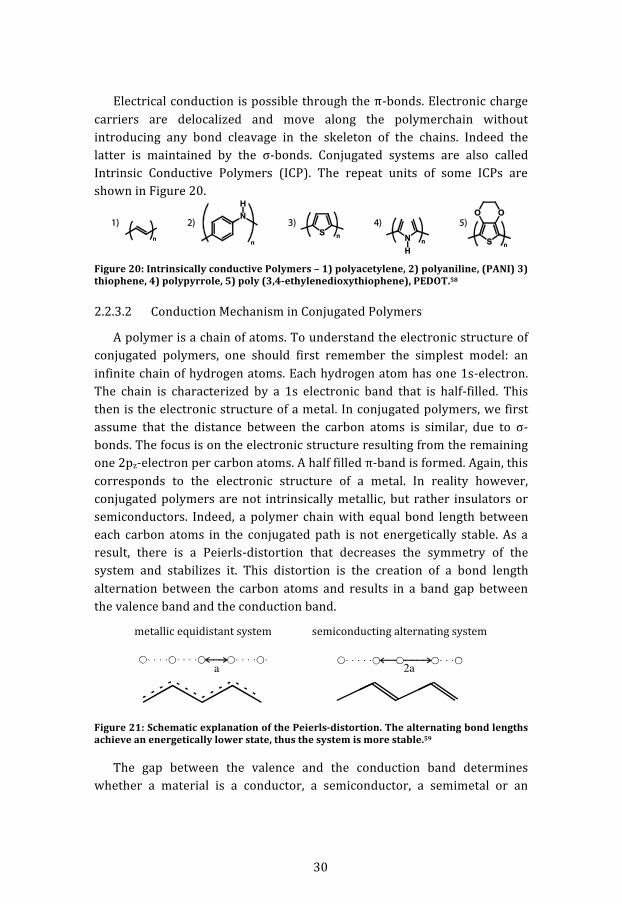
Electrical conduction is possible through the π-‐bonds. Electronic charge carriers are delocalized and move along the polymerchain without introducing any bond cleavage in the skeleton of the chains. Indeed the latter is maintained by the σ-‐bonds. Conjugated systems are also called Intrinsic Conductive Polymers (ICP). The repeat units of some ICPs are shown in Figure 20.
Figure 20: Intrinsically conductive Polymers – 1) polyacetylene, 2) polyaniline, (PANI) 3) thiophene, 4) polypyrrole, 5) poly (3,4-‐ethylenedioxythiophene), PEDOT.58
2.2.3.2 Conduction Mechanism in Conjugated Polymers
A polymer is a chain of atoms. To understand the electronic structure of conjugated polymers, one should first remember the simplest model: an infinite chain of hydrogen atoms. Each hydrogen atom has one 1s-‐electron. The chain is characterized by a 1s electronic band that is half-‐filled. This then is the electronic structure of a metal. In conjugated polymers, we first assume that the distance between the carbon atoms is similar, due to σ-‐bonds. The focus is on the electronic structure resulting from the remaining one 2pz-‐electron per carbon atoms. A half filled π-‐band is formed. Again, this corresponds to the electronic structure of a metal. In reality however, conjugated polymers are not intrinsically metallic, but rather insulators or semiconductors. Indeed, a polymer chain with equal bond length between each carbon atoms in the conjugated path is not energetically stable. As a result, there is a Peierls-‐distortion that decreases the symmetry of the system and stabilizes it. This distortion is the creation of a bond length alternation between the carbon atoms and results in a band gap between the valence band and the conduction band.
Figure 21: Schematic explanation of the Peierls-‐distortion. The alternating bond lengths achieve an energetically lower state, thus the system is more stable.59
The gap between the valence and the conduction band determines whether a material is a conductor, a semiconductor, a semimetal or an
a 2a

31
insulator. In the case of organic conductors the highest occupied molecular orbital (HOMO) is the upper edge of the valence band. Accordingly, the lowest unoccupied molecular orbital (LUMO) is the lower edge of the conduction band. Organic semiconductors also have a band gap between the HOMO and LUMO, similar to inorganic semiconductors. With increasing conjugation length, the band gap decreases.
2.2.3.3 Doping of Conjugated Polymers
Chemical Doping
In its pristine form, the electrical conductivity of conjugated polymers is close to those of traditional insulators. But when the polymer is oxidized (p-‐doped), the charge carrier density increases and the materials become an electrical conductor. Analogous to inorganic semiconductors, the doped charges result in gap states.57 The doped charges are not only a charge in excess on the polymer chain, but they are also associated with a localized distortion on the polymer chain, i.e. the structure in the proximity of the doped charge is distorted. The charges with a local relaxation are forming quasiparticles. These charged quasiparticles could be called solitons, polarons and bipolarons, depending on their characteristics.60 Solitons only exist in degenerate ground state CPs, like polyacetylene, in which the interchange of single-‐ and double bonds does not affect the energy of the polymer. In non-‐degenerate ground state polymers there are polarons and bipolarons. Polarons or bipolarons (higher concentration) are created, depending on the concentration of charge carriers added to the CPs.

32
Figure 22: Energy level diagrams of conductive polymers. “Dashed arrows indicate possible electronic transitions caused by light absorption.”61
The longer the conjugation length and the higher the doping level of the CP, the more localized states exists in the band gap, creating a band. In Figure 22 the energy levels of polarons and bipolarons in CP are illustrated.
Electrochemical Doping
It is also possible to carry out the redox reaction (doping) electro–chemically. Either a two-‐electrode set-‐up with a working and a counter electrode or a three-‐electrode set-‐up with an additional reference electrode is used for electrochemical doping. The three electrodes allow for precise monitoring and controlling of the electrochemical parameters.
With electrochemical doping, the doping level can be adjusted accurately by controlling the electrical current. This process is highly reversible, i.e. doping and dedoping is possible without removing chemical products.62, 63 As with chemical doping, a counter ion is also required with electrochemical doping, in order to stabilize the charge along the polymer backbone.62
Photo Doping
Photo doping is the effect of significantly increasing the electrical conductivity of a polymer by irradiation. Doping occurs when the radiation energy is greater than the band gap of the polymer. It is a volatile effect, since the recombination of free electrons and holes takes place rapidly and the creation of free electrons stops when irradiation stops64, but “the application of an appropriate potential during irradiation could separate
33
electrons from holes, leading to photoconductivity.”62 With photo doping there are no counter ions.
Charge-‐injection Doping
Charge carriers can “be injected into the band gap of conjugated polymers by applying an appropriate potential on the metal/insulator/polymer multilayer structure”64, analogous to the function of a field effect transistor (FET) or organic FET (OFET). Like photo doping, charge-‐injection doping is a volatile process that generates no counter ions.
Non-‐redox Doping
In contrast to the aforementioned ways of doping, the number of electrons associated to the polymer backbone do not change when applying the non-‐redox doping route. “The most studied doping process of this type is the protonic doping of polyaniline emeraldine base (PANI-‐EB) with aqueous protonic acids, such as HCl.”62 With non-‐redox doping “the conductivity is increased by a nine to ten order of magnitude.”64
Secondary Doping
Primary doping of conducting polymers changes the material properties, amongst others the electrical conductivity. By removing the dopant also the changes in material properties will vanish. If a second dopant is used supplementary to the first dopant, the material properties are further modified. Although the impact of the secondary dopant is smaller than of the primary dopant, the modification of the secondary dopant may be persistent even when it is removed.65 In the case of polyaniline, secondary doping leads to crystallinity even in the dispersion as well as in the solid polymer film. On the other hand, PEDOT:PSS films stay amorphous using secondary dopants and the effect of the secondary dopant only applies to the conformation of the polymer film when it already has been formed.66
34
2.3 Insulators and Substrates
Non-‐Conducting Polymers (NCPs) are used for dielectrics (insulators) and as substrates. NCPs are saturated polymers, i.e. all electrons are bound in σ-‐bonds. The band gap of NCPs is wide, such that there is no electrical conduction.
2.3.1 Printable Dielectrics
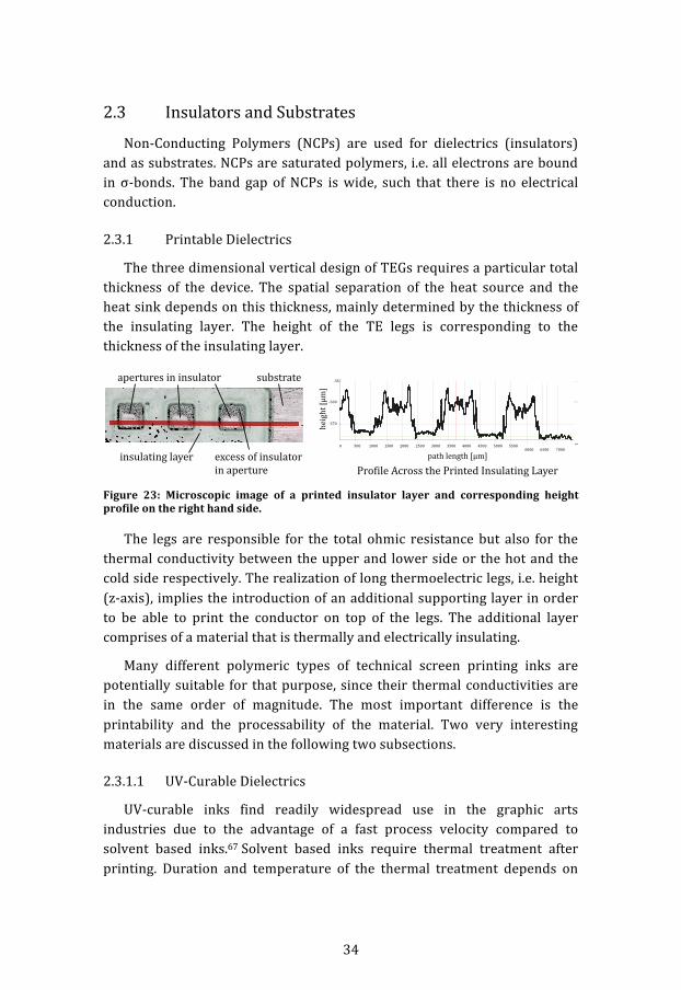
The three dimensional vertical design of TEGs requires a particular total thickness of the device. The spatial separation of the heat source and the heat sink depends on this thickness, mainly determined by the thickness of the insulating layer. The height of the TE legs is corresponding to the thickness of the insulating layer.
Figure 23: Microscopic image of a printed insulator layer and corresponding height profile on the right hand side.
The legs are responsible for the total ohmic resistance but also for the thermal conductivity between the upper and lower side or the hot and the cold side respectively. The realization of long thermoelectric legs, i.e. height (z-‐axis), implies the introduction of an additional supporting layer in order to be able to print the conductor on top of the legs. The additional layer comprises of a material that is thermally and electrically insulating.
Many different polymeric types of technical screen printing inks are potentially suitable for that purpose, since their thermal conductivities are in the same order of magnitude. The most important difference is the printability and the processability of the material. Two very interesting materials are discussed in the following two subsections.
2.3.1.1 UV-‐Curable Dielectrics
UV-‐curable inks find readily widespread use in the graphic arts industries due to the advantage of a fast process velocity compared to solvent based inks.67 Solvent based inks require thermal treatment after printing. Duration and temperature of the thermal treatment depends on

35
the evaporation time of the used solvents and the thickness of the ink film. The curing time of UV-‐cured inks is drastically lower. This enables a faster process, e.g. successively printed multilayer designs in a shorter period of time. Other benefits of UV inks are the reduction of volatile organic compounds (VOC), the lower energy consumption, no clogging in the stencil apertures and the stacking of the printed substrates without blocking, to mention just a few.68
'Drying' of UV inks is initiated and performed by chemical reactions of the radicals provided by the photoinitiators and the prepolymers/oligomers combining to a longchain polymer. It is therefore named polymerization or curing instead of the (physical) drying of solvent-‐based inks. Two principles of polymerization are mainly used in printing inks: the cationic and the radical polymerization.
Radical Polymerization
The constituents of UV inks are acrylate oligomers (responsible for the adhesion, mechanical resistance and flexibility of the ink film69) and acrylate monomers (added for setting the viscosity). Various additives are used for adjusting the thixotropy, surface wetting, stability against sedimentation, etc. Eventually, the photoinitiators are the most prominent part of a UV ink, since they provide the free radicals for the polymerization reaction induced by irradiation with light of a specific wavelength.
The photoinitiators split by absorbing the energy of the UV irradiation into free radicals that are unsaturated. These radicals are now able to crosslink the oligomers forming longchain thermosetting polymers (polymerization) that are stable against solvents and heat (unmeltable, see 2.1.1 Thermoplastic and Thermosetting Binders).
Figure 24: Steps of UV-‐curing. The wet ink is stable until UV irradiation. The photoinitiators, activated by the UV energy, split in free radicals and force the polymerization of the oligomers and monomers to longchain polymers.67
The photoinitiator I decomposes by irradiation. The free radicals have unpaired electrons that are able to bond with e.g. the monomers M. This process repeats until termination (reaction of radical with initiator radical
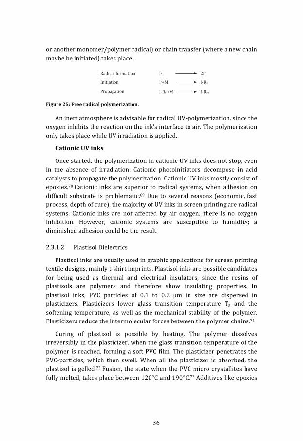
36
or another monomer/polymer radical) or chain transfer (where a new chain maybe be initiated) takes place.
Figure 25: Free radical polymerization.
An inert atmosphere is advisable for radical UV-‐polymerization, since the oxygen inhibits the reaction on the ink’s interface to air. The polymerization only takes place while UV irradiation is applied.
Cationic UV inks
Once started, the polymerization in cationic UV inks does not stop, even in the absence of irradiation. Cationic photoinitiators decompose in acid catalysts to propagate the polymerization. Cationic UV inks mostly consist of epoxies.70 Cationic inks are superior to radical systems, when adhesion on difficult substrate is problematic.69 Due to several reasons (economic, fast process, depth of cure), the majority of UV inks in screen printing are radical systems. Cationic inks are not affected by air oxygen; there is no oxygen inhibition. However, cationic systems are susceptible to humidity; a diminished adhesion could be the result.
2.3.1.2 Plastisol Dielectrics
Plastisol inks are usually used in graphic applications for screen printing textile designs, mainly t-‐shirt imprints. Plastisol inks are possible candidates for being used as thermal and electrical insulators, since the resins of plastisols are polymers and therefore show insulating properties. In plastisol inks, PVC particles of 0.1 to 0.2 µm in size are dispersed in plasticizers. Plasticizers lower glass transition temperature Tg and the softening temperature, as well as the mechanical stability of the polymer. Plasticizers reduce the intermolecular forces between the polymer chains.71
Curing of plastisol is possible by heating. The polymer dissolves irreversibly in the plasticizer, when the glass transition temperature of the polymer is reached, forming a soft PVC film. The plasticizer penetrates the PVC-‐particles, which then swell. When all the plasticizer is absorbed, the plastisol is gelled.72 Fusion, the state when the PVC micro crystallites have fully melted, takes place between 120°C and 190°C.73 Additives like epoxies

37
are used for improving the resistance to heat. Plastisol inks are inexpensive and show high adhesion and durability on several substrates.74
2.3.2 Flexible Substrates
The mass application of TEGs in waste heat environments implies the usage of cheap and flexible substrates. A good thermal conductor is needed, for a small thermal resistance at the interface between the heat source and the flexible TEG. Polymers are cheap materials (e.g. PE, PP or PET plastic foils) but poor thermal conductors. Compound films consisting of polymers and metallic foils like Al and Cu force a trade-‐off between flexibility, thermal conductivity and low costs. Usually a sandwich of polymer-‐metal-‐polymer is necessary in order to provide thermal stability, i.e. compensation of the coefficient of thermal expansion (CTE) mismatch. Such foils are usually made of Al or Cu films sandwiched by a polymer film such as polyethylene and polypropylene. These polymers are cheap but suffer from low maximum processing temperature. Polyethylene terephthalate (PET) provides an increased maximum processing temperature of 150°C. Expensive polyimide or polyamide substrates are necessary for higher temperature applications. The CTE is an important parameter in compound systems, since a thermal mismatch leads to problems in the processing of the substrate. In a roll-‐to-‐roll process, this mismatch could be negligible. Sheet-‐fed machines are very often used in the first trials, so that a CTE mismatch causes severe problems during thermal treatment of the specimen.
Another approach to the substrate configuration could be the usage of a bulk Al or Cu foil and a partially printed thin layer of an electrical insulator covering the areas where the bottom conductor of the TEG is successively printed on. Depending on the foil thickness – the metal layer in a compound foil is around 12 to 25 µm thick – a single Al foil is more difficult to handle than a compound foil due to the reduced stiffness. The film thickness of pure Al foils must be higher than that of a compound foil, thus increasing the costs. An advantage of a partially printed metal foil is the possibility of reducing the electrical insulating layer to a minimum, which leads in turn to a reduced minimum thermal resistance.
38
3 Experimental Setup All meshes were purchased from SEFAR, Switzerland. The wet emulsions
were obtained from Kissel + Wolf, Germany. The capillary films were obtained from the German distributor of Ulano. Silver, carbon-‐black and UV-‐dielectric inks were purchased from Acheson (Henkel), as well as from Sun Chemical. Ni, Sb and Bi particles were obtained from alfa-‐aesar.
Mixing of inks was performed using an ultraturrax and a dissolver. The particles were milled with a vibrating tube mill. All samples were printed on an AsysEkra X-‐1 stencil/screen printing machine. A technigraf continuous furnace UV-‐curing unit was used for the insulating layer. The specimens were dried in a Binder batch-‐furnace.
39
4 Conclusion of the Published Papers There are at least three different disciplines to consider when
approaching the problem “Screen printing of Thermoelectric Devices”. Knowledge about thermoelectricity and the design of such devices is needed first, in order to establish a process for a printing technology. TE materials have to be matched to the printing process and the simulation of the (print) production is a desirable tool.
Optimization of screen preparation
The first paper addresses the optimization of the screen preparation for thick film printing. The prominent layer in the vertical design of printed TEGs is the insulating layer. This layer determines the length and the area of the thermoelectric legs, hence the active area of the TEG. Knowledge of the crucial parameters in screen printing is necessary to avoid shortcomings in the printed structures regarding the performance of the TEG. The most important parameters in screen preparation were identified.
Examination of several Ni-‐ink formulations
In Paper 2 modifications of the initial Ni-‐ink formulation was driven by the need for optimized rheological properties, namely the filling of deep cavities and the building of a homogenous surface topology. An initial Ni-‐ink formulation was modified with rheology additives. It was found that the additives altered the rheological but also more drastically the electrical conductivity of the inks. Only few specimens were found to be better than the initial formulation, since electrical conductivity is the first and most important criterion. The “doughnut effect” – spherical shaped reduction in height in the middle of the filled up cavity – was reduced. It was also found that stencil printing is superior to screen printing in this regard. This may relate to the mean particle sizes and the distribution thereof, since the highly filled Ni-‐inks tend to clog the screen mesh.
Modelling a (Printed) TEG
The dependency of the geometric dimensions and the performance of a printed TEG including thermal parameters were examined in the third paper. Two approaches were realized: starting with the given materials and geometric parameters, upon which the thermoelectric parameters as voltage and electric power could be calculated. The second approach was to adapt the parameters to requirements as given load, needed voltage and power.

40
5 Goal of the Thesis With this thesis the author investigated screen printing of thermoelectric
generators as a possible production process. Others have already shown the feasibility of printed TEGs, but mostly only the lateral design was investigated.
The projects concluded in this thesis were exclusively aimed towards a printing process for vertical (3D) TEG-‐layouts. The main difference of both designs is the separation of the heat source and heat sink. While it is very easy to print long lateral structures providing a spatial separation of the heat source and sink, the internal resistance of the TEG suffers from the low electrical conductivity of the thermoelectric materials used for the legs. A high total resistance of the TEG leads to a low power delivered by the generator. If the length of the legs is reduced such as with the vertical design, the total resistance is smaller.
The challenge of the vertical design is the separation of the heat sink and source in order to maintain the temperature difference that provides the functionality of the whole device. Initial tests showed that the vertical design is feasible when using screen printing for all layers.
The optimization of the printing technology is necessary in order to achieve a thick ink layer and thus an overall thickness of the thermoelectric device that provides a persistent temperature gradient. Material science and thermoelectric fundamentals are the basis of the creation of thermoelectric pastes that could be applied in screen printing.
The inks used for the establishment of a fully printed vertical thermoelectric generator need further development. TE materials with higher Seebeck coefficients with reduced oxidation tendency in a liquid matrix are needed. The first step towards all screen printable 3D TEGs has been taken, but many efforts must be made in the future to develop a manufacturing process which is able to produce printed TEGs on a large scale.
41
6 References
1 Goldsmid HJ. Introduction to Thermoelectricity. Springer; 2009. 2 Vining CB. An inconvenient truth about thermoelectrics. Nat Mater. 2009. 3 Schneider M et al. World Nuclear Industry Status Report 2013. 2013. 4 Holmberg K et al. Global energy consumption due to friction in passenger cars. Tribology
International. 2012. 5 Carlson EJ et al. A 20 mV Input Boost Converter With Efficient Digital Control for
Thermoelectric Energy Harvesting. IEEE J. Solid-‐State Circuits. 2010. 6 Yazawa K, Shakouri A. Cost-‐efficiency trade-‐off and the design of thermoelectric power
generators. Env. Sci. Tech. 2011. 7 Abelson RD et al., Expanding Frontiers with Standard Radioisotope Power Systems. January
12. 2005. 8 Jänsch D. Thermoelektrik, eine Chance für die Automobilindustrie; mit 23 Tabellen. expert
verlag; 2009. 9 Kasap S. Thermoelectric effects in metals: thermocouples. 2001. 10 Spanner DC. The Peltier Effect and its Use in the Measurement of Suction Pressure. J. Exp.
Bot. 1951. 11 Czichos H. Hutte. 1989. 12 Rowe DM. Modules, Systems, and Applications in Thermoelectrics. CRC Press. 2012. 13 Snyder GJ. Small thermoelectric generators, Electrochem. Soc. Interface 2008. 14 Rowe DM. Themoelctric wasteheat recovery as renewable energy. Int. J. of Innov. in Energy
Sys. and Power 2006. 15 Sommerlatte J. Thermoelektrische Multitalente, Physik-‐Journal 6. 2007. 16 Snyder GJ, Toberer ES. Complex thermoelectric materials. Nat. Mater. 2008. 17 Zheng J. Recent advances on thermoelectric materials. Front. Phys. China. 2008. 18 Zuev YM et al. Diameter dependence of the transport properties of antimony telluride
nanowires. Nano Lett. 2010. 19 Zhigal'skii G, Jones BK. The Physical Properties of Thin Metal Films. CRC Press. 2003. 20 Sigrist M. Solid State Theory, lecture notes, spring semester ETH Zürich. 2013. 21 Ohtaki M. Oxide Thermoelectric Materials for Heat-‐to-‐electricity Direct Energy Conversion.
Novel Carbon Resources Sciences Newsletter Vol. 3. 2010. 22 Bubnova O et al. Semi-‐metallic polymers. Nat. Mater. 2013. 23 Wood C. Materials for thermoelectric energy conversion. Rep. Prog. Phys. 1988. 24 Wan C et al. Development of novel thermoelectric materials by reduction of lattice thermal
conductivity. Sci. Tech. Adv. Mater. 2010. 25 Kirtley JR, Mannhart J. Organic electronics: when TTF met TCNQ. Nat. Mater. 2008. 26 Wüsten J, Potje-‐Kamloth K. Organic thermogenerators for energy autarkic systems on
flexible substrates. J. Phys. D: Appl. Phys. 2008. 27 Zhang B et al. Promising thermoelectric properties of commercial PEDOT:PSS materials and
their Bi2Te3 powder composites. ACS Appl. Mater. Interfaces. 2010. 28 Homm G, Klar PJ. Thermoelectric materials -‐ Compromising between high efficiency and
materials abundance. Phys. Status Solidi RRL. 2011. 29 Weber J. et al. Coin-‐size coiled-‐up polymer foil thermoelectric power generator for wearable
electronics, Sensors and Actuators A 132. 2006. 30 Glatz W. Development of Flexible Micro Thermoelectric Generators. 2008.

42
31 Markowski P, Dziedzic A. Planar and three-‐dimensional thick-‐film thermoelectric
microgenerators. Micr. Reli. 2008. 32 Abbott S. How to be a great screen printer. MacDermid Autotype. 33 Sefar. Handbook for Screen Printers. Thal, Switzerland. 34 Schramm G. 1994. A practical approach to rheology and rheometry. Crawley, Haake (UK). 35 Tracton AA. Coatings Technology, Fundamentals, Testing, and Processing Techniques. CRC
Press. 2010. 36 Gilleo K. Rheology and Surface Chemistry for Screen Printing, Screen Printing Magazine, Feb.
1989. 37 Orchard S. On surface levelling in viscous liquids and gels, Appl. Sci. Res. 1963 38 Faddoul R et al. Silvercontent effect on rheological and electrical properties of silver pastes.
J. Mat. Sci. Mat. Elec. 2012. 39 Shiyong L et al. Preparation and rheological behavior of lead free silver conducting paste.
Mat. Chem. Phys. 2008. 40 Rosidah A, Mohd Shapee S. Rheological Behaviors and Their Correlation with Printing
Performance of Silver Paste for LTCC Tape. Intech Open Access Publisher of Books and Journals.
41 Zhang K et al. Enhancing thermoelectric properties of organic composites through hierarchical nanostructures. Sci. Rep. 2013.
42 Callister WD, Rethwisch DG. Materials Science and Engineering, An Introduction. John Wiley & Sons. 2007.
43 Paroli RM et al. Thermoplastic Polyolefin Roofing Membranes. National Research Council of Canada. 1999.
44 De S, White JR. Short Fibre-‐Polymer Composites. Woodhead Publishing; 1996. 45 Flemming M, Roth S. Faserverbundbauweisen. Eigenschaften, Mechanische, konstruktive,
thermische, elektrische, ökologische, wirtschaftliche Aspekte. Springer; 2003. 46 Banfield J. Understanding and Measuring Electrical Resistivity in Conductive Inks and
Adhesives, SGIA Journal, 6, 2000. 47 Bao LR. Conductive Coating Formulations with Low Silver Content, ECTC '07. Proceedings.
57th. 2007. 48 Duby S. Printed Thermocouple Devices, Proc. of IEEE, Sensors. 3, 2004. 49 Cao Z et al. Exploring screen printing technology on thermoelectric energy harvesting with
printing copper-‐nickel and bismuth-‐antimony thermocouples, Solid-‐State Sensors, Actuators and Microsystem, 2013.
50 Zhuo C et al, Screen printed flexible Bi2Te3-‐Sb2Te3 based thermoelectric generator, J. Phys.: Conf. Ser. 476. 2013.
51 Schroder KA et al. Broadcast Photonic Curing of Metallic Nanoparticle Films, Inst. NS. Tech. Proc 2006 Nsti Nanotech. Conf. CRC Press; 2007.
52 Chen A et al. Dispenser-‐printed planar thick-‐film thermoelectric energy generators, J. Micromech. Microeng. 2011.
53 Madan D et al. Dispenser printed circular thermoelectric devices using Bi and Bi0.5Sb1.5Te3, Appl. Phys. Lett. 2014.
54 Critical raw materials for the EU, Report. European Commission, June 2010. 55 Kato K et al. Fabrication of Bismuth Telluride Thermoelectric Films Containing Conductive
Polymers Using a Printing Method. J. Elec. Mat. 2013. 56 Gilleo K. Polymer Thick Film, Today's Emerging Technology for a Clean Environment
Tomorrow. Springer; 1995.

43
57 Salaneck W et al. Electronic structure of conjugated polymers: consequences of electron–
lattice coupling. Physics Reports. 1999. 58 Nardes AM. On the conductivity of PEDOT:PSS thin films. 2007. 59 Arndt C. Untersuchung von angeregten Zuständen in Bulk-‐Heterojunction
Polymer/Fulleren-‐Solarzellen, 2003. 60 Sun Z, Stafström S. Bipolaron recombination in conjugated polymers. J. Chem. Phys. 2011. 61 Elschner A et al. PEDOT, Principles and Applications of an Intrinsically Conductive Polymer.
CRC Press; 2010. 62 Dai L. Intelligent macromolecules for smart devices. London: Springer, 2004. 63 Kar P. Doping in Conjugated Polymers. Wiley-‐Scrivener; 2013. 64 MacDiarmid A. Nobel Lecture: “Synthetic metals”: A novel role for organic polymers. Rev.
Mod. Phys. 2001. 65 MacDiarmid A, Epstein AJ. The concept of secondary doping as applied to polyaniline.
Synthetic Metals. 1994. 66 Ouyang J et al. On the mechanism of conductivity enhancement in poly(3,4-‐
ethylenedioxythiophene):poly(styrene sulfonate) film through solvent treatment. Polymer. 2004.
67 Caza M. The Theory and Practice of UV Screen Printing, SGIA’s Technical Guidebook. 68 Brunner A. Reactivity of UV-‐Curing Screen Ink Systems, Coates/Sun Chemical. 69 Sutter J et al. Packaging Materials 8. Printing Inks for Food Packaging Composition and
Properties of Printing Inks. ILSI Europe Report Series 2011. 70 Brann W, Berejka T, Hanrahan B et al. UV/EB Curing Primer, Inks, Coatings, and Adhesives.
1997. 71 Sen AK. Coated Textiles, Principles and Applications. CRC Press. 2008. 72 Crawford RJ, Haber JL. Rotational Molding Technology. William Andrew Inc. 2003. 73 Rosato DD. Plastic Product Material and Process Selection Handbook. Elsevier. 2004. 74 Walter Brockmann W. Adhesive Bonding, Adhesives, Applications and Processes. John
Wiley&Sons. 2009.

44
7 List of Figures
Figure 1: The curves illustrate the achievable efficiency of TEGs with the corresponding ZT; see eq. (6). The dots mark the efficiency of thermal energy converters other than thermoelectric generators. ............................................................ 2
Figure 2: Kinetic energy of electrons depicted by arrows of different lengths (left). The electrons accumulate at the cold side. ............................................................................ 5
Figure 3: A thermocouple illustrated by two dissimilar materials connected by a conductor (left). An electrical series connection of several to many thermocouples is called thermoelectric generator. ........................................................... 8
Figure 4: Illustration after showing the dependency of Seebeck coefficient on electrical conductivity and carrier concentration respectively. ............................... 10
Figure 5: Band filling of metals, insulators, semiconductors and semimetals. The position of the Fermi energy EF and the width of the band gap distinguish the material classes. ............................................................................................................................. 11
Figure 6: A carrier concentration of 1019 cm-‐3(=semiconductor) provides the maximum ZT and is a trade-‐off between electrical and thermal conductivity (left). The evolution of ZT for some thermoelectric materials between 1950 and 2010 is shown in the image on the right hand side. ....................................................... 12
Figure 7: The earth abundance of established TE materials (left) – world reserves (circle) and annual world production (squares). The price per kg (right) is correlating with the abundance. ............................................................................................. 13
Figure 8: a) The lateral layout is printed in one plane, illustrated after Glatz. The temperature gradient is parallel to the substrate. b) The vertical layout based on five layers. The temperature gradient is perpendicular to the substrate. ..... 14
Figure 9: The nomenclature of screenmeshes (left) and a sketch of theoretical ink volume Vth. Source: SEFAR® PA, Datasheet. .................................................................... 15
Figure 10: Ten-‐point mean roughness Rz. The absolute values of five samples in Yp and Yv direction are added and finally divided by five. ................................................ 16
Figure 11: Effect of mesh coating on print quality: a) stencil too thin – saw tooth effect; b) correct stencil – sharp print; c) stencil too thick – unclear print. ........ 17
Figure 12: Classification of rheological behaviours. Printing inks are pseudoplastic fluids. ................................................................................................................................................... 18
Figure 13: A model illustrating the viscosity of fluids. ............................................................. 19
Figure 14: Thixotropy is a required property of printing inks. The time-‐dependent relaxation and restoration of the initial viscosity is needed for a smooth surface of the printed image. .................................................................................................................... 20

45
Figure 15: Schematic molecular configurations of (a) a thermoplastic and (b) a thermosetting polymer. .............................................................................................................. 24
Figure 16: Illustration of the percolation threshold. When the critical concentration is reached, the resistivity drops dramatically. .................................................................. 25
Figure 17: a) Conductive inks benefit from particles in the shape of flakes. b) Spherical particles have less regions of electrical contact leading to a higher ohmic resistance. c) & d) If different particle sizes are used, the packing density can be increased. ............................................................................................................................ 26
Figure 18: Electron configuration of carbon atoms. From left: ground state, sp3-‐ and sp2-‐hybridizations. ........................................................................................................................ 28
Figure 19: A sketch of alternating double and single bonds. For each C-‐atom the pz-‐orbital is perpendicular to three sp2-‐ortbitals that are in one plane (120°). The pz-‐orbitals of adjacent atoms are overlapping in π-‐orbitals forming a π-‐bond besides the σ-‐bond. ....................................................................................................................... 29
Figure 20: Intrinsically conductive Polymers – 1) polyacetylene, 2) polyaniline, (PANI) 3) thiophene, 4) polypyrrole, 5) poly (3,4-‐ethylenedioxythiophene), PEDOT. ............................................................................................................................................... 30
Figure 21: Schematic explanation of the Peierls-‐distortion. The alternating bond lengths achieve an energetically lower state, thus the system is more stable. ... 30
Figure 22: Energy level diagrams of conductive polymers. “Dashed arrows indicate possible electronic transitions caused by light absorption.” .......................................... 32
Figure 23: Microscopic image of a printed insulator layer and corresponding height profile on the right hand side. .................................................................................................. 34
Figure 24: Steps of UV-‐curing. The wet ink is stable until UV irradiation. The photoinitiators, activated by the UV energy, split in free radicals and force the polymerization of the oligomers and monomers to longchain polymers. ............ 35
Figure 25: Free radical polymerization. ......................................................................................... 36


II. Published Papers

41
List of Included Papers
Paper I:
Optimising Stencil Thickness and Ink Film Deposit
Andreas Willfahrt, John Stephens, Gunter Hübner
International circular of graphic education and research, Issue 4, pp.6-‐17, 2011
Contribution: All experimental work. Wrote the first draft and was involved in the final editing of the paper.
Paper II:
Screen printing into cavities of a thick insulating layer as a part of a fully printed thermoelectric generator
Andreas Willfahrt, Jochen Witte, Gunter Hübner
Proc. International Circle of Educational Institutes for Graphic Arts (IC), Sept 2011, Norrköping, Sweden.
Contribution: Involved in experimental work. Wrote the first draft and was involved in the final editing of the paper.
Paper III:
Model for calculation of design and electrical parameters of thermoelectric generators
Andreas Willfahrt, Erich Steiner
J. Print Media Technol. Res., Vol. I, No. 4 (201-‐274), pp.247-‐257, 2012
Contribution: Involved in development of the theory. Wrote the first draft and was involved in the final editing of the paper.

Included Papers
The articles associated with this thesis have been removed for copyright
reasons. For more details about these see:
http://urn.kb.se/resolve?urn=urn:nbn:se:liu:diva-106006