scr/gto/diode pow-r-blok modules ratings and … · table 1.2 illustrates the major ratings and...
TRANSCRIPT

1.0 POW-R-BLOK ™ ModuleConstruction
Powerex POW-R-BLOK™modules are hybrid assembliesconsisting of various combinationsof diodes and Silicon ControlledRectifiers (SCRs). The metal baseplate of a POW-R-BLOK™module is electrically isolated fromthe power devices. The isolatedbaseplate construction allows anumber of POW-R-BLOK™modules to be mounted on a common heatsink, greatly simplifying equipment assembly.
Chips are mounted to the baseplate within the package intwo different ways. In lower powermodules, the power chip is soldered to molybdenum discs.The molybdenum discs alleviatethermal stress on the chip due tothe nearly equivalent thermal expansion coefficients of molybdenum and silicon. Both surfaces of this assembly are nextsoldered to the power terminals.The higher power modules use apressure contact system to holdthe chip against the power terminals.
Isolation of the power chips fromthe baseplate is achieved with various materials. The lower powermodules typically utilize aluminum
oxide, while the higher powermodules utilize beryllium oxide(BeO). BeO has superior thermalconductivity, but it is more expensive and can be a personalhealth hazard. POW-R-BLOK™modules which may contain BeOhave the following caution printedon their data sheet:
WARNING:Internal insulation used isBerylliu m Oxid e. User shouldavoid grinding , crushing orabrading these po rtions . Caremust be exercised in p roper ly disposing of unwanted modules.
The isolation materials used areselected to withstand 2000 to2500 volts from live parts to thebaseplate without significantlyadding to the device’s thermalresistance.
Many of the POW-R-BLOK™modules have been tested andrecognized by UnderwritersLaboratories (QQQX2 PowerSwitching Semiconductors). ULRecognition is an on-goingprocess for POW-R-BLOK™modules. Please contact your localPowerex sales representative forthe latest information on ULRecognition of POW-R-BLOK™modules.
Powerex, Inc., 200 Hillis Street, Youngwood, Pennsylvania 15697-1800 (724) 925-7272
vii
SCR/GTO/Diode POW-R-BLOK™ ModulesRatings and Characteristics
1.1 SCR/GTO/Diode POW-R-BLOK ™ ModuleConfigurations
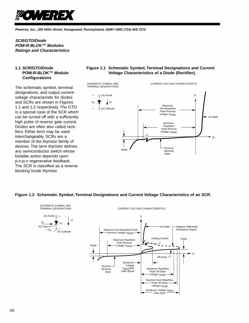
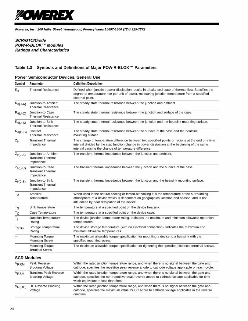
The schematic symbol, terminal designations, and output current-voltage characteristic for diodesand SCRs are shown in Figures1.1 and 1.2 respectively. The GTOis a special case of the SCR whichcan be turned off with a sufficientlyhigh pulse of reverse gate current.Diodes are often also called recti-fiers. Either term may be used interchangeably. SCRs are a member of the thyristor family ofdevices. The term thyristor definesany semiconductor switch whosebistable action depends uponp-n-p-n regenerative feedback.The SCR is classified as a reverseblocking triode thyristor.
Powerex, Inc., 200 Hillis Street, Youngwood, Pennsylvania 15697-1800 (724) 925-7272
SCR/GTO/Diode POW-R-BLOK™ ModulesRatings and Characteristics
viii
Figure 1. 1 Schematic Symbol , Terminal Designations and CurrentVoltage Characteristics of a Diode (Rectifier).
CURRENT VOLTAGE CHARACTERISTICSCHEMATIC SYMBOL ANDTERMINAL DESIGNATIONS
VF
IRRM
IF
ReverseBlockingState
On-State
Maximum Non-RepetitivePeak ReverseVoltage VRSM
Maximum Repetitive
Peak ReverseVoltage VRRM
VF IF
(A) Anode
(K) Cathode
+
—
Figure 1. 2 Schematic Symbol , Terminal Designations and Curren t Voltage Characteristics of an SCR.
CURRENT VOLTAGE CHARACTERISTICSSCHEMATIC SYMBOL ANDTERMINAL DESIGNATIONS
IG
(G) GateVG
VT
IT
(A) Anode
(K) Cathode+ —
—
+
VT
IT
On-State
IDRMHolding Current
Breakover Voltage V(BO)Gate Open
Breakover Voltage
V(BO)WithGate Signal
Maximum Non-Repetitive Peak Off-State Voltage VDSM
Maximum RepetitivePeak Off-State Voltage VDRM
Maximum Non-Repetitive PeakReverse Voltage VRSM
Maximum RepetitivePeak Reverse
Voltage VRRM
ReverseBlocking
State
Off-State
IRRM
Negitive DifferentialResistance Region

1.2 Typical Applications
Some of the typical applicationsfor POW-R-BLOK™ modules are:UPS, inverters, lighting controls,induction heating, ultrasonic cleaning, battery chargers, AC andDC motor control, high frequencywelding, and power supplies. Tomeet such a diverse range ofapplications, POW-R-BLOK™modules are available ina wide range of circuit configurations, as illustrated byTable 1.1.
Powerex, Inc., 200 Hillis Street, Youngwood, Pennsylvania 15697-1800 (724) 925-7272
SCR/GTO/Diode POW-R-BLOK™ ModulesRatings and Characteristics
ix
Table 1.1 POW-R-BLOK™ Module Circuit Configurations.DIODE MODULES
Single CS Series
Dual CD_1 SeriesED_1 Series
CommonCathode
CC SeriesEC Series
CommonAnode
CN SeriesEN Series
ReverseDual
CD_9 Series
ThreePhaseBridge
ME Series
SCR/DIODE (HALF CONTROL) MODULES
SCR/Diode CM_2 SeriesCD_2 SeriesED_2 SeriesCD_B Series
Diode/SCR CD_7 SeriesED_7 SeriesCD_C Series
Diode/SCRCenter Tap
CC_2 SeriesEC_2 Series
SCR/DiodeCenter Tap
CN_7 SeriesEN_7 Series
SplitSCR/Diode
CT_2 Series
SCR/DiodeThree-PhaseBridge
CE_2 SeriesDUAL SCR (FULL CONTROL) MODULES
Dual SCR CM_3 SeriesCD_3 SeriesED_3 SeriesCD_A Series
SplitDual SCR
CT_3 Series GTO BRIK
*Auxiliary Cathode Terminal Not Available On All Module Types
*Auxiliary Cathode Terminal Not Available On All Module Types
*
*

1.3 The Device Data Sheet
The proper application of power semiconductors requires an understanding of their maximumratings and electrical characteristics, information whichis presented within the device data sheet. Good design practiceemploys data sheet limits and notinformation obtained from smallsample lots.
A rating is a maximum or minimumvalue that sets a limit on devicecapability. Operation in excess of a rating can result in irreversibledegration or device failure.Maximum ratings representextreme capabilities of a device.They are not to be used as designconditions.
A characteristic is a measure ofdevice performance under specified operating conditionsexpressed by minimum, typical,and/or maximum values, or showngraphically.
Powerex, Inc., 200 Hillis Street, Youngwood, Pennsylvania 15697-1800 (724) 925-7272
SCR/GTO/Diode POW-R-BLOK™ ModulesRatings and Characteristics
x
Absolute Maxi mum Ratings
Characteristics Symbol CM421290 CM421690 Units
Peak Forward Blocking Voltage VDRM 1200 1600 Volts
Transient Peak Forward Blocking Voltage (Non-Repetitive), t < 5ms VDSM 1350 1700 Volts
DC Forward Blocking Voltage VD(DC) 960 1280 Volts
Peak Reverse Blocking Voltage VRRM 1200 1600 Volts
Transient Peak Reverse Blocking Voltage (Non-Repetitive), t < 5ms VRSM 1350 1700 Volts
DC Reverse Blocking Voltage VR(DC) 960 1280 Volts
RMS On-State Current IT(RMS), IF(RMS) 140 190 Amperes
Average On-State Current, TC = 82°C IT(AV), IF(AV) 90 90 Amperes
Peak One-Cycle Surge (Non-Repetitive) On-State Current (60Hz) ITSM, IF(TSM) 1800 1800 Amperes
Peak One-Cycle Surge (Non-Repetitive) On-State Current (50Hz) ITSM, IF(TSM) 1730 1730 Amperes
I2t (for Fusing), 8.3 milliseconds I2t 15000 15000 A2sec
Critical Rate-of-Rise of On-State Current* di/dt 100 100 Amperes/ms
Peak Gate Power Dissipation PGM 5.0 5.0 Watts
Average Gate Power Dissipation PG(AV) 0.5 0.5 Watts
Peak Forward Gate Voltage VGFM 10 10 Volts
Peak Reverse Gate Voltage VGRM 5.0 5.0 Volts
Peak Forward Gate Current IGFM 2.0 2.0 Amperes
Storage Temperature TSTG -40 to 125 -40 to 125 °C
Operating Temperature Tj -40 to 125 -40 to 125 °C
Maximum Mounting Torque M6 Mounting Screw — 26 26 lb.-in.
Maximum Mounting Torque M5 Terminal Screw — 17 17 lb.-in.
Module Weight (Typical) — 160 160 Grams
V Isolation VRMS 2500 2500 Volts
*Tj = 125°C, IG = 1.0A, VD = 1/2 VDRM
Table 1.2 Major Ratings and Characteristics of a Typical P OW-R-BLOK ™ Modul e.

Table 1.2 illustrates the major ratings and characteristics of atypical Powerex POW-R- BLOK™SCR/Diode Module. Table 1.3 liststhe symbols and definitions of themajor device parameters fordiodes, SCRs, and GTOs.
The remainder of this section onratings and characteristics will bespecific to SCRs. However, muchof the material is also applicable todiodes and GTOs.
Powerex, Inc., 200 Hillis Street, Youngwood, Pennsylvania 15697-1800 (724) 925-7272
SCR/GTO/Diode POW-R-BLOK™ ModulesRatings and Characteristics
xi
Electrical an d Thermal Characteristics , Tj = 25°C unless otherwise specified
Characteristics Symbol Test Conditions CM421290/CM421690 Units
Blo cking State Maxi mumsForward Leakage Current, Peak IDRM Tj = 125°C, VDRM = Rated 15 mA
Reverse Leakage Current, Peak IRRM Tj = 125°C, VRRM = Rated 15 mA
Conducting State Maxi mumsPeak On-State Voltage VFM IFM = 270A, ITM = 270A 1.4 Volts
Switching Mini mumsCritical Rate-of-Rise of Off-State Voltage dv/dt Tj = 125°C, VD = 2/3 VDRM 500 Volts/ms
Thermal Maxi mumsThermal Resistance, Junction-to-Case Ru(J-C) Per Module 0.3 °C/Watt
Thermal Resistance, Case-to-Sink (Lubricated) Ru(C-S) Per Module 0.2 °C/Watt
Gate Paramete rs Maxi mumsGate Current-to-Trigger IGT VD = 6V, RL = 2V 100 mA
Gate Voltage-to-Trigger VGT VD = 6V, RL = 2V 2.0 Volts
Non-Triggering Gate Voltage VGDM Tj = 125°C, VD = 1/2 VDRM 0.25 Volts
Table 1.2 Major Ratings and Characteristics of a Typical P OW-R-BLOK ™ Modul e. (Continued)
Powerex, Inc., 200 Hillis Street, Youngwood, Pennsylvania 15697-1800 (724) 925-7272
SCR/GTO/Diode POW-R-BLOK™ ModulesRatings and Characteristics
xii
Table 1.3 Symbols and Definitions of Major P OW-R-BLOK ™ Paramete rs
Power Semiconductor D evices , General Use
Symbol Parameter Definition/Description
Ru Thermal Resistance Defined when junction power dissipation results in a balanced state of thermal flow. Specifies the degree of temperature rise per unit of power, measuring junction temperature from a specified external point.
Ru(J-A) Junction-to-Ambient The steady state thermal resistance between the junction and ambient.Thermal Resistance
Ru(J-C) Junction-to-Case The steady state thermal resistance between the junction and surface of the case.Thermal Resistance
Ru(J-S) Junction-to-Sink The steady state thermal resistance between the junction and the heatsink mounting surface.Thermal Resistance
Ru(C-S) Contact The steady state thermal resistance between the surface of the case and the heatsinkThermal Resistance mounting surface.
Zu Transient Thermal The change of temperature difference between two specified points or regions at the end of a time Impedance interval divided by the step function change in power dissipation at the beginning of the same
interval causing the change of temperature difference.
Zu(J-A) Junction-to-Ambient The transient thermal impedance between the junction and ambient.Transient ThermalImpedance
Zu(J-C) Junction-to-Case The transient thermal impedance between the junction and the surface of the case.Transient ThermalImpedance
Zu(J-S) Junction-to-Sink The transient thermal impedance between the junction and the heatsink mounting surface.Transient ThermalImpedance
TA Ambient When used in the natural cooling or forced-air cooling it is the temperature of the surrounding Temperature atmosphere of a device which is dependent on geographical location and season, and is not
influenced by heat dissipation of the device.
TS Sink Temperature The temperature at a specified point on the device heatsink.
TC Case Temperature The temperature at a specified point on the device case.
Tj Junction Temperature The device junction temperature rating. Indicates the maximum and minimum allowable operation Rating temperatures.
TSTG Storage Temperature The device storage temperature (with no electrical connection). Indicates the maximum and Rating minimum allowable temperatures.
— Mounting Torque The maximum allowable torque specification for mounting a device to a heatsink with the Mounting Screw specified mounting screw.
— Mounting Torque The maximum allowable torque specification for tightening the specified electrical terminal screws.Terminal Screw
SCR ModulesVRRM Peak Reverse Within the rated junction temperature range, and when there is no signal between the gate and
Blocking Voltage cathode, specifies the repetitive peak reverse anode to cathode voltage applicable on each cycle.
VRSM Transient Peak Reverse Within the rated junction temperature range, and when there is no signal between the gate and Blocking Voltage cathode, specifies the non-repetitive peak reverse anode to cathode voltage applicable for time
width equivalent to less than 5ms.
VR(DC) DC Reverse Blocking Within the rated junction temperature range, and when there is no signal between the gate andVoltage cathode, specifies the maximum value for DC anore to cathode voltage applicable in the reverse
direction.

Powerex, Inc., 200 Hillis Street, Youngwood, Pennsylvania 15697-1800 (724) 925-7272
SCR/GTO/Diode POW-R-BLOK™ ModulesRatings and Characteristics
xiii
Table 1.3 Symbols and Definitions of Major P OW-R-BLOK ™ Paramete rs (continued)
SCR Modules (conti nued)
Symbol Parameter Definition/Description
VDRM Peak Forward Within the rated junction temperature range, and when there is no signal between the gate and Blocking Voltage cathode, specifies the repetitive peak off-state anode to cathode voltage applicable for each cycle.
Includes the maximum instantaneous value for repetitive off-state voltage, but excludes non-repetitive transient off-state voltage.
VDSM Transient Peak Forward Within the rated junction temperature range and when there is no signal between the gate and Blocking Voltage cathode, specifies the peak non-repetitive off-state anode to cathode voltage applicable for a time
width equivalent to less than 5ms. Indicates the maximum instantaneous value for non-repetitive transient off-state voltage.
VD(DC) DC Forward Within the rated junction temperature range and when there is no signal between the gate and Blocking Voltage cathode, specifies maximum value for DC anode to cathode voltage applicable in the
forward direction.
dv/dt Critical Rate-of-Rise At maximum rated junction temperature, and when there is no signal between the gate and cathode, of Off-State Voltage specifies the maximum rate-of-rise of off-state voltage that will not drive the device from an off-state
when an exponential off-state voltage of specified amplitude is applied to the device.
dv = 0.632VD VD: Specified Off-State Voltagedt r r: Time constant for exponential waveform
VTM Peak On-State At specified junction temperature, and when on-state current (commercial frequency, half sine wave Voltage of specified peak amplitude) is applied to the device, indicates peak-value for the resulting
voltage drop.
IT(RMS) RMS On-State At specified case temperature, indicates the RMS value for on-state current that can be continuouslyCurrent applied to the device.
IT(AV) Average On-State At specified case temperature, and with the device connected to a resistive or inductive load, Current indicates the average value for forward-current (sine half wave, commercial frequency) that can be
continuously applied to the device.
ITSM Peak On-State Within the rated junction temperature range, indicates the peak-value for non-repetitive on-state Current current (sine half wave, commercial frequency). This value indicated for one cycle, or as a function
of a number of cycles.
I2t Current-Squared Time The maximum, on-state, non-repetitive short time-thermal capacity of the device and is helpful in selecting a fuse or providing a coordinated protection scheme of the device in the equipment. This rating is intended specifically for operation less than one half cycle of a 180° (degree) conduction angle sinusoidal wave form. NOTE: The off-state blocking capability cannot be guaranteed at values near the maximum I2t.
di/dt Critical Rate-of-Rise At specified case (or point) temperature, specified off-state voltage, specified gate conditions, and at of On-State Current a frequency of less than 60Hz, indicates the maximum rate-of-rise of on-state current which the
thyristor will withstand after switching from an off-state to an on-state, when using recommended gate drive.
IRRM Reverse Leakage At maximum rated junction temperature, indicates the peak-value for reverse-current flow when a Current, Peak voltage (sine half wave, commercial frequency, and having a peak value as specified for repetitive
peak reverse-voltage rating) is applied in a reverse direction to the device.
IDRM Forward Leakage At maximum rated junction temperature, indicates the peak-value for off-state-current flow when a Current, Peak voltage (sine half wave, commercial frequency, and having a peak value for repetitive off-state
voltage rating) is applied in a forward direction to the device.
PGM Peak Gate Power Within the rated junction temperature range, indicates the peak-value for maximum allowable power Dissipation dissipation over a specified time period, when the device is in forward conduction between the
gate and cathode.
PG(AV) Average Gate Power Within the rated junction temperature range, indicates the average value for maximum allowable Dissipation power dissipation when the device is forward-conducting between the gate and cathode.

Powerex, Inc., 200 Hillis Street, Youngwood, Pennsylvania 15697-1800 (724) 925-7272
SCR/GTO/Diode POW-R-BLOK™ ModulesRatings and Characteristics
xiv
Table 1.3 Symbols and Definitions of Major P OW-R-BLOK ™ Paramete rs (continued)
SCR Modules (conti nued)
Symbol Parameter Definition/Description
IGFM Peak Forward Gate Within the rated junction temperature range, indicates the peak-value for forward-current flowCurrent between the gate and cathode.
VGRM Peak Reverse Gate Within the rated junction temperature range, indicates the peak-value for reverse-voltageVoltage applied between the gate and cathode.
VGFM Peak Forward Gate Within the rated junction temperature range, indicates the peak-value for forward-voltageVoltage applied between the gate and cathode.
IGT Gate Current- At a junction temperature of 25°C, and with a specified off-voltage, and a specified load resistance, to-Trigger indicates the minimum gate DC current required to switch the thyristor from an off-state to an
on-state.
VGT Gate Voltage- At a junction temperature of 25°C, and with a specified off-state voltage, and a specified load to-Trigger resistance, indicates the minimum gate DC voltage required to switch the thyristor from an off-state
to an on-state.
VGDM Non-Triggering Gate At maximum rated junction temperature, and with a specified off-state voltage applied to the Voltage device, indicates the maximum gate DC voltage which will not switch the device from an off-state
to an on-state.
ton Turn-On Time At specified junction temperature, and with a peak repetitive off-state voltage of half rated value, followed by device turn-on using specified gate-current, when specified on-state current of specified di/dt flows, indicated as the time required for the applied off-state voltage to drop to 10% of its initial value after gate current application. “Delay time” is the term used to define the time required for applied voltage to drop to 90% of its initial value following gate-current application, and the time required for level to drop from 90% to 10% is referred to as “rise time”. The sum of both these defines turn-on time.
tq Turn-Off Time Specified at maximum rated junction temperature. Device set up to conduct on-state current, followed by application of specified reverse-voltage to quench on-state current, and then increasing voltage at a specified rate-of-rise as determined by circuit conditions controlling the point where specified off-state voltage is reached. Turn-off time defines the minimum time which the device will hold its off-state, starting from the point on-state current reached zero, and after forward voltage is again applied.
Diod e Modules
VRRM Peak Reverse Within the rated junction temperature range, specifies the repetitive peak reverse voltage applicable Blocking Voltage for each cycle. Includes the maximum instantaneous value for repetitive transient reverse voltage,
but excludes non-repetitive transient reverse-voltage.
VRSM Transient Peak Reverse Within the rated junction temperature range, specifies the non-repetitive peak reverse voltage Blocking Voltage applicable for a time width equivalent to less than 5ms. Indicates the maximum instantaneous value
for non-repetitive transient voltage.
VR(DC) DC Reverse The maximum value for DC voltage applicable in the reverse direction, specified within the rated Blocking Voltage junction temperature range.
VFM Peak On-State At specified junction temperature, and when forward-current (commercial frequency, sine wave of Voltage specified peak amplitude) is applied to the device, indicates peak-value for the resulting
voltage drop.
IF(RMS) RMS On-State At specified case temperature, indicates the RMS value for forward-current that can be continuously Current applied to the device.
IF(AV) Average On-State At specified case temperature, and with the device connected to a resistive or inductive load, Current indicates the average value for forward-current (sine half wave, commercial frequency) that can be
continuously applied to the device.
IFSM Peak Surge On-State Within the rated junction temperature range, indicates the peak-value for non-repetitive Current forward-current (sine half wave, commercial frequency), this value is defined at one cycle or as a
function of a number of cycles.
tqCurrentVoltage
Time

Powerex, Inc., 200 Hillis Street, Youngwood, Pennsylvania 15697-1800 (724) 925-7272
SCR/GTO/Diode POW-R-BLOK™ ModulesRatings and Characteristics
xv
Table 1.3 Symbols and Definitions of Major P OW-R-BLOK ™ Paramete rs (continued)
Diod e Modules (continued)
Symbol Parameter Definition/Description
I2t Current-Squared Time The maximum, on-state, non-repetitive short time-thermal capacity of the device and is helpful in selecting a fuse or providing a coordinated protection scheme of the device in the equipment. This rating is intended specifically for operation less than one half cycle of a 180° (degree) conduction angle sinusoidal wave form. NOTE: The off-state blocking capability cannot be guaranteed at values near the maximum I2t.
IRRM Reverse Leakage At maximum rated junction temperature, indicates the peak-value for reverse-current flow when a Current, Peak voltage (sine half wave, commercial frequency, and having a peak value as specified for repetitive
peak reverse-voltage rating) is applied in a reverse direction to the device.
Qrr Reverse Recovery Indicates the total amount of reverse recovery charge. Specified at a certain junction temperature, Charge and current which has decreased at a specified rate of decrease, from the forward state to reverse
after a certain forward current was applied.
GTO Modules
VRRM Peak Reverse Within the rated junction temperature range, and when there is no signal between the gate and Blocking Voltage cathode, specifies the peak repetitive reverse-voltage applicable on each cycle.
VRSM Transient Peak Reverse Within the rated junction temperature range, and when there is no signal between the gate and Blocking Voltage cathode, specifies the peak non-repetitive peak reverse voltage applicable for a time width
equivalent to less than 5ms.
VDRM Peak Forward Within the rated junction temperature range, and when there is a specified reverse voltage between Blocking Voltage the gate and cathode, specifies the peak repetitive off-state voltage applicable for each cycle.
Includes the maximum instantaneous value for repetitive transient off-state voltage, but excludes non-repetitive off-state voltage.
VDSM Transient Peak Forward Within the rated junction temperature range, and when there is a specified reverse voltage between Blocking Voltage the gate and cathode, specifies the peak non-repetitive off-state voltage applicable for a time width
equivalent to less than 5ms. Indicates the maximum instantaneous value for non-repetitive transient off-state voltage.
VD(DC) DC Forward Within the rated junction temperature range, and when there is a specified reverse voltage between Blocking Voltage the gate and cathode, specifies maximum value for DC voltage applicable in the forward direction.
dv/dt Critical Rate-of-Rise At maximum rated junction temperature, and when there is a specified reverse voltage between the of Off-State Voltage gate and cathode, specifies the maximum rate-of-rise of off-state voltage that will not drive the
device from an off-state to an on-state when an exponential off-state voltage of specified amplitude is applied to the device.
dv = 0.632VD VD: Specified Off-State Voltagedt r r: Time constant for exponential waveform
VTM Peak On-State At specified junction temperature, and when on-state current (commercial frequency, half sine wave Voltage of specified peak amplitude) is applied to the device, indicates peak-value for the resulting voltage
drop.
IT(RMS) RMS On-State At specified case temperature, indicates the RMS value for on-state current that can be continuouslyCurrent applied to the device.
IT(AV) Average On-State At specified case temperature, and with the device connected to a resistive or inductive load, Current indicates the average value for forward-current (sine half wave, commercial frequency) that can be
continuously applied to the device.
ITSM Peak Surge On-State Within the rated junction temperature range, indicates the peak-value for non-repetitive on-state Current current (sine half wave, commercial frequency). This value indicated for one cycle, or as a function
of a number of cycles.

Powerex, Inc., 200 Hillis Street, Youngwood, Pennsylvania 15697-1800 (724) 925-7272
SCR/GTO/Diode POW-R-BLOK™ ModulesRatings and Characteristics
xvi
Table 1.3 Symbols and Definitions of Major P OW-R-BLOK ™ Paramete rs (continued)
GTO Modules (conti nued)
Symbol Parameter Definition/Description
I2t Current-Squared Time The maximum, on-state, non-repetitive short time-thermal capacity of the device and is helpful in selecting a fuse or providing a coordinated protection scheme of the device in the equipment. This rating is intended specifically for operation less than one half cycle of a 180° (degree) conduction angle sinusoidal wave form. NOTE: The off-state blocking capability cannot be guaranteed at values near the maximum I2t.
di/dt Critical Rate-of-Rise At specified case (or point) temperature, specified off-state voltage, specified gate conditions, and at of On-State Current a frequency of less than 60Hz, indicates the maximum rate-of-rise of on-state current which the
GTO will withstand after switching from an off-state to an on-state, when using recommended gate drive.
IRRM Reverse Leakage At maximum rated junction temperature, indicates the peak-value for reverse-current flow when a Current, Peak voltage (a half sine wave, commercial frequency, and having a peak value as specified for repetitive
peak reverse-voltage rating) is applied in a reverse direction to the device.
IDRM Forward Leakage At maximum rated junction temperature, indicates the peak-value for off-state-current flow when a Current, Peak voltage (sine half wave, commercial frequency, and having a peak value as specified for repetitive
off-state voltage rating) is applied in a forward direction to the device. Tested with a specified reversevoltage between the gate and cathode.
PGFM Peak Gate Forward Within the rated junction temperature range, indicates the peak-value for maximum allowable power Power Dissipation dissipation over a specified time period, when the device is forward conducting between the
gate and cathode.
PG(AV) Average Gate Forward Within the rated junction temperature range, indicates the average value for maximum allowable Power Dissipation power dissipation when the device is forward-conducting between the gate and cathode.
IGFM Peak Forward Gate Within the rated junction temperature range, indicates the peak-value for forward-current flowCurrent between the gate and cathode.
VGRM Peak Reverse Gate Within the rated junction temperature range, indicates the peak-value for reverse-voltageVoltage applied between the gate and cathode.
VGFM Peak Forward Gate Within the rated junction temperature range, indicates the peak-value for forward-voltageVoltage applied between the gate and cathode.
IGT Gate Current- At a junction temperature of 25°C, and with a specified off-voltage, and a specified load resistance, to-Trigger indicates the minimum gate DC current required to switch the GTO from an off-state to an
on-state.
VGT Gate Voltage- At a junction temperature of 25°C, and with a specified off-state voltage, and a specified load to-Trigger resistance, indicates the minimum gate DC voltage required to switch the GTO from an off-state
to an on-state.
PGRM Peak Gate Reverse Within the rated junction temperature range, indicates the peak-value for maximum allowable power Power Dissipation dissipation in the reverse direction between the gate and cathode, over a specified time period.
PGR(AV) Average Gate Reverse Within the rated junction temperature range, indicates the average value for maximum allowable Power Dissipation power dissipation in the reverse direction between the gate and cathode.
IGRM Peak Reverse Within the rated junction temperature range, indicates peak-value for reverse-current that can be Gate Current conducted between the gate and cathode.
ITGQ Gate Controlled Under specified conditions, indicates the instantaneous value for on-current usable in gate control, Turn-off Current specified immediately prior to device turn-off.
tgt Turn-On Time When applying forward-current to the gate, indicates the time required to switch the GTO from an off-state to an on-state.
tgq Turn-Off Time When applying reverse-current to the gate, indicates the time required to switch the GTO from an on-state to an off-state.

1.4 Voltage Ratings
The specified voltages are definedby the maximum rating voltageswhich can be applied betweenanode and cathode in the forward,(anode positive with respect to the cathode), and the reversedirections. The maximum voltageratings should never be exceeded.Exceeding the maximum voltageratings can be detrimental to thedevice, resulting in instant failureor a decrease in the life of thedevice.
The repetitive peak sinusoidal forward voltage which can beapplied to an SCR or a GTO in theoff-state is specified by the PeakForward Blocking Voltage, VDRM.The forward voltage applicable for sine pulses of less than 5 milliseconds duration which canbe applied on a non-repetitivebasis to an SCR or a GTO in theoff-state is specified by theTransient Peak Forward BlockingVoltage, VDSM. The maximum forward DC voltage rating for anSCR or a GTO is specified by theDC Forward Blocking Voltage,VD(DC). Similar parameters existwith respect to the reverse direction, i.e. Peak ReverseBlocking Voltage, VRRM; TransientPeak Reverse Blocking Voltage,VRSM; and DC Reverse BlockingVoltage, VR(DC). The reverseparameters are applicable todiodes in addition to SCRs andGTOs.
Voltage ratings are specified at the maximum rated junction temperature and are applicableover the entire operating temperature range. For mostSCRs, voltage ratings are
specified with the gate terminalopen. Of particular caution, usersshould avoid applying positivegate voltage during periods whenan SCR is blocking reverse voltage. Positive gate bias duringreverse anode to cathode voltageresults in a significant increase inSCR power dissipation which mustbe accounted for to insure reliableoperation. For GTOs, voltage ratings are specified with a stipulated value of reverse gate tocathode voltage. SCRs are normally assigned the same voltage rating in both the forwardand reverse directions. In practice,most SCRs exhibit a slightly higher reverse breakdown voltage,and the forward breakdown voltage sets the device rating.
Leakage currents are specified atthe device forward and reversevoltage ratings. Leakage currentsare strongly temperature dependent. At high junction temperatures, it is possible to haveregenerative thermal runaway ofthe device if the case to ambientthermal resistance is at or above acritical value. This potential highpower dissipation, particularly withpoor or no heatsinking is one reason why it is not recommendedto measure blocking voltages ofdiodes, SCRs, or GTOs with DCtests.
Exceeding the forward blockingvoltage of an SCR will result in triggering the device into conduction. Voltage breakover isgenerally not damaging providingthe allowable di/dt rating under thiscondition is not exceeded. Thebreakover voltage of an SCR ishighly temperature dependent,decreasing rapidly above rated
junction temperature. It is not recommended to trigger SCRs byvoltage breakover, rather a zenerdiode or equivalent network shouldbe connected from anode to gateso that the device is triggered by gate drive.
1.5 dv/dt Rating
A high rate of off-state anode-to-cathode voltage, dv/dt, may cause an SCR to turn-on. The static dv/dt test circuit and standard waveforms are shownin Figure 1.3.
Static dv/dt capability is an inversefunction of junction temperature.Reverse biasing the gate withrespect to the cathode mayincrease dv/dt withstand capabilityfor medium and low current SCRs.Often the circuit designer will needto add a snubber network acrossthe SCR to limit the maximumdv/dt applied to an SCR.
Powerex, Inc., 200 Hillis Street, Youngwood, Pennsylvania 15697-1800 (724) 925-7272
SCR/GTO/Diode POW-R-BLOK™ ModulesRatings and Characteristics
xvii
VO
63%
10%
Numerical dv/dt
Time
R1C1
to
(EXP) = 0.63dvdt
Vo
R1C1
4 R1C1
To Scope
GateBias
D. U. T.C1R3VAA
+
—
S1R1 R2
S1 = Mercury Wetted Reed Relay or SCRR1 = Noninducive ResistorR2 = Current Limiting Resistor
Figure 1. 3 Exponential dv/dtTest Ci rcuit andWaveform
1.6 Power Dissipation
The power generated in an SCRconsists of the following components:
1. Turn-on switching2. Conduction3. Turn-off switching or
commutation4. Blocking5. Gate Circuit
On-state conduction losses arethe major source of junction heating for normal duty cycles andpower frequencies. For very highdi/dt current waveforms or highoperating frequencies, turn-onswitching loss can become significant.
Figure 1.4 illustrates a typicalcurve of on-state power dissipationin average watts for an SCR as afunction of average current inamperes for various conductionangles for operation up to 400 Hz.These curves are based on a
current waveform which is theremainder of a half sine wavewhich results from delayed angletriggering in a single phase resistive load circuit. Similarcurves are provided forrectangular current waveforms.
These curves represent the integrated product of the instantaneous anode current andon-state voltage drop, and theintegration of the appropriatereverse blocking losses. Pulse triggering is assumed and hencegate losses are neglected.
1.7 Average and RMS CurrentRatings
Average current rating versus casetemperature as it appears in a typical curve for an SCR is shownin Figure 1.5. These curves specifythe maximum allowable averageanode current ratings of the SCRas a function of case temperatureand conduction angle for a resistive load operating up to 400 Hz. Points on this curve areselected so that the junction temperature does not exceed the
maximum allowable value. Thesecurves have definite end points forthe various conduction angles.These end points represent theRMS rating of the device. TheRMS current rating is necessary toprevent excessive heating of theresistive elements of the SCR,such as joints, leads, interfaces,etc. The relationship between theRMS value and the average valueof a current waveform is depen-dent upon the wave shape. For thedata sheet rating standard halfwave sinusoidal waveform, theratio of RMS to average values is1.57. For low duty cycle wave-forms, the average value can bewell within device ratings but thehigh peak currents can result inthe allowable RMS rating beingexceeded. Similar curves are provided for rectangular currentwaveforms, typical highly inductiveloads.
1.8 POW-R-BLOK ™ RatingCurves
In addition to the standard sineand square wave information,there are also families of curvesfor assemblies of AC switches, single and three-phase bridges.This latter group takes the designer one step closer in selecting a heatsink to satisfy hissystems needs.
The set of curves shown in Figure 1.6 for the single phase ACswitch will be used to demonstratehow the curves were constructed.This set of curves is for one (1)CD43_ _60 module mounted on aheatsink. The left hand verticalaxis is for total average power, theright hand vertical is for maximumallowable case temperature, the
Powerex, Inc., 200 Hillis Street, Youngwood, Pennsylvania 15697-1800 (724) 925-7272
SCR/GTO/Diode POW-R-BLOK™ ModulesRatings and Characteristics
xviii
Figure 1. 4 On-State PowerDissipation vs.Average CurrentCharacteristic Curve
Figure 1. 5 Average Current vs.Case TemperatureCharacteristic Curve
MAXIMUM ON-STATE POWER DISSIPATION(SINUSOIDAL WAVEFORM)
AVERAGE ON-STATE CURRENT, IT(AV), (AMPERES)
MA
XIM
UM
PO
WE
R D
ISS
IPA
TIO
N, P
AV
(MA
X),
(WA
TT
S)
0 5 2510 15 200
40
360ou
RESISTIVE,INDUCTIVE LOAD PERSINGLEELEMENT
5
10
15
20
25
30
35
u = 30o
120o
180o
60o
90o
50
MAXIMUM ALLOWABLE CASE TEMPERATURE(RECTANGULAR WAVEFORM)
AVERAGE ON-STATE CURRENT, IT(AV), (AMPERES)
MA
XIM
UM
ALL
OW
AB
LE C
AS
E T
EM
PE
RA
TU
RE
, TC
, (o C
)
0 5 2510 15 20 30 35 40
60
70
80
90
100
110
120
130
360ou
RESISTIVE, INDUCTIVELOAD PER SINGLE
ELEMENT
u = 30o 60o 90o
120o
180o 270o DC

horizontal axis is split betweencurrent and ambient temperature.
The first step is to plot the lefthand half of the curve. This information is available from themore familiar average power versus average current curve. Inthis case, only the 180° sine datais plotted. First the average currentis changed to RMS by the 2.22factor. The 2.22 factor takes current rating from average SCRcurrent to RMS switch current for180° sine. Then the average powerfor the AC switch is plotted as afunction of RMS switch current.The formula
TC = Tj – PAVGRu(J-C)
is used to determine the maximumallowable case temperature whilemaintaining the junction tempera-ture rating of 125°C. Three or fourpower levels were selected to dothe calculations to determine casetemperature limits. For instance, at108A RMS, the power dissipationis 150 watts. Ru(J-C) is deter-mined again from average powerand case temperature curves botha function of current. The value for
the CD43_ _60 is 0.183°C/W,based on the complete moduleand 180° sine. This yields
TC = 125°C – 150W x 0.183°C/W
TC = 98°C
A horizontal line is drawn from the150 watt level and it intersects theright hand vertical axis at 98°C.This process is continued until the maximum allowable case temperature axis is sufficientlyfilled.
The next step is to label the righthand horizontal axis with ambienttemperatures up to 125°C whichcorresponds to the maximum permitted junction temperature.The formula
TA = TC – PTOT x Ru(C-A)
is used to generate case-to-ambi-ent thermal impedance lineswhere:
TA = Ambient temperature
TC = Maximum allowable case temperature from above
PTOT = Total power dissipation
NOTE: If 3 modules were used asin three-phase AC switch, PTOTwould be the total power of allthree modules.
and
Ru(C-A) = Thermal impedance case-to-ambient.
The procedure is to take an average power dissipation and itscorresponding maximum allowablecase temperature and arbitrarilyselect Ru(c-a) values to calculatemaximum ambients. For example
TA = 98°C – 150W x 0.1°C/W
TA = 83°C
The intersection of the 83°C ambient and 98°C case temperature becomes a point onthe 0.1°C/W Ru(C-A) line. The linemay be drawn through this pointand the 125°C ambient which is acommon point to all Ru(C-A) lines.Another Ru(C-A) is chosen andthe procedure is repeated. If
Powerex, Inc., 200 Hillis Street, Youngwood, Pennsylvania 15697-1800 (724) 925-7272
SCR/GTO/Diode POW-R-BLOK™ ModulesRatings and Characteristics
xix
0 40 80 120 160 0 15 35 55 75 95 115
0
50
100
150
200
250
300
79
88
98
107
116
MA
XIM
UM
TO
TA
L P
OW
ER
DIS
SIP
AT
ION
, PT
OT, (
WA
TT
S)
AC SWITCH
1 CD43_ _60
MA
XIM
UM
ALL
OW
AB
LE
CA
SE
TE
MP
ER
AT
UR
E, (
0 C)
IRMS, (AMPERES) AMBIENT TEMPERATURE, (oC)
0.20.15 0.1
0.050.3
0.4
0.6
1.00.8
5
IRMS RθCA = oC/W
Figure 1. 6 Maximum Total Power Dissipation and Maxi mum Ambien t Temperature Curve for AC Switch Application

negative ambients are found,choose other values of averagepower and case temperature andcontinue the process until suffi-cient Ru(c-a) lines are drawn.
1.9 Sample P roblem
Assume one is trying to select adevice to use on a 50hp direct current machine. A current of 90 amperes is required from athree-phase 480 volt AC line withthe motor running at base speed.This assumes a 90% efficiency.Figure 1.7 is very useful in determining what heatsink rating isrequired for a given ambient. Ahorizontal line can be drawn fromthe 90 amp point on the ID curve.This line intersects with the case-to-heatsink curves on theright hand side of the illustration.Assuming a 40°C ambient aninterpolation is needed betweenthe 0.2°C/W and 0.3°C/W Ru(C-A)lines. This results in an Ru(C-A) of0.266°C/W. With three (3) POW-R-BLOK's mounted on acommon heatsink, the followingformula may be used to determinethe actual heatsink rating required.
Ru(S-A) = Ru(C-A) – Ru(C-S)N
where
Ru(S-A) = Sink-to-ambient thermal impedance
Ru(C-A) = Case-to-ambient thermal impedance
Ru(C-S) = Case-to-sink thermal impedance for a module, i.e.0.1°C/W
and
N = The quantity of POW-R-BLOK’s on the common sink.
The sink-to-ambient thermalimpedance is
Ru(S-A) =
0.266°C/W – 0.1°C/W3
Ru(S-A) = 0.23°C/W
This value of thermal impedance,however, only guarantees the junction temperature will not
exceed 125°C. This is not normallythe approach taken by designers.A safety margin is normallyapplied to keep the junction to alower value and provide addedsystem reliability. A simple methodto use with the curves at hand isto add the desired safety marginonto the actual maximum ambient.If 20° margin on junction temperature is desired in a 40°Cambient, extend the existing hori-zontal line so that it intersects withthe vertical 60°C line. This intersection lies on another Ru(C-A) line which is 0.2°C/W.This translates into a 0.17°C/Wheatsink to ambient thermalimpedance. This heatsink wouldguarantee that even with worstcase device parameters, the peakjunction temperature will notexceed 105°C.
Similar problems may be solvedwith any of the other sets ofcurves for AC switch or singlephase bridge configurations.
1.10 Surge and I 2t Ratings
For non-recurrent current overloads, the rated junction
Powerex, Inc., 200 Hillis Street, Youngwood, Pennsylvania 15697-1800 (724) 925-7272
SCR/GTO/Diode POW-R-BLOK™ ModulesRatings and Characteristics
xx
0 40 80 120 160 0 15 35 55 75 95 115
0
160
320
480
640
800
960
76
86
96
106
115
MA
XIM
UM
TO
TA
L P
OW
ER
DIS
SIP
AT
ION
, PT
OT, (
WA
TT
S)
MA
XIM
UM
ALL
OW
AB
LE
CA
SE
TE
MP
ER
AT
UR
E, (
o C)
IRMS/IDC, (AMPERES) AMBIENT TEMPERATURE, (oC)
5
3∅-BRIDGE AND AC SWITCH
3 CD43_ _60
RθCA = oC/W
0.2
0.15
0.1
0.05
0.3
0.4
IRMS
ID
IDC
IRMS
0.6 0.8
Figure 1. 7 Maximum Total Power Dissipation and Maxi mum Ambien t Temperature Curve for Three-Phase Bridge Application.

temperature can be exceeded fora brief instant as indicated by thesurge and I2t ratings. Non-recurrent ratings apply only whenthey are not repeated before thepeak junction temperature hasreturned to its maximum ratedvalue or less. Non-recurrent ratings apply to situations thatoccur no more than a limited, typically 100, number of times overthe life of the device. In determining the surge current rating, the device is assumed tobe at its rated junction temperature prior to application of the overload. Many of thedevice parameters are not specified or guaranteed immediately following the surgecurrent. Surge current ratings areprovided for one, three, or ten halfcycles of sinusoidal current at 60 Hz. The I2t rating is derivedfrom the single cycle surge currentrating. The “I” in I2t rating is theRMS value of the surge current,while it is a peak value in thesurge current rating. The I2t ratingis useful in coordinating fuses toprotect the SCR or diode.
1.11 di/dt Ratings
When the rate of rise of anode
current (di/dt) is very rapid compared to the spreading velocity of the turn-on processacross the junctions, local “hotspot” heating will occur. These “hot spots” may lead to localizedexcessive temperatures that candestroy the device.
The di/dt test circuit and standardwaveform are shown in Figure 1.8.The di/dt rating guarantees thatthe device will block voltage butdoes not guarantee maintenanceof device dynamic characteristicssuch as turn-off time and dv/dtcapability.
The circuit designer must considerall current sources when assessing di/dt. In particular, thedischarge current from a snubbernetwork must be included in deter-mining the application di/dt.
1.12 Reverse RecoveryCharacteristics
During commutation from forwardconduction to the off-state, SCRsand diodes display a transientreverse current that far exceedsthe maximum rated blocking current. This reverse current iscalled reverse recovery current
and its time integral is the recovered charge, Qrr. Figure 1.9illustrates a typical reverse recovery waveform and includesthe definition of reverse recoverytime, trr.
Both Qrr and trr are strongly circuitdependent as well as devicedependent. The peak on-state forward current prior to commutation as well as the commutation di/dt are significantcircuit variables. Recoveredcharge has a positive temperaturecoefficient. Diodes are available inpower modules in standard, fast,and super fast recovery times.With the exception of the EDSeries, POW-R-BRIK™ andOPEN-BRIK™ modules, the SCRsused in POW-R-BLOK™ moduleshave standard recovery times typical of power line frequencyapplications.
1.13 Thermal Resistance
Temperature calculations are simplified by using thermal resistance concepts. The flow ofheat through a thermal path as aresult of power dissipation is analogous to the flow of currentthrough a conductive path as a
Powerex, Inc., 200 Hillis Street, Youngwood, Pennsylvania 15697-1800 (724) 925-7272
SCR/GTO/Diode POW-R-BLOK™ ModulesRatings and Characteristics
xxi
ITM
IT
ITM2
Time
WAVEFORM TEST CIRCUIT
t1
didt
=ITM2t1
ACSupply C
R L DUT
Trigger
Pulse
L ≈ 1.68t1VDM
ITMC ≈ 5.6
t1ITM
VDMR ≈ 0.54
VDM
ITM
Test Parameter Recommended Values
≥ Twice Device Current Rating≥ Iµs≥ 60PPS Maximum Rated Value Rated Value 20V/20Ω, tr = Iµs, tr = 3µs≥ 1000 Hours
ITM
t1Test REP RateTest TemperatureOff-State VoltageGate Trigger PulseTest Duration
Figure 1. 8 di/d t Test Ci rcuit an d Waveform

result of a voltage source. Hence,knowing the power being dissipated in a device, and theambient temperature, the resultingjunction temperature can be calcu-lated using the total thermal resis-tance and the following equation.
Tj = TA + PT* Ru(J-A)
where:
Ru(J-A) = Total thermal resistance junction-to-ambient (°C/W)
PT = Total power dissipation (W)
Tj, TA = Junction, ambient temperature
The total thermal resistance isgiven by:
Ru(J-A) = RuJ-C) + Ru(C-S) + Ru(S-A)
where:
Ru(J-C) = Junction-to-casethermal resistance specified on data sheet (°C/W)
Ru(C-S) =Lubricated case-to-sink thermal resistance specified on data sheet (°C/W)
Ru(S-A)= Sink-to-ambient thermal resistance (°C/W)
The thermal resistance (Ru(J-C))specified for a device is always amaximum value, with a safety margin included to allow for production variations from lot tolot. The interface case-to-sink thermal resistance (Ru(C-S)) canbe significant and the data sheetvalue specified is for a baseplateproperly lubricated with thermalcompound.
1.14 Transient ThermalImpedance
For short or low duty cycle powerpulses, using the steady statethermal resistance will give conservative junction temperatures. In addition, usingthe average value of power dissipation will underestimate thepeak junction temperature. Thesolution is use of the transientthermal impedance curves (Figure 1.10 illustrates a typicaltransient thermal impedancecurve). For a power device subjected to single or very lowduty cycle, short duration powerpulses, the maximum allowablepower dissipation during the transient period can be substantially greater than thesteady state dissipation capability.
Powerex, Inc., 200 Hillis Street, Youngwood, Pennsylvania 15697-1800 (724) 925-7272
SCR/GTO/Diode POW-R-BLOK™ ModulesRatings and Characteristics
xxii
Figure 1. 9 Reverse RecoveryWaveform andParameterDefinitions
T0 T1 T2 T3T4
IR
0
IF/IT
Timetrr
Qrr
( (IR4
diRdt
Figure 1.1 0 Transien t Thermal Impedance Characteristic Curve
TIME, t, (SECONDS)
TRANSIENT THERMAL IMPEDANCECHARACTERISTICS (JUNCTION-TO-CASE)
0
0.10
0.20
0.30
0.40
TR
AN
SIE
NT
TH
ER
MA
L IM
PE
DA
NC
E, Z
u(J-
C)(
t), (
o C/W
AT
T)
100 101
0.35
0.25
0.15
0.05
10-3 10-2 10-1 100