section 13. parallel master port (pmp) - microchip
TRANSCRIPT
Section 13. Parallel Master Port (PMP)
Parallel M
asterP
ort (P
MP
)
13
Parallel M
asterP
ort (P
MP
)
13
HIGHLIGHTS
This section of the manual contains the following major topics:
13.1 Introduction .................................................................................................................. 13-2
13.2 Module Registers ......................................................................................................... 13-313.3 Slave Port Modes....................................................................................................... 13-1113.4 Master Port Modes..................................................................................................... 13-16
13.5 Application Examples................................................................................................. 13-2513.6 Operation in Power Save Modes ............................................................................... 13-2813.7 AC Electrical Specifications ....................................................................................... 13-29
13.8 Register Maps............................................................................................................ 13-3213.9 Related Application Notes.......................................................................................... 13-3313.10 Revision History ......................................................................................................... 13-34
© 2006 Microchip Technology Inc. Advance Information DS39713A-page 13-1

PIC24F Family Reference Manual
13.1 INTRODUCTION
The Parallel Master Port (PMP) is a parallel 8-bit I/O module specifically designed tocommunicate with a wide variety of parallel devices, such as communications peripherals, LCDs,external memory devices, and microcontrollers. Because the interface to parallel peripheralsvaries significantly, the PMP module is highly configurable.
Key features of the PMP module include:
• 8 Data Lines• Up to 16 Programmable Address Lines• Up to 2 Chip Select Lines
• Programmable Strobe Options:- individual read and write strobes, or - read/write strobe with enable strobe
• Address Auto-Increment/Auto-Decrement• Programmable Address/Data Multiplexing• Programmable Polarity on Control Signals
• Legacy Parallel Slave Port (PSP) Support• Enhanced Parallel Slave Support:
- address support
- 4-byte deep auto-incrementing buffer• Programmable Wait States
Figure 13-1: PMP Module Pinout and Connections to External Devices
PMA0
PMA14
PMA15
PMBE
PMRD
PMWR
PMD<7:0>
PMENB
PMRD/PMWR
PMCS1
PMA1
PMA<13:2>
PMALL
PMALH
PMA<7:0>PMA<15:8>
PMCS2
EEPROM
Address Bus
Data Bus
Control Lines
PIC24F
LCDFIFO
Microcontroller
8-Bit Data (with or without multiplexed addressing)
Up to 16-Bit Address
Parallel Master Port
Buffer
DS39713A-page 13-2 Advance Information © 2006 Microchip Technology Inc.

Section 13. Parallel Master Port (PMP)P
arallel Master
Po
rt (PM
P)
13
13.2 MODULE REGISTERS
The PMP module uses these Special Function Registers:
• PMCON• PMMODE• PMADDR/PMDOUT1
• PMDOUT2• PMDIN1• PMDIN2
• PMAEN• PMSTAT
13.2.1 PMCON Register
The Parallel Master Port Control register (Register 13-1) contains the bits that control much ofthe module’s basic functionality. A key bit is PMPEN, which is used to reset the module as wellas enable or disable the module. When the module is disabled, all the associated I/O pins revertto their designated I/O function. In addition, any read or write operations, active or pending, arestopped and the BUSY bit is cleared. The data within the module registers is retained, includingPMSTAT. Thus, the module could be disabled after a reception, and the last received data andstatus would still be available for processing. When the module is enabled, all buffer control logicis reset along with PMSTAT.
All other bits in the PMCON register control address multiplexing, enable various port controlsignals and select control signal polarity. These are discussed in more detail in Section 13.4.1“Parallel Master Port Configuration Options”.
13.2.2 PMMODE Register
The Parallel Master Port Mode register (Register 13-2) contains bits that control the operationalmodes of the module. Master/Slave mode selection, as well as configuration options for bothmodes, are set by this register. It also contains the universal status flag, BUSY, used in Mastermodes to indicate that an operation by the module is in progress.
Details on the use of the PMMODE bits to configure PMP operation are provided in Section 13.3“Slave Port Modes” and Section 13.4 “Master Port Modes”.
13.2.3 PMADDR/PMDOUT1 Register
Depending on the selected mode, this single register can have one of two functions. In Mastermodes, the register functions as PMADDR, the Parallel Port Address register (Register 13-3). Itcontains the address to which outgoing data is to be written to, as well as the chip select controlbits for addressing parallel slave devices.
In Slave modes, the register functions as PMDOUT1, and acts as a buffer for outgoing data. Itsoperation is described in Section 13.3.2 “Buffered Parallel Slave Port Mode”.
13.2.4 PMDOUT2 Register
The Parallel Master Port Data Output 2 register is only used in Slave mode for buffered outputdata. It is used in the same manner as PMDOUT1.
13.2.5 PMDIN1 and PMDIN2 Registers
The Parallel Master Port Data Input 1 and Data Input 2 registers are used to buffer incoming data.PMDIN1 is used by the module in both Master and Slave modes. In Slave mode, this register isused to hold data that is asynchronously clocked in. Its operation is described in Section 13.3.2“Buffered Parallel Slave Port Mode”.
In Master mode, PMDIN1 is the holding register for both incoming and outgoing data. Itsoperation in Master mode is described in Section 13.4.2 “Read Operation” and Section 13.4.3“Write Operation”.
PMDIN2 is only used in Buffered Slave modes for incoming data. Its operation is similar to thatof PMDIN1 in Buffered Slave modes.
© 2006 Microchip Technology Inc. Advance Information DS39713A-page 13-3

PIC24F Family Reference Manual
13.2.6 PMAEN Register
The Parallel Master Port Address Enable register (Register 13-4) controls the operation ofaddress and chip select pins associated with this module. Setting these bits allocates thecorresponding microcontroller pins to the PMP module; clearing the bits allocates the pins to portI/O or other peripheral modules associated with the pins.
13.2.7 PMSTAT Register
The Parallel Master Port Status register (Register 13-5) contains status bits associated withbuffered operating modes when the port is functioning as a Slave port. This includes the overflow,underflow, and full flag bits. These flags are discussed in detail in Section 13.3.2 “BufferedParallel Slave Port Mode”.
13.2.8 Additional Registers
In addition to the PMP-specific registers, the PADCFG1 register also affects the configuration ofthe PMP module. The PMPTTL bit (PADCFG1<0>) allows the user to select between TTL andSchmitt Trigger (ST) digital input buffers for greater compatibility with external circuits. SettingPMPTTL selects TTL input buffers; the default configuration is ST buffers.
The PADCFG1 register is also described in Section 29. “Real-Time Clock and Calendar(RTCC)”.
DS39713A-page 13-4 Advance Information © 2006 Microchip Technology Inc.

Section 13. Parallel Master Port (PMP)P
arallel Master
Po
rt (PM
P)
13
Register 13-1: PMCON: Parallel Master Port Control Register
R/W-0 U-0 R/W-0 R/W-0 R/W-0 R/W-0 R/W-0 R/W-0
PMPEN — PSIDL ADRMUX1 ADRMUX0 PTBEEN PTWREN PTRDEN
bit 15 bit 8
R/W-0 R/W-0 R/W-0(1) R/W-0(1) R/W-0(1) R/W-0 R/W-0 R/W-0
CSF1 CSF0 ALP CS2P CS1P BEP WRSP RDSP
bit 7 bit 0
Legend:
R = Readable bit W = Writable bit U = Unimplemented bit, read as ‘0’
-n = Value at Reset ‘1’ = Bit is set ‘0’ = Bit is cleared x = Bit is unknown
bit 15 PMPEN: Parallel Master Port Enable bit
1 = PMP enabled0 = PMP disabled, no off-chip access performed
bit 14 Unimplemented: Read as ‘0’
bit 13 PSIDL: Stop in Idle Mode bit1 = Discontinue module operation when device enters Idle mode0 = Continue module operation in Idle mode
bit 12-11 ADRMUX1:ADRMUX0: Address/Data Multiplexing Selection bits
11 = Reserved10 = All 16 bits of address are multiplexed on PMD<7:0> pins01 = Lower 8 bits of address are multiplexed on PMD<7:0> pins, upper 8 bits are on PMA<15:8>00 = Address and data appear on separate pins
bit 10 PTBEEN: Byte Enable Port Enable bit (16-Bit Master mode)
1 = PMBE port enabled0 = PMBE port disabled
bit 9 PTWREN: Write Enable Strobe Port Enable bit1 = PMWR/PMENB port enabled0 = PMWR/PMENB port disabled
bit 8 PTRDEN: Read/Write Strobe Port Enable bit1 = PMRD/PMWR port enabled0 = PMRD/PMWR port disabled
bit 7-6 CSF1:CSF0: Chip Select Function bits
11 = Reserved10 = PMCS1 and PMCS2 function as chip select01 = PMCS2 functions as chip select, PMCS1 functions as address bit 1400 = PMCS1 and PMCS2 function as address bits 15 and 14
bit 5 ALP: Address Latch Polarity bit(1)
1 = Active-high (PMALL and PMALH)0 = Active-low (PMALL and PMALH)
bit 4 CS2P: Chip Select 1 Polarity bit(1)
1 = Active-high (PMCS2)0 = Active-low (PMCS2)
bit 3 CS1P: Chip Select 0 Polarity bit(1)
1 = Active-high (PMCS1/PMCS2)0 = Active-low (PMCS1/PMCS2)
Note 1: These bits have no effect when their corresponding pins are used as address lines.
© 2006 Microchip Technology Inc. Advance Information DS39713A-page 13-5

PIC24F Family Reference Manual
bit 2 BEP: Byte Enable Polarity bit
1 = Byte enable active-high (PMBE)0 = Byte enable active-low (PMBE)
bit 1 WRSP: Write Strobe Polarity bitFor Slave Modes and Master Mode 2 (PMMODE<9:8> = 00, 01, 10):1 = Read strobe active-high (PMWR)0 = Read strobe active-low (PMWR)For Master Mode 1 (PMMODE<9:8> = 11):1 = Enable strobe active-high (PMENB)0 = Enable strobe active-low (PMENB)
bit 0 RDSP: Read Strobe Polarity bitFor Slave Modes and Master Mode 2 (PMMODE<9:8> = 00, 01, 10):1 = Read strobe active-high (PMRD)0 = Read strobe active-low (PMRD)For Master Mode 1 (PMMODE<9:8> = 11):1 = Read/write strobe active-high (PMRD/PMWR)0 = Read/write strobe active-low (PMRD/PMWR)
Register 13-1: PMCON: Parallel Master Port Control Register (Continued)
Note 1: These bits have no effect when their corresponding pins are used as address lines.
DS39713A-page 13-6 Advance Information © 2006 Microchip Technology Inc.

Section 13. Parallel Master Port (PMP)P
arallel Master
Po
rt (PM
P)
13
Register 13-2: PMMODE: Parallel Master Port Mode Register
R-0 R/W-0 R/W-0 R/W-0 R/W-0 R/W-0 R/W-0 R/W-0
BUSY IRQM1 IRQM0 INCM1 INCM0 MODE16 MODE1 MODE0
bit 15 bit 8
R/W-0 R/W-0 R/W-0 R/W-0 R/W-0 R/W-0 R/W-0 R/W-0
WAITB1(1) WAITB0(1) WAITM3 WAITM2 WAITM1 WAITM0 WAITE1(1) WAITE0(1)
bit 7 bit 0
Legend:
R = Readable bit W = Writable bit U = Unimplemented bit, read as ‘0’
-n = Value at Reset ‘1’ = Bit is set ‘0’ = Bit is cleared x = Bit is unknown
bit 15 BUSY: Busy bit (Master mode only)
1 = Port is busy0 = Port is not busy
bit 14-13 IRQM1:IRQM0: Interrupt Request Mode bits 11 = Interrupt generated when Read Buffer 3 is read or Write Buffer 3 is written (Buffered PSP mode),
or on a read or write operation when PMA<1:0> = 11 (Addressable PSP mode only)10 = Reserved01 = Interrupt generated at the end of the read/write cycle00 = No Interrupt generated
bit 12-11 INCM1:INCM0: Increment Mode bits 11 = PSP read and write buffers auto-increment (Legacy PSP mode only)10 = Decrement ADDR<15,13:0> by 1 every read/write cycle01 = Increment ADDR<15,13:0> by 1 every read/write cycle00 = No increment or decrement of address
bit 10 MODE16: 8/16-Bit Mode bit 1 = 16-Bit mode: data register is 16 bits, a read or write to the data register invokes two 8-bit transfers0 = 8-Bit mode: data register is 8 bits, a read or write to the data register invokes one 8-bit transfer
bit 9-8 MODE1:MODE0: Parallel Port Mode Select bits
11 = Master Mode 1 (PMCSx, PMRD/PMWR, PMENB, PMBE, PMA<x:0> and PMD<7:0>)10 = Master Mode 2 (PMCSx, PMRD, PMWR, PMBE, PMA<x:0> and PMD<7:0>)01 = Enhanced PSP, control signals (PMRD, PMWR, PMCSx, PMD<7:0> and PMA<1:0>)00 = Legacy Parallel Slave Port, control signals (PMRD, PMWR, PMCSx and PMD<7:0>)
bit 7-6 WAITB1:WAITB0: Data Setup to Read/Write Wait State Configuration bits(1)
11 = Data wait of 4 TCY; multiplexed address phase of 4 TCY
10 = Data wait of 3 TCY; multiplexed address phase of 3 TCY
01 = Data wait of 2 TCY; multiplexed address phase of 2 TCY
00 = Data wait of 1 TCY; multiplexed address phase of 1 TCY
bit 5-2 WAITM3:WAITM0: Read to Byte Enable Strobe Wait State Configuration bits
1111 = Wait of additional 15 TCY
...0001 = Wait of additional 1 TCY
0000 = No additional Wait cycles (operation forced into one TCY)
bit 1-0 WAITE1:WAITE0: Data Hold After Strobe Wait State Configuration bits(1)
11 = Wait of 4 TCY
10 = Wait of 3 TCY
01 = Wait of 2 TCY
00 = Wait of 1 TCY
Note 1: WAITBx and WAITEx bits are ignored whenever WAITM3:WAITM0 = 0000.
© 2006 Microchip Technology Inc. Advance Information DS39713A-page 13-7

PIC24F Family Reference Manual
Register 13-3: PMADDR: Parallel Master Port Address Register (Master modes only)(1)
R/W-0 R/W-0 R/W-0 R/W-0 R/W-0 R/W-0 R/W-0 R/W-0
CS2 CS1 ADDR<13:8>
bit 15 bit 8
R/W-0 R/W-0 R/W-0 R/W-0 R/W-0 R/W-0 R/W-0 R/W-0
ADDR<7:0>
bit 7 bit 0
Legend:
R = Readable bit W = Writable bit U = Unimplemented bit, read as ‘0’
-n = Value at Reset ‘1’ = Bit is set ‘0’ = Bit is cleared x = Bit is unknown
bit 15 CS2: Chip Select 2 bit
If PMCON<7:6> = 10 or 01:1 = Chip Select 2 is active 0 = Chip Select 2 is inactiveIf PMCON<7:6> = 11 or 00:Bit functions as ADDR<15>.
bit 14 CS1: Chip Select 1 bit If PMCON<7:6> = 10:1 = Chip Select 1 is active0 = Chip Select 1 is inactive
If PMCON<7:6> = 11 or 0x:Bit functions as ADDR<14>.
bit 13-0 ADDR13:ADDR0: Destination Address bits
Note 1: In Enhanced Slave mode, PMADDR functions as PMDOUT1, one of the two data buffer registers. See Section 13.2.3 “PMADDR/PMDOUT1 Register” for information.
DS39713A-page 13-8 Advance Information © 2006 Microchip Technology Inc.

Section 13. Parallel Master Port (PMP)P
arallel Master
Po
rt (PM
P)
13
Register 13-4: PMAEN: Parallel Master Port Address Enable Register
R/W-0 R/W-0 R/W-0 R/W-0 R/W-0 R/W-0 R/W-0 R/W-0
PTEN15 PTEN14 PTEN13 PTEN12 PTEN11 PTEN10 PTEN9 PTEN8
bit 15 bit 8
R/W-0 R/W-0 R/W-0 R/W-0 R/W-0 R/W-0 R/W-0 R/W-0
PTEN7 PTEN6 PTEN5 PTEN4 PTEN3 PTEN2 PTEN1 PTEN0
bit 7 bit 0
Legend:
R = Readable bit W = Writable bit U = Unimplemented bit, read as ‘0’
-n = Value at Reset ‘1’ = Bit is set ‘0’ = Bit is cleared x = Bit is unknown
bit 15 PTEN15: PMCS2 Strobe Enable bit1 = PMA15 functions as either PMA<15> or PMCS20 = PMA15 functions as port I/O
bit 14 PTEN14: PMCS1 Strobe Enable bit1 = PMA14 functions as either PMA<14> or PMCS10 = PMA14 functions as port I/O
bit 13-2 PTEN13:PTEN2: PMP Address Port Enable bits
1 = PMA<13:2> function as PMP address lines0 = PMA<13:2> function as port I/O
bit 1-0 PTEN1:PTEN0: PMALH/PMALL Strobe Enable bits1 = PMA1 and PMA0 function as either PMA<1:0> or PMALH and PMALL0 = PMA1 and PMA0 function as port I/O
© 2006 Microchip Technology Inc. Advance Information DS39713A-page 13-9

PIC24F Family Reference Manual
Register 13-5: PMSTAT: Parallel Master Port Status Register (Slave mode only)
R-0 R/W-0 HS U-0 U-0 R-0 R-0 R-0 R-0
IBF IBOV — — IB3F IB2F IB1F IB0F
bit 15 bit 8
R-1 R/W-0 HS U-0 U-0 R-1 R-1 R-1 R-1
OBE OBUF — — OB3E OB2E OB1E OB0E
bit 7 bit 0
Legend: HS = Hardware Set HC = Hardware Cleared
R = Readable bit W = Writable bit U = Unimplemented bit, read as ‘0’
-n = Value at Reset ‘1’ = Bit is set ‘0’ = Bit is cleared x = Bit is unknown
bit 15 IBF: Input Buffer Full Status bit
1 = All writable input buffer registers are full0 = Some or all of the writable input buffer registers are empty
bit 14 IBOV: Input Buffer Overflow Status bit 1 = A write attempt to a full input byte register occurred (must be cleared in software)0 = No overflow occurred
bit 13-12 Unimplemented: Read as ‘0’
bit 11-8 IBnF: Input Buffer n Status Full bit
1 = Input buffer contains data that has not been read (reading buffer will clear this bit)0 = Input buffer does not contain any unread data
bit 7 OBE: Output Buffer Empty Status bit 1 = All readable output buffer registers are empty0 = Some or all of the readable output buffer registers are full
bit 6 OBUF: Output Buffer Underflow Status bit 1 = A read occurred from an empty output byte register (must be cleared in software)0 = No underflow occurred
bit 5-4 Unimplemented: Read as ‘0’
bit 3-0 OBnE: Output Buffer n Status Empty bit 1 = Output buffer is empty (writing data to the buffer will clear this bit)0 = Output buffer contains data that has not been transmitted
DS39713A-page 13-10 Advance Information © 2006 Microchip Technology Inc.

Section 13. Parallel Master Port (PMP)P
arallel Master
Po
rt (PM
P)
13
13.3 SLAVE PORT MODES
In Slave mode, the PMP module provides an 8-bit data bus and all the necessary control signalsto operate as a slave parallel device. It is also configurable for operation in Legacy, Buffered andAddressable modes. Slave mode provides several options for a more flexible interface:
• 8-bit data bus• 2 address lines (Addressable mode only)
• 3 control lines (read, write and chip select)• Selectable polarity on all control lines
To use the PMP as a slave, the module must be enabled (PMPEN = 1) and the mode must beset to one of the two possible Slave modes (PMMODE<9:8> = 01 or 00).
13.3.1 Legacy Mode
In Legacy mode (PMPEN = 1 and PMMODE<9:8> = 00), the module is configured as a parallelslave port with the associated enable module pins dedicated to the module. In this mode, anexternal device, such as another microcontroller or microprocessor, can asynchronously readand write data using the 8-bit data bus (PMD<7:0>), the read (PMRD), write (PMWR) and chipselect (PMCSx) inputs.
Figure 13-2: Parallel Master/Slave Connection Example
13.3.1.1 WRITE TO SLAVE PORT
When chip select is active and a write strobe occurs (PMCS1 = 1 and PMWR = 1), the datafrom PMD<7:0> is captured into the lower 8 bits of the PMDIN1 register (PMDIN1<7:0>). ThePMPIF and IBF flag bits are set when the write ends.
The timing for the control signals in Write mode is shown in Figure 13-3. The polarity of thecontrol signals is configurable.
Note: PMCS1 is used as the chip select input in all Slave modes. PMCS2 is only used inMaster modes.
PMD<7:0>
PMRD
PMWR
Master
Data Bus
Control Lines
PMCSx
PMD<7:0>
PMRD
PMWR
PIC24F Slave
PMCS1
Note 1: The relationship between the P clock and system clock cycles, shown inFigure 13-3 and Figure 13-4, apply to all timing diagrams shown in this section.
© 2006 Microchip Technology Inc. Advance Information DS39713A-page 13-11

PIC24F Family Reference Manual
Figure 13-3: Parallel Slave Port Write Waveforms
13.3.1.2 READ FROM SLAVE PORT
When chip select is active and a read strobe occurs (PMCS1 = 1 and PMRD = 1), the data fromthe lower 8 bits of the PMDOUT1 register (PMDOUT1<7:0>) is presented onto PMD<7:0>. Thedata in PMDIN1<7:0> is read out, and the Output Buffer Empty flag, OBE, is set. If the user writesnew data to PMDIN1<7:0> to clear OBE, the data is immediately read out; however, the OBE isnot cleared.
The timing for the control signals in Read mode is shown in Figure 13-4.
Figure 13-4: Parallel Slave Port Read Waveforms
13.3.1.3 INTERRUPT OPERATION
When either the PMCS1 or PMRD lines are detected high, the port pins return to the input stateand the PMPIF bit is set. User applications should wait for PMPIF to be set before servicing themodule. When this happens, the IBF and OBE bits can be polled and the appropriate action taken.
PMCS1
P4 P1 P2 P3 P4
PMWR
PMRD
IBF
OBE
PMPIF
PMD<7:0>
P1 P2
SystemClock
PMCS1
P4 P1 P2 P3 P4
PMWR
IBF
PMPIF
PMRD
OBE
PMD<7:0>
P1 P2
SystemClock
DS39713A-page 13-12 Advance Information © 2006 Microchip Technology Inc.
Section 13. Parallel Master Port (PMP)P
arallel Master
Po
rt (PM
P)
13
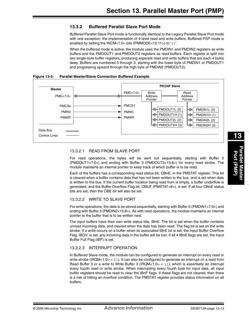
13.3.2 Buffered Parallel Slave Port Mode
Buffered Parallel Slave Port mode is functionally identical to the Legacy Parallel Slave Port modewith one exception: the implementation of 4-level read and write buffers. Buffered PSP mode isenabled by setting the INCM<1:0> bits (PMMODE<12:11>) to ‘11’.
When the buffered mode is active, the module uses the PMDIN1 and PMDIN2 registers as writebuffers and the PMDOUT1 and PMDOUT2 registers as read buffers. Each register is split intotwo single-byte buffer registers, producing separate read and write buffers that are each 4 bytesdeep. Buffers are numbered 0 through 3, starting with the lower byte of PMDIN1 or PMDOUT1and progressing upward through the high byte of PMDIN2 (PMDOUT2).
Figure 13-5: Parallel Master/Slave Connection Buffered Example
13.3.2.1 READ FROM SLAVE PORT
For read operations, the bytes will be sent out sequentially, starting with Buffer 0(PMDOUT1<7:0>) and ending with Buffer 3 (PMDOUT2<15:8>) for every read strobe. Themodule maintains an internal pointer to keep track of which buffer is to be read.
Each of the buffers has a corresponding read status bit, OBnE, in the PMSTAT register. This bitis cleared when a buffer contains data that has not been written to the bus, and is set when datais written to the bus. If the current buffer location being read from is empty, a buffer underflow isgenerated, and the Buffer Overflow Flag bit, OBUF (PMSTAT<6>), is set. If all four OBnE statusbits are set, then the OBE bit will also be set.
13.3.2.2 WRITE TO SLAVE PORT
For write operations, the data is be stored sequentially, starting with Buffer 0 (PMDIN1<7:0>) andending with Buffer 3 (PMDIN2<15:8>). As with read operations, the module maintains an internalpointer to the buffer that is to be written next.
The input buffers have their own write status bits, IBnE. The bit is set when the buffer containsunread incoming data, and cleared when the data has been read. The flag bit is set on the writestrobe. If a write occurs on a buffer when its associated IBnE bit is set, the Input Buffer OverflowFlag, IBOV, is set; any incoming data in the buffer will be lost. If all 4 IBnE flags are set, the InputBuffer Full Flag (IBF) is set.
13.3.2.3 INTERRUPT OPERATION
In Buffered Slave mode, the module can be configured to generate an interrupt on every read orwrite strobe (IRQM<1:0> = 01). It can also be configured to generate an interrupt on a read fromRead Buffer 3 or a write to Write Buffer 3 (IRQM<1:0> = 11), which is essentially an interruptevery fourth read or write strobe. When interrupting every fourth byte for input data, all inputbuffer registers should be read to clear the IBnF flags. If these flags are not cleared, then thereis a risk of hitting an overflow condition. The PMSTAT register provides status information on allbuffers.
PMD<7:0>
PMRD
PMWR
Master
Data Bus
Control Lines
PMCSx
PMRD
PMWR
PIC24F Slave
PMCS1PMDOUT1L (0)
PMDOUT1H (1)
PMDOUT2L (2)
PMDOUT2H (3)
PMDIN1L (0)
PMDIN1H (1)
PMDIN2L (2)
PMDIN2H (3)
PMD<7:0> WriteAddressPointer
ReadAddressPointer
© 2006 Microchip Technology Inc. Advance Information DS39713A-page 13-13

PIC24F Family Reference Manual
13.3.3 Addressable Parallel Slave Port Mode
In Addressable Parallel Slave Port mode, the module is configured with two extra inputs,PMA<1:0>. This makes the 4-byte buffer space directly addressable as fixed pairs of read andwrite buffers. The Addressable PSP mode is enabled by setting the MODE<1:0> bits(PMMODE<9:8>) to ‘01’. As with Buffered Legacy mode, data is output from PMDOUT1 andPMDOUT2 and is read in PMDIN1 and PMDIN2. Table 13-1 shows the address resolution for theincoming address to the input and output registers.
Table 13-1: Slave Mode Address Resolution
Figure 13-6: Parallel Master/Slave Connection Addressed Buffer Example
13.3.3.1 READ FROM SLAVE PORT
When chip select is active and a read strobe occurs (PMCS1 = 1 and PMRD = 1), the data fromone of the four output bytes is presented onto PMD<7:0>. Which byte is read depends on the2-bit address placed on PMA<1:0>. Table 13-1 shows the corresponding output registers andtheir associated address. When an output buffer is read, the corresponding OBnE bit is set. TheOBE flag bit is set when all the buffers are empty. If any buffer is already empty, OBnE = 1, thenext read to that buffer will set the OBUF (PMSTAT<6>) flag.
PMA<1:0> Output Register (Buffer) Input Register (Buffer)
00 PMDOUT1<7:0> (0) PMDIN1<7:0> (0)
01 PMDOUT1<15:8> (1) PMDIN1<15:8> (1)
10 PMDOUT2<7:0> (2) PMDIN2<7:0> (2)
11 PMDOUT2<15:8> (3) PMDIN2<15:8> (3)
PMD<7:0>
PMRD
PMWR
Master
PMCSx
PMA<1:0>
Address Bus
Data Bus
Control Lines
PMRD
PMWR
PIC24F Slave
PMCS1
PMDOUT1L (0)
PMDOUT1H (1)
PMDOUT2L (2)
PMDOUT2H (3)
PMDIN1L (0)
PMDIN1H (1)
PMDIN2L (2)
PMDIN2H (3)
PMD<7:0> WriteAddressDecode
ReadAddressDecode
PMA<1:0>
DS39713A-page 13-14 Advance Information © 2006 Microchip Technology Inc.

Section 13. Parallel Master Port (PMP)P
arallel Master
Po
rt (PM
P)
13
Figure 13-7: Parallel Slave Port Read Waveforms
13.3.3.2 WRITE TO SLAVE PORT
When chip select is active and a write strobe occurs (PMCS1 = 1 and PMWR = 1), the data fromPMD<7:0> is captured into one of the four input buffer bytes. Which byte is written depends onthe 2-bit address placed on PMA<1:0>. Table 13-1 shows the corresponding input registers andtheir associated address.
When an input buffer is written, the corresponding IBnF bit is set. The IBF flag bit is set when allthe buffers are written. If any buffer is already written, IBnF = 1, the next write strobe to that bufferwill generate an OBUF event and the byte will be discarded.
Figure 13-8: Parallel Slave Port Write Waveforms
13.3.3.3 INTERRUPT OPERATION
In Addressable PSP mode, the module can be configured to generate an interrupt on every reador write strobe. It can also be configured to generate an interrupt on any read from Read Buffer 3or write to Write Buffer 3; in other words, an interrupt will occur whenever a read or write occurswhen the PMA<1:0> pins are ‘11’.
PMCS1
P4 P1 P2 P3 P4
PMWR
PMA<1:0>
PSPIF
PMRD
OBE
PMD<7:0>
P1 P2
PMCS1
P4 P1 P2 P3 P4
PMWR
PMRD
IBF
PMPIF
PMD<7:0>
PMA<1:0>
P1 P2
© 2006 Microchip Technology Inc. Advance Information DS39713A-page 13-15

PIC24F Family Reference Manual
13.4 MASTER PORT MODES
In its Master modes, the PMP module provides an 8-bit data bus, up to 16 bits of address and allthe necessary control signals to operate a variety of external parallel devices, such as memorydevices, peripherals and slave microcontrollers. To use the PMP as a master, the module mustbe enabled (PMPEN = 1) and the mode must be set to one of the two possible Master modes(PMMODE<9:8> = 10 or 11).
Because there are a number of parallel devices with a variety of control methods, the PMPmodule is designed to be extremely flexible to accommodate a range of configurations. Some ofthese features include:
• 8 and 16-Bit Data modes on an 8-bit data bus• Configurable address/data multiplexing• Up to 2 chip select lines
• Up to 16 selectable address lines• Address auto-increment and auto-decrement• Selectable polarity on all control lines
• Configurable Wait states at different stages of the read/write cycle
13.4.1 Parallel Master Port Configuration Options
13.4.1.1 CHIP SELECTS
Up to two chip select lines, PMCS1 and PMCS2, are available for the Master modes of the PMP.The two chip select lines are multiplexed with the Most Significant bits of the address bus(PMA<14> and PMA<15>). When a pin is configured as a chip select, it is not included in anyaddress auto-increment/decrement. The function of the chip select signals is configured usingthe Chip Select Function bits, CSF<1:0> (PMCON <7:6>).
13.4.1.2 PORT PIN CONTROL
There are several bits available to configure the presence or absence of control and addresssignals in the module. These bits are PTRBEEN, PTWREN, PTRDEN and PTEN<15:0>. Theygive the user the ability to conserve pins for other functions and allow flexibility to control theexternal address. When any one of these bits is set, the associated function is present on itsassociated pin; when clear, the associated pin reverts to its defined I/O port function.
Setting a PTENx bit will enable the associated pin as an address pin and drive the correspondingdata contained in the PMADDR register. Clearing the PTENx bit will force the pin to revert to itsoriginal I/O function.
For the pins configured as chip select (PMCS1 or PMCS2) with the corresponding PTENx bit set,chip select pins drive inactive data (configured through the CSxP bits in PMCON) when a reador write operation is not being performed. The PTEN0 and PTEN1 bits also control the PMALLand PMALH signals. When multiplexing is used, the associated address latch signals should beenabled.
13.4.1.3 ADDRESS MULTIPLEXING
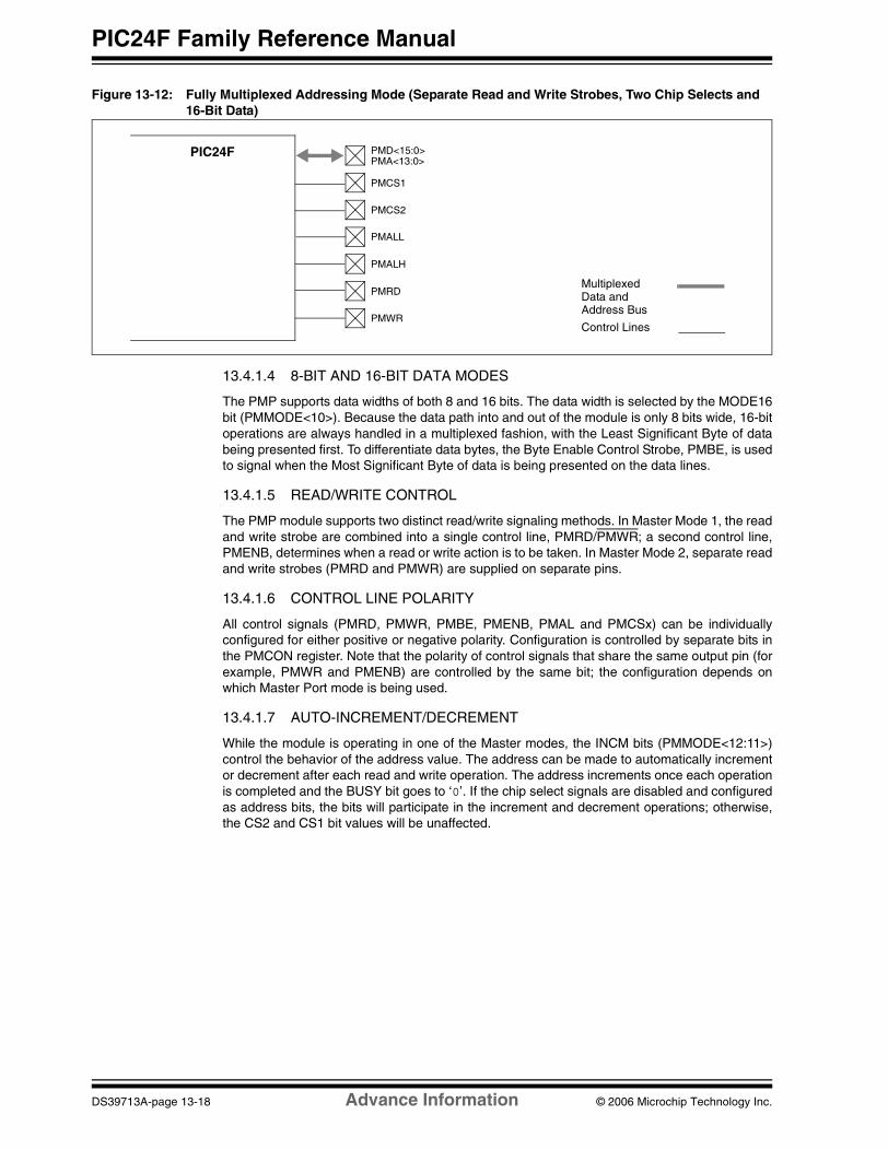
In either of the Master modes (MODE1:MODE0 = 1x), the user can configure the address busto be multiplexed together with the data bus. This is accomplished using theADRMUX1:ADRMUX0 bits. There are three Address Multiplexing modes available. Typicalpinout configurations for these modes are shown in Figure 13-9, Figure 13-10 and Figure 13-11.
In Demultiplexed mode (ADRMUX1:ADRMUX0 = 00), data and address information arecompletely separated. Data bits are presented on PMD<7:0> and address bits are presented onPMA<15:0>.
In Partially Multiplexed mode (ADRMUX1:ADRMUX0 = 01), the lower eight bits of the address aremultiplexed with the data pins on PMD<7:0>. The upper eight bits of the address are unaffectedand are presented on PMA<15:8>. The PMA<0> pin is used as an address latch, and presents theAddress Latch Low enable strobe (PMALL). The read and write sequences are extended by acomplete CPU cycle, during which, the address is presented on the PMD<7:0> pins.
DS39713A-page 13-16 Advance Information © 2006 Microchip Technology Inc.

Section 13. Parallel Master Port (PMP)P
arallel Master
Po
rt (PM
P)
13
In Fully Multiplexed mode (ADRMUX1:ADRMUX0 = 10), the entire 16 bits of the address aremultiplexed with the data pins on PMD<7:0>. The PMA<0> and PMA<1> pins are used topresent Address Latch Low enable (PMALL) and Address Latch High enable (PMALH) strobes,respectively. The read and write sequences are extended by two complete CPU cycles. Duringthe first cycle the lower eight bits of the address are presented on the PMD<7:0> pins with thePMALL strobe active. During the second cycle, the upper eight bits of the address are pre-sented on the PMD<7:0> pins with the PMALH strobe active. In the event the upper addressbits are configured as chip select pins, the corresponding address bits are automatically forcedto ‘0’.
For sample timings of the different multiplexing modes, see Section 13.4.5 “Master Mode Timing”.
Figure 13-9: Demultiplexed Addressing Mode (Separate Read and Write Strobes, Two Chip Selects)
Figure 13-10: Partially Multiplexed Addressing Mode (Separate Read and Write Strobes, Two Chip Selects)
Figure 13-11: Fully Multiplexed Addressing Mode (Separate Read and Write Strobes, Two Chip Selects)
PMRD
PMWR
PMD<7:0>
PMCS1
PMA<13:0>
PMCS2
PIC24F
Address Bus
Data Bus
Control Lines
PMRD
PMWR
PMD<7:0>
PMCS1
PMA<13:8>
PMALL
PMA<7:0>
PMCS2
PIC24F
Address Bus
MultiplexedData andAddress Bus
Control Lines
PMRD
PMWR
PMD<7:0>
PMCS1
PMALH
PMA<13:0>
PMCS2
PIC24F
MultiplexedData andAddress Bus
Control Lines
PMALL
© 2006 Microchip Technology Inc. Advance Information DS39713A-page 13-17
PIC24F Family Reference Manual
Figure 13-12: Fully Multiplexed Addressing Mode (Separate Read and Write Strobes, Two Chip Selects and 16-Bit Data)
13.4.1.4 8-BIT AND 16-BIT DATA MODES
The PMP supports data widths of both 8 and 16 bits. The data width is selected by the MODE16bit (PMMODE<10>). Because the data path into and out of the module is only 8 bits wide, 16-bitoperations are always handled in a multiplexed fashion, with the Least Significant Byte of databeing presented first. To differentiate data bytes, the Byte Enable Control Strobe, PMBE, is usedto signal when the Most Significant Byte of data is being presented on the data lines.
13.4.1.5 READ/WRITE CONTROL
The PMP module supports two distinct read/write signaling methods. In Master Mode 1, the readand write strobe are combined into a single control line, PMRD/PMWR; a second control line,PMENB, determines when a read or write action is to be taken. In Master Mode 2, separate readand write strobes (PMRD and PMWR) are supplied on separate pins.
13.4.1.6 CONTROL LINE POLARITY
All control signals (PMRD, PMWR, PMBE, PMENB, PMAL and PMCSx) can be individuallyconfigured for either positive or negative polarity. Configuration is controlled by separate bits inthe PMCON register. Note that the polarity of control signals that share the same output pin (forexample, PMWR and PMENB) are controlled by the same bit; the configuration depends onwhich Master Port mode is being used.
13.4.1.7 AUTO-INCREMENT/DECREMENT
While the module is operating in one of the Master modes, the INCM bits (PMMODE<12:11>)control the behavior of the address value. The address can be made to automatically incrementor decrement after each read and write operation. The address increments once each operationis completed and the BUSY bit goes to ‘0’. If the chip select signals are disabled and configuredas address bits, the bits will participate in the increment and decrement operations; otherwise,the CS2 and CS1 bit values will be unaffected.
PMRD
PMWR
PMD<15:0>
PMCS1
PMALH
PMA<13:0>
PMCS2
PIC24F
MultiplexedData andAddress Bus
Control Lines
PMALL
DS39713A-page 13-18 Advance Information © 2006 Microchip Technology Inc.
Section 13. Parallel Master Port (PMP)P
arallel Master
Po
rt (PM
P)
13
13.4.1.8 WAIT STATES
In Master mode, the user has control over the duration of the read, write, and address cycles, byconfiguring the module Wait states as multiples of TCY. Three portions of the cycle, the begin-ning, middle and end, are configured using the corresponding WAITBx, WAITMx and WAITExbits in the PMMODE register.
The WAITB<1:0> bits (PMMODE<7:6>) set the number of Wait cycles for the data setup prior tothe PMRD/PMWT strobe in Mode 10, or prior to the PMENB strobe in Mode 11.
The WAITM<3:0> bits (PMMODE<5:2>) set the number of Wait cycles for the PMRD/PMWTstrobe in Mode 10, or for the PMENB strobe in Mode 11. When this Wait state setting is 0 thenWAITBx and WAITEx have no effect.
The WAITE<1:0> bits (PMMODE<1:0>) set the number of Wait cycles for the data hold timeafter the PMRD/PMWT strobe in Mode 10, or after the PMENB strobe in Mode 11.
13.4.2 Read Operation
To perform a read on the parallel port, the user reads the low byte of the PMDIN1 register. Thiscauses the PMP to output the desired values on the chip select lines and the address bus.Then, the read line (PMRD) is strobed. The read data is placed into the low byte of the PMDIN1register.
If the 16-bit mode is enabled (MODE16 = 1), the read of the low byte of the PMDIN1 register willinitiate two bus reads. The first read data byte is placed into the lower byte of the PMDIN1register, and the second read data is placed into the upper byte of PMDIN1.
Note that the read data obtained from the PMDIN1 register is actually the read value from theprevious read operation. Hence, the first user read will be a dummy read to initiate the first busread and fill the read register. Also, the requested read value will not be ready until after theBUSY bit is observed low. Thus, in a back-to-back read operation, the data read from theregister will be the same for both reads. The next read of the register will yield the new value.
13.4.3 Write Operation
To perform a write onto the parallel bus, the user writes to the low byte of the PMDIN1 register.This causes the module to first output the desired values on the chip select lines and theaddress bus. The write data from the low byte of the PMDIN1 register is placed onto thePMD<7:0> data bus. Then, the write line (PMWR) is strobed.
If the 16-bit mode is enabled (MODE16 = 1), the write to the low byte of the PMDIN1 register willinitiate two bus writes. The first write will consist of the data contained in the lower byte ofPMDIN1 and the second write will contain the upper byte of PMDIN1.
13.4.4 Parallel Master Port Status
13.4.4.1 THE BUSY BIT
In addition to the PMP interrupt, a BUSY bit is provided to indicate the status of the module.This bit is only used in Master mode.
While any read or write operation is in progress, the BUSY bit is set for all but the very last CPUcycle of the operation. In effect, if a single-cycle read or write operation is requested, the BUSYbit will never be active. This allows back-to-back transfers. It is only helpful if Wait states areenabled or multiplexed address/data is selected.
While the bit is set, any request by the user to initiate a new operation will be ignored (i.e., writingor reading the lower byte of the PMDIN1 register will not initiate either a read nor a write). Theuser needs to try again after the BUSY flag is cleared.
13.4.4.2 INTERRUPTS
When the PMP module interrupt is enabled for Master mode, the module will interrupt on everycompleted read or write cycle. Otherwise, the BUSY bit is available to query the status of themodule.
© 2006 Microchip Technology Inc. Advance Information DS39713A-page 13-19

PIC24F Family Reference Manual
13.4.5 Master Mode Timing
This section contains a number of timing examples that represent the common Master modeconfiguration options. These options vary from 8-bit to 16-bit data, fully demultiplexed to fullymultiplexed address, as well as Wait states.
Figure 13-13: Read and Write Timing, 8-Bit Data, Demultiplexed Address
Figure 13-14: Read Timing, 8-Bit Data, Partially Multiplexed Address
Figure 13-15: Read Timing, 8-Bit Data, Wait States Enabled, Partially Multiplexed Address
Note: Refer to Figure 13-3 and Figure 13-4 for the relationship of P clock and system clockcycles.
PMCS2
PMWR
PMRD
PMPIF
PMD<7:0>
PMCS1
PMA<13:0>
P2 P3 P4P1 P2 P3 P4P1 P2 P3 P4P1P2 P3 P4P1 P2 P3 P4P1 P2 P3 P4P1
BUSY
P2 P3 P4P1
PMCS2
PMWR
PMRD
PMALL
PMD<7:0>
PMCS1
PMA<13:8>
P2 P3 P4P1 P2 P3 P4P1 P2 P3 P4P1P2 P3 P4P1 P2 P3 P4P1 P2 P3 P4P1
PMPIF
BUSY
Address<7:0> Data
PMCS2
PMRD
PMWR
PMALL
PMD<7:0>
PMCS1
PMA<13:8>
P1-P4
PMPIF
P1- - - P1- - - P1- - - P1- - - P1- - - P1- - - P1- - - P1- - - P1- - - P1- - - P1- - - P1- - - P1- - -
WAITM<3:0> = 0010WAITE<1:0> = 00WAITB<1:0> = 01
BUSY
DataAddress<7:0>
DS39713A-page 13-20 Advance Information © 2006 Microchip Technology Inc.

Section 13. Parallel Master Port (PMP)P
arallel Master
Po
rt (PM
P)
13
Figure 13-16: Write Timing, 8-Bit Data, Partially Multiplexed Address
Figure 13-17: Write Timing, 8-Bit Data, Wait States Enabled, Partially Multiplexed Address
Figure 13-18: Read Timing, 8-Bit Data, Partially Multiplexed Address, Enable Strobe
PMCS2
PMWR
PMRD
PMALL
PMD<7:0>
PMCS1
PMA<13:8>
P2 P3 P4P1 P2 P3 P4P1 P2 P3 P4P1P2 P3 P4P1 P2 P3 P4P1 P2 P3 P4P1
PMPIF
Data
BUSY
Address<7:0>
PMCS2
PMWR
PMRD
PMALL
PMD<7:0>
PMCS1
PMA<13:8>
P1-P4
PMPIF
Data
P1- - - P1- - - P1- - - P1- - - P1- - - P1- - - P1- - - P1- - - P1- - - P1- - - P1- - - P1- - - P1- - -
WAITM<3:0> = 0010
WAITE<1:0> = 00WAITB<1:0> = 01
BUSY
Address<7:0>
PMCS2
PMRD/PMWR
PMENB
PMALL
PMD<7:0>
PMCS1
PMA<13:8>
P2 P3 P4P1 P2 P3 P4P1 P2 P3 P4P1P2 P3 P4P1 P2 P3 P4P1 P2 P3 P4P1
PMPIF
BUSY
Address<7:0> Data
© 2006 Microchip Technology Inc. Advance Information DS39713A-page 13-21

PIC24F Family Reference Manual
Figure 13-19: Write Timing, 8-Bit Data, Partially Multiplexed Address, Enable Strobe
Figure 13-20: Read Timing, 8-Bit Data, Fully Multiplexed 16-Bit Address
Figure 13-21: Write Timing, 8-Bit Data, Fully Multiplexed 16-Bit Address
PMCS2
PMRD/PMWR
PMENB
PMALL
PMD<7:0>
PMCS1
PMA<13:8>
P2 P3 P4P1 P2 P3 P4P1 P2 P3 P4P1P2 P3 P4P1 P2 P3 P4P1 P2 P3 P4P1
PMPIF
Data
BUSY
Address<7:0>
PMCS2
PMWR
PMRD
PMALL
PMD<7:0>
PMCS1
P2 P3 P4P1 P2 P3 P4P1 P2 P3 P4P1P2 P3 P4P1 P2 P3 P4P1 P2 P3 P4P1
PMALH
Data
PMPIF
BUSY
Address<7:0> Address<15:8>
PMCS2
PMWR
PMRD
PMALL
PMD<7:0>
PMCS1
P2 P3 P4P1 P2 P3 P4P1 P2 P3 P4P1P2 P3 P4P1 P2 P3 P4P1 P2 P3 P4P1
PMALH
Data
PMPIF
BUSY
Address<7:0> Address<15:8>
DS39713A-page 13-22 Advance Information © 2006 Microchip Technology Inc.

Section 13. Parallel Master Port (PMP)P
arallel Master
Po
rt (PM
P)
13
Figure 13-22: Read Timing, 16-Bit Data, Demultiplexed Address
Figure 13-23: Write Timing, 16-Bit Data, Demultiplexed Address
Figure 13-24: Read Timing, 16-Bit Multiplexed Data, Partially Multiplexed Address
PMCS2
PMWR
PMRD
PMD<7:0>
PMCS1
PMA<13:0>
P2 P3 P4P1 P2 P3 P4P1 P2 P3 P4P1P2 P3 P4P1 P2 P3 P4P1 P2 P3 P4P1
PMPIF
PMBE
BUSY
MSBLSB
PMCS2
PMWR
PMRD
PMD<7:0>
PMCS1
PMA<13:0>
P2 P3 P4P1 P2 P3 P4P1 P2 P3 P4P1P2 P3 P4P1 P2 P3 P4P1 P2 P3 P4P1
PMPIF
LSB MSB
PMBE
BUSY
PMCS2
PMWR
PMRD
PMALL
PMD<7:0>
PMCS1
PMA<13:8>
P2 P3 P4P1 P2 P3 P4P1 P2 P3 P4P1P2 P3 P4P1 P2 P3 P4P1 P2 P3 P4P1
PMPIF
PMBE
BUSY
Address<7:0> LSB MSB
© 2006 Microchip Technology Inc. Advance Information DS39713A-page 13-23

PIC24F Family Reference Manual
Figure 13-25: Write Timing, 16-Bit Multiplexed Data, Partially Multiplexed Address
Figure 13-26: Read Timing, 16-Bit Multiplexed Data, Fully Multiplexed 16-Bit Address
Figure 13-27: Write Timing, 16-Bit Multiplexed Data, Fully Multiplexed 16-Bit Address
PMCS2
PMWR
PMRD
PMALL
PMD<7:0>
PMCS1
PMA<13:8>
P2 P3 P4P1 P2 P3 P4P1 P2 P3 P4P1P2 P3 P4P1 P2 P3 P4P1 P2 P3 P4P1
PMPIF
LSB MSB
PMBE
BUSY
Address<7:0>
PMCS2
PMWR
PMRD
PMBE
PMD<7:0>
PMCS1
P2 P3 P4P1 P2 P3 P4P1 P2 P3 P4P1P2 P3 P4P1 P2 P3 P4P1 P2 P3 P4P1
PMALL
PMPIF
PMALH
BUSY
P2 P3 P4P1
Address<7:0> Address<15:8> LSB MSB
PMCS2
PMWR
PMRD
PMBE
PMD<7:0>
PMCS1
P2 P3 P4P1 P2 P3 P4P1 P2 P3 P4P1P2 P3 P4P1 P2 P3 P4P1 P2 P3 P4P1
PMALL
PMALH
MSBLSB
PMPIF
BUSY
P2 P3 P4P1
Address<7:0> Address<15:8>
DS39713A-page 13-24 Advance Information © 2006 Microchip Technology Inc.

Section 13. Parallel Master Port (PMP)P
arallel Master
Po
rt (PM
P)
13
13.5 APPLICATION EXAMPLES
This section introduces some potential applications for the PMP module.
13.5.1 Multiplexed Memory or Peripheral
Figure 13-28 demonstrates the hook up of a memory or another addressable peripheral in FullMultiplex mode. Consequently, this mode achieves the best pin saving from the microcontrollerperspective. However, for this configuration, there needs to be some external latches to maintainthe address.
Figure 13-28: Multiplexed Addressing Mode Example
13.5.2 Partially Multiplexed Memory or Peripheral
Partial multiplexing implies using more pins; however, for a few extra pins, some extraperformance can be achieved. Figure 13-29 shows an example of a memory or peripheral thatis partially multiplexed with an external latch. If the peripheral has internal latches, then no extracircuitry is required except for the peripheral itself (as shown in Figure 13-30).
Figure 13-29: Partially Multiplexed Addressing Mode Example
Figure 13-30: Parallel Peripheral Example with 8-Bit Demultiplexed Address and Data
PMD<7:0>
PMALH
D<7:0>
373 A<14:0>
D<7:0>
A<7:0>
373
PMRD
PMWR
OE WR
CE
PIC24F
Address Bus
Data Bus
Control Lines
PMCS2
PMALL
A<14:8>
PMCON = 10x1001101100000
PMMODE = 00xxx010xxxxxxxx
PMAEN = 1000000000000011
PMA<14:7>
D<7:0>
373 A<14:0>
D<7:0>
A<7:0>
PMRD
PMWR
OE WR
CE
PIC24F
Address Bus
Data Bus
Control Lines
PMCS2
PMALL
A<14:8>
PMD<7:0>
PMCON = 10x0101101100000
PMMODE = 00xxx010xxxxxxxx
PMAEN = 1111111100000001
ALE
PMRD
PMWR
RD
WR
CS
PIC24F
Address Bus
Data Bus
Control Lines
PMCS2
PMALL
AD<7:0>
Parallel Peripheral PMCON = 10x0101101100000
PMMODE = 00xxx010xxxxxxxx
PMAEN = 1000000000000001PMD<7:0>
PMA<14:0> A<14:0>
© 2006 Microchip Technology Inc. Advance Information DS39713A-page 13-25

PIC24F Family Reference Manual
13.5.3 Parallel Flash/EEPROM Examples
Figure 13-31 shows an example of connecting parallel Flash/EEPROM to the PMP. Figure 13-32shows a slight variation to this, configuring the connection for 16-bit data from a single byteaddressable Flash/EEPROM. Figure 13-33 also demonstrates the interface with a 16-bit devicebut without using byte select logic.
Figure 13-31: Parallel Flash/EEPROM Example (Up to 15-Bit Address), 8-Bit Data
Figure 13-32: Parallel Flash/EEPROM Example (Up to 15-Bit Address), 16-Bit Data (Byte Select Mode)
Figure 13-33: Parallel Flash/EEPROM Example (Up to 15-Bit Address), 16-Bit Data (Demultiplexed Mode)
PMA<n:0> A<n:0>
D<7:0>
PMRD
PMWR
OE
WR
CE
PIC24F
Address Bus
Data Bus
Control Lines
PMCS2
PMD<7:0>
Parallel 8-Bit Device
PMCON = 10x0001101000000
PMMODE = 00xxx010xxxxxxxx
PMAEN = 1111111111111111
PMA<n:0> A<n+1:1>
D<7:0>
PMRD
PMWR
OE
WR
CE
PIC24F
Address Bus
Data Bus
Control Lines
PMCS2
PMD<7:0>
Parallel 16-Bit Device
PMBE A0
PMCON = 10x0011101000100
PMMODE = 00xxx110xxxxxxxx
PMAEN = 1111111111111111
BYTE/WORD
VDD
PMA<n:0> A<n:0>
D<7:0>
PMRD
PMWR
RD
WR
CS
PIC24F
Address Bus
Data Bus
Control Lines
PMCS2
PMD<7:0>
Parallel 16-Bit Device
PMBE
PMCON = 10x0011101000100
PMMODE = 00xxx110xxxxxxxx
PMAEN = 1111111111111111
D<15:8>
74HC245
74HC245
DS39713A-page 13-26 Advance Information © 2006 Microchip Technology Inc.

Section 13. Parallel Master Port (PMP)P
arallel Master
Po
rt (PM
P)
13
13.5.4 LCD Controller Example
The PMP module can be configured to connect to a typical LCD controller interface, as shown inFigure 13-34. In this case, the PMP module is configured for active-high control signals sincecommon LCD displays require active-high control.
Figure 13-34: Byte Mode LCD Control Example
PMRD/WR
D<7:0>
PIC24F
Address Bus
Data Bus
Control Lines
PMA0R/WRS
E
LCD Controller
PMENB
PMCON = 10x0001100000011
PMMODE = 00x00011xxxxxxxx
PMAEN = 0000000000000001
PM<7:0>
© 2006 Microchip Technology Inc. Advance Information DS39713A-page 13-27

PIC24F Family Reference Manual
13.6 OPERATION IN POWER SAVE MODES
The PIC24F family of devices has three power modes: the Normal Operational (Full-Power)mode, and the two Power-Saving modes, invoked by the PWRSAV instruction. Depending on themode selected, entering a Power-Saving mode may also affect the operation of the module.
13.6.1 Sleep Mode
When the device enters Sleep mode, the system clock is disabled. The consequences of Sleepmode depend on which mode the module is configured in at the time that Sleep mode is invoked.
13.6.1.1 MASTER MODE OPERATION
If the microcontroller enters Sleep mode while the module is operating in Master mode, PMPoperation will be suspended in its current state until clock execution resumes. As this may causeunexpected control pin timings, users should avoid invoking Sleep mode when continuous useof the module is needed.
13.6.1.2 SLAVE MODE OPERATION
While the module is inactive, but enabled for any Slave mode operation, any read or writeoperations occurring at that time will be able to complete without the use of the microcontrollerclock. Once the operation is completed, the module will issue an interrupt according to the settingof the IRQM bits. This interrupt can wake the device from Sleep mode.
13.6.2 Idle Mode
When the device enters Idle mode, the system clock sources remain functional. The PSIDL bit(PMCON<13>) selects whether the module will stop or continue functioning on Idle. If PSIDL = 1,the module will behave the same way as it does in Sleep mode (i.e., slave reception is stillpossible even though the module clocks are not available and Master mode is suspended).
If PSIDL = 0 (default), the module will continue operation in Idle mode. The current transactionin both Master and Slave modes will complete and issue an interrupt.
DS39713A-page 13-28 Advance Information © 2006 Microchip Technology Inc.

Section 13. Parallel Master Port (PMP)P
arallel Master
Po
rt (PM
P)
13
13.7 AC ELECTRICAL SPECIFICATIONS
Figure 13-35: Parallel Slave Port Timing
Table 13-2: Parallel Slave Port Requirements
CS
RD
WR
PMD<7:0>
PS1
PS2
PS3
PS4
AC CHARACTERISTICSStandard Operating Conditions: 2.0V to 3.6V(unless otherwise stated)Operating temperature -40°C ≤ TA ≤ +85°C for Industrial
Param.No.
Symbol Characteristic Min Typ Max Units Conditions
PS1 TdtV2wrH Data In Valid before WR or CS Inactive (setup time)
20 — — ns
PS2 TwrH2dtI WR or CS Inactive to Data–In Invalid (hold time)
20 — — ns
PS3 TrdL2dtV RD and CS Active to Data–Out Valid — — 80 ns
PS4 TrdH2dtI RD Active or CS Inactive to Data–Out Invalid
10 — 30 ns
© 2006 Microchip Technology Inc. Advance Information DS39713A-page 13-29

PIC24F Family Reference Manual
Figure 13-36: Parallel Master Port Read Timing Diagram
Table 13-3: Parallel Master Port Read Timing Requirements
AC CHARACTERISTICSStandard Operating Conditions: 2.0V to 3.6V(unless otherwise stated)Operating temperature -40°C ≤ TA ≤ +85°C for Industrial
Param. No
Symbol Characteristics Min Typ Max Units Conditions
PM1 PMALL/PMALH Pulse Width — 0.5 TCY — ns
PM2 Address Out Valid to PMALL/PMALH Invalid (address setup time)
— 0.75 TCY — ns
PM3 PMALL/PMALH Invalid to Address Out Invalid (address hold time)
— 0.25 TCY — ns
PM5 PMRD Pulse Width — 0.5 TCY — ns
PM6 PMRD or PMENB Active to Data In Valid (data setup time)
— — — ns
PM7 PMRD or PMENB Inactive to Data In Invalid (data hold time)
— — — ns
P1 P2 P3 P4 P1 P2 P3 P4 P1 P2
System
PMALL/PMALH
PMD<7:0>
AddressPMA<13:18>
Operating Conditions: 2.0V < VCC < 3.6V, -40°C < TA < +85°C unless otherwise stated.
PMWR
PMCS<2:1>
PMRD
Clock
PM2
PM3
PM6
PM7
PM5
PM1
DataAddress<7:0>
DS39713A-page 13-30 Advance Information © 2006 Microchip Technology Inc.

Section 13. Parallel Master Port (PMP)P
arallel Master
Po
rt (PM
P)
13
Figure 13-37: Parallel Master Port Write Timing Diagram
Table 13-4: Parallel Master Port Write Timing Requirements
AC CHARACTERISTICSStandard Operating Conditions: 2.0V to 3.6V(unless otherwise stated)Operating temperature -40°C ≤ TA ≤ +85°C for Industrial
Param. No
Symbol Characteristics Min Typ Max Units Conditions
PM11 PMWR Pulse Width — 0.5 TCY — ns
PM12 Data Out Valid before PMWR or PMENB goes Inactive (data setup time)
— — — ns
PM13 PMWR or PMEMB Invalid to Data Out Invalid (data hold time)
— — — ns
PM16 PMCSx Pulse Width TCY – 5 — — ns
P1 P2 P3 P4 P1 P2 P3 P4 P1 P2
System
PMALL/PMALH
PMD<7:0>
AddressPMA<13:18>
Operating Conditions: 2.0V < VCC < 3.6V, -40°C < TA < +85°C unless otherwise stated.
PMWR
PMCS<2:1>
PMRD
Clock
PM12 PM13
PM11
PM16
DataAddress<7:0>
© 2006 Microchip Technology Inc. Advance Information DS39713A-page 13-31

PIC24F Family Reference Manual
13.8
RE
GIS
TE
R M
AP
S
A s
umm
ary
of th
e re
gist
ers
asso
ciat
ed w
ith th
e P
MP
mod
ule
is p
rovi
ded
in T
able
13-5
.
Tab
le 1
3-5:
Par
alle
l Mas
ter/
Sla
ve P
ort
Reg
iste
r M
ap(1
)
Nam
eB
it 1
5B
it 1
4B
it 1
3B
it 1
2B
it 1
1B
it 1
0B
it 9
Bit
8B
it 7
Bit
6B
it 5
Bit
4B
it 3
Bit
2B
it 1
Bit
0A
ll R
eset
s
PM
CO
NP
MP
EN
—P
SID
LA
DR
MU
X1
AD
RM
UX
0P
TB
EE
NP
TW
RE
NP
TR
DE
NC
SF
1C
SF
0A
LPC
S2P
CS
1PB
EP
WR
SP
RD
SP
0000
PM
MO
DE
BU
SY
IRQ
M1
IRQ
M0
INC
M1
INC
M0
MO
DE
16M
OD
E1
MO
DE
0W
AIT
B1
WA
ITB
0W
AIT
M3
WA
ITM
2W
AIT
M1
WA
ITM
0W
AIT
E1
WA
ITE
00000
PM
AD
DR
(2)
CS
2C
S1
Par
alle
l Por
t Add
ress
(A
DD
R<
13:0
>)
0000
PM
AE
NP
TE
N15
PT
EN
14P
TE
N13
PT
EN
12P
TE
N11
PT
EN
10P
TE
N9
PT
EN
8P
TE
N7
PT
EN
6P
TE
N5
PT
EN
4P
TE
N3
PT
EN
2P
TE
N1
PT
EN
00000
PM
STA
TIB
FIB
OV
——
IB3F
IB2F
IB1F
IB0F
OB
EO
BU
F—
—O
B3E
OB
2EO
B1E
OB
0E008Fh
PM
DIN
1P
aral
lel P
ort D
ata
In R
egis
ter
1 (B
uffe
rs L
evel
0 a
nd 1
)0000
PM
DIN
2P
aral
lel P
ort D
ata
In R
egis
ter
2 (B
uffe
rs L
evel
2 a
nd 3
)0000
PM
DO
UT1
(2)
Par
alle
l Por
t Dat
a O
ut R
egis
ter
1 (B
uffe
rs L
evel
0 a
nd 1
)0000
PM
DO
UT
2P
aral
lel P
ort D
ata
Out
Reg
iste
r 2
(Buf
fers
Lev
el 2
and
3)
0000
PA
DC
FG
1—
——
——
——
——
——
——
—R
TSE
CS
EL
PM
PTT
L0000
PM
D3
——
——
—C
MP
MD
RT
CC
MD
PM
PM
DC
RC
PM
D—
——
——
I2C
MD
—0000
Leg
end
:—
= u
nim
plem
ente
d, r
ead
as ‘0
’. S
hade
d bi
ts a
re n
ot u
sed
in th
e op
erat
ion
of th
e P
aral
lel M
aste
r P
ort m
odul
e.N
ote
1:R
efer
to th
e pr
oduc
t dev
ice
data
she
et fo
r sp
ecifi
c C
ore
regi
ster
map
det
ails
.2:
PM
AD
DR
and
PM
DO
UT
1 ar
e th
e sa
me
phys
ical
reg
iste
r, bu
t are
def
ined
diff
eren
tly d
epen
ding
on
the
mod
ule’
s op
erat
ing
mod
e.
DS39713A-page 13-32 Advance Information © 2006 Microchip Technology Inc.

Section 13. Parallel Master Port (PMP)P
arallel Master
Po
rt (PM
P)
13
13.9 RELATED APPLICATION NOTES
This section lists application notes that are related to this section of the manual. Theseapplication notes may not be written specifically for the PIC24F device family, but the conceptsare pertinent and could be used with modification and possible limitations. The currentapplication notes related to the Parallel Master Port (PMP) module are:
Title Application Note #
No related application notes at this time.
Note: Please visit the Microchip web site (www.microchip.com) for additional applicationnotes and code examples for the PIC24F family of devices.
© 2006 Microchip Technology Inc. Advance Information DS39713A-page 13-33

PIC24F Family Reference Manual
13.10 REVISION HISTORY
Revision A (September 2006)
This is the initial released revision of this document.
DS39713A-page 13-34 Advance Information © 2006 Microchip Technology Inc.