section 5. flash programmingww1.microchip.com/downloads/en/devicedoc/60001121g.pdf · section 5....
TRANSCRIPT

Section 5. Flash Programming
Flash
P
rog
ramm
ing
5
HIGHLIGHTS
This section of the manual contains the following topics:
5.1 Introduction................................................................................................................ 5-2
5.2 Control Registers....................................................................................................... 5-3
5.3 Run-Time Self-Programming (RTSP) Operation ..................................................... 5-10
5.4 Lock-out Feature ..................................................................................................... 5-11
5.5 Word Programming Sequence ................................................................................ 5-13
5.6 Double-Word Programming Sequence.................................................................... 5-13
5.7 Row Programming Sequence.................................................................................. 5-14
5.8 Page Erase Sequence............................................................................................. 5-15
5.9 Program Flash Memory Erase Sequence ............................................................... 5-15
5.10 Operation in Power-Saving and Debug Modes ....................................................... 5-16
5.11 Effects of Various Resets......................................................................................... 5-16
5.12 Interrupts.................................................................................................................. 5-17
5.13 Related Application Notes ....................................................................................... 5-18
5.14 Revision History....................................................................................................... 5-19
© 2007-2016 Microchip Technology Inc. DS60001121G-page 5-1
PIC32 Family Reference Manual
5.1 INTRODUCTION
This section describes techniques for programming the Flash memory. PIC32 devices containinternal Flash memory for executing user code. There are three methods by which the user canprogram this memory:
• Run-Time Self-Programming (RTSP) – Performed by the user’s software
• In-Circuit Serial Programming™ (ICSP™) – Performed using a serial data connection to the device, which allows much faster programming than RTSP
• Enhanced Joint Test Action Group Programming (EJTAG) – Performed by an EJTAG-capable programmer, using the EJTAG port of the device
RTSP techniques are described in this chapter. The ICSP and EJTAG methods are described inthe “PIC32 Flash Programming Specification” (DS60001145), which is available for downloadfrom the Microchip web site (www.microchip.com).
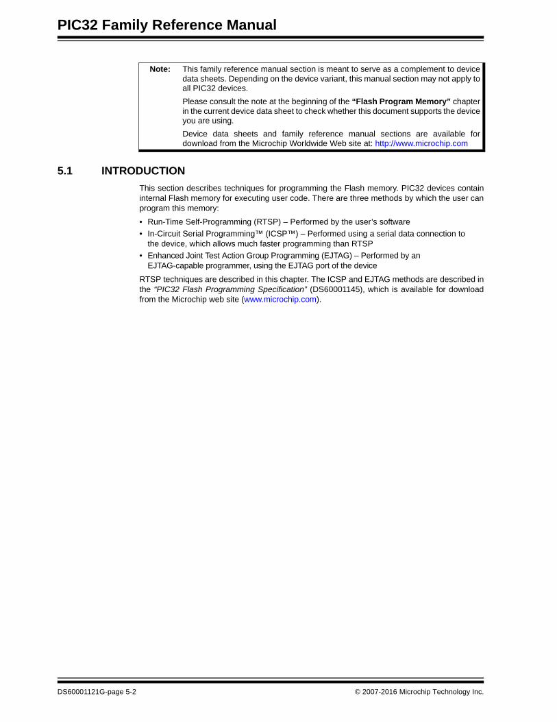
Note: This family reference manual section is meant to serve as a complement to devicedata sheets. Depending on the device variant, this manual section may not apply toall PIC32 devices.
Please consult the note at the beginning of the “Flash Program Memory” chapterin the current device data sheet to check whether this document supports the deviceyou are using.
Device data sheets and family reference manual sections are available fordownload from the Microchip Worldwide Web site at: http://www.microchip.com
DS60001121G-page 5-2 © 2007-2016 Microchip Technology Inc.
Section 5. Flash ProgrammingF
lash
P
rog
ramm
ing
5
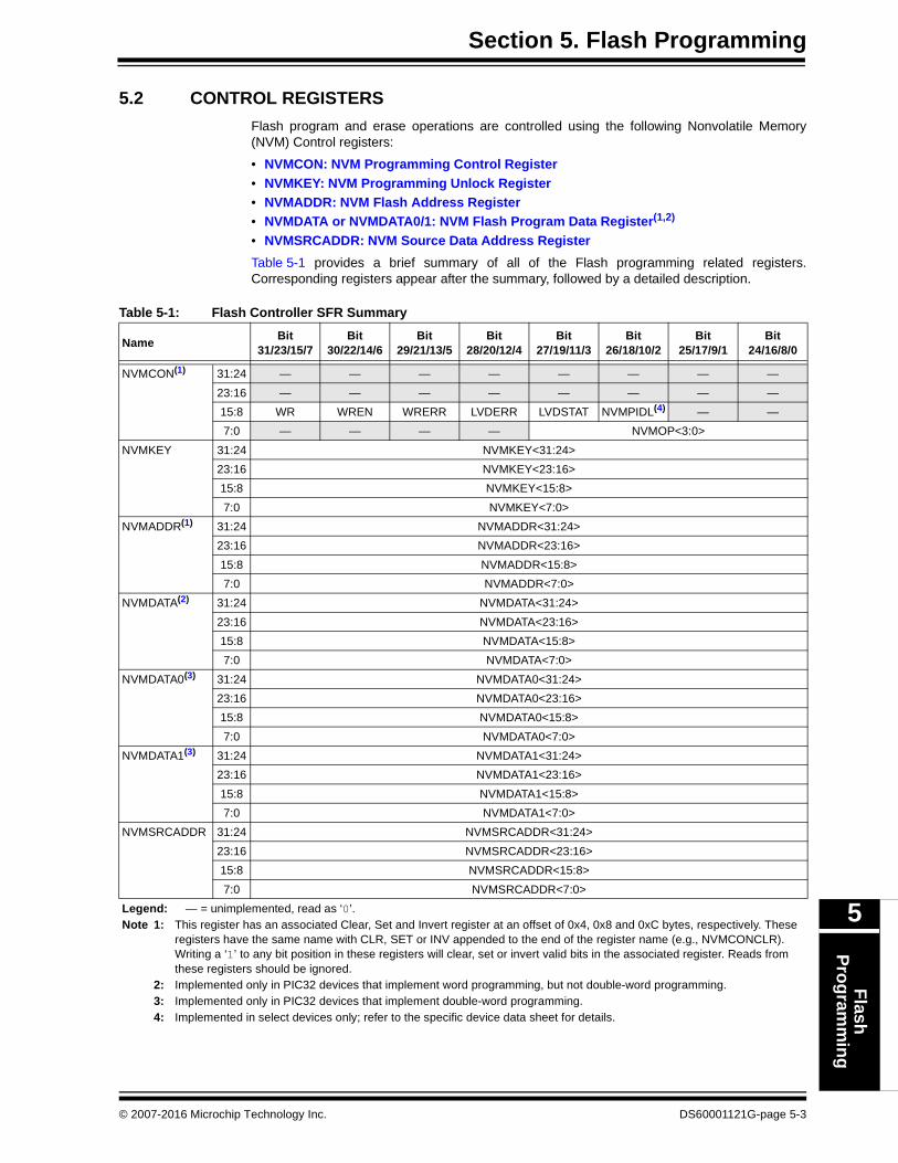
5.2 CONTROL REGISTERS
Flash program and erase operations are controlled using the following Nonvolatile Memory(NVM) Control registers:
• NVMCON: NVM Programming Control Register
• NVMKEY: NVM Programming Unlock Register
• NVMADDR: NVM Flash Address Register
• NVMDATA or NVMDATA0/1: NVM Flash Program Data Register(1,2)
• NVMSRCADDR: NVM Source Data Address Register
Table 5-1 provides a brief summary of all of the Flash programming related registers.Corresponding registers appear after the summary, followed by a detailed description.
Table 5-1: Flash Controller SFR Summary
NameBit
31/23/15/7Bit
30/22/14/6Bit
29/21/13/5Bit
28/20/12/4Bit
27/19/11/3Bit
26/18/10/2Bit
25/17/9/1Bit
24/16/8/0
NVMCON(1) 31:24 — — — — — — — —
23:16 — — — — — — — —
15:8 WR WREN WRERR LVDERR LVDSTAT NVMPIDL(4) — —
7:0 — — — — NVMOP<3:0>
NVMKEY 31:24 NVMKEY<31:24>
23:16 NVMKEY<23:16>
15:8 NVMKEY<15:8>
7:0 NVMKEY<7:0>
NVMADDR(1) 31:24 NVMADDR<31:24>
23:16 NVMADDR<23:16>
15:8 NVMADDR<15:8>
7:0 NVMADDR<7:0>
NVMDATA(2) 31:24 NVMDATA<31:24>
23:16 NVMDATA<23:16>
15:8 NVMDATA<15:8>
7:0 NVMDATA<7:0>
NVMDATA0(3) 31:24 NVMDATA0<31:24>
23:16 NVMDATA0<23:16>
15:8 NVMDATA0<15:8>
7:0 NVMDATA0<7:0>
NVMDATA1(3) 31:24 NVMDATA1<31:24>
23:16 NVMDATA1<23:16>
15:8 NVMDATA1<15:8>
7:0 NVMDATA1<7:0>
NVMSRCADDR 31:24 NVMSRCADDR<31:24>
23:16 NVMSRCADDR<23:16>
15:8 NVMSRCADDR<15:8>
7:0 NVMSRCADDR<7:0>
Legend: — = unimplemented, read as ‘0’.Note 1: This register has an associated Clear, Set and Invert register at an offset of 0x4, 0x8 and 0xC bytes, respectively. These
registers have the same name with CLR, SET or INV appended to the end of the register name (e.g., NVMCONCLR). Writing a ‘1’ to any bit position in these registers will clear, set or invert valid bits in the associated register. Reads from these registers should be ignored.
2: Implemented only in PIC32 devices that implement word programming, but not double-word programming.3: Implemented only in PIC32 devices that implement double-word programming.4: Implemented in select devices only; refer to the specific device data sheet for details.
© 2007-2016 Microchip Technology Inc. DS60001121G-page 5-3

PIC32 Family Reference Manual
5.2.1 NVMCON Register
The NVMCON register is the control register for Flash program/erase operations. This registerselects whether an erase or program operation can be performed and is used to start theprogram or erase cycle. The lower byte of NVMCON configures the type of NVM operation thatwill be performed. The register is shown in Register 5-1.
Register 5-1: NVMCON: NVM Programming Control Register
Bit Range
Bit31/23/15/7
Bit30/22/14/6
Bit29/21/13/5
Bit28/20/12/4
Bit27/19/11/3
Bit26/18/10/2
Bit25/17/9/1
Bit24/16/8/0
31:24U-0 U-0 U-0 U-0 U-0 U-0 U-0 U-0
— — — — — — — —
23:16U-0 U-0 U-0 U-0 U-0 U-0 U-0 U-0
— — — — — — — —
15:8R/W-0, HC R/W-0 R-0, HS R-0, HS R-0, HS, HC R-0, HS U-0 U-0
WR WREN(1) WRERR(2) LVDERR(2) LVDSTAT(2) NVMPIDL(2,3) — —
7:0U-0 U-0 U-0 U-0 R/W-0 R/W-0 R/W-0 R/W-0
— — — — NVMOP<3:0>
Legend: HS = Hardware Settable bit HC = Hardware Clearable bit
R = Readable bit W = Writable bit U = Unimplemented bit, read as ‘0’
-n = Value at POR ‘1’ = Bit is set ‘0’ = Bit is cleared x = Bit is unknown
bit 31-16 Unimplemented: Read as ‘0’
bit 15 WR: Write Control bit
This bit is writable when WREN = 1 and the unlock sequence is followed.1 = Initiates a Flash operation; hardware clears this bit when the operation completes0 = Flash operation is complete or inactive
bit 14 WREN: Write Enable bit(1)
1 = Enables writes to the WR bit and enables the Low-Voltage Detect (LVD) circuit0 = Disables writes to the WR bit and disables the LVD circuit
bit 13 WRERR: Write Error bit(2)
This bit is read-only and is automatically set by hardware.1 = Program or erase sequence did not complete successfully0 = Program or erase sequence completed normally
bit 12 LVDERR: Low-Voltage Detect Error bit (LVD circuit must be enabled)(2)
This bit is read-only and is automatically set by hardware.
1 = Low-voltage event detected (possible data corruption if WRERR is set)0 = Voltage level is acceptable for programming
bit 11 LVDSTAT: Low-Voltage Detect Status bit (LVD circuit must be enabled)(2)
This bit is read-only and is automatically set and cleared by hardware.1 = Low-voltage event is active0 = Low-voltage event is NOT active
bit 10 NVMPIDL: NVM Array Power-Down in Idle Enable bit(2,3)
1 = Power is removed from Flash memory when the device enters Idle mode0 = Power is maintained to Flash memory during Idle mode
bit 9-4 Unimplemented: Read as ‘0’
Note 1: This bit is reset by a device Reset.
2: This bit is cleared by setting NVMOP<3:0> = 0000 and initiating a Flash operation (i.e., WR).
3: Implemented in select devices only; refer to the specific device data sheet for details.
4: Operations are only valid if the page or address selected by NVMADDR is not write-protected.
DS60001121G-page 5-4 © 2007-2016 Microchip Technology Inc.
Section 5. Flash ProgrammingF
lash
P
rog
ramm
ing
5
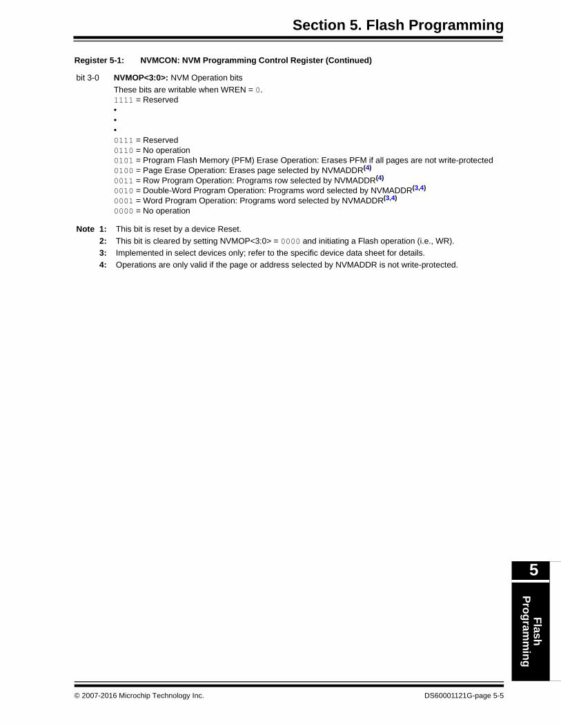
bit 3-0 NVMOP<3:0>: NVM Operation bits
These bits are writable when WREN = 0.1111 = Reserved•••0111 = Reserved0110 = No operation0101 = Program Flash Memory (PFM) Erase Operation: Erases PFM if all pages are not write-protected0100 = Page Erase Operation: Erases page selected by NVMADDR(4)
0011 = Row Program Operation: Programs row selected by NVMADDR(4)
0010 = Double-Word Program Operation: Programs word selected by NVMADDR(3,4)
0001 = Word Program Operation: Programs word selected by NVMADDR(3,4)
0000 = No operation
Register 5-1: NVMCON: NVM Programming Control Register (Continued)
Note 1: This bit is reset by a device Reset.
2: This bit is cleared by setting NVMOP<3:0> = 0000 and initiating a Flash operation (i.e., WR).
3: Implemented in select devices only; refer to the specific device data sheet for details.
4: Operations are only valid if the page or address selected by NVMADDR is not write-protected.
© 2007-2016 Microchip Technology Inc. DS60001121G-page 5-5

PIC32 Family Reference Manual
5.2.2 NVMKEY Register
NVMKEY is a write-only register that is used to prevent accidental writes/erasures of Flash orEEPROM memory. To start a programming or an erase sequence, the following steps must betaken in the exact order shown:
1. Write 0xAA996655 to NVMKEY.
2. Write 0x556699AA to NVMKEY.
After this sequence, only the next transaction on the peripheral bus is allowed to write to theNVMCON register. In most cases, the user will simply need to set the WR bit in the NVMCONregister to start the program or erase cycle. Interrupts should be disabled during the unlocksequence.
Register 5-2: NVMKEY: NVM Programming Unlock Register
Bit Range
Bit31/23/15/7
Bit30/22/14/6
Bit29/21/13/5
Bit28/20/12/4
Bit27/19/11/3
Bit26/18/10/2
Bit25/17/9/1
Bit24/16/8/0
31:24W-0 W-0 W-0 W-0 W-0 W-0 W-0 W-0
NVMKEY<31:24>
23:16W-0 W-0 W-0 W-0 W-0 W-0 W-0 W-0
NVMKEY<23:16>
15:8W-0 W-0 W-0 W-0 W-0 W-0 W-0 W-0
NVMKEY<15:8>
7:0W-0 W-0 W-0 W-0 W-0 W-0 W-0 W-0
NVMKEY<7:0>
Legend:
R = Readable bit W = Writable bit U = Unimplemented bit, read as ‘0’
-n = Value at POR ‘1’ = Bit is set ‘0’ = Bit is cleared x = Bit is unknown
bit 31-0 NVMKEY<31:0>: NVM Unlock Register bits
These bits are write-only and read as ‘0’ on any read.
DS60001121G-page 5-6 © 2007-2016 Microchip Technology Inc.
Section 5. Flash ProgrammingF
lash
P
rog
ramm
ing
5
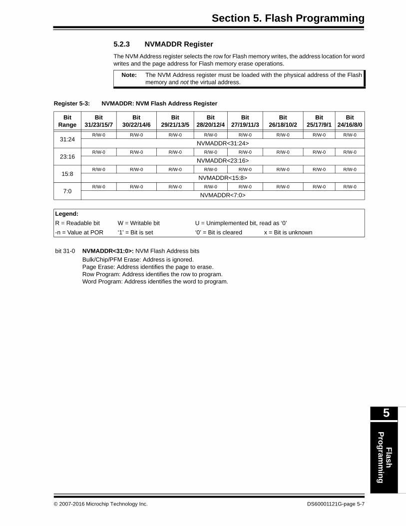
5.2.3 NVMADDR Register
The NVM Address register selects the row for Flash memory writes, the address location for wordwrites and the page address for Flash memory erase operations.
Note: The NVM Address register must be loaded with the physical address of the Flashmemory and not the virtual address.
Register 5-3: NVMADDR: NVM Flash Address Register
Bit Range
Bit31/23/15/7
Bit30/22/14/6
Bit29/21/13/5
Bit28/20/12/4
Bit27/19/11/3
Bit26/18/10/2
Bit25/17/9/1
Bit24/16/8/0
31:24R/W-0 R/W-0 R/W-0 R/W-0 R/W-0 R/W-0 R/W-0 R/W-0
NVMADDR<31:24>
23:16R/W-0 R/W-0 R/W-0 R/W-0 R/W-0 R/W-0 R/W-0 R/W-0
NVMADDR<23:16>
15:8R/W-0 R/W-0 R/W-0 R/W-0 R/W-0 R/W-0 R/W-0 R/W-0
NVMADDR<15:8>
7:0R/W-0 R/W-0 R/W-0 R/W-0 R/W-0 R/W-0 R/W-0 R/W-0
NVMADDR<7:0>
Legend:
R = Readable bit W = Writable bit U = Unimplemented bit, read as ‘0’
-n = Value at POR ‘1’ = Bit is set ‘0’ = Bit is cleared x = Bit is unknown
bit 31-0 NVMADDR<31:0>: NVM Flash Address bits
Bulk/Chip/PFM Erase: Address is ignored.Page Erase: Address identifies the page to erase.Row Program: Address identifies the row to program.Word Program: Address identifies the word to program.
© 2007-2016 Microchip Technology Inc. DS60001121G-page 5-7

PIC32 Family Reference Manual
5.2.4 NVMDATA Registers
The NVM Data registers hold the data to be programmed during Flash word program operations.Devices that implement only word and row programming implement a single register, NVMDATA.
Devices that implement double-word programming implement two registers, named NVMDATA0and NVMDATA1. In these devices, NVMDATA0 is used for the lower word of the data to bewritten in double-word operations.
Register 5-4: NVMDATA or NVMDATA0/1: NVM Flash Program Data Register(1,2)
Bit Range
Bit31/23/15/7
Bit30/22/14/6
Bit29/21/13/5
Bit28/20/12/4
Bit27/19/11/3
Bit26/18/10/2
Bit25/17/9/1
Bit24/16/8/0
31:24R/W-0 R/W-0 R/W-0 R/W-0 R/W-0 R/W-0 R/W-0 R/W-0
NVMDATA<31:24> or NVMDATA0/1<31:24>
23:16R/W-0 R/W-0 R/W-0 R/W-0 R/W-0 R/W-0 R/W-0 R/W-0
NVMDATA<23:16> or NVMDATA0/1<23:16>
15:8R/W-0 R/W-0 R/W-0 R/W-0 R/W-0 R/W-0 R/W-0 R/W-0
NVMDATA<15:8> or NVMDATA0/1<15:8>
7:0R/W-0 R/W-0 R/W-0 R/W-0 R/W-0 R/W-0 R/W-0 R/W-0
NVMDATA<7:0> or NVMDATA0/1<7:0>
Legend:
R = Readable bit W = Writable bit U = Unimplemented bit, read as ‘0’
-n = Value at POR ‘1’ = Bit is set ‘0’ = Bit is cleared x = Bit is unknown
bit 31-0 NVMDATA<31:0>: NVM Flash Programming Data bits
NVMDATA0<31:0>: NVM Flash Programming Data bits (lower word, select devices only)
NVMDATA1<31:0>: NVM Flash Programming Data bits (upper word, select devices only)
Note 1: The name and number of registers implemented is device-specific. Refer to the device data sheet for more information.
2: This register is reset only on a Power-on Reset (POR).
DS60001121G-page 5-8 © 2007-2016 Microchip Technology Inc.

Section 5. Flash ProgrammingF
lash
P
rog
ramm
ing
5
5.2.5 NVMSRCADDR Register
The NVM Source Data Address register selects the source data buffer address in SRAM forperforming row programming operations.
Note: The address must be word-aligned.
Register 5-5: NVMSRCADDR: NVM Source Data Address Register
Bit Range
Bit31/23/15/7
Bit30/22/14/6
Bit29/21/13/5
Bit28/20/12/4
Bit27/19/11/3
Bit26/18/10/2
Bit25/17/9/1
Bit24/16/8/0
31:24R/W-0 R/W-0 R/W-0 R/W-0 R/W-0 R/W-0 R/W-0 R/W-0
NVMSRCADDR<31:24>
23:16R/W-0 R/W-0 R/W-0 R/W-0 R/W-0 R/W-0 R/W-0 R/W-0
NVMSRCADDR<23:16>
15:8R/W-0 R/W-0 R/W-0 R/W-0 R/W-0 R/W-0 R/W-0 R/W-0
NVMSRCADDR<15:8>
7:0R/W-0 R/W-0 R/W-0 R/W-0 R/W-0 R/W-0 R/W-0 R/W-0
NVMSRCADDR<7:0>
Legend:
R = Readable bit W = Writable bit U = Unimplemented bit, read as ‘0’
-n = Value at POR ‘1’ = Bit is set ‘0’ = Bit is cleared x = Bit is unknown
bit 31-0 NVMSRCADDR<31:0>: NVM Source Data Address bits
The system physical address of the data to be programmed into the Flash when the NVMOP<3:0> bits(NVMCON<3:0>) are set to perform row programming.
© 2007-2016 Microchip Technology Inc. DS60001121G-page 5-9

PIC32 Family Reference Manual
5.3 RUN-TIME SELF-PROGRAMMING (RTSP) OPERATION
Run-Time Self-Programming (RTSP) allows the user code to modify Flash program memorycontents. The device Flash memory is divided into two logical Flash partitions: the Program FlashMemory (PFM) and the Boot Flash Memory (BFM). The last page in Boot Flash Memory containsthe debug page, which is reserved for use by the debugger tool while debugging.
The program Flash array for the PIC32 device is built up of a series of rows to form a page. Referto the “Flash Program Memory” chapter of the specific device data sheet to determine the rowand page sizes. For example, a row may contain 128 32-bit instruction words or 512 bytes. Agroup of 8 rows compose a page; which, therefore, contains 8 × 512 = 4096 bytes or1024 instruction words. A page of Flash is the smallest unit of memory that can be erased at asingle time. The program Flash array can be programmed in several ways:
• Word Programming, with 1 instruction word at a time (most devices)
• Double-Word Programming, with 2 instruction words at a time (select devices only)
• Row Programming, with 64 or 128 instruction words at a time
Performing an RTSP operation while executing (fetching) instructions from Program FlashMemory causes the CPU to stall (wait) until the programming operation is finished. The CPU willnot execute any instruction, or respond to interrupts, during this time. If any interrupts occurduring the programming cycle, they remain pending until the cycle completes.
If performing an RTSP operation while executing (fetching) instructions from RAM memory, theCPU can continue to execute instructions and respond to interrupts during the programmingoperation. Any executable code scheduled to execute during the RTSP operation must be placedin RAM memory; this includes the relevant interrupt vector and the Interrupt Service Routine(ISR) instructions.
Note: A minimum VDD requirement for Flash erase and write operations is required. Referto the “Electrical Characteristics” chapter in the specific device data sheet formore information.
DS60001121G-page 5-10 © 2007-2016 Microchip Technology Inc.

Section 5. Flash ProgrammingF
lash
P
rog
ramm
ing
5
5.4 LOCK-OUT FEATURE
5.4.1 NVM WREN
A number of mechanisms exists within the device to ensure that inadvertent writes to programFlash do not occur. The WREN bit (NVMCON<14>) should be zero unless the software intendsto write to the program Flash. When WREN = 1, the Flash Write Control bit, WR(NVMCON<15>), is writable and the Flash LVD circuit is enabled.
5.4.2 NVMKEY
In addition to the write protection provided by the WREN bit, an unlock sequence needs to beperformed before the WR bit (NVMCOM<15>) can be set. If the WR bit is not set on the nextperipheral bus transaction (read or write), WR is locked and the unlock sequence must berestarted.
5.4.3 Unlock Sequence
To unlock Flash operations, perform Steps 4 through 8 in order. If the sequence is not followed,WR is not set.
1. Suspend or disable all initiators that can access the peripheral bus and interrupt theunlock sequence (e.g., DMA and interrupts).
2. Set the WREN bit (NVMCON<14>) to allow writes to WR and set the NVMOP<3:0> bits(NVMCON<3:0>) to the desired operation with a single store instruction.
3. Wait for LVD to start-up.
4. Load 0xAA996655 to CPU Register X.
5. Load 0x556699AA to CPU Register Y.
6. Load 0x00008000 to CPU Register Z.
7. Store CPU Register X to NVMKEY.
8. Store CPU Register Y to NVMKEY.
9. Store CPU Register Z to NVMCONSET.
10. Wait for the WR bit (NVMCON<15>) to be cleared.
11. Clear the WREN bit (NVMCON<14>).
12. Check the WRERR (NVMCON<13>) and LVDERR (NVMCON<12>) bits to ensure thatthe program/erase sequence completed successfully.
When the WR bit is set, the program/erase sequence starts and the CPU is unable to executefrom Flash memory for the duration of the sequence.
© 2007-2016 Microchip Technology Inc. DS60001121G-page 5-11

PIC32 Family Reference Manual
Example 5-1: Unlock Example
unsigned int NVMUnlock (unsigned int nvmop){
unsigned int status;
// Suspend or Disable all Interruptsasm volatile (“di %0” : “=r” (status));
// Enable Flash Write/Erase Operations and Select// Flash operation to performNVMCON = nvmop;
// Write KeysNVMKEY = 0xAA996655;NVMKEY = 0x556699AA;
// Start the operation using the Set RegisterNVMCONSET = 0x8000;
// Wait for operation to completewhile (NVMCON & 0x8000);
// Restore Interruptsif (status & 0x00000001)asm volatile (“ei”);elseasm volatile (“di”);
// Disable NVM write enableNVMCONCLR = 0x0004000;
// Return WRERR and LVDERR Error Status Bits return (NVMCON & 0x3000);
}
DS60001121G-page 5-12 © 2007-2016 Microchip Technology Inc.

Section 5. Flash ProgrammingF
lash
P
rog
ramm
ing
5
5.5 WORD PROGRAMMING SEQUENCE
The smallest block of data that can be programmed in a single operation is one 32-bit word. Thedata to be programmed must be written to the NVMDATA register and the address of the wordmust be loaded into the NVMADDR register before the programming sequence is initiated. Theinstruction word at the location pointed to by the NVMADDR register is then programmed.
A program sequence comprises the following steps:
1. Write 32-bit data to be programmed to the NVMDATA register.
2. Load the NVMADDR register with the address to be programmed.
3. Run the unlock sequence using the word program command (see Section 5.4.3 “UnlockSequence”).
The program sequence completes and the WR bit (NVMCON<15>) is cleared by hardware.
Example 5-2: Word Program Example
5.6 DOUBLE-WORD PROGRAMMING SEQUENCE
Double-word programming follows essentially the same sequence as word programming, exceptthat the data is written to two NVMDATA registers. In this scenario, the lower word of data iswritten to NVMDATA0 and the upper word to NVMDATA1.
A program sequence comprises the following steps:
1. Write 64-bit data to be programmed to the NVMDATA0 and NVMDATA1 registers.
2. Load the NVMADDR register with the address to be programmed.
3. Run the unlock sequence using the word program command (see Section 5.4.3 “UnlockSequence”).
The program sequence completes and the WR bit (NVMCON<15>) is cleared by hardware.
Example 5-3: Word Program Example
unsigned int NVMWriteWord (void* address, unsigned int data){
unsigned int res;
// Load data into NVMDATA registerNVMDATA = data;// Load address to program into NVMADDR registerNVMADDR = (unsigned int) address;// Unlock and Write Wordres = NVMUnlock (0x4001);// Return Resultreturn res;
}
unsigned int NVMWriteWord (void* address, unsigned int data){
unsigned int res;
// Load data into NVMDATA registerNVMDATA0 = data_l;NVMDATA1 = data_h;// Load address to program into NVMADDR registerNVMADDR = (unsigned int) address;// Unlock and Write Wordres = NVMUnlock (0x4010);// Return Resultreturn res;
}
© 2007-2016 Microchip Technology Inc. DS60001121G-page 5-13
PIC32 Family Reference Manual
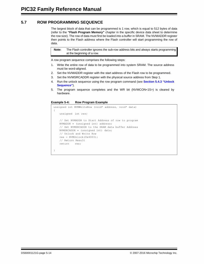
5.7 ROW PROGRAMMING SEQUENCE
The largest block of data that can be programmed is 1 row, which is equal to 512 bytes of data(refer to the “Flash Program Memory” chapter in the specific device data sheet to determinethe row size). The row of data must first be loaded into a buffer in SRAM. The NVMADDR registerthen points to the Flash address where the Flash controller will start programming the row ofdata.
A row program sequence comprises the following steps:
1. Write the entire row of data to be programmed into system SRAM. The source addressmust be word-aligned.
2. Set the NVMADDR register with the start address of the Flash row to be programmed.
3. Set the NVMSRCADDR register with the physical source address from Step 1.
4. Run the unlock sequence using the row program command (see Section 5.4.3 “UnlockSequence”).
5. The program sequence completes and the WR bit (NVMCON<15>) is cleared byhardware.
Example 5-4: Row Program Example
Note: The Flash controller ignores the sub-row address bits and always starts programmingat the beginning of a row.
unsigned int NVMWriteRow (void* address, void* data){
unsigned int res;
// Set NVMADDR to Start Address of row to programNVMADDR = (unsigned int) address;// Set NVMSRCADDR to the SRAM data buffer AddressNVMSRCADDR = (unsigned int) data;// Unlock and Write Rowres = NVMUnlock(0x4003);// Return Resultreturn res;
}
DS60001121G-page 5-14 © 2007-2016 Microchip Technology Inc.
Section 5. Flash ProgrammingF
lash
P
rog
ramm
ing
5
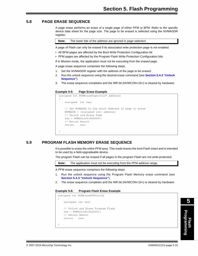
5.8 PAGE ERASE SEQUENCE
A page erase performs an erase of a single page of either PFM or BFM. Refer to the specificdevice data sheet for the page size. The page to be erased is selected using the NVMADDRregister.
A page of Flash can only be erased if its associated write protection page is not enabled.
• All BFM pages are affected by the Boot Write Protection Configuration bit
• PFM pages are affected by the Program Flash Write Protection Configuration bits
If in Mission mode, the application must not be executing from the erased page.
A page erase sequence comprises the following steps:
1. Set the NVMADDR register with the address of the page to be erased.
2. Run the unlock sequence using the desired erase command (see Section 5.4.3 “UnlockSequence”).
3. The erase sequence completes and the WR bit (NVMCON<15>) is cleared by hardware.
Example 5-5: Page Erase Example
5.9 PROGRAM FLASH MEMORY ERASE SEQUENCE
It is possible to erase the entire PFM area. This mode leaves the boot Flash intact and is intendedto be used by a field-upgradeable device.
The program Flash can be erased if all pages in the program Flash are not write-protected.
A PFM erase sequence comprises the following steps:
1. Run the unlock sequence using the Program Flash Memory erase command (seeSection 5.4.3 “Unlock Sequence”).
2. The erase sequence completes and the WR bit (NVMCON<15>) is cleared by hardware.
Example 5-6: Program Flash Erase Example
Note: The lower bits of the address are ignored in page selection.
unsigned int NVMErasePage(void* address){
unsigned int res;
// Set NVMADDR to the Start Address of page to eraseNVMADDR = (unsigned int) address;// Unlock and Erase Pageres = NVMUnlock(0x4004);// Return Resultreturn res;
}
Note: The application must not be executing from the PFM address range.
unsigned int NVMErasePFM(void){
unsigned int res;
// Unlock and Erase Program Flashres = NVMUnlock(0x4005);// Return Resultreturn res;
}
© 2007-2016 Microchip Technology Inc. DS60001121G-page 5-15
PIC32 Family Reference Manual
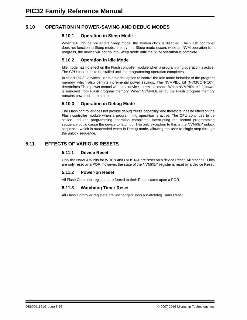
5.10 OPERATION IN POWER-SAVING AND DEBUG MODES
5.10.1 Operation in Sleep Mode
When a PIC32 device enters Sleep mode, the system clock is disabled. The Flash controllerdoes not function in Sleep mode. If entry into Sleep mode occurs while an NVM operation is inprogress, the device will not go into Sleep mode until the NVM operation is complete.
5.10.2 Operation in Idle Mode
Idle mode has no effect on the Flash controller module when a programming operation is active.The CPU continues to be stalled until the programming operation completes.
In select PIC32 devices, users have the option to control the Idle mode behavior of the programmemory, which also permits incremental power savings. The NVMPIDL bit (NVMCON<10>)determines Flash power control when the device enters Idle mode. When NVMPIDL is ‘1’, poweris removed from Flash program memory. When NVMPIDL is ‘0’, the Flash program memoryremains powered in Idle mode.
5.10.3 Operation in Debug Mode
The Flash controller does not provide debug freeze capability, and therefore, has no effect on theFlash controller module when a programming operation is active. The CPU continues to bestalled until the programming operation completes. Interrupting the normal programmingsequence could cause the device to latch up. The only exception to this is the NVMKEY unlocksequence, which is suspended when in Debug mode, allowing the user to single step throughthe unlock sequence.
5.11 EFFECTS OF VARIOUS RESETS
5.11.1 Device Reset
Only the NVMCON bits for WREN and LVDSTAT are reset on a device Reset. All other SFR bitsare only reset by a POR; however, the state of the NVMKEY register is reset by a device Reset.
5.11.2 Power-on Reset
All Flash Controller registers are forced to their Reset states upon a POR.
5.11.3 Watchdog Timer Reset
All Flash Controller registers are unchanged upon a Watchdog Timer Reset.
DS60001121G-page 5-16 © 2007-2016 Microchip Technology Inc.

Section 5. Flash ProgrammingF
lash
P
rog
ramm
ing
5
5.12 INTERRUPTS
The Flash controller can generate an interrupt reflecting the events that occur during theprogramming operations. The following interrupts can be generated:
• Flash Control Event Interrupt Flag (FCEIF)
The interrupt flag must be cleared in software.The Flash controller is enabled as a source ofinterrupt via the following bit:
• Flash Controller Event Interrupt Enable (FCEIE)
The Interrupt Priority Level (IPL) bits and interrupt subpriority level bits must also be configured:
• FCEIP<2:0>
• FCEIS<1:0>
Refer to Section 8. “Interrupts” (DS60001108) in the “PIC32 Family Reference Manual” fordetails.
5.12.1 Interrupt Configuration
The Flash controller module has a dedicated interrupt flag bit, FCEIF, and a correspondinginterrupt enable/mask bit, FCEIE.
These two bits determine the source of an interrupt and enable or disable an individual interruptsource. All the interrupt sources for a specific Flash controller module share one interrupt vector.
In addition, the FCEIF bit will be set without regard to the state of the corresponding enable bitand the FCEIF bit can be polled by software if desired.
The FCEIE bit is used to define the behavior of the Vector Interrupt Controller (VIC) when acorresponding FCEIF bit is set. When the corresponding FCEIE bit is clear, the VIC module doesnot generate a CPU interrupt for the event. If the FCEIE bit is set, the VIC module will generatean interrupt to the CPU when the corresponding FCEIF bit is set (subject to the priority andsubpriority as outlined in the following paragraphs).
It is the responsibility of the user’s software routine that services a particular interrupt to clear theappropriate interrupt flag bit before the service routine is complete.
The priority of the Flash controller module can be set independently with the FCEIP<2:0> bits.This priority defines the priority group to which the interrupt source is assigned. The prioritygroups range from a value of 7 (the highest priority) to a value of 0, which does not generate aninterrupt. An interrupt being serviced is preempted by an interrupt in a higher priority group.
The subpriority bits allow setting the priority of a interrupt source within a priority group. Thevalues of the subpriority bits, FCEIS<1:0>, range from 3 (the highest priority) to 0 (the lowestpriority). An interrupt with the same priority group, but having a higher subpriority value does notpreempt a lower subpriority interrupt that is in progress.
The priority group and subpriority bits allow more than one interrupt source to share the samepriority and subpriority. If simultaneous interrupts occur in this configuration, the natural order ofthe interrupt sources within a priority/subpriority group pair determine the interrupt generated.The natural priority is based on the vector numbers of the interrupt sources. The lower the vectornumber, the higher the natural priority of the interrupt. Any interrupts that are overridden bynatural order generate their respective interrupts based on priority, subpriority and natural order,after the interrupt flag for the current interrupt is cleared.
After an enabled interrupt is generated, the CPU jumps to the vector assigned to that interrupt.The vector number for the interrupt is the same as the natural order number. Then, the CPUbegins executing code at the vector address. The user’s code at this vector address shouldperform any application-specific operations, clear the FCEIF interrupt flag and then exit.
For more information on interrupts and the vector address table details, refer to Section 8.“Interrupts” (DS60001108) in the “PIC32 Family Reference Manual” and the “InterruptController” chapter of the specific device data sheet.
© 2007-2016 Microchip Technology Inc. DS60001121G-page 5-17
PIC32 Family Reference Manual
5.13 RELATED APPLICATION NOTES
This section lists application notes that are related to this section of the manual. Theseapplication notes may not be written specifically for the PIC32 device family, but the concepts arepertinent and could be used with modification and possible limitations. The current applicationnotes related to Flash Programming include the following:
Title Application Note #
No related application notes at this time. N/A
Note: Please visit the Microchip web site (www.microchip.com) for additional applicationnotes and code examples for the PIC32 family of devices.
DS60001121G-page 5-18 © 2007-2016 Microchip Technology Inc.
Section 5. Flash ProgrammingF
lash
P
rog
ramm
ing
5
5.14 REVISION HISTORY
Revision A (September 2007)
This is the initial released version of this document.
Revision B (October 2007)
Updated document to remove Confidential status.
Revision C (April 2008)
Revised status to Preliminary; revised U-0 to r-x.
Revision D (June 2008)
Revised Register 5-1, bit 14 NVMWREN. Added footnote 1 to Registers 5-12 through 5-14.Added note to Section 5.3. Revised Section 5.4.1. Revised Example 5-1. Changed Reserved bitsfrom “Maintain as” to “Write”.
Revision E (December 2010)
This revision includes the following updates:
• Minor updates to the text and formatting have been incorporated throughout the document
• Added Notes 1, 2 and 3, which describe the Clear, Set and Invert registers to the following:
- Table 5-1: Flash Controller SFR Summary
- Register 5-1: NVMCON: NVM Programming Control Register(1,2,3)
- Register 5-3: NVMADDR: NVM Flash Address Register(1,2,3)
• Removed all Clear, Set and Invert register descriptions
• Removed all Interrupt register references
• The following NVMCON register bit names were changed throughout the document:
- NVMWR was renamed to WR
- NVMWREN was renamed to WREN
- NVMERR was renamed to WRERR
• Updated the third paragraph and added a new (fourth) paragraph to Section 5.3 “Run-Time Self-Programming (RTSP) Operation”
• Updated the unlock Flash operations sequence by adding a new Step 3 (see Section 5.4.3 “Unlock Sequence”)
• Updated the code in the Unlock Example (see Example 5-1)
• Removed Table 5-3
Revision F (July 2012)
This revision includes the following updates:
• Updated Note 1 and removed Notes 2 and 3 from the Flash Controller SFR Register Summary (see Table 5-1)
• Updated the NVMCON register (see Register 5-1)
• Removed Notes 1, 2 and 3 from NVMADDR (see Register 5-3)
• Updated the second paragraph of Section 5.3 “Run-Time Self-Programming (RTSP) Operation”
• Updated the first paragraph of Section 5.7 “Row Programming Sequence”
• Updated the first paragraph of Section 5.8 “Page Erase Sequence”
• Minor updates to the text and formatting have been incorporated throughout the document
© 2007-2016 Microchip Technology Inc. DS60001121G-page 5-19
PIC32 Family Reference Manual
Revision G (March 2016)
Added double-word programming:
• Added the NVMPIDL bit and supporting footnotes to NVMCON<10>; also defines a combinatorial for double-word programming (and supporting footnotes) to NVMCON<3:0>.
• Added NVMDATA0 and 1 registers to Table 5-1.
• Updated Section 5.2.4 “NVMDATA Registers” to add descriptions for NVMDATA0 and 1 registers.
• Updated Section 5.3 “Run-Time Self-Programming (RTSP) Operation” to add a description for double-word programming.
• Added Section 5.6 “Double-Word Programming Sequence”; all subsequent sections are renumbered accordingly.
• Amended Section 5.10.2 “Operation in Idle Mode” to include a description of the NVMPIDL bit’s functionality.
• Other minor typographic corrections throughout the document.
DS60001121G-page 5-20 © 2007-2016 Microchip Technology Inc.
Note the following details of the code protection feature on Microchip devices:
• Microchip products meet the specification contained in their particular Microchip Data Sheet.
• Microchip believes that its family of products is one of the most secure families of its kind on the market today, when used in the intended manner and under normal conditions.
• There are dishonest and possibly illegal methods used to breach the code protection feature. All of these methods, to our knowledge, require using the Microchip products in a manner outside the operating specifications contained in Microchip’s Data Sheets. Most likely, the person doing so is engaged in theft of intellectual property.
• Microchip is willing to work with the customer who is concerned about the integrity of their code.
• Neither Microchip nor any other semiconductor manufacturer can guarantee the security of their code. Code protection does not mean that we are guaranteeing the product as “unbreakable.”
Code protection is constantly evolving. We at Microchip are committed to continuously improving the code protection features of ourproducts. Attempts to break Microchip’s code protection feature may be a violation of the Digital Millennium Copyright Act. If such actsallow unauthorized access to your software or other copyrighted work, you may have a right to sue for relief under that Act.
Information contained in this publication regarding deviceapplications and the like is provided only for your convenienceand may be superseded by updates. It is your responsibility toensure that your application meets with your specifications.MICROCHIP MAKES NO REPRESENTATIONS ORWARRANTIES OF ANY KIND WHETHER EXPRESS ORIMPLIED, WRITTEN OR ORAL, STATUTORY OROTHERWISE, RELATED TO THE INFORMATION,INCLUDING BUT NOT LIMITED TO ITS CONDITION,QUALITY, PERFORMANCE, MERCHANTABILITY ORFITNESS FOR PURPOSE. Microchip disclaims all liabilityarising from this information and its use. Use of Microchipdevices in life support and/or safety applications is entirely atthe buyer’s risk, and the buyer agrees to defend, indemnify andhold harmless Microchip from any and all damages, claims,suits, or expenses resulting from such use. No licenses areconveyed, implicitly or otherwise, under any Microchipintellectual property rights unless otherwise stated.
2007-2016 Microchip Technology Inc.
Microchip received ISO/TS-16949:2009 certification for its worldwide headquarters, design and wafer fabrication facilities in Chandler and Tempe, Arizona; Gresham, Oregon and design centers in California and India. The Company’s quality system processes and procedures are for its PIC® MCUs and dsPIC® DSCs, KEELOQ® code hopping devices, Serial EEPROMs, microperipherals, nonvolatile memory and analog products. In addition, Microchip’s quality system for the design and manufacture of development systems is ISO 9001:2000 certified.
QUALITY MANAGEMENT SYSTEM CERTIFIED BY DNV
== ISO/TS 16949 ==
Trademarks
The Microchip name and logo, the Microchip logo, AnyRate, dsPIC, FlashFlex, flexPWR, Heldo, JukeBlox, KeeLoq, KeeLoq logo, Kleer, LANCheck, LINK MD, MediaLB, MOST, MOST logo, MPLAB, OptoLyzer, PIC, PICSTART, PIC32 logo, RightTouch, SpyNIC, SST, SST Logo, SuperFlash and UNI/O are registered trademarks of Microchip Technology Incorporated in the U.S.A. and other countries.
ClockWorks, The Embedded Control Solutions Company, ETHERSYNCH, Hyper Speed Control, HyperLight Load, IntelliMOS, mTouch, Precision Edge, and QUIET-WIRE are registered trademarks of Microchip Technology Incorporated in the U.S.A.
Analog-for-the-Digital Age, Any Capacitor, AnyIn, AnyOut, BodyCom, chipKIT, chipKIT logo, CodeGuard, dsPICDEM, dsPICDEM.net, Dynamic Average Matching, DAM, ECAN, EtherGREEN, In-Circuit Serial Programming, ICSP, Inter-Chip Connectivity, JitterBlocker, KleerNet, KleerNet logo, MiWi, motorBench, MPASM, MPF, MPLAB Certified logo, MPLIB, MPLINK, MultiTRAK, NetDetach, Omniscient Code Generation, PICDEM, PICDEM.net, PICkit, PICtail, PureSilicon, RightTouch logo, REAL ICE, Ripple Blocker, Serial Quad I/O, SQI, SuperSwitcher, SuperSwitcher II, Total Endurance, TSHARC, USBCheck, VariSense, ViewSpan, WiperLock, Wireless DNA, and ZENA are trademarks of Microchip Technology Incorporated in the U.S.A. and other countries.
SQTP is a service mark of Microchip Technology Incorporated in the U.S.A.
Silicon Storage Technology is a registered trademark of Microchip Technology Inc. in other countries.
GestIC is a registered trademarks of Microchip Technology Germany II GmbH & Co. KG, a subsidiary of Microchip Technology Inc., in other countries.
All other trademarks mentioned herein are property of their respective companies.
© 2007-2016, Microchip Technology Incorporated, Printed in the U.S.A., All Rights Reserved.
ISBN: 978-1-5224-0424-8
DS60001121G-page 5-21
DS60001121G-page 5-22 2007-2016 Microchip Technology Inc.
AMERICASCorporate Office2355 West Chandler Blvd.Chandler, AZ 85224-6199Tel: 480-792-7200 Fax: 480-792-7277Technical Support: http://www.microchip.com/supportWeb Address: www.microchip.com
AtlantaDuluth, GA Tel: 678-957-9614 Fax: 678-957-1455
Austin, TXTel: 512-257-3370
BostonWestborough, MA Tel: 774-760-0087 Fax: 774-760-0088
ChicagoItasca, IL Tel: 630-285-0071 Fax: 630-285-0075
ClevelandIndependence, OH Tel: 216-447-0464 Fax: 216-447-0643
DallasAddison, TX Tel: 972-818-7423 Fax: 972-818-2924
DetroitNovi, MI Tel: 248-848-4000
Houston, TX Tel: 281-894-5983
IndianapolisNoblesville, IN Tel: 317-773-8323Fax: 317-773-5453
Los AngelesMission Viejo, CA Tel: 949-462-9523 Fax: 949-462-9608
New York, NY Tel: 631-435-6000
San Jose, CA Tel: 408-735-9110
Canada - TorontoTel: 905-673-0699 Fax: 905-673-6509
ASIA/PACIFICAsia Pacific OfficeSuites 3707-14, 37th FloorTower 6, The GatewayHarbour City, Kowloon
Hong KongTel: 852-2943-5100Fax: 852-2401-3431
Australia - SydneyTel: 61-2-9868-6733Fax: 61-2-9868-6755
China - BeijingTel: 86-10-8569-7000 Fax: 86-10-8528-2104
China - ChengduTel: 86-28-8665-5511Fax: 86-28-8665-7889
China - ChongqingTel: 86-23-8980-9588Fax: 86-23-8980-9500
China - DongguanTel: 86-769-8702-9880
China - HangzhouTel: 86-571-8792-8115 Fax: 86-571-8792-8116
China - Hong Kong SARTel: 852-2943-5100 Fax: 852-2401-3431
China - NanjingTel: 86-25-8473-2460Fax: 86-25-8473-2470
China - QingdaoTel: 86-532-8502-7355Fax: 86-532-8502-7205
China - ShanghaiTel: 86-21-5407-5533 Fax: 86-21-5407-5066
China - ShenyangTel: 86-24-2334-2829Fax: 86-24-2334-2393
China - ShenzhenTel: 86-755-8864-2200 Fax: 86-755-8203-1760
China - WuhanTel: 86-27-5980-5300Fax: 86-27-5980-5118
China - XianTel: 86-29-8833-7252Fax: 86-29-8833-7256
ASIA/PACIFICChina - XiamenTel: 86-592-2388138 Fax: 86-592-2388130
China - ZhuhaiTel: 86-756-3210040 Fax: 86-756-3210049
India - BangaloreTel: 91-80-3090-4444 Fax: 91-80-3090-4123
India - New DelhiTel: 91-11-4160-8631Fax: 91-11-4160-8632
India - PuneTel: 91-20-3019-1500
Japan - OsakaTel: 81-6-6152-7160 Fax: 81-6-6152-9310
Japan - TokyoTel: 81-3-6880- 3770 Fax: 81-3-6880-3771
Korea - DaeguTel: 82-53-744-4301Fax: 82-53-744-4302
Korea - SeoulTel: 82-2-554-7200Fax: 82-2-558-5932 or 82-2-558-5934
Malaysia - Kuala LumpurTel: 60-3-6201-9857Fax: 60-3-6201-9859
Malaysia - PenangTel: 60-4-227-8870Fax: 60-4-227-4068
Philippines - ManilaTel: 63-2-634-9065Fax: 63-2-634-9069
SingaporeTel: 65-6334-8870Fax: 65-6334-8850
Taiwan - Hsin ChuTel: 886-3-5778-366Fax: 886-3-5770-955
Taiwan - KaohsiungTel: 886-7-213-7828
Taiwan - TaipeiTel: 886-2-2508-8600 Fax: 886-2-2508-0102
Thailand - BangkokTel: 66-2-694-1351Fax: 66-2-694-1350
EUROPEAustria - WelsTel: 43-7242-2244-39Fax: 43-7242-2244-393
Denmark - CopenhagenTel: 45-4450-2828 Fax: 45-4485-2829
France - ParisTel: 33-1-69-53-63-20 Fax: 33-1-69-30-90-79
Germany - DusseldorfTel: 49-2129-3766400
Germany - KarlsruheTel: 49-721-625370
Germany - MunichTel: 49-89-627-144-0 Fax: 49-89-627-144-44
Italy - Milan Tel: 39-0331-742611 Fax: 39-0331-466781
Italy - VeniceTel: 39-049-7625286
Netherlands - DrunenTel: 31-416-690399 Fax: 31-416-690340
Poland - WarsawTel: 48-22-3325737
Spain - MadridTel: 34-91-708-08-90Fax: 34-91-708-08-91
Sweden - StockholmTel: 46-8-5090-4654
UK - WokinghamTel: 44-118-921-5800Fax: 44-118-921-5820
Worldwide Sales and Service
07/14/15