section i - technologydownload.beckhoff.com/download/document/io/ethercat...section i deals with the...
TRANSCRIPT

Version 2.2 Date: 2014-07-07
Hardware Data Sheet Section I
Slave Controller Section I – Technology EtherCAT Protocol, Physical Layer,
EtherCAT Processing Unit, FMMU, SyncManager, SII EEPROM, Distributed Clocks
Section II – Register Description (Online at http://www.beckhoff.com)
Section III – Hardware Description (Online at http://www.beckhoff.com)

DOCUMENT ORGANIZATION
I-II Slave Controller – Technology
DOCUMENT ORGANIZATION
The Beckhoff EtherCAT Slave Controller (ESC) documentation covers the following Beckhoff ESCs:
ET1200
ET1100
EtherCAT IP Core for Altera® FPGAs
EtherCAT IP Core for Xilinx® FPGAs
ESC20
The documentation is organized in three sections. Section I and section II are common for all Beckhoff ESCs, Section III is specific for each ESC variant.
The latest documentation is available at the Beckhoff homepage (http://www.beckhoff.com).
Section I – Technology (All ESCs)
Section I deals with the basic EtherCAT technology. Starting with the EtherCAT protocol itself, the frame processing inside EtherCAT slaves is described. The features and interfaces of the physical layer with its two alternatives Ethernet and EBUS are explained afterwards. Finally, the details of the functional units of an ESC like FMMU, SyncManager, Distributed Clocks, Slave Information Interface, Interrupts, Watchdogs, and so on, are described.
Since Section I is common for all Beckhoff ESCs, it might describe features which are not available in a specific ESC. Refer to the feature details overview in Section III of a specific ESC to find out which features are available.
Section II – Register Description (All ESCs)
Section II contains detailed information about all ESC registers. This section is also common for all Beckhoff ESCs, thus registers, register bits, or features are described which might not be available in a specific ESC. Refer to the register overview and to the feature details overview in Section III of a specific ESC to find out which registers and features are available.
Section III – Hardware Description (Specific ESC)
Section III is ESC specific and contains detailed information about the ESC features, implemented registers, configuration, interfaces, pinout, usage, electrical and mechanical specification, and so on. Especially the Process Data Interfaces (PDI) supported by the ESC are part of this section.
Additional Documentation
Application notes and utilities like pinout configuration tools for ET1100/ET1200 can also be found at the Beckhoff homepage.
Trademarks Beckhoff®, TwinCAT®, EtherCAT®, Safety over EtherCAT®, TwinSAFE® and XFC® are registered trademarks of and licensed by Beckhoff Automation GmbH. Other designations used in this publication may be trademarks whose use by third parties for their own purposes could violate the rights of the owners.
Patent Pending The EtherCAT Technology is covered, including but not limited to the following German patent applications and patents: DE10304637, DE102004044764, DE102005009224, DE102007017835 with corresponding applications or registrations in various other countries.
Disclaimer The documentation has been prepared with care. The products described are, however, constantly under development. For that reason the documentation is not in every case checked for consistency with performance data, standards or other characteristics. In the event that it contains technical or editorial errors, we retain the right to make alterations at any time and without warning. No claims for the modification of products that have already been supplied may be made on the basis of the data, diagrams and descriptions in this documentation.
Copyright © Beckhoff Automation GmbH 07/2014. The reproduction, distribution and utilization of this document as well as the communication of its contents to others without express authorization are prohibited. Offenders will be held liable for the payment of damages. All rights reserved in the event of the grant of a patent, utility model or design.

DOCUMENT HISTORY
Slave Controller – Technology I-III
DOCUMENT HISTORY
Version Comment
1.0 Initial release
1.1 Chapter Interrupts – AL Event Request: corrected AL Event Mask register address to 0x0204:0x0207
EtherCAT Datagram: Circulating Frame bit has position 14 (not 13)
PHY addressing configuration changed
Loop control: a port using Auto close mode is automatically opened if a valid Ethernet frame is received at this port
EEPROM read/write/reload example: steps 1 and 2 swapped
EEPROM: Configured Station Alias (0x0012:0x0013) is only taken over at first EEPROM load after power-on or reset
SyncManager: Watchdog trigger and interrupt generation in mailbox mode with single byte buffers requires alternating write and read accesses for some ESCs, thus buffered mode is required for Digital I/O watchdog trigger generation
National Semiconductor DP83849I Ethernet PHY deprecated because of large link loss reaction time and delay
Added distinction between permanent ports and Bridge port (frame processing)
Added PDI chapter
PDI and DC Sync/Latch signals are high impedance until the SII EEPROM is successfully loaded
Editorial changes
1.2 PHY address configuration revised. Refer to Section III for ESC supported configurations
Added Ethernet Link detection chapter
Added MI Link Detection and Configuration, link detection descriptions updated
Added EEPROM Emulation for EtherCAT IP Core
Added General Purpose Input chapter
Corrected minimum datagram sizes in EtherCAT header figure
Editorial changes
1.2.1 Chapter 5.1.1: incompatible PHYs in footnote 1 deleted
1.3 Added advisory for unused MII/RMII/EBUS ports
Ethernet PHY requirements revised: e.g., configuration by strapping options, recommendations enhanced. Footnote about compatible PHYs removed, information has moved to the EtherCAT Slave Controller application note “PHY Selection Guide”.
Frame Error detection chapter enhanced
FIFO size reduction chapter enhanced
EBUS enhanced link detection chapter enhanced
Ethernet PHY link loss reaction time must be faster than 15 µs, otherwise use Enhanced link detection
Enhanced link detection description corrected. Enhanced link detection does not remain active if it is disabled by EEPROM and EBUS handshake frames are received
ARMW/FRWM commands increase the working counter by 1
Editorial changes
1.4 Update to EtherCAT IP Core Release 2.1.0/2.01a
Added restriction to enhanced link configuration: RX_ER has to be asserted outside of frames (IEEE802 optional feature)
ESC power-on sequence for IP Core corrected
Removed footnote on tDiff figures, refer to Section III for actual figures
Editorial changes

DOCUMENT HISTORY
I-IV Slave Controller – Technology
Version Comment
1.5 EEPROM Read/Write/Reload example: corrected register addresses
Updated/clarified PHY requirements, PHY link loss reaction time is mandatory
Enhanced Link Detection can be configured port-wise depending on ESC
Added DC Activation and DC Activation State features for some ESCs
ESC10 removed
Editorial changes
1.6 Fill reserved EEPROM words of the ESC Configuration Area with 0
Interrupt chapter: example for proper interrupt handling added
Use Position Addressing only for bus scanning at startup and to detect newly attached devices
System Time PDI controlled: detailed description added
Added MII back-to-back connection example
Renamed Err(x) LED to PERR(x)
Editorial changes
1.7 Link status description enhanced
Clarifications for DC System Time and reference between clocks and registers
Chapter on avoiding unconnected Port 0 configurations added
Direct ESC to standard Ethernet MAC MII connection added
MI link detection and configuration must not be used without LINK_MII signals
Added criteria for detecting when DC synchronization is established
SII EEPROM interface is a point-to-point connection
PHY requirements: PHY startup should not rely on MDC clocking, ESD tolerance and baseline wander compensation recommendations added
Editorial changes
1.8 Update to EtherCAT IP Core Release 2.3.0/2.03a
EEPROM acknowledge error (0x0502[13]) can also occur for a read access
ERR and STATE LED updated
Editorial changes
1.9 EtherCAT state machine: additional AL status codes defined
EtherCAT protocol: LRD/LRW read data depends on bit mask
Updated EBUS Enhanced Link Detection
Updated FMMU description
Loop control description updated
EtherCAT frame format (VLAN tag) description enhanced
Update to EtherCAT IP Core Release 2.3.2/2.03c
2.0 Update to EtherCAT IP Core Release 2.4.0/2.04a
SII/ESI denotation now consistent with ETG
Updated AL Status codes
Editorial changes
2.1 Update to EtherCAT IP Core Release 3.0.0/3.00a
Update to ET1100-0003 and ET1200-0003
RUN/ERR LED description enhanced
Added RGMII and FX operation
Added Gigabit Ethernet PHY chapter
Updated FIFO size configuration (default from SII)
Updated PHY address configuration
Added PDI register function acknowledge by write
Added propagation delay measurement in reverse mode (especially ET1200)
Enhanced ERR_LED description
Editorial changes
2.2 Update to EtherCAT IP Core Release 3.0.6/3.00g
Added resetting Distributed Clocks Time Loop Control filters to the synchronization steps
Extended Back-to-Back MII connection schematic
Clarified EBUS standard link detection restrictions
Editorial changes

DOCUMENT HISTORY
Slave Controller – Technology I-V

CONTENTS
I-VI Slave Controller – Technology
CONTENTS
1 EtherCAT Slave Controller Overview 1
1.1 EtherCAT Slave Controller Function Blocks 2
1.2 Further Reading on EtherCAT and ESCs 3
1.3 Scope of Section I 3
2 EtherCAT Protocol 4
2.1 EtherCAT Header 4
2.2 EtherCAT Datagram 5
2.3 EtherCAT Addressing Modes 6
2.3.1 Device Addressing 7
2.3.2 Logical Addressing 7
2.4 Working Counter 8
2.5 EtherCAT Command Types 9
3 Frame Processing 12
3.1 Loop Control and Loop State 12
3.2 Frame Processing Order 14
3.3 Permanent Ports and Bridge Port 15
3.4 Shadow Buffer for Register Write Operations 15
3.5 Circulating Frames 15
3.5.1 Unconnected Port 0 16
3.6 Non-EtherCAT Protocols 16
3.7 Special Functions of Port 0 16
4 Physical Layer Common Features 17
4.1 Link Status 17
4.2 Selecting Standard/Enhanced Link Detection 18
4.3 FIFO Size Reduction 19
4.4 Frame Error Detection 19
5 Ethernet Physical Layer 20
5.1 Requirements to Ethernet PHYs 20
5.2 PHY reset and Link partner notification/loop closing 20
5.3 MII Interface 21
5.4 RMII Interface 22
5.5 RGMII Interface 22
5.5.1 RGMII In-Band Link Status 22
5.6 Link Detection 22
5.6.1 LINK_MII Signal 22
5.6.2 MI Link Detection and Configuration 23
5.7 Standard and Enhanced MII Link Detection 23
5.8 EtherCAT over Optical Links (FX) 24
5.8.1 Link partner notification and loop closing 24

CONTENTS
Slave Controller – Technology I-VII
5.8.2 Far-End-Fault (FEF) 24
5.8.3 ESCs with native FX support 25
5.8.4 ESCs without native FX support 25
5.9 Gigabit Ethernet PHYs 25
5.10 MII Management Interface (MI) 26
5.10.1 PHY Addressing/PHY Address Offset 26
5.10.2 Logical Interface 28
5.10.3 MI Protocol 29
5.10.4 Timing specifications 29
5.11 MII management example schematic 30
5.12 Ethernet Termination and Grounding Recommendation 31
5.13 Ethernet Connector (RJ45 / M12) 32
5.14 Back-to-Back MII Connection 33
5.14.1 ESC to ESC Connection 33
5.14.2 ESC to Standard Ethernet MAC 34
6 EBUS/LVDS Physical Layer 35
6.1 Interface 35
6.2 EBUS Protocol 36
6.3 Timing Characteristics 36
6.4 Standard EBUS Link Detection 37
6.5 Enhanced EBUS Link Detection 37
6.6 EBUS RX Errors 38
6.7 EBUS Low Jitter 38
6.8 EBUS Connection 38
7 FMMU 39
8 SyncManager 41
8.1 Buffered Mode 42
8.2 Mailbox Mode 43
8.2.1 Mailbox Communication Protocols 43
8.3 PDI register function acknowledge by Write 44
8.4 Interrupt and Watchdog Trigger Generation, Latch Event Generation 44
8.5 Single Byte Buffer Length / Watchdog Trigger for Digital Output PDI 45
8.6 Repeating Mailbox Communication 45
8.7 SyncManager Deactivation by the PDI 46
9 Distributed Clocks 47
9.1 Clock Synchronization 47
9.1.1 Clock Synchronization Process 49
9.1.2 Propagation Delay Measurement 50
9.1.3 Offset Compensation 55
9.1.4 Resetting the Time Control Loop 56
9.1.5 Drift Compensation 56

CONTENTS
I-VIII Slave Controller – Technology
9.1.6 Reference between DC Registers/Functions and Clocks 58
9.1.7 When is Synchronization established? 59
9.1.8 Clock Synchronization Initialization Example 59
9.2 SyncSignals and LatchSignals 60
9.2.1 Interface 60
9.2.2 Configuration 60
9.2.3 SyncSignal Generation 61
9.2.4 LatchSignals 64
9.2.5 ECAT or PDI Control 65
9.3 System Time PDI Controlled 66
9.4 Communication Timing 68
10 EtherCAT State Machine 70
10.1 EtherCAT State Machine Registers 71
10.1.1 AL Control and AL Status Register 71
10.1.2 Device Emulation 71
10.1.3 Error Indication and AL Status Code Register 71
11 SII EEPROM 72
11.1 SII EEPROM Content 73
11.2 SII EEPROM Logical Interface 74
11.2.1 SII EEPROM Errors 75
11.2.2 SII EEPROM Interface Assignment to ECAT/PDI 76
11.2.3 Read/Write/Reload Example 77
11.2.4 EEPROM Emulation 77
11.3 SII EEPROM Electrical Interface (I2C) 78
11.3.1 Addressing 78
11.3.2 EEPROM Size 78
11.3.3 I²C Access Protocol 79
11.3.4 Timing specifications 80
12 Interrupts 82
12.1 AL Event Request (PDI Interrupt) 82
12.2 ECAT Event Request (ECAT Interrupt) 83
12.3 Clearing Interrupts Accidentally 83
13 Watchdogs 84
13.1 Process Data Watchdog 84
13.2 PDI Watchdog 84
14 Error Counters 85
14.1 Frame error detection 86
14.2 Errors and Forwarded Errors 86
15 LED Signals (Indicators) 87
15.1 RUN LED 87
15.1.1 RUN LED override 87

CONTENTS
Slave Controller – Technology I-IX
15.2 ERR LED 88
15.2.1 ERR LED override 88
15.3 STATE LED and STATE_RUN LED Signal 89
15.4 LINKACT LED 89
15.5 Port Error LED (PERR) 90
16 Process Data Interface (PDI) 91
16.1 PDI Selection and Configuration 91
16.2 PDI register function acknowledge by write 92
16.3 General Purpose I/O 93
16.3.1 General Purpose Inputs 93
16.3.2 General Purpose Output 93
17 Additional Information 94
17.1 ESC Clock Source 94
17.2 Power-on Sequence 94
17.3 Write Protection 95
17.3.1 Register Write Protection 95
17.3.2 ESC Write Protection 95
17.4 ESC Reset 95
18 Appendix 96
18.1 Support and Service 96
18.1.1 Beckhoff’s branch offices and representatives 96
18.2 Beckhoff Headquarters 96

TABLES
I-X Slave Controller – Technology
TABLES
Table 1: ESC Main Features ................................................................................................................... 1 Table 2: EtherCAT Frame Header........................................................................................................... 4 Table 3: EtherCAT Datagram .................................................................................................................. 6 Table 4: EtherCAT Addressing Modes .................................................................................................... 6 Table 5: Working Counter Increment ...................................................................................................... 8 Table 6: EtherCAT Command Types .................................................................................................... 10 Table 7: EtherCAT Command Details ................................................................................................... 11 Table 8: Registers for Loop Control and Loop/Link Status ................................................................... 13 Table 9: Frame Processing Order ......................................................................................................... 14 Table 10: Link Status Description .......................................................................................................... 17 Table 11: Registers for Enhanced Link Detection ................................................................................. 18 Table 12: Registers for FIFO Size Reduction ........................................................................................ 19 Table 13: Special/Unused MII Interface signals .................................................................................... 21 Table 14: Registers used for Ethernet Link Detection ........................................................................... 22 Table 15: PHY Address configuration matches PHY address settings ................................................. 27 Table 16: PHY Address configuration does not match actual PHY address settings ........................... 27 Table 17: MII Management Interface Register Overview ...................................................................... 28 Table 18: MII Management Interface timing characteristics .................................................................. 29 Table 19: Signals used for Fast Ethernet .............................................................................................. 32 Table 20: EBUS Interface signals ......................................................................................................... 35 Table 21: EBUS timing characteristics .................................................................................................. 36 Table 22: Example FMMU Configuration .............................................................................................. 39 Table 23: SyncManager Register overview ........................................................................................... 41 Table 24: EtherCAT Mailbox Header .................................................................................................... 44 Table 25: Registers for Propagation Delay Measurement .................................................................... 50 Table 26: Parameters for Propagation Delay Calculation ..................................................................... 53 Table 27: Registers for Offset Compensation ....................................................................................... 55 Table 28: Registers for Resetting the Time Control Loop ..................................................................... 56 Table 29: Registers for Drift Compensation .......................................................................................... 57 Table 30: Reference between DC Registers/Functions and Clocks ..................................................... 58 Table 31: Distributed Clocks signals ..................................................................................................... 60 Table 32: SyncSignal Generation Mode Selection ................................................................................ 61 Table 33: Registers for SyncSignal Generation .................................................................................... 62 Table 34: Registers for Latch Input Events ........................................................................................... 65 Table 35: Registers for the EtherCAT State Machine ........................................................................... 71 Table 36: AL Control and AL Status Register Values ........................................................................... 71 Table 37: ESC Configuration Area ........................................................................................................ 73 Table 38: SII EEPROM Content Excerpt ............................................................................................... 74 Table 39: SII EEPROM Interface Register Overview ............................................................................ 74 Table 40: SII EEPROM Interface Errors ................................................................................................ 75 Table 41: I²C EEPROM signals ............................................................................................................. 78 Table 42: EEPROM Size ....................................................................................................................... 78 Table 43: I²C Control Byte ..................................................................................................................... 79 Table 44: I²C Write Access .................................................................................................................... 79 Table 45: I²C Read Access .................................................................................................................... 80 Table 46: EEPROM timing characteristics ............................................................................................ 80 Table 47: Registers for AL Event Request Configuration ..................................................................... 82 Table 48: Registers for ECAT Event Request Configuration ................................................................ 83 Table 49: Registers for Watchdogs ....................................................................................................... 84 Table 50: Error Counter Overview ......................................................................................................... 85 Table 51: Errors Detected by Physical Layer, Auto-Forwarder, and EtherCAT Processing Unit ......... 86 Table 52: RUN LED state indication ...................................................................................................... 87 Table 53: Registers for RUN LED control ............................................................................................. 87 Table 54: Automatic ESC ERR LED state indication ............................................................................ 88 Table 55: Registers for ERR LED control .............................................................................................. 88 Table 56: LINKACT LED States ............................................................................................................ 89 Table 57: Available PDIs depending on ESC ........................................................................................ 91 Table 58: Functions/registers affected by PDI register function acknowledge by write ........................ 92 Table 59: ESC Power-On Sequence ..................................................................................................... 94 Table 60: Registers for Write Protection ............................................................................................... 95

TABLES
Slave Controller – Technology I-XI

FIGURES
I-XII Slave Controller – Technology
FIGURES
Figure 1: EtherCAT Slave Controller Block Diagram .............................................................................. 1 Figure 2: Ethernet Frame with EtherCAT Data ....................................................................................... 4 Figure 3: EtherCAT Datagram ................................................................................................................. 5 Figure 4: Auto close loop state transitions ............................................................................................ 13 Figure 5: Frame Processing .................................................................................................................. 14 Figure 6: Circulating Frames ................................................................................................................. 15 Figure 7: All frames are dropped because of Circulating Frame Prevention ........................................ 16 Figure 8: Write access ........................................................................................................................... 29 Figure 9: Read access ........................................................................................................................... 29 Figure 10: MII management example schematic .................................................................................. 30 Figure 11: Termination and Grounding Recommendation .................................................................... 31 Figure 12: RJ45 Connector ................................................................................................................... 32 Figure 13: M12 D-code Connector ........................................................................................................ 32 Figure 14: Back-to-Back MII Connection (two ESCs) ........................................................................... 33 Figure 15: Back-to-Back MII Connection (ESC and standard MAC)..................................................... 34 Figure 16: EBUS Interface Signals ........................................................................................................ 35 Figure 17: EBUS Protocol ..................................................................................................................... 36 Figure 18: Example EtherCAT Network ................................................................................................ 37 Figure 19: EBUS Connection ................................................................................................................ 38 Figure 20: FMMU Mapping Principle ..................................................................................................... 39 Figure 21: FMMU Mapping Example ..................................................................................................... 40 Figure 22: SyncManager Buffer allocation ............................................................................................ 42 Figure 23: SyncManager Buffered Mode Interaction............................................................................. 42 Figure 24: SyncManager Mailbox Interaction ........................................................................................ 43 Figure 25: EtherCAT Mailbox Header (for all Types) ............................................................................ 44 Figure 26: Handling of a Repeat Request with Read Mailbox .............................................................. 46 Figure 27: Propagation Delay, Offset, and Drift Compensation ............................................................ 49 Figure 28: Propagation Delay Calculation ............................................................................................. 52 Figure 29: Distributed Clocks signals .................................................................................................... 60 Figure 30: SyncSignal Generation Modes ............................................................................................. 61 Figure 31: SYNC0/1 Cycle Time Examples .......................................................................................... 63 Figure 32: System Time PDI Controlled with three steps ..................................................................... 66 Figure 33: System Time PDI Controlled with two steps ........................................................................ 67 Figure 34: DC Timing Signals in relation to Communication ................................................................. 68 Figure 35: EtherCAT State Machine ..................................................................................................... 70 Figure 36: SII EEPROM Layout............................................................................................................. 72 Figure 37: I²C EEPROM signals ............................................................................................................ 78 Figure 38: Write access (1 address byte, up to 16 Kbit EEPROMs) ..................................................... 80 Figure 39: Write access (2 address bytes, 32 Kbit - 4 Mbit EEPROMs) ............................................... 81 Figure 40: Read access (1 address byte, up to 16 Kbit EEPROMs) .................................................... 81 Figure 41: PDI Interrupt Masking and interrupt signals ......................................................................... 82 Figure 42: ECAT Interrupt Masking ....................................................................................................... 83

ABBREVIATIONS
Slave Controller – Technology I-XIII
ABBREVIATIONS
µC Microcontroller
ADR Address
ADS Automation Device Specification (Beckhoff)
AL Application Layer
AMBA® Advanced Microcontroller Bus Architecture from ARM®
APRD Auto Increment Physical Read APWR Auto Increment Physical Write APRW Auto Increment Physical ReadWrite ARMW Auto Increment Physical Read Multiple Write
AoE ADS over EtherCAT
ASIC Application Specific Integrated Chip
Auto Crossover Automatic detection of whether or not the send and receive lines are crossed.
Auto Negotiation Automatic negotiation of transmission speeds between two stations.
Avalon® On-chip bus for Altera® FPGAs
AXITM Advanced eXtensible Interface Bus, an AMBA interconnect. Used as On-Chip-
bus Big Endian Data format (also Motorola format). The more significant byte is transferred first
when a word is transferred. However, for EtherCAT the least significant bit is the first on the wire.
BOOT BOOT state of EtherCAT state machine
Boundary Clock A station that is synchronized by another station and then passes this information on.
Bridge A term for switches used in standards. Bridges are devices that pass on messages based on address information.
Broadcast An unacknowledged transmission to an unspecified number of receivers.
BRD Broadcast Read BWR Broadcast Write BRW Broadcast ReadWrite
Cat Category – classification for cables that is also used in Ethernet. Cat 5 is the
minimum required category for EtherCAT. However, Cat 6 and Cat 7 cables are available.
CoE CAN® application layer over EtherCAT
Communication Stack
A communication software package that is generally divided into successive layers, which is why it is referred to as a stack.
Confirmed Means that the initiator of a service receives a response.
CRC Cyclic Redundancy Check, used for FCS

ABBREVIATIONS
I-XIV Slave Controller – Technology
Cut Through Procedure for cutting directly through an Ethernet frame by a switch before the complete message is received.
Cycle Cycle in which data is to be exchanged in a system operating on a periodical basis.
DC Distributed Clocks Mechanism to synchronize EtherCAT slaves and master
Delay Delays can be caused by run-times during transfer or internal delays of a network component.
Dest Addr Destination address of a message (the destination can be an individual network station or a group (multicast).
DHCP Dynamic Host Configuration Protocol, used to assign IP addresses (and other important startup parameter in the Internet context).
DL Data Link Layer, also known as Layer 2. EtherCAT uses the Data Link Layer of Ethernet, which is standardized as IEEE 802.3.
DNS Domain Name Service, a protocol for domain name to IP addresses resolution.
EBUS Based on LVDS (Low Voltage Differential Signaling) standard specified in ANSI/TIA/EIA-644-1995
ECAT EtherCAT
EEPROM Electrically Erasable Programmable Read Only Memory. Non-volatile memory used to store EtherCAT Slave Information (ESI). Connected to the SII.
EMC Electromagnetic Compatibility, describes the robustness of a device with regard to electrical interference from the environment.
EMI Electromagnetic Interference
Engineering Here: All applications required to configure and program a machine.
EoE Ethernet over EtherCAT
EOF End of Frame
ERR Error indicator for AL state
Err(x) Physical Layer RX Error LED for debugging purposes
ESC EtherCAT Slave Controller
ESI EtherCAT Slave Information, stored in SII EEPROM ESM EtherCAT State Machine
ETG EtherCAT Technology Group (http://www.ethercat.org)
EtherCAT Real-time Standard for Industrial Ethernet Control Automation Technology
(Ethernet for Control Automation Technology)
EtherType Identification of an Ethernet frame with a 16-bit number assigned by IEEE. For example, IP uses EtherType 0x0800 (hexadecimal) and the EtherCAT protocol uses 0x88A4.

ABBREVIATIONS
Slave Controller – Technology I-XV
EPU EtherCAT Processing Unit. The logic core of an ESC containing e.g. registers, memory, and processing elements.
Fast Ethernet Ethernet with a transmission speed of 100 Mbit/s.
FCC Federal Communications Commission
FCS Frame Check Sequence
FIFO First In First Out
Firewall Routers or other network component that acts as a gateway to the Internet and enables protection from unauthorized access.
FMMU Fieldbus Memory Management Unit
FoE File access over EtherCAT
Follow Up Message that follows Sync and indicates when the Sync frame was sent from the last node (defined in IEEE 1588).
FPGA Field Programmable Gate Array
FPRD Configured Address Physical Read FPWR Configured Address Physical Write FPRW Configured Address Physical ReadWrite FRMW Configured Address Physical Read Multiple Write
Frame See PDU
FTP File Transfer Protocol
Get Access method used by a client to read data from a device.
GND Ground
GPI General Purpose Input GPO General Purpose Output
HW Hardware
I²C Inter-Integrated Circuit, serial bus used for SII EEPROM connection
ICMP Internet Control Message Protocol: Mechanisms for signaling IP errors.
IEC International Electrotechnical Commission
IEEE Institute of Electrical and Electronics Engineers
INIT INIT state of EtherCAT state machine
Interval Time span
IP Internet Protocol: Ensures transfer of data on the Internet from end node to end
node. Intellectual Property
IRQ Interrupt Request
ISO International Standard Organization
ABBREVIATIONS
I-XVI Slave Controller – Technology
ISO/OSI Model ISO Open Systems Interconnection Basic Reference Model (ISO 7498): describes the division of communication into 7 layers.
IT Information Technology: Devices and methods required for computer-aided information processing.
LatchSignal Signal for Distributed Clocks time stamping
LED Light Emitting Diode, used as an indicator
Link/Act Link/Activity Indicator (LED)
Little Endian Data format (also Intel format). The less significant byte is transferred first when a word is transferred. With EtherCAT, the least significant bit is the first on the wire.
LLDP Lower Layer Discovery Protocol – provides the basis for topology discovery and configuration definition (see IEEE802.1ab)
LRD Logical Read LWR Logical Write LRW Logical ReadWrite
LVDS Low Voltage Differential Signaling
M12 Connector used for industrial Ethernet
MAC Media Access Control: Specifies station access to a communication medium.
With full duplex Ethernet, any station can send data at any time; the order of access and the response to overload are defined at the network component level (switches).
MAC Address Media Access Control Address: Also known as Ethernet address; used to identify an Ethernet node. The Ethernet address is 6 bytes long and is assigned by the IEEE.
Mandatory Services
Mandatory services, parameters, objects, or attributes. These must be implemented by every station.
MBX Mailbox
MDI Media Dependent Interface: Use of connector Pins and Signaling (PC side)
MDI-X Media Dependent Interface (crossed): Use of connector Pins and Signaling with crossed lines (Switch/hub side)
MI (PHY) Management Interface
MII Media Independent Interface: Standardized interface between the Ethernet MAC and PHY.
Multicast Transmission to multiple destination stations with a frame – generally uses a special address.
NOP No Operation
NVRAM Non-volatile random access memory, e.g. EEPROM or Flash.
Octet Term from IEC 61158 – one octet comprises exactly 8 bits.
OP Operational state of EtherCAT state machine

ABBREVIATIONS
Slave Controller – Technology I-XVII
OPB On-Chip Peripheral Bus
Optional Service Optional services can be fulfilled by a PROFINET station in addition to the
mandatory services.
OSI Open System Interconnect
OUI Organizationally Unique Identifier –the first 3 Bytes of an Ethernet-Address that will be assign to companies or organizations and can be used for protocol identifiers as well (e.g. LLDP)
PDI Process Data Interface or Physical Device Interface: an interface that allows access to ESC from the process side.
PDO Process Data Object
PDU Protocol Data Unit: Contains protocol information (Src Addr, Dest Addr, Checksum and service parameter information) transferred from a protocol instance of transparent data to a subordinate level (the lower level contains the information being transferred).
PE Protection Earth
PHY Physical layer device that converts data from the Ethernet controller to electric or optical signals.
Ping Frame that verifies whether the partner device is still available.
PLB Processor Local Bus PLL Phase Locked Loop
PREOP Pre-Operational state of EtherCAT state machine
Priority Tagging Priority field inserted in an Ethernet frame.
Protocol Rules for sequences – here, also the sequences (defined in state machines)
and frame structures (described in encoding) of communication processes.
Provider Device that sends data to other consumers in the form of a broadcast message.
PTP Precision Time Protocol in accordance with IEEE 1588: Precise time synchronization procedures.
PTP Master Indicates time in a segment.
PTP Slave Station synchronized by a PTP master.
Quad Cable Cable type in which the two cable pairs are twisted together. This strengthens the electromagnetic resistance.
RAM Random Access Memory. ESC have User RAM and Process Data RAM.
Read Service enabling read access to an I/O device.
Real-Time Real-time capability of a system to perform a task within a specific time.
Request Call of a service in the sender/client.
Response Response to a service on the client side.
ABBREVIATIONS
I-XVIII Slave Controller – Technology
RJ45 FCC Registered Jack, standard Ethernet connector (8P8C)
RMII Reduced Media Independent Interface
Router Network component acting as a gateway based on the interpretation of the IP address.
RSTP Rapid Spanning Tree Protocol: Prevents packet from looping infinitely between switches; RSTP is specified in IEEE 802.1 D (Edition 2004)
RT Real-time. Name for a real-time protocol that can be run in Ethernet controllers without special support.
RTC Real-time Clock chip of PCs
RT Frames EtherCAT Messages with EtherType 0x88A4.
RX Receive
RXPDO Receive PDO, i.e. Process Data that will be received by ESC20
RUN RUN indicator (LED) for application state
SAFEOP Safe-Operational state of EtherCAT state machine
Safety Safety function, implemented by an electric, electronic programmable fail-safe system that maintains the equipment in a safe state, even during certain critical external events.
Schedule Determines what should be transferred and when.
Services Interaction between two components to fulfill a specific task.
Set Access method used by a client to write data to a server.
SII Slave Information Interface
SM SyncManager
SNMP Simple Network Management Protocol: SNMP is the standard Internet protocol for management and diagnostics of network components (see also RFC 1157 and RFC 1156 at www.ietf.org ).
SoE Servo Profile over EtherCAT
SOF Start of Frame Ethernet SOF delimiter at the end of the preamble of Ethernet frames
SPI Serial Peripheral Interface
Src Addr Source Address: Source address of a message.
Store and Forward
Currently the common operating mode in switches. Frames are first received in their entirety, the addresses are evaluated, and then they are forwarded. This result in considerable delays, but guarantees that defective frames are not forwarded, causing an unnecessary increase in the bus load.
STP Shielded Twisted Pair: Shielded cable with at least 2 core pairs to be used as the standard EtherCAT cable.

ABBREVIATIONS
Slave Controller – Technology I-XIX
Subnet Mask
Divides the IP address into two parts: a subnet address (in an area separated from the rest by routers) and a network address.
Switch Also known as Bridge. Active network component to connect different EtherCAT participants with each other. A switch only forwards the frames to the addressed participants.
SyncManager ESC unit for coordinated data exchange between master and slave µController
SyncSignal Signal generated by the Distributed Clocks unit
TCP Transmission Control Protocol: Higher-level IP protocol that ensures secure data exchange and flow control.
TX Transmit
TXPDO Transmit PDO, i.e. Process Data that will be transmitted by ESC20
UDP User Datagram Protocol: Non-secure multicast/broadcast frame.
UTP Unshielded Twisted Pair: Unshielded cable with at least 2 core pairs are not recommended for industrial purpose but are commonly used in areas with low electro-magnetic interference.
VLAN Virtual LAN
VoE Vendor specific profile over EtherCAT
WD Watchdog
WKC Working Counter
XML Extensible Markup Language: Standardized definition language that can be interpreted by nearly all parsers.
XML Parser Program for checking XML schemas.


EtherCAT Slave Controller Overview
Slave Controller – Technology I-1
1 EtherCAT Slave Controller Overview
An EtherCAT Slave Controller (ESC) takes care of the EtherCAT communication as an interface between the EtherCAT fieldbus and the slave application. This document covers the following Beckhoff ESCs: ASIC implementations (ET1100, ET1200), functionally fixed binary configurations for FPGAs (ESC20), and configurable IP Cores for FPGAs (ET1810/ET1815).
Table 1: ESC Main Features
Feature ET1200 ET1100 IP Core ESC20
Ports 2-3 (each EBUS/MII, max. 1xMII)
2-4 (each EBUS/MII)
1-3 MII/ 1-3 RGMII/ 1-2 RMII
2 MII
FMMUs 3 8 0-8 4
SyncManagers 4 8 0-8 4
RAM [Kbyte] 1 8 0-60 4
Distributed Clocks 64 bit 64 bit 32/64 bit 32 bit
Process Data Interfaces
Digital I/O 16 bit 32 bit 8-32 bit 32 bit
SPI Slave Yes Yes Yes Yes
8/16 bit µController - Async/Sync Async Async
On-chip bus - - Yes -
The general functionality of an ESC is shown in Figure 1:
ECAT
Processing
Unit
AutoForwarder +
Loopback
SyncManager
FMMU
ESC address space
User RAMRegisters Process RAM
EEPROMDistributed
ClocksMonitoring Status
Reset
PHY
Management
Reset
SYNC LEDsI²C EEPROM
PHY MI
SPI / µC parallel /
Digital I/O / On-chip bus0 1 2 3
Ports (Ethernet/EBUS)
LATCH
PDI
ECAT Interface PDI Interface
Figure 1: EtherCAT Slave Controller Block Diagram

EtherCAT Slave Controller Overview
I-2 Slave Controller – Technology
1.1 EtherCAT Slave Controller Function Blocks
EtherCAT Interfaces (Ethernet/EBUS)
The EtherCAT interfaces or ports connect the ESC to other EtherCAT slaves and the master. The MAC layer is integral part of the ESC. The physical layer may be Ethernet or EBUS. The physical layer for EBUS is fully integrated into the ASICs. For Ethernet ports, external Ethernet PHYs connect to the MII/RGMII/RMII ports of the ESC. Transmission speed for EtherCAT is fixed to 100 Mbit/s with Full Duplex communication. Link state and communication status are reported to the Monitoring device. EtherCAT slaves support 2-4 ports, the logical ports are numbered 0-1-2-3, formerly they were denoted by A-B-C-D.
EtherCAT Processing Unit The EtherCAT Processing Unit (EPU) receives, analyses, and processes the EtherCAT data stream. It is logically located between port 0 and port 3. The main purpose of the EtherCAT Processing unit is to enable and coordinate access to the internal registers and the memory space of the ESC, which can be addressed both from the EtherCAT master and from the local application via the PDI. Data exchange between master and slave application is comparable to a dual-ported memory (process memory), enhanced by special functions e.g. for consistency checking (SyncManager) and data mapping (FMMU). The EtherCAT Processing Units contains the main function blocks of EtherCAT slaves besides Auto-Forwarding, Loop-back function, and PDI.
Auto-Forwarder The Auto-Forwarder receives the Ethernet frames, performs frame checking and forwards it to the Loop-back function. Time stamps of received frames are generated by the Auto-Forwarder.
Loop-back function The Loop-back function forwards Ethernet frames to the next logical port if there is either no link at a port, or if the port is not available, or if the loop is closed for that port. The Loop-back function of port 0 forwards the frames to the EtherCAT Processing Unit. The loop settings can be controlled by the EtherCAT master.
FMMU Fieldbus Memory Management Units are used for bitwise mapping of logical addresses to physical addresses of the ESC.
SyncManager SyncManagers are responsible for consistent data exchange and mailbox communication between EtherCAT master and slaves. The communication direction can be configured for each SyncManager. Read or write transactions may generate events for the EtherCAT master and an attached µController respectively. The SyncManagers are responsible for the main difference between and ESC and a dual-ported memory, because they map addresses to different buffers and block accesses depending on the SyncManager state. This is also a fundamental reason for bandwidth restrictions of the PDI.
Monitoring The Monitoring unit contains error counters and watchdogs. The watchdogs are used for observing communication and returning to a safe state in case of an error. Error counters are used for error detection and analysis.
Reset The integrated reset controller observes the supply voltage and controls external and internal resets (ET1100 and ET1200 ASICs only).
PHY Management The PHY Management unit communicates with Ethernet PHYs via the MII management interface. This is either used by the master or by the slave. The MII management interface is used by the ESC itself for optionally restarting auto negotiation after receive errors with the enhanced link detection mechanism, and for the optional MI link detection and configuration feature.
Distributed Clock Distributed Clocks (DC) allow for precisely synchronized generation of output signals and input sampling, as well as time stamp generation of events. The synchronization may span the entire EtherCAT network.
EtherCAT Slave Controller Overview
Slave Controller – Technology I-3
Memory An EtherCAT slave can have an address space of up to 64Kbyte. The first block of 4 Kbyte (0x0000-0x0FFF) is used for registers and user memory. The memory space from address 0x1000 onwards is used as the process memory (up to 60 Kbyte). The size of process memory depends on the device. The ESC address range is directly addressable by the EtherCAT master and an attached µController.
Process Data Interface (PDI) or Application Interface There are several types of PDIs available, depending on the ESC:
Digital I/O (8-32 bit, unidirectional/bidirectional, with DC support)
SPI slave
8/16 bit µController (asynchronous or synchronous)
On-chip bus (e.g., Avalon® , PLB®, or AXI®, depending on target FPGA type and selection)
General purpose I/O
The PDIs are described in Section III of the particular ESC, since the PDI functions are highly depending on the ESC type.
SII EEPROM One non-volatile memory is needed for EtherCAT Slave Information (ESI) storage, typically an I²C EEPROM. If the ESC is implemented as an FPGA, a second non-volatile memory is necessary for the FPGA configuration code.
Status / LEDs The Status block provides ESC and application status information. It controls external LEDs like the application RUN LED/ERR LED and port Link/Activity LEDs.
1.2 Further Reading on EtherCAT and ESCs
For further information on EtherCAT, refer to the EtherCAT specification ETG.1000, available from the EtherCAT Technology Group (ETG, http://www.ethercat.org), and the IEC standard “Digital data communications for measurement and control – Fieldbus for use in industrial control systems”, IEC 61158 Type 12: EtherCAT, available from the IEC (http://www.iec.ch).
Additional documents on EtherCAT can be found on the EtherCAT Technology Group website (http://www.ethercat.org).
Documentation on Beckhoff Automation EtherCAT Slave Controllers is available at the Beckhoff website (http://www.beckhoff.com), e.g., data sheets, application notes, and ASIC pinout configuration tools.
1.3 Scope of Section I
Section I deals with the basic EtherCAT technology. Starting with the EtherCAT protocol itself, the frame processing inside EtherCAT slaves is described. The features and interfaces of the physical layer with its two alternatives Ethernet and EBUS are explained afterwards. Finally, the details of the functional units of an ESC like FMMU, SyncManager, Distributed Clocks, Slave Information Interface, Interrupts, Watchdogs, and so on, are described.
Since Section I is common for all Beckhoff ESCs, it contains features which might not be available in every individual ESC. Refer to the feature details overview in Section III of a specific ESC to find out which features are actually available.
The following Beckhoff ESCs are covered by Section I:
ET1200-0003
ET1100-0003
EtherCAT IP Core for Altera® FPGAs (V3.0.6)
EtherCAT IP Core for Xilinx® FPGAs (V3.00g)
ESC20 (Build 22)
EtherCAT Protocol
I-4 Slave Controller – Technology
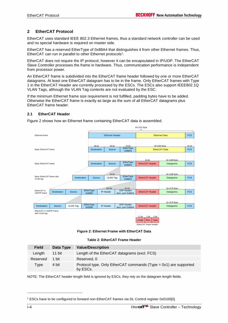
2 EtherCAT Protocol
EtherCAT uses standard IEEE 802.3 Ethernet frames, thus a standard network controller can be used and no special hardware is required on master side.
EtherCAT has a reserved EtherType of 0x88A4 that distinguishes it from other Ethernet frames. Thus, EtherCAT can run in parallel to other Ethernet protocols1.
EtherCAT does not require the IP protocol, however it can be encapsulated in IP/UDP. The EtherCAT Slave Controller processes the frame in hardware. Thus, communication performance is independent from processor power.
An EtherCAT frame is subdivided into the EtherCAT frame header followed by one or more EtherCAT datagrams. At least one EtherCAT datagram has to be in the frame. Only EtherCAT frames with Type 1 in the EtherCAT Header are currently processed by the ESCs. The ESCs also support IEEE802.1Q VLAN Tags, although the VLAN Tag contents are not evaluated by the ESC.
If the minimum Ethernet frame size requirement is not fulfilled, padding bytes have to be added. Otherwise the EtherCAT frame is exactly as large as the sum of all EtherCAT datagrams plus EtherCAT frame header.
2.1 EtherCAT Header
Figure 2 shows how an Ethernet frame containing EtherCAT data is assembled.
Ethernet Header
Destination SourceEtherType
0x88A4
Destination Source
Destination SourceEtherType
0x0800
Destination SourceEtherType
0x0800
IP HeaderUDP Header
dest. port 0x88A4
EtherType
0x88A4
Ethernet Data
EtherCAT Data
EtherCAT Header
FCS
FCS
FCS
FCS
FCSIP HeaderVLAN Tag
Datagrams
EtherCAT Header
EtherCAT Header
Length Res. Type
48 bit 48 bit 16 bit 32 bit
11 bit 1 bit 4 bit
160 bit 64 bit
32 bit
46-1500 Byte
16-1478 Byte
Datagrams
Datagrams
44-1498 Byte
16-1478 Byte
64-1522 Byte
UDP Header
dest. port 0x88A4
Destination SourceEtherType
0x88A4FCSEtherCAT Header Datagrams
16 bit 44-1498 Byte
Basic EtherCAT frame
EtherCAT in
UDP/IP frame
Basic EtherCAT frame with
VLAN tag
EtherCAT in UDP/IP frame
with VLAN tag
Basic EtherCAT frame
Ethernet frame
EtherCAT frame header
VLAN Tag
Figure 2: Ethernet Frame with EtherCAT Data
Table 2: EtherCAT Frame Header
Field Data Type Value/Description
Length 11 bit Length of the EtherCAT datagrams (excl. FCS)
Reserved 1 bit Reserved, 0
Type 4 bit Protocol type. Only EtherCAT commands (Type = 0x1) are supported by ESCs.
NOTE: The EtherCAT header length field is ignored by ESCs, they rely on the datagram length fields.
1 ESCs have to be configured to forward non-EtherCAT frames via DL Control register 0x0100[0].
EtherCAT Protocol
Slave Controller – Technology I-5
2.2 EtherCAT Datagram
Figure 3 shows the structure of an EtherCAT frame.
Datagram Header
FCS
FCS
Data
4 Byte
Position Addressing
1...n Datagrams
44*-1498 Byte
Ethernet header
Ethernet header
Length Res. Type
11 bit 1 bit 4 bit14 Byte
1st EtherCAT Datagram 2
nd ... n
th EtherCAT Datagram...
Working Counter
(WKC)
Cmd Idx
Position Offset
Address Offset
Logical Address
Address Len R C M IRQ
10 Byte 0-1486 Byte 2 Byte
8 Bit 8 Bit 32 Bit 11 Bit 16 Bit3 Bit 1 1
16 Bit 16 Bit
Node Addressing
Logical Addressing
* add 1-32 padding bytes if Ethernet frame is shorter than
64 Bytes (Ethernet Header+Ethernet Data+FCS)
Ethernet Data
EtherCAT header
168 6248 590 63 64 79
More EtherCAT Datagrams
Figure 3: EtherCAT Datagram

EtherCAT Protocol
I-6 Slave Controller – Technology
Table 3: EtherCAT Datagram
Field Data Type Value/Description
Cmd BYTE EtherCAT Command Type (see 2.5)
Idx BYTE The index is a numeric identifier used by the master for identification of duplicates/lost datagrams. It shall not be changed by EtherCAT slaves
Address BYTE[4] Address (Auto Increment, Configured Station Address, or Logical Address, see 2.3)
Len 11 bit Length of the following data within this datagram
R 3 bit Reserved, 0
C 1 bit Circulating frame (see 3.5):
0: Frame is not circulating
1: Frame has circulated once
M 1 bit More EtherCAT datagrams
0: Last EtherCAT datagram
1: More EtherCAT datagrams will follow
IRQ WORD EtherCAT Event Request registers of all slaves combined with a logical OR
Data BYTE[n] Read/Write Data
WKC WORD Working Counter (see 2.4)
2.3 EtherCAT Addressing Modes
Two addressing modes of EtherCAT devices are supported within one segment: device addressing and logical addressing. Three device addressing modes are available: auto increment addressing, configured station address, and broadcast. EtherCAT devices can have up to two configured station addresses, one is assigned by the master (Configured Station Address), the other one is stored in the SII EEPROM and can be changed by the slave application (Configured Station Alias address). The EEPROM setting for the Configured Station Alias address is only taken over at the first EEPROM loading after power-on or reset.
Table 4: EtherCAT Addressing Modes
Mode Field Data Type Value/Description
Auto Increment Address
Position WORD Each slave increments Position.
Slave is addressed if Position = 0.
Offset WORD Local register or memory address of the ESC
Configured Station Address
Address WORD Slave is addressed if Address matches Configured Station Address or Configured Station Alias (if enabled).
Offset WORD Local register or memory address of the ESC
Broadcast Position WORD Each slave increments Position (not used for addressing)
Offset WORD Local register or memory address of the ESC
Logical Address Address DWORD Logical Address (configured by FMMUs)
Slave is addressed if FMMU configuration matches Address.

EtherCAT Protocol
Slave Controller – Technology I-7
2.3.1 Device Addressing
The device can be addressed via Device Position Address (Auto Increment address), by Node Address (Configured Station Address/Configured Station Alias), or by a Broadcast.
Position Address / Auto Increment Address: The datagram holds the position address of the addressed slave as a negative value. Each slave increments the address. The slave which reads the address equal zero is addressed and will execute the appropriate command at receive. Position Addressing should only be used during start-up of the EtherCAT system to scan the fieldbus and later only occasionally to detect newly attached slaves. Using Position addressing is problematic if loops are closed temporarily due to hot connecting or link problems. Position addresses are shifted in this case, and e.g., a mapping of error register values to devices becomes impossible, thus the faulty link cannot be localized.
Node Address / Configured Station Address and Configured Station Alias: The configured Station Address is assigned by the master during start up and cannot be changed by the EtherCAT slave. The Configured Station Alias address is stored in the SII EEPROM and can be changed by the EtherCAT slave. The Configured Station Alias has to be enabled by the master. The appropriate command action will be executed if Node Address matches with either Configured Station Address or Configured Station Alias. Node addressing is typically used for register access to individual and already identified devices.
Broadcast: Each EtherCAT slave is addressed. Broadcast addressing is used e.g. for initialization of all slaves and for checking the status of all slaves if they are expected to be identical.
Each slave device has a 16 bit local address space (address range 0x0000:0x0FFF is dedicated for EtherCAT registers, address range 0x1000:0xFFFF is used as process memory) which is addressed via the Offset field of the EtherCAT datagram. The process memory address space is used for application communication (e.g. mailbox access).
2.3.2 Logical Addressing
All devices read from and write to the same logical 4 Gbyte address space (32 bit address field within the EtherCAT datagram). A slave uses a mapping unit (FMMU, Fieldbus Memory Management Unit) to map data from the logical process data image to its local address space. During start up the master configures the FMMUs of each slave. The slave knows which parts of the logical process data image have to be mapped to which local address space using the configuration information of the FMMUs.
Logical Addressing supports bit wise mapping. Logical Addressing is a powerful mechanism to reduce the overhead of process data communication, thus it is typically used for accessing process data.

EtherCAT Protocol
I-8 Slave Controller – Technology
2.4 Working Counter
Every EtherCAT datagram ends with a 16 Bit Working Counter (WKC). The Working Counter counts the number of devices that were successfully addressed by this EtherCAT datagram. Successfully means that the ESC is addressed and the addressed memory is accessible (e.g., protected SyncManager buffer). EtherCAT Slave Controllers increment the Working Counter in hardware. Each datagram should have an expected Working Counter value calculated by the master. The master can check the valid processing of EtherCAT datagrams by comparing the Working Counter with the expected value.
The Working Counter is increased if at least one byte/one bit of the whole multi-byte datagram was successfully read and/or written. For a multi-byte datagram, you cannot tell from the Working Counter value if all or only one byte was successfully read and/or written. This allows reading separated register areas using a single datagram by ignoring unused bytes.
The Read-Multiple-Write commands ARMW and FRMW are either treated like a read command or like a write command, depending on the address match.
Table 5: Working Counter Increment
Command Data Type Increment
Read command No success no change
Successful read +1
Write command No success no change
Successful write +1
ReadWrite command No success no change
Successful read +1
Successful write +2
Successful read and write +3

EtherCAT Protocol
Slave Controller – Technology I-9
2.5 EtherCAT Command Types
All supported EtherCAT Command types are listed in Table 6. For ReadWrite operations, the Read operation is performed before the Write operation.

EtherCAT Protocol
I-10 Slave Controller – Technology
Table 6: EtherCAT Command Types
CMD Abbr. Name Description
0 NOP No Operation Slave ignores command
1 APRD Auto Increment Read Slave increments address. Slave puts read data into the EtherCAT datagram if received address is zero.
2 APWR Auto Increment Write Slave increments address. Slave writes data into memory location if received address is zero.
3 APRW Auto Increment Read Write Slave increments address. Slave puts read data into the EtherCAT datagram and writes the data into the same memory location if received address is zero.
4 FPRD Configured Address Read Slave puts read data into the EtherCAT datagram if address matches with one of its configured addresses
5 FPWR Configured Address Write Slave writes data into memory location if address matches with one of its configured addresses
6 FPRW Configured Address Read Write
Slave puts read data into the EtherCAT datagram and writes data into the same memory location if address matches with one of its configured addresses
7 BRD Broadcast Read All slaves put logical OR of data of the memory area and data of the EtherCAT datagram into the EtherCAT datagram. All slaves increment position field.
8 BWR Broadcast Write All slaves write data into memory location. All slaves increment position field.
9 BRW Broadcast Read Write All slaves put logical OR of data of the memory area and data of the EtherCAT datagram into the EtherCAT datagram, and write data into memory location. BRW is typically not used. All slaves increment position field.
10 LRD Logical Memory Read Slave puts read data into the EtherCAT datagram if received address matches with one of the configured FMMU areas for reading.
11 LWR Logical Memory Write Slaves writes data to into memory location if received address matches with one of the configured FMMU areas for writing.
12 LRW Logical Memory Read Write Slave puts read data into the EtherCAT datagram if received address matches with one of the configured FMMU areas for reading. Slaves writes data to into memory location if received address matches with one of the configured FMMU areas for writing.
13 ARMW Auto Increment Read Multiple Write
Slave increments address. Slave puts read data into the EtherCAT datagram if received address is zero, otherwise slave writes the data into memory location.
14 FRMW Configured Read Multiple Write
Slave puts read data into the EtherCAT datagram if address matches with one of its configured addresses, otherwise slave writes the data into memory location.
15-255 reserved

EtherCAT Protocol
Slave Controller – Technology I-11
Table 7: EtherCAT Command Details
CMD High Addr. In
High Addr. Out
Low Addr.
Address Match Data
In
Data Out
WKC
NOP untouched none untouched
APRD Position Pos.+1 Offset ADP=0 - Read +0/1
APWR Position Pos.+1 Offset ADP=0 Write +0/1
APRW Position Pos.+1 Offset ADP=0 Write Read +0/1/2/3
FPRD Address Offset ADP=conf. station addr.
- Read +0/1
FPWR Address Offset ADP=conf. station addr.
Write +0/1
FPRW Address Offset ADP=conf. station addr.
Write Read +0/1/2/3
BRD High Add. In+1
Offset all Data In OR Read
+0/1
BWR High Add. In+1
Offset all Write +0/1
BRW High Add. In+1
Offset all Write Data In OR Read
+0/1/2/3
LRD Logical address FMMU - (Read AND bitmask1)
OR
(Data In AND NOT
bit_mask1)
+0/1
LWR Logical address FMMU Write +0/1
LRW Logical address FMMU Write (Read AND bit_mask1)
OR
(Data In AND NOT
bit_mask1)
+0/1/2/3
ARMW Position Pos.+1 Offset Read: ADP=0 - Read +0/1
Write: ADP/=0 Write +0/1
FRMW Address Offset Read: ADP= conf. station address./alias
- Read +0/1
Write: ADP/= conf. station address./alias
Write +0/1
NOTE: Working Counter (WKC) increment depends on address match
1 bit_mask depends on FMMU configuration if bit-wise mapping is used: only masked bits are actually addressed by the logical read/write command.

Frame Processing
I-12 Slave Controller – Technology
3 Frame Processing
The ET1100, ET1200, IP Core, and ESC20 slave controllers only support Direct Mode addressing: neither a MAC address nor an IP address is assigned to the ESC, they process EtherCAT frames with any MAC or IP address.
It is not possible to use unmanaged switches between these ESCs or between master and the first slave, because source and destination MAC addresses are not evaluated or exchanged by the ESCs. Only the source MAC address is modified when using the default settings, so outgoing and incoming frames can be distinguished by the master.
NOTE: Attaching an ESC directly to an office network will result in network flooding, since the ESC will reflect any frame – especially broadcast frames – back into the network (broadcast storm).
The frames are processed by the ESC on the fly, i.e., they are not stored inside the ESC. Data is read and written as the bits are passing the ESC. The forwarding delay is minimized to achieve fast cycle times. The forwarding delay is defined by the receive FIFO size and the EtherCAT Processing Unit delay. A transmit FIFO is omitted to reduce delay times.
The ESCs support EtherCAT, UDP/IP, and VLAN tags. EtherCAT frames and UDP/IP frames containing EtherCAT datagrams are processed. Frames with VLAN tags are processed by the ESCs, the VLAN settings are ignored and the VLAN tag is not modified.
The source MAC address is changed for every frame passing the EtherCAT Processing Unit (SOURCE_MAC[1] is set to 1 – locally administered address). This helps to distinguish between frames transmitted by the master and frames received by the master.
3.1 Loop Control and Loop State
Each port of an ESC can be in one of two states: open or closed. If a port is open, frames are transmitted to other ESCs at this port, and frames from other ESCs are received. A port which is closed will not exchange frames with other ESCs, instead, the frames are forwarded internally to the next logical port, until an open port is reached.
The loop state of each port can be controlled by the master (ESC DL Control register 0x0100). The ESCs supports four loop control settings, two manual configurations, and two automatic modes:
Manual open The port is open regardless of the link state. If there is no link, outgoing frames will be lost.
Manual close The port is closed regardless of the link state. No frames will be sent out or received at this port, even if there is a link with incoming frames.
Auto The loop state of each port is determined by the link state of the port. The loop is open if there is a link, and it is closed without a link.

Frame Processing
Slave Controller – Technology I-13
Auto close (manual open) The port is closed depending on the link state, i.e., if the link is lost, the loop will be closed (auto close). If the link is established, the loop will not be automatically opened, instead, it will remain closed (closed wait state). Typically, the port has to be opened by the master explicitly by writing the loop configuration again to the ESC DL Control register 0x0100. This write access has to enter the ESC via a different open port. There is an additional fallback option for opening the port: if a valid Ethernet frame is received at the closed port in Auto close mode, it will also be opened after the CRC is received correctly, without explicit master interaction.
open
closedclosed
wait
link lost
a) master writes loop
configuration again to AL Control
register (via another open port)
or
b) a valid Ethernet frame is
received at this port
link lost
link establishd
Figure 4: Auto close loop state transitions
A port is considered open if the port is available, i.e., it is enabled in the configuration, and one of the following conditions is met:
The loop setting in the DL Control register is Auto and there is an active link at the port.
The loop setting in the DL Control register is Auto close and there is an active link at the port and the DL Control register was written again after the link was established.
The loop setting in the DL Control register is Auto close and there is an active link at the port and a valid frame was received at this port after the link was established.
The loop setting in the DL control register is Always open
A port is considered closed if one of the following conditions is met:
The port is not available or not enabled in the configuration.
The loop setting in the DL Control register is Auto and there is no active link at the port.
The loop setting in the DL Control register is Auto close and there is no active link at the port or the DL Control register was not written again after the link was established
The loop setting in the DL Control register is Always closed
NOTE: If all ports are closed (either manually or automatically), port 0 will be opened as the recovery port. Reading and writing via this port is possible, although the DL status register reflects the correct status. This can be used to correct DL control register settings.
Registers used for loop control and loop/link status are listed in Table 8.
Table 8: Registers for Loop Control and Loop/Link Status
Register Address Name Description
0x0100[15:8] ESC DL Control Loop control/loop setting
0x0110[15:4] ESC DL Status Loop and link status
0x0518:0x051B PHY Port status PHY Management link status

Frame Processing
I-14 Slave Controller – Technology
3.2 Frame Processing Order
The frame processing order of EtherCAT Slave Controllers depends on the number of ports (logical port numbers are used):
Table 9: Frame Processing Order
Number of Ports Frame processing order
1 0→EtherCAT Processing Unit→0
2 0→EtherCAT Processing Unit→1 / 1→0
3 0→EtherCAT Processing Unit→1 / 1→2 / 2→0 (log. ports 0,1, and 2) or 0→EtherCAT Processing Unit→3 / 3→1 / 1→0 (log. ports 0,1, and 3)
4 0→EtherCAT Processing Unit→3 / 3→1 / 1→2 / 2→0
The direction through an ESC including the EtherCAT Processing Unit is called “processing” direction, other directions without passing the EtherCAT Processing Unit are called “forwarding” direction.
Ports which are not implemented behave similar to closed ports, the frame is forwarded to the next port.
Figure 5 shows the frame processing in general:
1
Port 2
Auto-
Forwarder
Port 1
Au
to-
Fo
rwa
rde
r
1
Port 3
Auto-
Forwarder
Port 0
Au
to-
Fo
rwa
rde
r
Loopback function
Lo
op
ba
ck fu
nctio
n
EtherCAT
Processing Unit
Loopback function
Lo
op
ba
ck fu
nctio
n
EtherCAT
Slave Controller
port 2 closed
port 2 open
po
rt 1
clo
se
d
po
rt 1
op
en
port 3 open
port 3 closed
po
rt 0
op
en
or
all
po
rts
clo
se
d
po
rt 0
clo
se
d
Figure 5: Frame Processing

Frame Processing
Slave Controller – Technology I-15
Example Port Configuration with Ports 0, 1, and 2
If there are only ports 0, 1, and 2, a frame received at port 0 goes via the Auto-Forwarder and the Loopback function to the EtherCAT Processing Unit which processes it. Then, the frame is sent to logical port 3 which is not configured, so the Loopback function of port 3 forwards it to port 1. If port 1 is closed, the frame is forwarded by the Loopback function to port 2. If port 1 is open, the frame is sent out at port 1. When the frame comes back into port 1, it is handled by the Auto-Forwarder and sent to port 2. Again, if port 2 is closed, the frame is forwarded to port 0, otherwise, it is sent out at port 2. When the frame comes back into port 2, it is handled by the Auto-Forwarder and then sent to the Loopback function of port 0. Then it is handled by the Loopback function and sent out at port 0 – back to the master.
3.3 Permanent Ports and Bridge Port
The EtherCAT ports of an ESC are typically permanent ports, which are directly available after Power-On. Permanent ports are initially configured for Auto mode, i.e., they are opened after the link is established. Additionally, some ESCs support an EtherCAT Bridge port (port 3), which is configured in the SII EEPROM like PDI interfaces. This Bridge port becomes available if the EEPROM is loaded successfully, and it is closed initially, i.e., it has to be opened (or set to Auto mode) explicitly by the EtherCAT master.
3.4 Shadow Buffer for Register Write Operations
The ESCs have shadow buffers for write operations to registers (0x0000 to 0x0F7F). During a frame, write data is stored in the shadow buffers. If the frame is received correctly, the values of the shadow buffers are transferred into the effective registers. Otherwise, the values of the shadow buffers are not taken over. As a consequence of this behavior, registers take their new value shortly after the FCS of an EtherCAT frame is received. SyncManagers also change the buffers after the frame was received correctly.
User and Process Memory do not have shadow buffers. Accesses to these areas are taking effect directly. If a SyncManager is configured to User Memory or Process Memory, write data will be placed in the memory, but the buffer will not change in case of an error.
3.5 Circulating Frames
The ESCs incorporate a mechanism for prevention of circulating frames. This mechanism is very important for proper watchdog functionality.
This is an example network with a link failure between slave 1 and slave 2:
EtherCAT
master
EtherCAT
slave 1Po
rt 0
Po
rt 1 EtherCAT
slave 2Po
rt 0
Po
rt 1 EtherCAT
slave 3Po
rt 0 EtherCAT
slave NPo
rt 0
Po
rt 0
Po
rt 1
Figure 6: Circulating Frames
Both slave 1 and slave 2 detect the link failure and close their ports (port 1 at slave 1 and port 0 at slave 2). A frame currently traveling through the ring at the right side of slave 2 might start circulating. If such a frame contains output data, it might trigger the built-in watchdog of the ESCs, so the watchdog never expires, although the EtherCAT master cannot update the outputs anymore.
To prevent this, a slave with no link at port 0 and loop control for port 0 set to Auto or Auto close (ESC DL Control register 0x0100) will do the following inside the EtherCAT Processing Unit:
If the Circulating bit of the EtherCAT datagram is 0, set the Circulating bit to 1
If the Circulating bit is 1, do not process the frame and destroy it
The result is that circulating frames are detected and destroyed. Since the ESCs do not store the frames for processing, a fragment of the frame will still circulate triggering the Link/Activity LEDs. Nevertheless, the fragment is not processed.

Frame Processing
I-16 Slave Controller – Technology
3.5.1 Unconnected Port 0
Port 0 must not be left intentionally unconnected (slave hardware or topology) because of the circulating frame prevention. All frames will be dropped after they have passed an automatically closed Port 0 for the second time, and this can prohibit any EtherCAT communication.
Example: Port 0 of slave 1 and 3 are automatically closed because nothing is connected. The Circulating bit of each frame is set at slave 3. Slave 1 detects this and destroys the frames.
EtherCAT
master
EtherCAT
slave 1Po
rt 0
Po
rt 1 EtherCAT
slave 2Po
rt 0
Po
rt 0
EtherCAT
slave 3Po
rt 0
Po
rt 1 EtherCAT
slave 4Po
rt 0
Po
rt 0
Port 3
Port 2
Port 3
Figure 7: All frames are dropped because of Circulating Frame Prevention
In redundancy operation, only one Port 0 is automatically closed, so the communication remains active.
3.6 Non-EtherCAT Protocols
If non-EtherCAT protocols are used, the forwarding rule in the ESC DL Control register (0x0100[0]) has to be set to forward non-EtherCAT protocols. Otherwise they are destroyed by the ESC.
3.7 Special Functions of Port 0
Port 0 of each EtherCAT is characterized by some special functions in contrast to ports 1, 2, and 3:
Port 0 leads to the master, i.e., port 0 is the upstream port, all other ports (1-3) are downstream ports (unless an error has occurred and the network is in redundancy mode).
The link state of Port 0 influences the Circulating Frame bit, and frames are dropped at port 0 if the bit is set and the link is automatically closed.
Port 0 loop state is open if all ports are closed (either automatically or manually).
Port 0 has a special behavior when using standard EBUS link detection.
Physical Layer Common Features
Slave Controller – Technology I-17
4 Physical Layer Common Features
EtherCAT supports two types of Physical Layers, Ethernet and EBUS. The Ethernet interface of ESCs is MII, RGMII, or RMII, connecting to an external Ethernet PHY according to IEEE 802.3 100BaseTX or FX. For EBUS, the physical layer is integrated into the EtherCAT ASICs. EtherCAT requires 100 Mbit/s links with full duplex communication.
The MII interface of Beckhoff ESCs is optimized e.g. for low processing/forwarding delay. The resulting additional requirements to Ethernet PHYs are described in the corresponding chapters.
4.1 Link Status
The link status of each port is available in the ESC DL Status register (0x0110:0x0111), most important are the “Communication established” bits 15, 13, 11, and 9. Additional link information is available in the PHY Port status register (0x0518:0x051B) if MI link detection and configuration is used. All other status bits are mainly for debugging purposes. The link status bits are described in the following table.
Table 10: Link Status Description
Status register
MII EBUS
LINK_MII signal Management Interface
Standard link detection
Enhanced link detection
Standard link detection
Enhanced link detection
Standard link detection
Enhanced link detection
ESC DL Status: Physical link 0x0110[7:4]
LINK_MII signal state LINK_MII signal combined with MI Link Detection and Configuration result
Result of the standard link detection mechanism
ESC DL Status: Communication established 0x0110[15,13,11,9]
LINK_MII signal state
LINK_MII signal state combined with RX_ERR threshold state
LINK_MII signal combined with MI Link Detection and Configuration result
LINK_MII signal combined with RX_ERR threshold state and MI Link Detection and Configuration result
Result of the standard link
detection mechanism.
Result of the enhanced link
detection mechanism.
PHY port status: physical link status 0x0518[0], 0x0519[0], 0x051A[0], 0x051B[0]
n.a.
PHY has detected link (PHY Status register 1[2])
n.a. PHY port status: Link status 0x0518[1], 0x0519[1], 0x051A[1], 0x051B[1]
PHY has detected link, link is suitable for ECAT
If all ports are closed (either manually or automatically, e.g., because no port has a communication link), port 0 is automatically opened as the recovery port. Reading and writing via this port is possible, although the DL status register reflects the correct status. This can be used to correct erroneous DL control register settings or to fix LINK_MII polarity configuration.

Physical Layer Common Features
I-18 Slave Controller – Technology
4.2 Selecting Standard/Enhanced Link Detection
Some ESCs distinguish between standard and enhanced link detection. Enhanced link detection provides additional security mechanisms regarding link establishment and surveillance. Using enhanced link detection is recommended for Ethernet PHY ports (refer to chapter 6.5 for compatibility issues with EBUS enhanced link detection). Some ESCs only support global Enhanced Link Detection configuration for all ports, some support port-wise configuration.
After power-on, enhanced link detection is enabled by default. It is disabled or remains enabled after the SII EEPROM is loaded according to the EEPROM setting (register 0x0141). An invalid EEPROM content will also disable enhanced link detection.
The EEPROM setting for enhanced Link detection is only taken over at the first EEPROM loading after power-on or reset. Changing the EEPROM and manually reloading it will not affect the enhanced link detection enable status (register 0x0110[2]), even if the EEPROM could not be read initially.
Registers used for Enhanced link detection are listed in Table 11.
Table 11: Registers for Enhanced Link Detection
Register Address Name Description
0x0141[1] ESC Configuration Enable/disable Enhanced link detection for all ports
0x0141[7:4] ESC Configuration Enable/disable Enhanced link detection port-wise
0x0110[2] ESC DL Status Enhanced link detection status
NOTE: Some of these register bits are set via SII EEPROM/IP Core configuration. Some of the registers are not available in specific ESCs. Refer to Section II and III for details.

Physical Layer Common Features
Slave Controller – Technology I-19
4.3 FIFO Size Reduction
The ESCs incorporate a receive FIFO (RX FIFO) for decoupling receive clock and processing clock. The FIFO size is programmable by the EtherCAT master (ESC DL Control register 0x0100). Some ESCs support a default value for the FIFO size loaded from the SII EEPROM.
The FIFO size values determine a reduction of the FIFO size, the FIFO cannot be disabled completely. The FIFO size can be reduced considering these three factors:
Accuracy of the receiver’s clock source
Accuracy of the sender’s clock source
Maximum frame size
The default FIFO size is sufficient for maximum Ethernet Frames and default Ethernet clock source accuracy (100 ppm). If the clock accuracy is 25 ppm or better, the FIFO size can be reduced to the minimum. If the FIFO size was accidentally reduced too much, a short 64 Byte frame should be sent for resetting the FIFO size to the default value, since a smaller frame is not utilizing the FIFO as much as a larger frame.
The FIFO size can be reduced to minimum if both sender and receiver have 25 ppm accuracy of their clock sources, even with maximum frame size.
Since 25 ppm clock accuracy can typically not be guaranteed for the entire life-time of a clock source, the actual clock deviation has to be measured on a regular basis for FIFO size reduction. If a slave does not support Distributed Clocks or the actual deviation is larger than 25 ppm, the FIFO size of all neighbors and the slave itself cannot be reduced. The actual deviation can be measured using Distributed Clocks:
Compare DC Receive Times over a period of time for slaves which only support DC Receive Times. Do not use this method if both slaves which are compared support DC Time Loop, since the measured deviation will approximate zero if the DC control loop has settled, but the actual deviation determining the FIFO size might be larger than 25 ppm.
Compare calculated deviation from register Speed Counter Diff (0x0932:0x0933) for adjacent slaves with DC Time Loop support after the DC control loop has settled (i.e., System Time Difference 0x092C:0x092F is at its minimum).
NOTE: Be careful with FIFO size reduction at the first slave if off-the-shelf network interface cards without 25 ppm accuracy are used by master.
Table 12: Registers for FIFO Size Reduction
Register Address Name Description
0x0100[18:16] ESC DL Control Current FIFO size setting
NOTE: Some of these register bits are set via SII EEPROM. Some of the registers are not available in specific ESCs. Refer to Section II and III for details.
4.4 Frame Error Detection
Refer to chapter 14 (Error Counters) for details on frame error detection.
Ethernet Physical Layer
I-20 Slave Controller – Technology
5 Ethernet Physical Layer
ESCs with Ethernet Physical Layer support use the MII interface, some do also support the RMII or RGMII interface. Since RMII/RGMII PHYs include FIFOs, they increase the forwarding delay of an EtherCAT slave device as well as the jitter. MII is recommended due to these reasons.
5.1 Requirements to Ethernet PHYs
EtherCAT and Beckhoff ESCs have some general requirements to Ethernet PHYs, which are typically fulfilled by state-of-the-art Ethernet PHYs.
The MII interfaces of Beckhoff ESCs are optimized for low processing/forwarding delays by omitting a transmit FIFO. To allow this, the Beckhoff ESCs have additional requirements to Ethernet PHYs, which are easily accomplished by several PHY vendors.
Refer to the EtherCAT Slave Controller application note “PHY Selection Guide” for Ethernet PHY requirements and example Ethernet PHYs.
Refer to Section III for ESC specific information about supported features.
5.2 PHY reset and Link partner notification/loop closing
The main principle of EtherCAT operation in case of link errors is disabling unreliable links by closing loops. This is automatically performed by the ESCs. The ESCs rely on the LINK_MII signal from the PHYs for detecting the link state.
It is crucial that a PHY does not establish a link while the ESC is not operating. Otherwise, the communication partner would also detect a physical link, causing him to open the communication link. Subsequently, all frames will get lost because the ESC is not operating.
So at least the following requirements have to be fulfilled, otherwise frames will be lost:
ESC in reset state → PHY disabled
The recommended solution for this issue is to enable the PHY together with the ESC by using the ESC’s reset signal for the PHY, too. If the ESC has individual PHY reset outputs, they should be used instead. This solution prevents the PHYs from establishing a link while the ESCs are not operating.

Ethernet Physical Layer
Slave Controller – Technology I-21
5.3 MII Interface
Refer to Section III for ESC specific MII information.
If an ESC MII interface is not used, LINK_MII has to be tied to a logic value which indicates no link, and RX_CLK, RXD, RX_ER, and especially RX_DV have to be tied to GND. The TX outputs can be left unconnected, unless they are used for ESC configuration.
Table 13: Special/Unused MII Interface signals
Signal Direction at PHY
Description
TX_CLK OUT ESC20: TX_CLK of one PHY is used as clock source, TX_CLK of other PHY is unused, leave open.
ESC dependent (e.g., IP Core):
TX_CLK is optionally used for automatic TX Shift compensation.
Other Beckhoff ESCs: Unused, leave unconnected.
COL OUT Collision detected.
ESC20: Connected, but not used.
Other Beckhoff ESCs: Unused. Leave unconnected.
CRS OUT Carrier sense.
ESC20: Connected, but not used.
Other Beckhoff ESCs: Unused. Leave unconnected
TX_ER IN Transmit error.
ESC20: Connected, always driven low.
Other Beckhoff ESCs: Connect to GND.
For more details about the MII interface, refer to IEEE Standard 802.3 (Clause 22), available from the IEEE.
Ethernet Physical Layer
I-22 Slave Controller – Technology
5.4 RMII Interface
Refer to Section III for ESC specific RMII information.
If an ESC RMII interface is not used, LINK_MII has to be tied to a logic value which indicates no link, and RXD, RX_ER, and especially CRS_DV have to be tied to GND. The TX signals can be left unconnected, unless they are used for ESC configuration.
For more details about the RMII interface, refer to the RMII Specification, available from the RMII consortium.
5.5 RGMII Interface
Refer to Section III for ESC specific RGMII information.
If an ESC RGMII interface is not used, LINK_MII has to be tied to a logic value which indicates no link, and RX_CLK, RX_CTL, and RXD have to be tied to GND. The TX signals can be left unconnected, unless they are used for ESC configuration.
For more details about the RGMII interface, refer to the “Reduced Gigabit Media Independent Interface (RGMII)” specification version 2.0.
5.5.1 RGMII In-Band Link Status
Some ESCs support RGMII PHYs. With these PHYs, it is possible to use the RGMII In-Band Status instead of the LINK_MII signal. In this case, the LINK_MII input of the ESC has to be tied to a value which indicates “no link”. The RGMII In-Band status is checked to indicate a 100 Mbit/s Full-Duplex link. The In-Band status is equivalent to the LINK_MII signal.
NOTE: Some PHYs require that RGMII In-Band Status is enabled by writing to the PHY management registers. This cannot be done by the ESC itself.
5.6 Link Detection
All ESCs support a LINK_MII signal for fast link detection at each Ethernet MII port. Some ESCs (e.g., EtherCAT IP Core) additionally support link detection and configuration via the MII management interface. Both the LINK_MII signals and the MI Link Detection and Configuration results (if available) are combined to determine the link state of each port, which is reflected in the ESC DL Status register (0x0110[15,13,11,9] – Communication established). Using the LINK_MII signal is mandatory since it is the only way to achieve fast link loss reaction times.
Table 14: Registers used for Ethernet Link Detection
Register Address Name Description
0x0110:0x0111 ESC DL Status Link Status (Link MII, Communication established)
0x0518:0x051B PHY Port Status MI Link Detection results if available
5.6.1 LINK_MII Signal
The LINK_MII signal used for link detection is typically an LED output signal of the Ethernet PHY. If available, LINK_MII should be connected to a combined signal indicating a 100 Mbit/s Full Duplex link. If such a signal is not available, a signal indicating a 100 Mbit/s link (speed LED) might be used. If only a Link signal is available (link LED), this might be used. Never use (combined) activity signals, e.g., Link/Act LED outputs, because the link state will toggle upon activity.
The main advantage of using a dedicated link signal instead of reading out MII management interface registers is the fast reaction time in case of a link loss. This is crucial for redundancy operation, since only one lost frame is tolerated. The EtherCAT port of an ESC which loses a link has to be closed as fast as possible to maintain EtherCAT communication at the other ports and to reduce the number of lost frames.
The LINK_MII signal state is reflected in the ESC DL Status register (0x0110[7:4]).

Ethernet Physical Layer
Slave Controller – Technology I-23
5.6.2 MI Link Detection and Configuration
The EtherCAT IP Core supports link detection and PHY configuration by using the MII management interface. Initially, the PHY configuration is checked and updated if necessary. Afterwards, the link status of each Ethernet port is cyclically polled. PHY accesses of the EtherCAT master are inferred upon request.
The MI Link Configuration mechanism configures the Ethernet PHYs to use Auto negotiation and advertise only 100BASE-TX Full-Duplex connections. Some ESCs support using Gigabit Ethernet PHYs, which are restricted to 100 Mbit/s links by the MI Link Configuration. ESCs which support FX operation natively are configuring the FX ports to use fixed 100BASE-TX Full-Duplex connections without Auto negotiation.
Depending on the physical layer configuration and the supported ESC features (e.g., TX vs. FX), the MI Link Detection will check if the link characteristics fulfill EtherCAT requirements (Auto negotiation, Speed, Duplex, etc.). If all conditions are met, an MI Link is detected.
Since the MI Link Detection does not solely rely on the PHY link status bit (register 1[2]), the local PHY and the remote PHY may indicate a link, but the ESC refuses it because it does not fulfill EtherCAT requirements. The current MI Link Detection state is reflected in the MI Interface registers (PHY Port Status 0x0518:0x051B).
MI Link Detection and Configuration must not be used without link detection via LINK_MII signals, because link loss reaction time would otherwise be to slow for redundancy operation. Enhanced Link Detection might not be a suitable solution in this case if too few RX_ERR are issued to the ESC before the PHY takes down the link.
NOTE: For testing it is possible to use MI Link Detection without LINK_MII signals: If the LINK_MII signals are statically set to “no link”, only MI Link Detection is used.
The MI Link Detection and Configuration checks the management communication with Ethernet PHYs. If communication is not possible – e.g. because no PHY is configured for the expected PHY address – the results are ignored. Take care of proper PHY address configuration to prevent erroneous behavior.
NOTE: Proper PHY address settings and PHY address offset configuration is crucial for MI Link Detection and Configuration.
5.7 Standard and Enhanced MII Link Detection
For Ethernet, the standard or enhanced MII link detection feature is a feature of link error detection and reaction. This has to be distinguished from the actual link detection, which tells the ESC if a physical link is available (i.e., the LINK_MII signal or the MI link detection and configuration mechanism).
Enhanced MII link detection, in contrast to standard MII link detection, will additionally disconnect a link if at least 32 RX errors (RX_ER) occur in a fixed interval of time (~10 µs). The local loop is closed and the link partner is informed by restarting the Auto-Negotiation mechanism via the MII Management Interface. This informs the link partner of the error condition, and the link partner will close the loop.
The ESC keeps the port closed until the link goes down during Auto-Negotiation and comes up again (the port remains closed if the link does not go down).
The availability of Enhanced MII Link Detection depends on a supported PHY address configuration, otherwise it has to be disabled.

Ethernet Physical Layer
I-24 Slave Controller – Technology
5.8 EtherCAT over Optical Links (FX)
EtherCAT communication over optical links using Ethernet PHYs is possible, but some requirements of EtherCAT have to be respected, and some characteristics of EtherCAT slave controllers have to be considered.
Some ESCs are prepared for FX operation, others require external logic to achieve EtherCAT compatibility.
Refer to the EtherCAT Slave Controller application note “PHY Selection Guide” for details on FX PHY connection and example schematics. The application note is available at the Beckhoff website (http://www.beckhoff.com).
5.8.1 Link partner notification and loop closing
The main principle of EtherCAT operation in case of link errors is disabling unreliable links by closing loops. This is automatically performed by the ESCs. The ESCs rely on the LINK_MII signal from the PHYs for detecting the link state.
With FX connections, it could happen that the Transceiver device is powered, while the PHY (and/or the ESC) is not active. The communication partner would detect a signal, causing him to open the link. All frames will get lost because the PHY (and/or the ESC) is not operating.
So at least the following two requirements have to be fulfilled, otherwise frames will be lost:
ESC in reset state → Transceiver disabled
PHY in reset state → Transceiver disabled
The recommended solution for this issue is to enable the transceiver together with the PHY by using the PHY’s reset signal for the transceiver, too. If the transceiver has no suitable input, the power supply of the transceiver can be switched off. Since the PHY’s reset should be controlled by the ESC’s reset output (either main reset output or individual PHY reset output), the transceiver will power down while the PHY is in the reset state and also while the ESC is in the reset state. Thus, the ESC and the PHY will be active when the transceiver gets active, and no frames are lost.
5.8.2 Far-End-Fault (FEF)
Some FX PHYs offer a Far-End-Fault (FEF) generation/detection feature. The intention is to inform the link partner of a bad link.
FEF Generation If an FEF-supporting PHY receives a signal with a quality which is not sufficient, the PHY will transmit a special FEF pattern to the link partner.
FEF Detection If an FEF-supporting PHY receives the FEF pattern with good signal quality, it will continue transmitting regularly, but it will indicate “no link” locally to the ESC, until the FEF pattern ends.
Conclusion The FEF feature is advantageous for EtherCAT, because the PHYs will only indicate a link when the signal quality is high enough. Without FEF, the EtherCAT slave controllers have to rely on the Enhanced Link detection feature for detecting a low quality link. Nevertheless, Enhanced Link detection becomes active only after the link is already established, thus, in case of a low quality link, the link status will be toggling on/off (link up → Enhanced link detection tears down link → link up …). This is sufficient to locate an issue in the network, but it might disturb operation of the remaining network.
So, it is highly recommended to use PHYs which fully implement FEF generation and detection.
NOTE: Some PHYs are claiming FEF support, but they are either not supporting FEF generation or detection, or they require configuration commands via MI management interface, which cannot be issued by the ESCs automatically.

Ethernet Physical Layer
Slave Controller – Technology I-25
5.8.3 ESCs with native FX support
ESCs with native FX support have individual PHY reset outputs for each port. This PHY reset output is intended to hold the PHY and the transceiver in reset state while the ESC is in reset state, and additionally, to issue a reset cycle when a link failure is detected by the enhanced link detection mechanism.
If at least one port is configured for FX operation, all ports have to use the individual PHY reset outputs. This is especially important for enhanced link detection, since all the PHY reset outputs are used for link down signaling instead of auto-negotiation restart, which is not used anymore – regardless of the port using FX or TX.
5.8.4 ESCs without native FX support
ESCs without native FX support require special attention regarding reset connection, link down signaling and enhanced link detection. External logic might be required.
5.9 Gigabit Ethernet PHYs
Gigabit Ethernet PHYs can generally be used for EtherCAT, as long as the link speed is restricted to 100 Mbit/s, either by strapping options of the PHY or by using the auto negotiation advertisement.
Some ESCs are capable of restricting the auto negotiation advertisement of Gigabit Ethernet PHYs to 100 Mbit/s full-duplex if MI link detection and configuration is enabled.
Nevertheless, all other requirements of EtherCAT have to be fulfilled – especially the link loss reaction time (Enhanced Link Detection might be required).
Ethernet Physical Layer
I-26 Slave Controller – Technology
5.10 MII Management Interface (MI)
Most EtherCAT slave controllers with MII/RMII/RGMII ports use the MII management interface for communication with the Ethernet PHYs. The MII management interface can be used by the EtherCAT master – or the local µController if supported by the ESC. Enhanced MII link detection uses the management interface for configuration and restarting auto negotiation after communication errors occurred (TX PHYs only). Some ESCs can make use of the MII management interface for link detection and PHY configuration. For fast link detection, the ESCs require to use a separate signal (LINK_MII).
Refer to chapter 5.6 for details about link detection with Ethernet PHYs. For more details about the MII management interface, refer to IEEE Standard 802.3 (Clause 22), available from the IEEE.
The ESCs support a shared MII Management Interface for all PHYs, i.e., MCLK and MDIO are connected to the ESC and to all PHYs.
5.10.1 PHY Addressing/PHY Address Offset
Proper PHY address configuration is crucial for Enhanced Link Detection and MI Link Detection and configuration, because the ESC itself needs to relate logical ports to the corresponding PHY addresses. The EtherCAT master can access the Ethernet PHYs using any address by means of the PHY address register 0x0513.
Typically, the logical port numbers match with the PHY addresses, i.e. the EtherCAT master and the ESC itself use PHY address 0 for accessing the PHY at port 0 (PHY address 1 for the PHY at port 1 and so on).
Depending on the ESC, there are two options for configuring the PHY addresses:
PHY address offset: The ESC accesses a PHY at logical port x with the address “x + PHY address offset”. Depending on the ESC only some or all possible offsets are configurable. The EtherCAT master uses the PHY addresses 0-3 to access the logical ports 0-3. These addresses are incremented by the PHY address offset inside the ESC. If the master uses PHY addresses 4-31, these addresses are also incremented by the PHY address offset inside the ESC.
Individual PHY address: The ESC accesses a PHY at each logical port with an individual PHY address. The EtherCAT master uses the PHY addresses 0-3 to access the logical ports 0-3. These addresses are replaced with the individual addresses inside the ESC. If the master uses PHY addresses 4-31, these addresses are not translated.
Depending on the ESC the PHY address configuration is a strapped at power-up, configured in advance (IP Core) or configured by signals.
Typically, the PHY address offset should be 0, and the logical port numbers match with the PHY addresses. Some Ethernet PHYs associate a special function with PHY address 0, e.g., address 0 is a broadcast PHY address. In these cases, PHY address 0 cannot be used. Instead, a PHY address offset different from 0 should be selected, preferably an offset which is supported by the ESC. If PHY addresses are chosen which are not supported by the ESC, Enhanced Link Detection and MI Link Detection and Configuration cannot be used and have to be disabled (the PHY address offset should be 0 in these cases). Nevertheless, the EtherCAT master can communicate with the PHYs using the actual PHY addresses, and EtherCAT communication is possible anyway – using the LINK_MII signal. It is recommended that the PHY addresses are selected to be equal to the logical port number plus 1 in this case. If port 0 is EBUS, ports 1-3 should have PHY addresses 1-3, i.e., PHY address offset is 0.
If the PHY address offset configuration of an ESC reflects the actual PHY address settings, the EtherCAT master can use addresses 0-3 in PHY address register 0x0513 for accessing the PHYs of logical ports 0-3, regardless of the PHY address offset.

Ethernet Physical Layer
Slave Controller – Technology I-27
Table 15: PHY Address configuration matches PHY address settings
Logical Port Configured address of the PHY PHY address register value used by EtherCAT master PHY address
offset = 0 PHY address
offset = 16
0 0 16 0
1 1 17 1
2 2 18 2
3 3 19 3
none 4-15 20-31 4-15
none 16-31 0-15 16-31
If the actual PHY address settings differ from the PHY address configuration of the ESC, the EtherCAT master has to use the actual PHY address mapping, i.e., PHY addresses 1-4 for accessing the PHYs of logical ports 0-3.
Table 16: PHY Address configuration does not match actual PHY address settings
Logical Port Configured address of the
PHY
PHY address register value used by EtherCAT master
0 1 1
1 2 2
2 3 3
3 4 4
none 0, 5-31 0, 5-13
NOTE: PHY address offset is 0 in this case (recommended).

Ethernet Physical Layer
I-28 Slave Controller – Technology
5.10.2 Logical Interface
The MI of the ESC is typically controlled by EtherCAT via the MI registers1.
Table 17: MII Management Interface Register Overview
Register Address Description
0x0510:0x0511 MII Management Control/Status
0x0512 PHY Address
0x0513 PHY Register Address
0x0514:0x0515 PHY Data
The MI supports two commands: write to one PHY register or read one PHY register.
5.10.2.1 MI read/write example
The following steps have to be performed for a PHY register access:
1. Check if the Busy bit of the MI Status register is cleared and the MI is not busy. 2. Write PHY address to PHY Address register. 3. Write PHY register number to be accessed into PHY Register Address register (0-31). 4. Write command only: put write data into PHY Data register (1 word/2 byte). 5. Issue command by writing to Control register.
For read commands, write 1 into Command Register Read 0x0510[8]. For write commands, write 1 into Write Enable bit 0x0510[0] and also 1 into Command Register Write 0x0510[9]. Both bits have to be written in one frame. The Write enable bit realizes a write protection mechanism. It is valid for subsequent MI commands issued in the same frame and self-clearing afterwards.
6. The command is executed after the EOF, if the EtherCAT frame had no errors. 7. Wait until the Busy bit of the MI Status register is cleared. 8. Check the Error bits of the MI Status register. The command error bit is cleared with a valid
command or by clearing the command register. The read error bit indicates a read error, e.g., a wrong PHY address. It is cleared by writing to the register.
9. Read command only: Read data is available in PHY Data register.
NOTE: The Command register bits are self-clearing. Manually clearing the command register will also clear the status information.
5.10.2.2 MI Interface Assignment to ECAT/PDI
The EtherCAT master controls the MI Interface (default) if the MII Management PDI Access State register 0x0517[0] is not set. The EtherCAT master can prevent PDI control over the MI Interface, and it can force the PDI to release the MI Interface control. After power-on, the PDI can take over MI Interface control without any master transactions.
1 ET1100 only: MI Control is transferred to PDI if the Transparent Mode is enabled. IP Core: MI Control by PDI is possible.

Ethernet Physical Layer
Slave Controller – Technology I-29
5.10.3 MI Protocol
Each MI access begins with a Preamble of “Ones“(32 without preamble suppression, less if both ESC and PHY support preamble suppression), followed by a Start-of-Frame (01) and the Operation Code (01 for write and 10 for read operations). Then the PHY address (5 bits) and the PHY register address (5 bits) are transmitted to the PHY. After a Turnaround (10 for write and Z0 for read operations – Z means MDIO is high impedance), two bytes of data follow. The transfer finishes after the second data byte and at least one IDLE cycle.
5.10.4 Timing specifications
Table 18: MII Management Interface timing characteristics
Parameter Comment
tClk MDC period
tWrite Write access time
tRead Read access time
1 0 1
1 0
0
MDC
MDIO
tClk
A4 A2A4 A1 R4A0 R3 R2
Preamble PHY Address
D7 D5D6 D4 D2D3 D1 D0
High Data Byte Low Data Byte
MDC
MDIO
tWrite
Start OP code
R1 R0
PHY Register Address
Turnaround
D15 D13D14 D12 D10D11 D9 D8
tWrite
IDLE
Figure 8: Write access
0
1 1 00
MDC
MDIO
tClk
A4 A2A4 A1 R4A0 R3 R2
Preamble PHY Address
D7 D5D6 D4 D2D3 D1 D0
High Data Byte Low Data Byte
MDC
MDIO
tRead
Start OP code
R1 R0
PHY Register Address
Turn-
around
D15 D13D14 D12 D10D11 D9 D8
tRead
IDLE
Figure 9: Read access

Ethernet Physical Layer
I-30 Slave Controller – Technology
5.11 MII management example schematic
The MII management interface is a shared bus for all PHYs. The example schematic shows the connection between ESC and PHYs. Take care of proper PHY address configuration.
ESC
Ethernet PHY
MDIO
MCLK
MDIO
MDC
4K
7
VCC I/O
Ethernet PHY
MDIO
MDC
Ethernet PHY
MDIO
MDC
Figure 10: MII management example schematic

Ethernet Physical Layer
Slave Controller – Technology I-31
5.12 Ethernet Termination and Grounding Recommendation
This termination and grounding design recommendation may help to meet the overall requirements for industrial communication. Nevertheless, implementation may vary depending on other requirements like board layout, other capacities, common ground interconnection, and shield grounding.
Unused RJ-45 pins are terminated by 75Ω resistors which will be connected to virtual ground. Virtual GND is connected to Protection Earth (PE) by a 10nF/500V capacitor in parallel to a 1MΩ resistor. Shield is also connected to PE by a 10nF/500V capacitor in parallel to a 1MΩ resistor. Especially the values for the connection between Virtual GND and PE are subject to change to meet industrial requirements (EMC). Shield is not directly connected with PE to avoid ground loops across large industrial plants with different PE potentials.
This design recommendation of termination and grounding is shown in Figure 11.
Protection
Earth (PE)
Virtual Ground
Protection
Earth (PE)
Magnetics
Shield
RJ-45
2
3
4
5
6
7
8
9
10
1
1 M
1 M
10
nF
/50
0 V
10 nF/500 V
> 2mm
gap
> 1mm gap between
PE and Virtual Ground
> 1mm
gap
plane connection
75
R
75
R
75
R
75
R
TX+
TX-
RX+
RX-
System
Ground
Figure 11: Termination and Grounding Recommendation
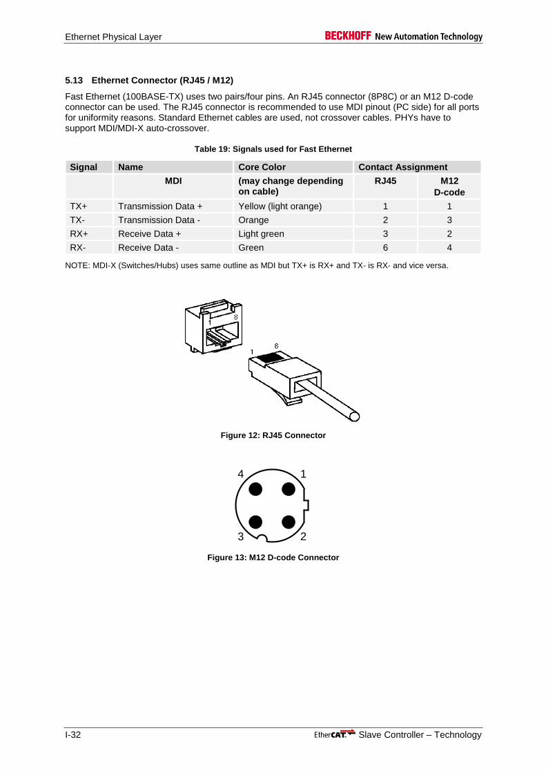
Ethernet Physical Layer
I-32 Slave Controller – Technology
5.13 Ethernet Connector (RJ45 / M12)
Fast Ethernet (100BASE-TX) uses two pairs/four pins. An RJ45 connector (8P8C) or an M12 D-code connector can be used. The RJ45 connector is recommended to use MDI pinout (PC side) for all ports for uniformity reasons. Standard Ethernet cables are used, not crossover cables. PHYs have to support MDI/MDI-X auto-crossover.
Table 19: Signals used for Fast Ethernet
Signal Name Core Color Contact Assignment
MDI (may change depending on cable)
RJ45 M12
D-code
TX+ Transmission Data + Yellow (light orange) 1 1
TX- Transmission Data - Orange 2 3
RX+ Receive Data + Light green 3 2
RX- Receive Data - Green 6 4
NOTE: MDI-X (Switches/Hubs) uses same outline as MDI but TX+ is RX+ and TX- is RX- and vice versa.
Figure 12: RJ45 Connector
3
4 1
2
Figure 13: M12 D-code Connector

Ethernet Physical Layer
Slave Controller – Technology I-33
5.14 Back-to-Back MII Connection
5.14.1 ESC to ESC Connection
Two EtherCAT slave controllers can be connected back-to-back using MII as shown in the figure below. The timing of RX_DV and RXD with respect to RX_CLK has to be checked at both ESCs to be compliant with the IEEE 802.3 requirements of min. 10 ns setup time and min. 10 ns hold time. The timing can be adjusted by configuring the TX Shift settings of each ESC.
Enhanced Link Detection cannot be enabled for the back-to-back ports on both ESCs.
Other clocking options besides using quartz oscillators are also possible. If CLK25_OUT is not available, REF_CLK can be used instead.
ESC
REF_CLK
LINK_MII*
RX_CLK
RX_DV
RXD[3:0]
TX_CLK
TX_EN
TXD[3:0]
RX_ER
MDC
MDIO
ESC
REF_CLK
RESET*
RX_CLK
RX_DV
RXD[3:0]
TX_CLK
TX_EN
TXD[3:0]
RX_ER
MDC
MDIO
25 MHz
4K
7
* check polarity: active Reset = no link
VCC I/O
4K
7
VCC I/O
Configure TX Shift and check RX timing (setup/hold>10 ns)
Configure TX Shift and check RX timing (setup/hold>10 ns)
CLK25_OUT
25 MHz
CLK25_OUT
LINK_MII*RESET*
Single clock source is possible, too.
Figure 14: Back-to-Back MII Connection (two ESCs)

Ethernet Physical Layer
I-34 Slave Controller – Technology
5.14.2 ESC to Standard Ethernet MAC
If an ESC is to be connected directly to a standard Ethernet MAC (e.g. µController or FPGA), RX timing at the ESC and the MAC has to be checked. Since TX Shift configuration is not possible in the MAC, RX_CLK for the ESC has to be adjusted (delayed) to achieve proper RX timing at the ESC.
An EtherCAT slave controller can be directly connected to a standard Ethernet MAC using MII as shown in the figure below. The timing of RX_DV and RXD with respect to RX_CLK has to be checked at both ESC and MAC to be compliant with the IEEE 802.3 requirements of min. 10 ns setup time and min. 10 ns hold time. The timing can be adjusted by configuring the TX Shift setting of the ESC and the clock buffer (e.g. using one or more buffers).
If the standard Ethernet MAC completely uses the IEEE 802.3 TX signal timing window of 0 to 25 ns, standard compliant RX timing (-10..10 ns) is impossible. Since most Beckhoff ESCs do not require the entire IEEE802.3 RX timing window (check in Section III), a valid configuration is possible even in this case.
ESC
REF_CLK
LINK_MII*
RX_CLK
RX_DV
RXD[3:0]
TX_CLK
TX_EN
TXD[3:0]
RX_ER
MDC
MDIO
Standard Ethernet
MAC (µC/FPGA)
CLK_IN
RX_CLK
RX_DV
RXD[3:0]
TX_CLK
TX_EN
TXD[3:0]
RX_ER
MDC
MDIO
25 MHz
4K
7
* if LINK_MII is act. low
VCC I/O
4K
7
VCC I/O
Configure TX Shift and
check RX timing
(setup/hold>10 ns)
Add delay (e.g.
clock buffers) to
adjust RX timing
(setup/hold>10 ns)
Figure 15: Back-to-Back MII Connection (ESC and standard MAC)

EBUS/LVDS Physical Layer
Slave Controller – Technology I-35
6 EBUS/LVDS Physical Layer
EBUS is an EtherCAT Physical Layer designed to reduce components and costs. It also reduces delay inside the ESC. The EBUS physical layer uses Low Voltage Differential Signaling (LVDS) according to the ANSI/TIA/EIA-644 “Electrical Characteristics of Low Voltage Differential Signaling (LVDS) Interface Circuits” standard.
EBUS has a data rate of 100 Mbit/s to accomplish the Fast Ethernet data rate. The EBUS protocol simply encapsulates Ethernet Frames, thus EBUS can carry any Ethernet frame – not only EtherCAT frames.
EBUS is intended to be used as a backplane bus, it is not qualified for wire connections.
6.1 Interface
Two LVDS signal pairs per EBUS link are used, one for reception and one for transmission of Ethernet/EtherCAT frames.
The EBUS interface has the following signals:
EtherCAT
device
EBUS-TX-
EBUS-TX+
EBUS-RX+
EBUS-RX-
RBIAS
Figure 16: EBUS Interface Signals
Table 20: EBUS Interface signals
Signal Direction Description
EBUS-TX+
EBUS-TX-
OUT EBUS/LVDS transmit signals
EBUS-RX+
EBUS-RX-
IN EBUS/LVDS receive signals
RBIAS BIAS resistor for EBUS-TX current adjustment
Unused EBUS ports can be left unconnected, only the LVDS termination resistor and the RBIAS resistor are mandatory.

EBUS/LVDS Physical Layer
I-36 Slave Controller – Technology
6.2 EBUS Protocol
Ethernet/EtherCAT frames are Manchester encoded (Biphase L) and encapsulated in Start-of-Frame (SOF) and End-of-Frame (EOF) identifiers. A beginning of a frame is detected if a Manchester violation with positive level (N+) followed by a ‘1’ bit occurs. The falling edge in the middle of the ‘1’ indicates the SOF to the ESC. This ‘1’ bit is also the first bit of the Ethernet preamble. Then the whole Ethernet frame is transmitted (including Ethernet SOF at the end of the preamble, up to the CRC). The frame finishes with a Manchester violation with negative level (N-), followed by a ‘0’ bit. This ‘0’ bit is also the first bit of the IDLE phase, which consists of ‘0’ bits.
EOF IDLE
tClk
Clock
Symbol
Manchester
Biphase L
IDLE
Data 0 0 N+ 1 0 1 0
Ethernet Preamble
1 N- 0 00/1
CRC
0/1
tSOF
tEOF
SOF
Figure 17: EBUS Protocol
6.3 Timing Characteristics
Table 21: EBUS timing characteristics
Parameter
Min Typ Max Comment
tClk 10 ns EBUS Clock (100 Mbit/s)
tSOF 15 ns Positive level of SOF before falling edge
tEOF 15 ns Negative level of EOF after last edge
NOTE: After power-on, a receiver which receives IDLE symbols cannot distinguish incoming ‘0’ bits from ‘1’ bits, because it is not synchronized to the transmitters phase. Synchronization is established at the falling edge at the end of the EBUS SOF, which indicates the center of the first preamble bit. After synchronization, idle errors can be detected by the ESC.
NOTE: SOF is detected at a falling edge following a period of at least 15 ns (nominal) of positive level, EOF is detected after a period of at least 15 ns (nominal) of negative level. I.e., the length of SOF and EOF can be even longer.

EBUS/LVDS Physical Layer
Slave Controller – Technology I-37
6.4 Standard EBUS Link Detection
Standard EBUS link detection is realized by counting the number of good signal events (no RX error) in a defined interval of time and comparing it to a given value. The link is established if enough events occurred, and disconnected if too few events occurred. IDLE symbols as well as any kind of EtherCAT traffic produce enough good events.
In order to handle partial link failures correctly, the following mechanism is used:
An ESC transmits at port 0 only if a link is detected (e.g., IDLE symbols are received), otherwise it will transmit N- symbols.
An ESC transmits at ports 1, 2, and 3 regardless of the link state (typically IDLE symbols if no frames are pending).
EtherCAT
master
EtherCAT
slave 1
Link A
Link B
Po
rt 0
Po
rt 1 EtherCAT
slave 2Po
rt 0
Po
rt 1
Figure 18: Example EtherCAT Network
This method addresses these two cases of partial link failure (see Figure 18):
A failure on Link A will be detected by Slave 2, which will stop transmitting anything on Link B (and close the loop at port 0). This is detected by Slave 1, which will close the loop at port 1. The master can still communicate with slave 1.
A failure on Link B will be detected by Slave 1, which will close the loop at port 1. The master can still communicate with slave 1. This failure cannot be detected by slave 2, which will leave port 0 open.
Do not connect any EBUS port 0 to another EBUS port 0 (same ESC or different ESCs) using standard link detection, because standard link detection will not establish a link after it was down.
Do not connect any EBUS port 1-3 to another EBUS port 1-3 (same ESC or different ESCs) using standard link detection, because partial link failures will not result in closed ports.
NOTE: Standard link detection cannot cope with a specific partial link fault (Link B failure), which affects redundancy operation (e.g., port 1 of slave 2 is connected to the master), because the master cannot communicate with slave 2 which leaves its port 0 open.
NOTE: Another advantage of this mechanism is that in case slave 2 is added to the network, at first port 0 of slave 2 is opened because there is activity on Link A, then transmission on Link B is started, and finally slave 1 opens Port 1. This assures that no frames get lost during link establishment.
6.5 Enhanced EBUS Link Detection
Enhanced EBUS link detection uses the standard link detection mechanism and adds a simple link detection handshake protocol before the link is established.
With enhanced link detection, the ESC transmits on all ports regardless of the link state (unless frames are transmitted; typically IDLE symbols are transmitted if no frames are pending).
The handshake protocol consists of three phases:
1. Each device starts transmitting a 4 nibble link request frame with 0x55C4 regularly at each port. This frame has no SOF/CRC and would be discarded if it was accidentally received by standard Ethernet devices (e.g., masters).
2. If a link request frame (0x55C4) is received at a port, the ESC will transmit link acknowledge frames (0x55CC) instead of link request frames at this port.
3. If a link acknowledge frame (0x55CC) is received at a port, the link at the port is established. Both link partners know that the link is good and establish the link. No further link detection frames are transmitted (until the link is interrupted and the link detection handshake phases are starting from the beginning).

EBUS/LVDS Physical Layer
I-38 Slave Controller – Technology
Link disconnection is signaled to the link partner by stopping transmission for a certain time. This will be detected by the default link detection mechanism. The link gets disconnected at both sides, and both sides close their loops. After that, the first phase of the handshake protocol starts again.
EBUS enhanced link detection is not compatible with older devices which forward enhanced link detection handshake frames depending on the direction (e.g. ESC20 and bus terminals without ASICs): the handshake frames are not forwarded through the EtherCAT Processing Unit, but they are forwarded without modification alongside the EtherCAT Processing Unit.
A device using enhanced link detection will stop generating handshake frames after the link is established or the enhanced link detection is disabled by SII EEPROM setting. It will restart generating handshake frames shortly after a link is lost (unless enhanced link detection is disabled).
6.6 EBUS RX Errors
The EBUS receiver detects the following RX errors:
Missing edge in the middle of one bit (but not EBUS SOF/EOF)
EBUS SOF inside a frame (two SOFs without EOF in between)
EBUS EOF outside a frame (two EOFs without SOF in between)
IDLE violation: ‘1’ outside a frame
Too short pulses (less than ~3.5 ns)
A frame with an RX error is discarded. Too many RX errors in a defined interval of time will result in link disconnection.
Errors outside of a frame are counted only once, and errors inside a frame are also counted only once, because the Manchester decoding might have lost synchronization.
6.7 EBUS Low Jitter
In Low Jitter mode, the jitter of the forwarding delay (EBUS port to EBUS port) is reduced.
6.8 EBUS Connection
The connection of two EBUS ports is shown in Figure 19. LVDS termination with 100 Ohm impedance is necessary between each pair of receive signals – located adjacent to the receive inputs.
EtherCAT
device
TX+
TX-
RX+
RX-
10
0R
10
0R
EtherCAT
device
RX+
RX-
TX+
TX-
Figure 19: EBUS Connection

FMMU
Slave Controller – Technology I-39
7 FMMU
Fieldbus Memory Management Units (FMMU) convert logical addresses into physical addresses by the means of internal address mapping. Thus, FMMUs allow to use logical addressing for data segments that span several slave devices: one datagram addresses data within several arbitrarily distributed ESCs. Each FMMU channel maps one continuous logical address space to one continuous physical address space of the slave. The FMMUs of Beckhoff ESCs support bit wise mapping, the number of supported FMMUs depends on the ESC. The access type supported by an FMMU is configurable to be either read, write, or read/write.
Figure 20: FMMU Mapping Principle
The following example illustrates the functions of an FMMU configured to map 14 bits from logical address 0x00010011.3 to 0x00010013[0] to the physical register bits 0x0F01[1] to 0x0F02[6]. The FMMU length is 3 Byte, since the mapped bits span 3 Bytes of the logical address space. Length calculation begins with the first logical byte which contains mapped bits, and ends with the last logical byte which contains mapped bits.
Table 22: Example FMMU Configuration
FMMU configuration register FMMU reg. offset Value
Logical Start Address 0x0:0x3 0x00010011
Length (Bytes) 0x4:0x5 3
Logical Start bit 0x6 3
Logical Stop bit 0x7 0
Physical Start Address 0x8:0x9 0x0F01
Physical Start bit 0xA 1
Type 0xB read and/or write
Activate 0xC 1 (enabled)
NOTE: FMMU configuration registers start at address 0x0600.
Log
ica
l pro
cess im
age: up
to 4
GB
yte
0
232Telegram structure
Ethernet HDR HDR 1 PLC Data HDR 2 NC Data HDR n Data n FCS
PLC Data
Data n
NC Data
DVI
IPC
..
..
Sub-
Telegram 1Sub-
Telegram 2
Sub-
Telegram n

FMMU
I-40 Slave Controller – Technology
0 7654321 0 7654321 0 7654321 076
Byte 0x00010011
Logical Start Address
1
0 7654321 0 7654321 0 7654321 076 1
Byte 0x00010012 Byte 0x00010013
Byte 0x0F02Byte 0x0F02Byte 0x0F01
Physical Start Address
Logical Address Space
Physical Address Space
Logical Start bit = 3 Logical Stop Bit = 0
Physical Start bit = 1
Configured FMMU Length = 3 Bytes
14 Bits mapped
Figure 21: FMMU Mapping Example
Attention: This drawing of the bit string shows the least significant bit first, in a hexadecimal representation of the octets the least significant value is at the right place and the most significant on the left place (00110011 is represented as octet by 0xCC).
Restrictions on FMMU Settings
The FMMUs of Beckhoff ESCs are subject to restrictions. The logical address ranges of two FMMUs of the same direction (read or write) in one ESC must be separated by at least 3 logical bytes not configured by any FMMU of the same type, if one of the FMMUs or both use bit-wise mapping (logical start bit ≠ 0, logical stop bit ≠ 7, or physical start bit ≠ 0). In the above example, the first logical address area after the one shown must have a logical start address of 0x00010017 or higher (the last byte of the example FMMU is 0x00010013, three bytes free 0x00010014-0x00010016).
If only byte-wise mapping is used (logical start bit = 0, logical stop bit = 7, or physical start bit = 0), the logical address ranges can be adjacent.
Bit-wise writing is only supported by the Digital Output register (0x0F00:0x0F03). All other registers and memories are always written byte-wise. If bit-wise mapping is used for writing into these areas, bits without mapping to logical addresses are written with undefined values (e.g., if only physical address bit 0x1000[0] is mapped by a write FMMU, the bits 1-7 are written with undefined values).
Additional FMMU Characteristics
Each logical address byte can at most be mapped either by one FMMU(read) plus one FMMU(write), or by one FMMU(read/write). If two or more FMMUs (with the same direction – read or write) are configured for the same logical byte, the FMMU with the lower number (lower configuration address space) is used, the other ones are ignored.
One or more FMMUs may point to the same physical memory, all of them are used. Collisions cannot occur.
It is the same to use one read/write FMMU or two FMMUs – one read, the other one write – for the same logical address.
A read/write FMMU cannot be used together with SyncManagers, since independent read and write SyncManagers cannot be configured to use the same (or overlapping) physical address range.
Bit-wise reading is supported at any address. Bits which are not mapped to logical addresses are not changed in the EtherCAT datagram. E.g., this allows for mapping bits from several ESCs into the same logical byte.
Reading an unconfigured logical address space will not change the data.
SyncManager
Slave Controller – Technology I-41
8 SyncManager
The memory of an ESC can be used for exchanging data between the EtherCAT master and a local application (on a µController attached to the PDI) without any restrictions. Using the memory for communication like this has some drawbacks which are addressed by the SyncManagers inside the ESCs:
Data consistency is not guaranteed. Semaphores have to be implemented in software for exchanging data in a coordinated way.
Data security is not guaranteed. Security mechanisms have to be implemented in software.
Both EtherCAT master and application have to poll the memory in order to find out when the access of the other side has finished.
SyncManagers enable consistent and secure data exchange between the EtherCAT master and the local application, and they generate interrupts to inform both sides of changes.
SyncManagers are configured by the EtherCAT master. The communication direction is configurable, as well as the communication mode (Buffered Mode and Mailbox Mode). SyncManagers use a buffer located in the memory area for exchanging data. Access to this buffer is controlled by the hardware of the SyncManagers.
A buffer has to be accessed beginning with the start address, otherwise the access is denied. After accessing the start address, the whole buffer can be accessed, even the start address again, either as a whole or in several strokes. A buffer access finishes by accessing the end address, the buffer state changes afterwards and an interrupt or a watchdog trigger pulse is generated (if configured). The end address cannot be accessed twice inside a frame.
Two communication modes are supported by SyncManagers:
Buffered Mode - The buffered mode allows both sides, EtherCAT master and local application, to access the
communication buffer at any time. The consumer always gets the latest consistent buffer which was written by the producer, and the producer can always update the content of the buffer. If the buffer is written faster than it is read out, old data will be dropped.
- The buffered mode is typically used for cyclic process data.
Mailbox Mode - The mailbox mode implements a handshake mechanism for data exchange, so that no data will
be lost. Each side, EtherCAT master or local application, will get access to the buffer only after the other side has finished its access. At first, the producer writes to the buffer. Then, the buffer is locked for writing until the consumer has read it out. Afterwards, the producer has write access again, while the buffer is locked for the consumer.
- The mailbox mode is typically used for application layer protocols.
The SyncManagers accept buffer changes caused by the master only if the FCS of the frame is correct, thus, buffer changes take effect shortly after the end of the frame.
The configuration registers for SyncManagers are located beginning at register address 0x0800.
Table 23: SyncManager Register overview
Description Register Address Offset
Physical Start Address 0x0:0x1
Length 0x2:0x3
Control Register 0x4
Status Register 0x5
Activate 0x6
PDI Control 0x7

SyncManager
I-42 Slave Controller – Technology
8.1 Buffered Mode
The buffered mode allows writing and reading data simultaneously without interference. If the buffer is written faster than it is read out, old data will be dropped. The buffered mode is also known as 3-buffer-mode.
Physically, 3 buffers of identical size are used for buffered mode. The start address and size of the first buffer is configured in the SyncManager configuration. The addresses of this buffer have to be used by the master and the local application for reading/writing the data. Depending on the SyncManager state, accesses to the first buffer’s (0) address range are redirected to one of the 3 buffers. The memory used for buffers 1 and 2 cannot be used and should be taken into account for configuring other SyncManagers.
One buffer of the three buffers is allocated to the producer (for writing), one buffer to the consumer (for reading), and the third buffer keeps the last consistently written data of the producer.
As an example, Figure 22 demonstrates a configuration with start address 0x1000 and Length 0x100. The other buffers shall not be read or written. Access to the buffer is always directed to addresses in the range of buffer 0.
0x1000 - 0x10FF
Buffer 0 (visible)
All buffers are controlled by the SyncManager. Only buffer 0 is configured by the SyncManager and addressed by ECAT and µController.
0x1100 - 0x11FF
Buffer 1 (invisible shall not be used)
0x1200 - 0x12FF
Buffer 2 (invisible shall not be used)
0x1300 … Next usable RAM space
Figure 22: SyncManager Buffer allocation
The buffer interaction is shown in Figure 23:
Master ECAT NEXT PDI µController
Write begin Load next buffer if new data available
Read begin
Write end
Exchange buffer (if frame is ok)
Read end
Exchange buffer
Write begin Write end
Read begin
Read end
Load next buffer if new data available
Figure 23: SyncManager Buffered Mode Interaction

SyncManager
Slave Controller – Technology I-43
The Status register of the SyncManager reflects the current state. The last written buffer is indicated (informative only, access redirection is performed by the ESC), as well as the interrupt states. If the SyncManager buffer was not written before, the last written buffer is indicated to be 3 (start/empty).
8.2 Mailbox Mode
The mailbox mode only allows alternating reading and writing. This assures all data from the producer reaches the consumer. The mailbox mode uses just one buffer of the configured size.
At first, after initialization/activation, the buffer (mailbox, MBX) is writeable. Once it is written completely, write access is blocked, and the buffer can be read out by the other side. After it was completely read out, it can be written again.
The time it takes to read or write the mailbox does not matter.
Master µController
Write Mailbox
Write
Write w. failure (Mailbox full)
Mailbox full Mailbox empty
Read Read w. failure (Mailbox empty)
Read Mailbox
Read
Read w. failure (Mailbox empty)
Mailbox full Mailbox empty
Write Write w. failure (Mailbox full)
Figure 24: SyncManager Mailbox Interaction
8.2.1 Mailbox Communication Protocols
This is only a brief overview of the mailbox communication protocols. For details on the mailbox protocols refer to the EtherCAT specification ETG.1000.6: “Application layer protocol specification” available from the EtherCAT Technology Group (http://www.ethercat.org) or to the IEC specification “Digital data communications for measurement and control – Fieldbus for use in industrial control systems”, IEC 61158 Type 12: EtherCAT, available from the IEC (http://www.iec.ch).
Ethernet over EtherCAT (EoE) Defines a standard way to exchange or tunnel standard Ethernet Frames over EtherCAT.
CAN application layer over EtherCAT (CoE) Defines a standard way to access a CAN application layer object dictionary and to exchange CAN application layer Emergency and PDO messages on an event driven path.
File Access over EtherCAT (FoE) Defines a standard way to download and upload firmware and other ‘files’.
Servo Profile over EtherCAT (SoE) Defines a standard way to access the IEC 61800-7 identifier.
Vendor specific Profile over EtherCAT (VoE) A vendor specific protocol follows after a VoE header that identifies the vendor and a vendor specific type.
ADS over EtherCAT (AoE) AoE defines a standard way to exchange Automation Device Specification (ADS) messages over EtherCAT.

SyncManager
I-44 Slave Controller – Technology
The content of an EtherCAT mailbox header is shown in Figure 25.
Figure 25: EtherCAT Mailbox Header (for all Types)
Table 24: EtherCAT Mailbox Header
Field Data Type Value/Description
Length WORD Number of Bytes of this mailbox command excluding the mailbox header
Address WORD Station Address of originator
Channel 6 bit 0 – reserved for future use
Priority 2 bit Priority between 0 (lowest) and 3 (highest)
Type 4 bit Mailbox protocol types:
0x0: Error
0x1: Vendor specific (Beckhoff: AoE – ADS over EtherCAT)
0x2: EoE (Ethernet over EtherCAT)
0x3: CoE (CAN application layer over EtherCAT)
0x4: FoE (File access over EtherCAT)
0x5: SoE (Servo profile over EtherCAT)
0xF: Vendor specific (VoE)
Ctr. 3 bit Sequence number that is used for detection of duplicated frames
Reserved 1 bit 0
8.3 PDI register function acknowledge by Write
Refer to chapter 16.2 for the background of this function, which only affects the SyncManager operation when the PDI reads a buffer. The EtherCAT operation is not influenced by this optional feature.
Reading a SyncManager buffer consists of the following steps, if PDI register function acknowledge by Write is enabled:
Read the first byte. This will open the buffer. Accidentally reading subsequent bytes has no influence.
Read any byte of the buffer. This includes the first byte, the last byte, and any inner byte. The buffer remains open, and the buffer can even be read multiple times. Accidentally reading the last byte has no influence.
Write to the last byte of the buffer. Byte enable signals are used, write data is ignored (write 0). This write operation closes the buffer.
Accidentally reading the first byte of a second SyncManager buffer behind the one to be read is still possible, this will open the second SyncManager buffer. This can easily be prevented by aligning SyncManager buffer start addresses to the data width of the µController. It is recommended to align SyncManager buffer start addresses to 64 bit (8 byte) boundaries anyway.
8.4 Interrupt and Watchdog Trigger Generation, Latch Event Generation
Interrupts can be generated when a buffer was completely and successfully written or read. A watchdog trigger signal can be generated to rewind (trigger) the Process Data watchdog used for Digital I/O after a buffer was completely and successfully written. Interrupt and watchdog trigger generation are configurable. The SyncManager Status register reflects the current buffer state.
For debugging purposes it is also possible to trigger Distributed Clock Latch events upon successful buffer accesses (for some ESCs).
Ctr. Type Prio Channel Address Length
16 Bit 16 Bit 6 Bit 2 Bit 4 Bit 3 Bit 1 Bit
0 16 32 38 40 44 0.
47

SyncManager
Slave Controller – Technology I-45
8.5 Single Byte Buffer Length / Watchdog Trigger for Digital Output PDI
If a SyncManager is configured for a length of 1 byte (or even 0), the buffer mechanism is disabled, i.e., read/write accesses to the configured address will pass the SyncManager without interference. The additional buffers 1 and 2 are not used in buffered mode, and alternation of write/read accesses is not necessary for mailbox mode. Consistency is not an issue for a single byte buffer.
Nevertheless, watchdog generation is still possible if the buffer length is 1 byte (interrupt generation as well).
NOTE: For some ESCs in Mailbox mode, watchdog and interrupt generation are depending on the alternation of write and read accesses, although the write/read accesses itself are executed without interference. I.e., Buffered mode should be used for single byte buffers for watchdog generation.
Watchdog trigger generation with single byte SyncManagers is used for Digital Outputs, because the outputs are only driven with output data if the Process Data watchdog is triggered. One SyncManager has to be configured for each byte of the Digital Output register (0x0F00:0x0F03) which is used for outputs. The SyncManagers have to be configured like this:
Buffered Mode (otherwise the process data watchdog will not be wound up with some ESCs upon the second and following writes, because the Digital I/O PDI does not read the addresses)
Length of 1 byte
EtherCAT write / PDI read
Watchdog Trigger enabled
For more details refer to the Digital I/O PDI description of Section III and the chapters about Watchdog and Digital Output in this document.
NOTE: A SyncManager with length 0 behaves like a disabled SyncManager. It does not interfere accesses nor generate interrupt or watchdog trigger signals.
8.6 Repeating Mailbox Communication
A lost datagram with mailbox data is handled by the application layer. The Repeat Request/Repeat Acknowledge bits in the SyncManager Activation register (offset 0x06[1]) and the PDI Control register (offset 0x07[1]) are used in mailbox mode for retransmissions of buffers from a slave to the master. If a mailbox read frame gets lost/broken on the way back to the master, the master can toggle the Repeat Request bit. The slave polls this bit or receives an interrupt (SyncManager activation register changed, register 0x0220[4]) and writes the last buffer again to the SyncManager. Then the PDI toggles the Repeat Acknowledge bit in the PDI Control register. The master will read out this bit and read the buffer content. Communication resumes afterwards.
This mechanism is shown in Figure 26 for a mailbox write service. The Mailbox confirmation is lost on its way from the slave to the master and has to be repeated again.

SyncManager
I-46 Slave Controller – Technology
Master µController
Slave writes data into mailbox
Master sends mailbox read
command
Mailbox read
Slave detects Repeat Request
(interrupt or polling)
Slave writes stored write data
into mailbox again
Maibox read data (WKC=1)
Timeout: Master detects
lost frame
Master toggles
Repeat Request bit
Toggle Repeat Request bit
Master polls Repeat Request
Acknowledge bit
Read Repeat Request Acknowledge bit
Repeat Request Acknowledge is set
Master sends mailbox read
command again
Mailbox read
Maibox read data A (WKC=1)Master receives mailbox read
data
ESC
Write data A
Interrupt
Write data A
Toggle Repeat
Request
Acknowledge
Read Event
Slave detects that mailbox was
read and stores write data for a
possible repeat request
Write data B Slave writes next data into
mailbox
Slave toggles Repeat Request
Acknowledge bit
Communication proceeds with read data B
Figure 26: Handling of a Repeat Request with Read Mailbox
8.7 SyncManager Deactivation by the PDI
A SyncManager can be deactivated by the PDI to inform the master of local problems (typically used in buffered mode only). The master can detect SyncManager deactivation by checking the Working Counter, which is not incremented if a deactivated SyncManager buffer is accessed. If a SyncManager is deactivated by the PDI (PDI Control register 0x7[0]=1), the state of the SyncManager is reset, interrupts are cleared and the SyncManager has to be written first after re-activation. The entire SyncManager buffer area is read/write protected while the SyncManager is deactivated by the PDI.

Distributed Clocks
Slave Controller – Technology I-47
9 Distributed Clocks
The Distributed Clocks (DC) unit of EtherCAT slave controllers supports the following features:
Clock synchronization between the slaves (and the master)
Generation of synchronous output signals (SyncSignals)
Precise time stamping of input events (LatchSignals)
Generation of synchronous interrupts
Synchronous Digital Output updates
Synchronous Digital Input sampling
9.1 Clock Synchronization
DC clock synchronization enables all EtherCAT devices (master and slaves) to share the same EtherCAT System Time. The EtherCAT devices can be synchronized to each other, and consequently, the local applications are synchronized as well.
For system synchronization all slaves are synchronized to one Reference Clock. Typically, the first ESC with Distributed Clocks capability after the master within one segment holds the reference time (System Time). This System Time is used as the reference clock to synchronize the DC slave clocks of other devices and of the master. The propagation delays, local clock sources drift, and local clock offsets are taken into account for the clock synchronization.
The ESCs can generate SyncSignals for local applications to be synchronized to the EtherCAT System Time. SyncSignals can be used directly (e.g., as interrupts) or for Digital Output updating/Digital Input sampling. Additionally, LatchSignals can be time stamped with respect to the EtherCAT System Time.
Definition of the System Time
Beginning on January, 1st 2000 at 0:00h
Base unit is 1 ns
64 bit value (enough for more than 500 years)
Lower 32 bits span over 4.2 seconds (typically enough for communication and time stamping). Some ESCs only have 32 bit DCs, which are compatible with 64 bit DCs.
Definition of the Reference Clock One EtherCAT device will be used as a Reference Clock. Typically, the Reference Clock is the first ESC with DC capability between master and all the slaves to be synchronized (DC slaves). The Reference Clock might be adjusted to a “global” reference clock, e.g. to an IEEE 1588 grandmaster clock. The reference clock provides the System Time.
Definition of the Local Clock Each DC slave has a local clock, initially running independent of the Reference Clock. The difference between local clock and Reference Clock (offset) can be compensated, as well as clock drifts. The offset is compensated by adding it to the local clock value. The drift is compensated by measuring and adjusting the local clock speed.
Each DC slave holds a copy of the Reference Clock, which is calculated from the local clock and the local offset. The Reference Clock has a local clock, too.
Definition of the Master Clock The Reference Clock is typically initialized by the EtherCAT master using the master clock to deliver the System Time according to the System Time definition. The EtherCAT master clock is typically bound to a global clock reference (RTC or the master PC, IEEE1588, GPS, etc.), which is either directly available to the master or indirectly by an EtherCAT slave providing access to the reference.

Distributed Clocks
I-48 Slave Controller – Technology
Propagation Delay The propagation delay between Reference Clock and slave clock has to be taken into account when the System Time is distributed to the slaves.
Offset The offset between local clock and Reference Clock has two reasons: the propagation delay from the ESC holding the Reference Clock to the device with the slave clock, and initial differences of the local times resulting from different times at which the ESCs have been powered up. This offset is compensated locally in each slave.
The ESC holding the Reference Clock derives the System Time from its local time by adding a local offset. This offset represents the difference between local time (started at power-up) and master time (starting on January, 1st 2000 at 0:00h).
Drift Since Reference Clock and DC slaves are typically not sourced by the same clock source (e.g., a quartz), their clock sources are subject to small deviations of the clock periods. The result is that one clock is running slightly faster than the other one, their local clocks are drifting apart.
ESC Classification regarding DC Support Three classes of ESCs are distinguished regarding Distributed Clocks support: 1. Slaves supporting System Time/Time Loop Control Unit:
Receive time stamps and System Time/Time Loop Control Unit available; SyncSignal generation, LatchSignal time stamping, and SyncManager Event Times are optionally supported depending on application.
2. Slaves supporting only propagation delay measurement: Mandatory for ESCs with 3 or more ports (topology devices like EK1100 and ET1100). Local clock and receive time stamps are supported.
3. Slaves without Distributed Clocks support: Slaves with max. 2 ports do not have to support DC features. Processing/forwarding delay of such slaves is treated like a “wire delay” by the surrounding DC capable slaves.

Distributed Clocks
Slave Controller – Technology I-49
9.1.1 Clock Synchronization Process
The clock synchronization process consists of three steps:
1. Propagation Delay Measurement: The master initiates propagation delay measurement between all slaves in all directions. Each EtherCAT slave controller measures the receive time of the measurement frame. The master collects the time stamps afterwards and calculates the propagation delays between all slaves.
2. Offset compensation to Reference Clock (System Time): The local time of each slave clock is compared to the System Time. The difference is compensated individually by writing it to each slave. All devices get the same absolute System Time.
3. Resetting the Time Control Loop: The current filter status needs to be reset to eliminate influences of previous measurements and improve repeatability.
4. Drift compensation to Reference Clock: The drift between Reference Clock and local clock has to be compensated by regularly measuring the differences and readjusting the local clocks.
The following figure illustrates the compensation calculations for two cases, in the first case the System Time is less than the slave’s local time, in the second case, it is the other way around.
Reference
Clock
Slave Clock
tSystem Time tLocal time
Drift compensation fra
me
carrying current System Time
TX
Propagation delay compensation
Offset compensation
Drift compensation
Reference
Clock
Slave Clock
tSystem Time tLocal Time
Drift compensation frame
carrying current System Time
TX
Propagation delay compensation
Offset compensation
RX
Drift compensation
RX
Goal: Slave clock has
copy of System Time
System Time < Local Time
System Time > Local Time
Propagation delay
Propagation delay
System Time
Local time
System Time
Local time
Goal: Slave clock has
copy of System Time
x
x
Figure 27: Propagation Delay, Offset, and Drift Compensation

Distributed Clocks
I-50 Slave Controller – Technology
9.1.2 Propagation Delay Measurement
Since each slave introduces a small processing/forwarding delay in each direction (within the device and also in the PHY), as well as the cable between the ESCs has a delay, the propagation delay between Reference Clock and the respective slave clock has to be considered for the synchronization of the slave clocks.
1. For measuring the propagation delay, the master sends a broadcast write to register DC Receive Time Port 0 (at least the first byte).
2. Each slave device stores the time of its local clock when the first bit of the Ethernet preamble of the frame was received, separately for each port (Receive Time Port 0-3 registers).
3. The master reads all time stamps and calculates the delay times with respect to the topology. The delay time between Reference Clock and an individual slave is written to the slave’s System Time Delay register (0x0928:0x092B).
The receive time registers are used to sample the receive time of a specific frame (a broadcast write to Receive Time Port 0 register).
The clocks must not be synchronized for the delay measurement, only local clock values are used. Since the local clocks of the slaves are not synchronized, there is no relation between the Receive Times of different slaves. So the propagation delay calculation has to be based on receive time differences between the ports of a slave.
Devices with two ports do not need to support Distributed Clocks at all, their delay is treated as an additional “wire delay” between the surrounding DC-capable slaves. Devices with more than 2 ports have to support at least propagation delay measurements (DC Receive Times).
NOTE: Some ESCs use the broadcast write to Receive Time Port 0 register as an indicator to latch the receive times of the next frame at all ports other than port 0 (if port 0 is open). Thus, another frame which is still traveling around the ring might trigger the measurement, and the receive times do no correlate. For these ESCs, the ring has to be empty before the broadcast write is issued. Refer to Section II Receive Time Port x registers for further information.
Table 25: Registers for Propagation Delay Measurement
Register Address Name Description
0x0900:0x0903 Receive Time Port 0 Local time when receiving frame on Port 0
0x0904:0x0907 Receive Time Port 1 Local time when receiving frame on Port 1
0x0908:0x09B Receive Time Port 2 Local time when receiving frame on Port 2
0x090C:0x090F Receive Time Port 3 Local time when receiving frame on Port 3
0x0918:0x091F Receive Time ECAT Processing Unit
Local time when receiving frame at the ECAT Processing Unit
0x0936 Receive Time Latch Mode ET1200: Receive time latching in forwarding or reverse mode
9.1.2.1 Propagation Delay Measurement in Reverse Mode
For redundancy operation, it is necessary to perform propagation delay measurements either in forwarding mode (master connected to port 0), or in reverse mode (master connected to port 1-3). For ET1200, care has to be taken because the measurement principle is slightly different for these two ESC types: DC Receive Time Latch Mode register 0x0936 has to be used. As ET1100 and IP Core do not require register 0x0936, the following rules can be used for propagation delay measurement in a mixed ET1200/ET1100/IP Core environment (ESC20 does not support propagation delay measurement in reverse mode).
In forwarding mode, the master should write 0x00 to register 0x0936 of all slaves, and perform the delay measurement afterwards.
In reverse mode, the master should write 0x01 to register 0x0936 of all slaves, and perform the delay measurement afterwards.
Please refer to section II for more details on DC Receive Time Latch Mode register 0x0936 and receive time stamps in 0x0900:0x09F.

Distributed Clocks
Slave Controller – Technology I-51
9.1.2.2 Propagation Delay Measurement Example
The propagation delay between the local device and the Reference Clock device is calculated for the network example shown in Figure 28. The example assumes that slave A is the Reference Clock. The loops of slave D and F are closed internally. The wire delays are assumed to be symmetrical, and the processing and forwarding delays are assumed to be identical for all ESCs.

Distributed Clocks
I-52 Slave Controller – Technology
Sla
ve
D
Sla
ve
F
Sla
ve
A
Sla
ve
E
Sla
ve
CS
lave
B
Eth
erC
AT
Pro
ce
ss
ing
Un
it
Ma
ste
r
Eth
erC
AT
Pro
ce
ss
ing
Un
it
t WA
Bt P
A
t WA
B
Port 0
Port 0
Port 1
Port 1
Eth
erC
AT
Pro
ce
ss
ing
Un
it
t WC
D
t FC
t PC
t WC
D
Port 0
Port 1
Eth
erC
AT
Pro
ce
ss
ing
Un
it
t PD
Port 0
Eth
erC
AT
Pro
ce
ss
ing
Un
it
t WE
F
t FEt PE
t WE
F
Port 0
Port 1
t WB
C
t WB
C
t PB
Eth
erC
AT
Pro
ce
ss
ing
Un
it
t PF
Port 0
t WB
E
t WB
E
Po
rt 2
t FB
t FB
t A0
t A1
t C0
t C1
t D0
t E0
t E1
t F0
t B0
t B1
Re
fere
nce
Clo
ck
t CD
t BC
t AB
t DC
t CB
t EB
t FE
t EF
t BE
t BA
t B2
Figure 28: Propagation Delay Calculation
Distributed Clocks
Slave Controller – Technology I-53
Parameters used for propagation delay calculation are listed in Table 26:
Table 26: Parameters for Propagation Delay Calculation
Parameter Description
tPx Processing delay of slave x (through EtherCAT Processing Unit, x=A-F)
tFx Forwarding delay of slave x (alongside EtherCAT Processing Unit, x=A-F)
txy Propagation delay from slave x to slave y (x/y=A-F)
tWxy Wire propagation delay between slaves x and y (assumed to be symmetrical in both directions, x/y=A-F)
tx0, tx1, tx2 Receive Time Port 0/1/2 values of slave x (time when first preamble bit is detected, x=A-F), measured with a write access to DC Receive Time 0 register.
tP Processing delay (through EtherCAT Processing Unit) if all slaves are identical
tF Forwarding delay (alongside EtherCAT Processing Unit) if all slaves are identical
tDiff Difference between Processing delay and forwarding delay tDiff = tP – tF if all slaves are identical. ESC specific information, part of the ESI. Refer to Section III for actual figures.
tRef_x Propagation delay from Reference Clock (slave A) to slave x
Propagation delay between Slave C and D
The propagation delays between slave C and D (tCD and tDC) consist of a processing delay and the wire delay:
tCD = tPC + tWCD
tDC = tPD + tWCD
Assuming that the processing delays of slave C and D are identical (tP = tPC = tPD):
tCD = tDC = tP + tWCD
The two Receive Times of slave C have the following relation:
tC1 = tC0 + tCD + tDC
So the propagation delays between slave C and D are
tCD = tDC = (tC1 – tC0) / 2
Propagation delay between Slave B and C
The propagation delays between slave B and C (tBC and tCB) are calculated as follows:
tBC = tPB + tWBC
tCB = tFC + tWBC
Assuming that the processing delays of slaves B, C and D are identical (tP = tPB = tPC = tPD), and the difference between forwarding and processing delay of slave C is tDiff = tPC – tFC :
tBC = tP + tWBC
tCB = tBC – tDiff
The Receive Times (port 0 and 1) of slave B have the following relation:
tB1 = tB0 + tBC + tCD + tDC + tCB
So the propagation delay between slave B and C is
2*tBC – tDiff = (tB1 – tB0) – (tC1 – tC0)
tBC = ((tB1 – tB0) – (tC1 – tC0) + tDiff) / 2

Distributed Clocks
I-54 Slave Controller – Technology
And for the other direction:
tCB = ((tB1 – tB0) – (tC1 – tC0) – tDiff) / 2
Propagation delay between Slave E and F
The propagation delays between slave E and F are calculated like the delays between slave C and D:
tEF = tPE + tWEF
tFE = tPF + tWEF
Assuming that the processing delays of slave E and F are identical (tP = tPE = tPF):
tEF = tFE = (tE1 – tE0) / 2
Propagation delay between Slave B and E
The propagation delays between slave B and E (tBE and tEB) are calculated as follows:
tBE = tFB + tWBE
tEB = tFE + tWBE
Assuming that the processing delays of slaves B to F are identical (tP = tPx), and the difference between forwarding and processing delay of these slaves is tDiff = tPx – tFx :
tBE = tEB = tP – tDiff + tWBE
The Receive Times Port 1 and 2 of slave B have the following relation:
tB2 = tB1 + tBE + tEF + tFE + tEB
So the propagation delay between slave B and E is
2*tBE = (tB2 – tB1) – tEF – tFE
tBE = tEB = ((tB2 – tB1) – (tE1 – tE0)) / 2
Propagation delay between Slave A and B
The propagation delays between slave A and B are calculated as follows:
tAB = tPA + tWAB
tBA = tFB + tWAB
Assuming that the processing delays of all slaves are identical (tP = tPx), and the difference between forwarding and processing delay of these slaves is tDiff = tPx – tFx :
tAB = tP + tWAB
tBA = tAB – tDiff
The Receive Times of slave A have the following relation:
tA1 = tA0 + tAB + (tB1 – tB0) + (tB2 – tB1) + tBA
So the propagation delay between slave A and B is
tAB = ((tA1 – tA0) – (tB2 – tB0) + tDiff) / 2
And for the other direction:
tBA = ((tA1 – tA0) – (tB2 – tB0) – tDiff) / 2

Distributed Clocks
Slave Controller – Technology I-55
Summary of Propagation Delay Calculation between Slaves
tAB = ((tA1 – tA0) – (tB2 – tB0) + tDiff) / 2
tBA = ((tA1 – tA0) – (tB2 – tB0) – tDiff) / 2
tBC = ((tB1 – tB0) – (tC1 – tC0) + tDiff) / 2
tCB = ((tB1 – tB0) – (tC1 – tC0) – tDiff) / 2
tCD = tDC = (tC1 – tC0) / 2
tEF = tFE = (tE1 – tE0) / 2
tBE = tEB = ((tB2 – tB1) – (tE1 – tE0)) / 2
Propagation Delays between Reference Clock and Slave Clocks
The System Time Delay register of each slave clock takes the propagation delay from the Reference Clock to the slave. This delay is calculated like this:
tRef_B = tAB
tRef_C = tAB + tBC
tRef_D = tAB + tBC + tCD
tRef_E = tAB + tBC + tCD + tDC + tCB + tBE
tRef_F = tAB + tBC + tCD + tDC + tCB + tBE + tEF
9.1.3 Offset Compensation
The local time of each device is a free-running clock which typically will not have the same time as the Reference Clock. To achieve the same absolute System Time in all devices, the offset between the Reference Clock and every slave device’s clock is calculated by the master. The offset time is written to register System Time Offset to adjust the local time for every individual device. Small offset errors are eliminated by the drift compensation after some time, but this time might become extremely high for large offset errors – especially for 64 bit DCs.
Each DC slave calculates its local copy of the System time using its local time and the local offset value:
tLocal copy of System Time = tLocal time + tOffset
This time is used for SyncSignal generation and time stamping of LatchSignals. It is also provided to the PDI for use by µControllers.
The System Time of the Reference Clock is bound to the master clock by calculating the difference and compensating it using the System Time Offset of the Reference Clock.
Registers used for Offset Compensation are listed in Table 27.
Table 27: Registers for Offset Compensation
Register Address Name Description
0x0910:0x0917 System Time Local copy of System Time (read from PDI)
0x0918:0x091F Receive Time ECAT Processing Unit
Local Time (tLocal time)
0x0920:0x0927 System Time Offset Difference between local time and System Time (tOffset)

Distributed Clocks
I-56 Slave Controller – Technology
9.1.4 Resetting the Time Control Loop
Before starting drift compensation, the internal filters of the Time Control Loop must be reset. Their current status is typically unknown, and they can have negative impact on the settling time. The filters are reset by writing the Speed Counter Start value to the Speed Counter Start register (0x0930:0x0931). Writing the current value of the register again is sufficient to reset the filters.
Registers used for resetting the Time Control Loop filters are listed in Table 27.
Table 28: Registers for Resetting the Time Control Loop
Register Address Name Description
0x0930:0x0931 Speed Counter Start Bandwidth for adjustment of local copy of System Time
Writing a value resets the internal filters.
9.1.5 Drift Compensation
After the delay time between the Reference Clock and the slave clocks has been measured, and the offset between both clocks has been compensated, the natural drift of every local clock (emerging from quartz variations between the Reference Clock’s quartz and the local quartz) is compensated by the time control loop which is integrated into each ESC.
For drift compensation, the master distributes the System Time from the Reference Clock to all slave clocks periodically. The ARMW or FRMW commands can be used for this purpose. The time control loop of each slave takes the lower 32 bit of the System Time received from the Reference Clock and compares it to its local copy of the System Time. For this difference, the propagation delay has to be taken into account:
Δt = (tLocal time + tOffset – tPropagation delay) – tReceived System Time
If Δt is positive, the local time is running faster than the System time, and has to be slowed down. If Δt is negative, the local time is running slower than the System time, and has to be sped up. The time control loop adjusts the speed of the local clock.
For a fast compensation of the static deviations of the clock speeds, the master should initially send many ARMW/FRMW commands (e.g. 15,000) for drift compensation in separate frames after initialization of the propagation delays and offsets. The control loops compensate the static deviations and the distributed clocks are synchronized. Afterwards, the drift compensation frames are sent periodically for compensation of dynamic clock drifts.
NOTE: The System Time Offset allows fast compensation of differences between local copy of the system time and the System Time, the drift compensation is very slow. Thus, shortly before drift compensation is started, the offset should be roughly compensated using the System Time Offset register. Otherwise settling time might become very high.
NOTE: Δt must not exceed 230 ns (~ 1 second), otherwise stability is not guaranteed. For fast settling times, Δt should be as low as possible.
Time Control Loop Configuration and Status
The time control loop has some configuration and status registers (System Time Difference, Speed Counter Start, Speed Counter Difference, System Time Difference Filter Depth, and Speed Counter Filter Depth). The default settings of these registers are sufficient for proper operation of the drift compensation. Setting the Speed Counter Filter Depth (0x0935) to 0 improves control loop behavior.
The System Time Difference register (0x092C:0x092F) contains the mean value of the difference between local copy of the System Time and the System Time (Δt). This value converges to zero when both times are identical.
The Speed Counter Start register (0x0930:0x0931) represents the bandwidth of the drift compensation. The value of the Speed Counter Difference register (0x0932:0x0933) represents the deviation between the clock periods of the Reference Clock and the local ESC.

Distributed Clocks
Slave Controller – Technology I-57
The System Time Difference Filter Depth register (0x0934) and the Speed Counter Filter Depth register (0x0935) set filter depths for mean value calculation of the received System Times and of the calculated clock period deviations.
Registers used for Control Loop/Drift Compensation are listed in Table 29.
Table 29: Registers for Drift Compensation
Register Address Name Description
0x0900:0x090F Receive Time Port n Local time when receiving frame on Port n
0x0918:0x091F Receive Time ECAT Processing Unit
Local time when receiving frame for ECAT Processing Unit
0x0910:0x0917 System Time Local copy of System Time (read from PDI)
(local time if System Time Offset=0)
0x0920:0x0927 System Time Offset Time difference between System Time and local time
0x0928:0x092B System Time Delay Delay between Reference Clock and the ESC
0x092C:0x092F System Time Difference Mean difference between local copy of System Time and received System Time values
0x0930:0x0931 Speed Counter Start Bandwidth for adjustment of local copy of System Time
0x0932:0x0933 Speed Counter Diff Deviation between local clock period and Reference Clock’s clock period
0x0934 System Time Difference Filter Depth
Filter depth for averaging the received System Time deviation
0x0935 Speed Counter Filter Depth Filter depth for averaging the clock period deviation

Distributed Clocks
I-58 Slave Controller – Technology
9.1.6 Reference between DC Registers/Functions and Clocks
Table 30: Reference between DC Registers/Functions and Clocks
Register Address Name Referring to clock
0x0900:0x090F Receive Time Port n Local Time (tLocal time)
0x0918:0x091F Receive Time ECAT Processing Unit
Local Time (tLocal time)
0x0910:0x0917 System Time ECAT: Local copy of System Time when frame passed Reference Clock (tLocal time + tOffset – tPropagation delay)
PDI:
Local copy of System Time (tLocal time + tOffset)
0x0990:0y0997 SYNC0 Start Time Local copy of System Time (tLocal time + tOffset)
0x0998:0x099F NEXT SYNC1 Pulse Local copy of System Time (tLocal time + tOffset)
0x09B0:0x09B7 Latch0 Time Positive Edge Local copy of System Time (tLocal time + tOffset)
0x09B8:0x09BF Latch0 Time Negative Edge Local copy of System Time (tLocal time + tOffset)
0x09C0:0x09C7 Latch1 Time Positive Edge Local copy of System Time (tLocal time + tOffset)
0x09C8:0x09CF Latch1 Time Negative Edge Local copy of System Time (tLocal time + tOffset)
0x09F0:0x09F3 EtherCAT Buffer Change Event Time
Local Time (tLocal time)
0x09F8:0x09FB PDI Buffer Start Event Time Local Time (tLocal time)
0x09FC:0x09FF PDI Buffer Change Event Time
Local Time (tLocal time)
Distributed Clocks
Slave Controller – Technology I-59
9.1.7 When is Synchronization established?
There are two possibilities to detect if DC synchronization of a slave is established:
Read System Time Difference (0x92C:0x092F): If the difference is below an application specific threshold, DC has locked. Advantage: Can be read using a single BRD command for the entire network: if the upper N bits are zero, synchronization is established. Recommended if an EtherCAT slave is the reference clock. If the master is the reference clock, the threshold has to be increased to accomplish for the master jitter, which could make this solution unusable.
Read Speed Counter Difference (0x0932:0x0933): If the value is stable (within an application-specific range), DC has locked. Disadvantage: Loss of lock is recognized late.
9.1.8 Clock Synchronization Initialization Example
The initialization procedure of clock synchronization including propagation delay measurement, offset compensation, filter reset, and drift compensation is shown in the following. After initialization, all DC slaves are synchronized with the Reference Clock.
1. Master reads the DL Status register of all slaves and calculates the network topology. 2. Master sends a broadcast write to Receive Time Port 0 register (at least first byte). All slaves latch
the local time of the first preamble bit of this frame at all ports and at the ECAT Processing Unit. Some ESCs need the EtherCAT network to be free of frames before the broadcast write is sent.
3. Master waits until the broadcast write frame has returned. 4. Master reads all Receive Time Port 0-3 registers (depending on the topology and the Receive
Time ECAT Processing Unit register (0x0918:0x091F) which contains the upper 32 bits of the receive times.
5. Master calculates individual propagation delays and writes them to System Time Delay registers of the slaves. Possible overruns of the 32 bit Receive Times have to be checked and taken into account.
6. Master sets System Time Offset register of the Reference Clock so that the Reference Clock is bound to the master time. The offset for the Reference Clock is master time minus Receive Time ECAT Processing Unit (local time) of the Reference Clock.
7. Master calculates System Time offsets for all DC slaves and writes them to the System Time Offset registers. The offset of each slave is Receive Time ECAT Processing Unit from Reference Clock minus Receive Time ECAT Processing Unit from each DC slave.
8. Master resets all slaves’s Time Control Loop filters by writing to the Speed Counter Start register (0x0930:0x0931).
9. For static drift compensation, the master sends many separate ARMW or FRMW drift compensation frames (e.g., 15,000 frames) to distribute the System Time of the Reference Clock to all DC slaves.
10. For dynamic drift compensation, the master sends ARMW or FRMW commands periodically to distribute the System Time of the Reverence Clock to all DC slaves. The rate of the drift compensation commands depends on the acceptable maximum deviation.

Distributed Clocks
I-60 Slave Controller – Technology
9.2 SyncSignals and LatchSignals
ESCs with Distributed Clocks support generation of SyncSignals and time stamping of LatchSignals. The SyncSignals can be used internally for
Interrupt generation (mapping to AL Event Request register 0x0220:0x0223 and PDI IRQ)
PDI Digital Output Update events
PDI Digital Input Latch events
The SyncSignals can also be directly mapped to output signals (SYNC[1:0]) for use by external devices, e.g., as interrupt signals (less jitter than PDI IRQ, no interrupt source decoding).
The Latch Event unit supports time stamping of up to two LatchSignals (LATCH[1:0], rising and falling edge separately), and time stamping of SyncManager events for debugging purposes.
9.2.1 Interface
The Distributed Clocks unit has the following external signals (depending on the ESC and the ESC configuration):
EtherCAT
device LATCH[1:0]
SYNC[1:0]
EtherCAT
deviceSYNC/LATCH[1:0]
or
Figure 29: Distributed Clocks signals
Table 31: Distributed Clocks signals
Signal Direction Description
SYNC/LATCH[1:0] IN/OUT Combined SyncSignals / LatchSignals
or (ESC dependent)
SYNC[1:0] OUT SyncSignals (also named SYNC0/SYNC1)
LATCH[1:0] IN LatchSignals (also named LATCH0/LATCH1)
Not all of these signals might be available depending on the ESC and its hardware configuration.
9.2.2 Configuration
The mapping of Distributed Clocks SyncSignals and LatchSignals to the external SYNC/LATCH[1:0] signals is controlled by the setting of the Sync/Latch PDI Configuration register 0x0151. The SYNC[1:0] driver characteristics are also selected in this register. The SyncSignals are internally available for interrupt generation and Digital I/O synchronization regardless of the Sync/Latch PDI Configuration. The mapping of SyncSignals to the AL Event Request register is also controlled by the Sync/Latch PDI Configuration register 0x0151.
The length of a SyncSignal pulse is defined in the DC Pulse Length of SYNC Signals register (0x0982:0x0983). A value of 0 selects acknowledged modes.
Some ESCs support power saving options (partly disabling DC units) controlled by two bits of the ESC Configuration register (0x0141[3:2]), others have individual configuration options for each SyncSignal/LatchSignal.
The Sync/Latch signals are not driven (high-impedance) by some ESCs until the SII EEPROM is successfully loaded. Refer to Section III for details. Take care of proper SyncSignal usage while the EEPROM is not loaded (e.g. pull-down/pull-up resistors).

Distributed Clocks
Slave Controller – Technology I-61
9.2.3 SyncSignal Generation
The DC Cyclic Unit / Sync Unit supports the generation of a base SyncSignal SYNC0 and a dependent SyncSignal SYNC1. The SyncSignals can both be used internally and externally of the ESC. SyncSignals can be generated at a specific System Time. Four operation modes are supported: cyclic generation, single shot, cyclic acknowledge, and single shot acknowledge mode. The acknowledged modes are typically used for interrupt generation. The interrupts have to be acknowledged by a µController.
SYNC0
Acknowlege
SYNC0
SYNC0
Single shot
Cyclic generation
Cyclic Acknowledge mode
Activation SYNC0 Cycle Time
Acknowlege
SYNC0
Single shot Acknowledge mode
Start TimePulse Length of
SyncSignals
Figure 30: SyncSignal Generation Modes
The SyncSignal operation mode is selected by the configuration of the Pulse Length and the SYNC0 Cycle Time, according to the following table:
Table 32: SyncSignal Generation Mode Selection
Pulse Length of SYNC Signals (0x0982:0x0983)
SYNC0 Cycle Time (0x09A0:0x09A3)
> 0 = 0
> 0 Cyclic Generation Single Shot
= 0 Cyclic Acknowledge Single Shot Acknowledge
The cycle time of the SYNC0 signal is configured in the SYNC0 Cycle Time register (0x09A0:0x09A3), the start time is set in the Start Time Cyclic Operation register (0x0990:0x0997). After the Sync Unit is activated and the output of the SYNC0/1 signals is enabled (DC Activation register 0x0981), the Sync Unit waits until the start time is reached and generates the first SYNC0 pulse.
Some ESCs support additional activation options like auto-activation when the Start Time is written, or 64 bit extension if only 32 bit of the Start Time is written. Other options are to detect invalid Start Times and provide debug output of SyncSignals.
Internally, the SyncSignals are generated with an update rate of 100 MHz (10 ns update cycle). The jitter of the internal SyncSignal generation in comparison to the System Time is 12 ns.

Distributed Clocks
I-62 Slave Controller – Technology
The registers used for SyncSignal Generation are shown in Table 33.
Table 33: Registers for SyncSignal Generation
Register Address Name Description
0x0141[3:2] ESC Configuration Enable/Disable DC Units (power saving)
0x0151 Sync/Latch PDI Configuration Configuration of SYNC/LATCH[1:0] pins
0x0980[0] Cyclic Unit Control Assignment of cyclic function to EtherCAT or PDI
0x0981 Activation Activation of cyclic function and SYNC pins
0x0982:0x0983 Pulse Length of SYNC signals Length of SYNC impulse length
0x0984 Activation Status Activation status of SYNC0/SYNC1
0x098E SYNC0 Status Status of SYNC0 signal
0x098F SYNC1 Status Status of SYNC1 signal
0x0990:0y0997 SYNC0 Start Time Start System time of cyclic operation
0x0998:0x099F NEXT SYNC1 Pulse System Time of next Sync1 Pulse
0x09A0:0x09A3 SYNC0 Cycle Time Cycle Time of SYNC0
0x09A4:0x09A7 SYNC1 Cycle Time Cycle Time of SYNC1
NOTE: Some of these registers are set via SII EEPROM/IP Core configuration, or they are not available in specific ESCs. Refer to Section II for details.
9.2.3.1 Cyclic Generation
In Cyclic Generation mode, the Sync unit generates isochronous SyncSignals after the Start Time. The generation ends if the Cyclic Unit is deactivated or SYNC0/1 generation is deactivated. The Cycle times are determined by the SYNC0/1 Cycle Time registers. The Pulse Length of the SYNC signals has to be greater than 0. If the Pulse Length is greater than the Cycle Time, the SyncSignal will always be activated after the Start Time.
9.2.3.2 Single Shot Mode
In Single Shot mode (SYNC0 Cycle Time set to 0), only one SyncSignal pulse is generated after the Start Time is reached. Another pulse can only be generated by deactivating the Cyclic Unit (0x0981[0]=0), reprogramming the Start Time, and reactivation of the Cyclic Unit.
9.2.3.3 Cyclic Acknowledge Mode
The Cyclic Acknowledge mode is typically used for generation of isochronous interrupts. The acknowledged modes are selected by setting the Pulse Length of SYNC Signals to 0 (0x0982:0x0983). Each SyncSignal pulse remains active until it is acknowledged – typically by a µController – by reading the appropriate SYNC0 or SYNC1 Status register (0x098E, 0x098F). The first pulse is generated after the Start Time is reached, following pulses are generated when the next regular SYNC0/1 event would occur.
9.2.3.4 Single Shot Acknowledge Mode
In Single Shot Acknowledge mode (both Pulse Length of SYNC Signals and SYNC0 Cycle Time are 0), only one pulse is generated when the Start Time is reached. The pulse remains active until it is acknowledged by reading the appropriate SYNC0/1 Status registers. Another pulse can only be generated by deactivating the Cyclic Unit (0x0981[0]=0), reprogramming the Start Time, and reactivation of the Cyclic Unit.

Distributed Clocks
Slave Controller – Technology I-63
9.2.3.5 SYNC1 Generation
The second SyncSignal (SYNC1) depends on SYNC0, it can be generated with a predefined delay after SYNC0 pulses. The delay is configured in the SYNC1 Cycle Time register (0x09A4:0x09A7).
If the SYNC1 Cycle Time is larger than the SYNC0 Cycle Time, it will be generated as follows: when the Start Time Cyclic Operation is reached, a SYNC0 pulse is generated. The SYNC1 pulse is generated after the SYNC0 pulse with a delay of SYNC1 Cycle Time. The next SYNC1 pulse is generated when the next SYNC0 pulse was generated, plus the SYNC1 Cycle Time.
Some example configurations are shown in the following figure:
SYNC0
SYNC1
SYNC1 Cycle Time
SYNC0 Cycle Time
SYNC0
SYNC1
SYNC1 Cycle Time
SYNC0 Cycle Time
SYNC1 Cycle Time < SYNC0 Cycle Time
SYNC1 Cycle Time = SYNC0 Cycle Time
SYNC0
SYNC1
SYNC1 Cycle Time
SYNC0 Cycle TimeSYNC1 Cycle Time = 2*SYNC0 Cycle Time
SYNC1 Cycle Time
SYNC1 Cycle Time
SYNC0
SYNC1
SYNC1 Cycle Time
SYNC0 Cycle Time
SYNC1 Cycle Time > SYNC0 Cycle Time
and
SYNC1 Cycle Time < 2*SYNC0 Cycle Time
SYNC1 Cycle Time
Start Time
Figure 31: SYNC0/1 Cycle Time Examples
NOTE: If The SYNC1 Cycle Time is 0, SYNC1 reflects SYNC0.

Distributed Clocks
I-64 Slave Controller – Technology
9.2.3.6 SyncSignal Initialization Example
The SyncSignal generation is initialized with the following procedure:
1. Enable DC SYNC Out Unit in ESC Configuration register (0x0141[2]=1; specific ESCs only) 2. Set SYNC/Latch PDI Configuration register (0x0151, initialized by SII EEPROM) to SYNC0/1
output with appropriate driver settings. 3. Set Pulse Length register (0x0982:0x0983, initialized by EEPROM) to pulse length of SYNC
signals. Select a value > 0 ns for cyclic repetition of the SyncSignals 4. Assign Sync Unit to ECAT or PDI (0x0980, part of ESI) 5. Set cycle time of SYNC0 signal (0x09A0:0x09A3) and for SYNC1 signal (0x09A4:0x09A7) 6. Set Start Time of Cyclic Operation (0x0990:0x0997) to a time later than the time the cyclic
generation will be activated (end of activation frame; e.g., read the System Time and add the time for writing Start Time and Activation). For 32 bit DCs, the SyncSignal generation will start at worst after a turn-over of the System Time (~ 4 s), but with 64 bit DCs, SyncSignal generation may start in hundreds of years.
7. Activate Cyclic Operation (0x0981[0]=1) to start cyclic generation of SyncSignals and activate SYNC0/1 generation (0x0981[2:1]=0x3). The Sync Unit waits until the Start Time of Cyclic Operation is reached for the generation of the first SYNC0 pulse.
Register Start Time of Cyclic Operation and register Next SYNC1 pulse can be read to get the time of the next output event. In the acknowledged modes, the Sync0/1 Status registers (0x098E:0x098F) give the status of the SyncSignals. The SyncSignals are acknowledged by reading the SYNC0/1 Status registers.
9.2.4 LatchSignals
The DC Latch Unit enables time stamping of LatchSignal events for two external signals, LATCH0 and LATCH1. Both rising edge and falling edge time stamps are recorded. Additionally, time stamping of SyncManager events is possible with some ESCs.
LatchSignals are sampled with a sample rate of 100 MHz, the corresponding time stamp has an internal jitter of 11 ns.
The state of the LatchSignals can be read from the Latch Status registers (0x09AE:0x09AF) – if supported by the ESC.
The DC Latch Unit supports two modes: single event or continuous mode, configured in the Latch0/1 Control registers (0x09A8:0x09A8).

Distributed Clocks
Slave Controller – Technology I-65
The registers used for LatchSignal event time stamping are shown in Table 34:
Table 34: Registers for Latch Input Events
Register Address Name Description
0x0141[3:2] ESC Configuration Enable/Disable DC Units (power saving)
0x0151 Sync/Latch PDI Configuration Configuration of SYNC/LATCH[1:0] pins
0x0980[5:4] Cyclic Unit Control Assignment of cyclic function to EtherCAT or PDI
0x09A8 Latch0 Control Latch unit configuration for Latch0
0x09A9 Latch1 Control Latch unit configuration for Latch1
0x09AE Latch0 Status Latch status of Latch0
0x09AF Latch1 Status Latch status Latch1
0x09B0:0x09B7 Latch0 Time Positive Edge System time at positive edge Latch0
0x09B8:0x09BF Latch0 Time Negative Edge System time at negative edge Latch0
0x09C0:0x09C7 Latch1 Time Positive Edge System time at positive edge Latch1
0x09C8:0x09CF Latch1 Time Negative Edge System time at negative edge Latch1
0x09F0:0x09F3 EtherCAT Buffer Change Event Time
Local time at beginning of frame causing ECAT SyncManager buffer change event
0x09F8:0x09FB PDI Buffer Start Event Time Local time at PDI SyncManager buffer start event
0x09FC:0x09FF PDI Buffer Change Event Time
Local time at PDI SyncManager buffer change event
NOTE: Some of these registers are set via SII EEPROM/IP Core configuration, or they are not available in specific ESCs. Refer to Section II for details.
9.2.4.1 Single Event Mode
In single event mode, only the timestamps of the first rising and the first falling edge of the LatchSignals are recorded. The Latch Status registers (0x09AE:0x09AF) contain information about the events which already have occurred. The Latch Time registers (0x09B0 to 0x09CF) contain the time stamps.
Each event is acknowledged by reading the corresponding Latch Time register. After reading the Latch Time register, the Latch unit is waiting for the next event. Latch events are mapped to the AL Event Request register in single event mode.
9.2.4.2 Continuous Mode
In continuous mode, each event is stored in the Latch Time registers. At reading, the time stamp of the last event is read. The Latch Status registers (0x09AE:0x09AF) do not reflect the latch event states in continuous mode.
9.2.4.3 SyncManager Event
Some ESCs support debugging of SyncManager interactions with time stamps for buffer events. The last event can be read out at the SyncManager Event Time registers (0x09F0:0x09FF), if the SyncManager is configured appropriately.
9.2.5 ECAT or PDI Control
The SyncSignal unit and the two LatchSignal units of the Distributed Clocks entity can be assigned independently by the master to be controlled either by ECAT or a local µController (PDI) using the Cyclic Unit Control register 0x0980. With PDI control, a µController can e.g. set up cyclic interrupts for itself.

Distributed Clocks
I-66 Slave Controller – Technology
9.3 System Time PDI Controlled
Sometimes Distributed Clocks of different EtherCAT networks have to be synchronized. One solution is master-master communication, the other one is based on a physical device which is present in both EtherCAT networks. One of the networks contains the DC Reference Clock (DC source), the other one – DC destination – is synchronized to the Reference Clock in the DC source network.
Some ESCs support such a synchronization by a different functionality of the System Time register (0x0910:0x0913). In normal operation mode, a write access initiated by the EtherCAT master to the System Time register triggers the synchronization: the written value is compared to the local copy of the System Time, and the difference is fed into the control loop. If the System Time is PDI controlled, the PDI writes the System Time register, and the written value is compared to the DC Latch0 Time Positive Edge register (0x09B0:0x09B3). This feature makes the accuracy of the synchronization independent of the µController/PDI response times.
The following figures illustrate how the System Time is transferred from the DC source to the DC destination. ESC 1 and ESC 2 are located in different EtherCAT networks. The EtherCAT network of ESC 1 contains the Reference Clock, the network of ESC 2 will become synchronized to this Reference Clock. ESC 2 is the “reference clock” of its EtherCAT network. There are two options for synchronization, which has to be performed on a regular basis.
The first option is to let the µController generate a trigger pulse for ESC 1 and 2. The time of the rising edge is stored in the Latch0 Time Positive Edge register both in ESC 1 and 2. Afterwards, the µController reads this time from ESC 1 and writes it into the System Time register of ESC 2. The difference of the Latch0 times is used to feed the control loop.
Output
µC generates
rising edge for
ESC 1 & 2
µC reads Latch0 Time pos. edge
from ESC 1
µC writes Latch0 Time pos. edge
from ESC 1 to System Time
register of ESC 2
1
32
ESC 1
DC source
ESC 2
DC
destination
µController
La
tch
0
La
tch
0
Figure 32: System Time PDI Controlled with three steps

Distributed Clocks
Slave Controller – Technology I-67
The second option uses a SyncSignal output of ESC 1 to trigger Latch0 at ESC 2 and an interrupt at the µController. Upon receiving an interrupt, the µController writes the time of the SyncSignal pulse to the System Time register of ESC 2. The µController has to calculate the time of the SyncSignal based upon Start Time Cyclic Operation and SYNC Cycle Time configuration of ESC 1 from interrupt to interrupt. The advantage of the second solution is less communication, the disadvantages are more calculation overhead and error detection/troubleshooting.
ESC 1
DC sourceS
yn
c0
IRQ
ESC 1 generates SyncPulse
for ESC 2 and IRQ for µC
µC writes Sync time of ESC 1
(calculated by µC) to System
Time register of ESC 2
1
2
µController
ESC 2
DC
destination
La
tch0
Figure 33: System Time PDI Controlled with two steps

Distributed Clocks
I-68 Slave Controller – Technology
9.4 Communication Timing
Three communication modes are possible:
1. Free Run EtherCAT Communication and application are running independently from each other.
2. Synchronized to Output Event The slave application is synchronized to an Output event. If no Outputs are used the Input event is used for synchronization.
3. Synchronized to SyncSignal Application is synchronized to the SyncSignal.
For further information please refer to the corresponding section within the EtherCAT Information System.
The Communication Timing with use of Distributed Clocks is explained in Figure 34.
I O Calc
NC Task
Frame D 10% U
I O Calc
Frame D 10% U
U
Sync0
U
Sync0
Master
Slave
User Shift (Master)
Fixed Shift (precalc.)
Example:
10% of Cycle Time
reserved for Jitter
Frame Delay
User Shift (Slave)
DC Base
Figure 34: DC Timing Signals in relation to Communication
IO(Master) Time to load IO Data to communication buffer and vice versa.
Calc(Master) Processing time of the master.
Frame(Communication) Time to transmit the IO-Data-Frame (about 5µs overhead plus 80ns per Byte of Data).
D(Communication) Delay time of the EtherCAT-Slaves to transfer data (approx. 1 µs with 100BASE-TX, plus line delay of approx. 5ns per m).
Jitter(Communication) Depends mostly on Master timing quality.
U(Communication-Master) Shift time that is adjusted internally by the master to deal with delays needed by the master and adjust the cycle time.
U(Slave) Delay time of the EtherCAT-Slaves. This can be set by each slave individually and is usually 0. There is a need to set this parameter in case of timing inaccuracies of the slave or to deal with slaves that have a slow output method compared to others with high speed output.

Distributed Clocks
Slave Controller – Technology I-69
Cycle Time Jitter Cycle Time Jitter is application-specific and depends on the jitter of the master system, the used infrastructure components and the slaves. This example assumes a time of 10% of the cycle time for jitter compensation.
EtherCAT State Machine
I-70 Slave Controller – Technology
10 EtherCAT State Machine
The EtherCAT State machine (ESM) is responsible for the coordination of master and slave applications at start up and during operation. State changes are typically initiated by requests of the master. They are acknowledged by the local application after the associated operations have been executed. Unsolicited state changes of the local application are also possible.
Simple devices without a µController can be configured to use EtherCAT State Machine emulation. These devices simply accept and acknowledge any state change automatically.
There are four states an EtherCAT slave shall support, plus one optional state:
Init (state after Reset)
Pre-Operational
Safe-Operational
Operational
Bootstrap (optional)
The states and the allowed state changes are shown in Figure 35:
Init
(IP)
Pre-Operational
Operational
Safe-Operational
(OP)
(PI)
(PS) (SP)
(OS)(SO)
(SI)
(OI)
Bootstrap(optional)
(IB) (BI)
Figure 35: EtherCAT State Machine
NOTE: Not all state changes are possible, e.g., the transition from ‘Init’ to ‘Operational’ requires the following sequence: Init → Pre-Operational → Save-Operational → Operational.
Each state defines required services. Before a state change is confirmed by the slave all services required for the requested state have to be provided or stopped respectively.

EtherCAT State Machine
Slave Controller – Technology I-71
10.1 EtherCAT State Machine Registers
The state machine is controlled and monitored via registers within the ESC. The master requests state changes by writing to the AL Control register. The slave indicates its state in the AL Status register and puts error codes into the AL Status Code register.
Table 35: Registers for the EtherCAT State Machine
Register Address Name Description
0x0120:0x0121 AL Control Requested state by the master
0x0130:0x0131 AL Status AL Status of the slave application
0x0134:0x0135 AL Status Code Error codes from the slave application
0x0141[0] ESC Configuration Device emulation configuration
NOTE: The PDI Control register is set via SII EEPROM/IP Core configuration, other registers might not be available in specific ESCs. Refer to Section II and Section III for details.
10.1.1 AL Control and AL Status Register
Writing the AL Control register (0x0120:0x0121) initiates a state transition of the device state machine. The AL Status register (0x0130:0x0131) reflects the current state of the slave.
Table 36: AL Control and AL Status Register Values
Register [3:0] AL Control Register 0x0120 AL Status Register 0x0130
1 Request Init state Init state
3 Request Bootstrap state (optional) Bootstrap state (optional)
2 Request Pre-Operational state Pre-Operational state
4 Request SAFE-Operational state SAFE-Operational state
8 Request Operational state Operational state
10.1.2 Device Emulation
Simple devices (without µController) have the device emulation enabled (0x0141[0]=1). The AL Control register is directly copied into the AL Status register by the ESC. The master should not set the Error Indication Acknowledge bit for such slaves at all, because setting this bit would result in setting the Error Indication bit – although no error occurred.
10.1.3 Error Indication and AL Status Code Register
The slave indicates errors during a state transition by setting the Error Indication flag (0x0130[4]=1) and writing an error description into the AL Status Code register (0x0134:0x0135). The master acknowledges the Error Indication flag of the slave by setting the Error Indication Acknowledge flag (0x0120[4]).
For more information on defined AL Status Codes, refer to the EtherCAT Knowledge Base available at the EtherCAT Technology Group website (http://www.ethercat.org, Guidelines and Protocol Enhancements).

SII EEPROM
I-72 Slave Controller – Technology
11 SII EEPROM
EtherCAT slave controllers use a mandatory NVRAM (typically a serial EEPROM with I²C interface) to store EtherCAT Slave Information (ESI). EEPROM sizes from 1 Kbit up to 4 Mbit are supported, depending on the ESC.
The EtherCAT IP Core supports omitting the serial I²C EEPROM if a µController with read/write access to an NVRAM (e.g., the one which contains the µController’s program and data, or the FPGA configuration EPPROM) is used to emulate the EEPROM transactions. Since the logical interface is the same in this case, the EEPROM emulation is treated to be equivalent to the typical I²C EEPROM solution throughout this chapter. Refer to chapter 11.2.4 for more details about EEPROM emulation.
The EEPROM structure is shown in Figure 36. The ESI uses word addressing.
EtherCAT Slave Controller Configuration Area
VendorId ProductCode RevisionNo SerialNo
Additional Information (Subdivided in Categories)
…
0
8
16
Word
64
Hardware Delays Bootstrap Mailbox Config24
Reserved
Mailbox Sync Man Config
Category FMMU
Category Strings
Category Generals
Category SyncManager
Category Tx- / RxPDO for each PDO
Figure 36: SII EEPROM Layout
At least the information stored in the address range from word 0 to 63 (0x00 to 0x3F) is mandatory, as well as the general category (→ absolute minimum SII EEPROM size is 2Kbit, complex devices with many categories should be equipped with 32 Kbit EEPROMs or larger). The ESC Configuration area is used by the ESC for configuration. All other parts are used by the master or the local application.
For a more detailed description of the ESI and other mandatory parts refer to the ETG.2000 EtherCAT Slave Information (ESI) Specification, available from the download section of the EtherCAT Technology Group website (http://www.ethercat.org).

SII EEPROM
Slave Controller – Technology I-73
11.1 SII EEPROM Content
The ESC Configuration Area (EEPROM word addresses 0 to 7) is automatically read by the ESC after power-on or reset. It contains the PDI configuration, DC settings, and the Configured Station Alias. The consistency of the ESC Configuration data is secured with a checksum.
For SII coding refer to ETG.1000 EtherCAT Specification, Part 6, Clause 5.4, available in the download area of the EtherCAT Technology Group website (http://www.ethercat.org).
The EtherCAT master can invoke reloading the EEPROM content. In this case the Configured Station Alias register 0x0012:0x0013 and ESC Configuration register bits 0x0141[1,4,5,6,7] (enhanced link detection) are not transferred into the registers, they are only transferred at the initial EEPROM loading after power-on or reset.
The ESC Configuration Area is shown in Table 37.
Table 37: ESC Configuration Area
Word Address
Parameter Description Register Address
0x0 PDI Control/ ESC Configuration
Initialization value for PDI Control register (EEPROM ADR 0x0000[9] is also mapped to register 0x0110[2])
0x0140:0x0141
0x1 PDI Configuration Initialization value for PDI Configuration register
0x0150:0x0151
0x2 Pulse Length of SYNC Signals
Initialization value for Pulse Length of SYNC Signals register
0x0982:0x0983
0x3 Extended PDI Configuration
Initialization value for extended PDI Configuration register
0x0152:0x0153
0x4 Configured Station Alias
Initialization value for Configured Station Alias Address register
0x0012:0x0013
0x5 Reserved Reserved, shall be zero -
0x6 Reserved Reserved, shall be zero -
0x7 Checksum Low byte contains remainder of division of word 0 to word 6 as unsigned number divided by the polynomial x8+x2+x+1(initial value 0xFF).
NOTE: For debugging purposes it is possible to disable the checksum validation with a checksum value of 0x88A4. Never use this for production!
-
NOTE: Reserved words or reserved bits of the ESC Configuration Area should be filled with 0.
SII EEPROM
I-74 Slave Controller – Technology
An excerpt of the SII EEPROM content following the ESC Configuration area is shown in Table 38. For more information, refer to the ETG.2000 EtherCAT Slave Information (ESI) Specification, available from the download section of the EtherCAT Technology Group website (http://www.ethercat.org).
Table 38: SII EEPROM Content Excerpt
Word Address
Parameter Word Address
Parameter
0x0 PDI Control 0x14 Bootstrap Receive Mailbox Offset
0x1 PDI Configuration 0x15 Bootstrap Receive Mailbox Size
0x2 Pulse Length of SYNC Signals 0x16 Bootstrap Send Mailbox Offset
0x3 Extended PDI Configuration 0x17 Bootstrap Send Mailbox Size
0x4 Configured Station Alias 0x18 Standard Receive Mailbox Offset
0x5:0x6 Reserved 0x19 Standard Receive Mailbox Size
0x7 Checksum 0x1A Standard Send Mailbox Offset
0x8:0x9 Vendor ID 0x1B Standard Send Mailbox Size
0xA:0xB Product Code 0x1C Mailbox Protocol
0xC:0xD Revision Number 0x1D:0x3D Reserved
0xE:0xF Serial Number 0x3E Size
0x10 Execution Delay 0x3F Version
0x11 Port0 Delay 0x40 First Category Type/Vendor Specific
0x12 Port1 Delay 0x41 Following Category Word Size
0x13 Reserved 0x42 Category Data
… Second Category …
11.2 SII EEPROM Logical Interface
The SII EEPROM interface of the ESC is either controlled by EtherCAT or by the PDI. Initially, EtherCAT has EEPROM interface access, but it can transfer access to the PDI.
Table 39: SII EEPROM Interface Register Overview
Register Address Description
0x0500 EEPROM Configuration
0x0501 EEPROM PDI Access State
0x0502:0x0503 EEPROM Control/Status
0x0504:0x0507 EEPROM Address
0x0508:0x050F EEPROM Data
The EEPROM interface supports three commands: write to one EEPROM address (1 Word), read from EEPROM (2 or 4 Words, depending on ESC), or reload ESC configuration from EEPROM.

SII EEPROM
Slave Controller – Technology I-75
11.2.1 SII EEPROM Errors
The ESC retries reading the EEPROM after power-on or reset once if an error has occurred (missing acknowledge, wrong checksum). If reading the ESC Configuration Area fails twice, the Error Device Information bit is set, and the PDI Operational bit in the ESC DL Status register (0x0110[0]) remains clear and the EEPROM_Loaded signal (if available) remains inactive. The process memory is not accessible until the ESC Configuration Area is loaded successfully.
All registers initialized by the ESC Configuration Area keep their values in case of an error. This is also true for the Error Device Information bit as well as the PDI Operational bit. Only if the EEPROM was loaded/reloaded successfully, the registers take over the new values (except for Configured Station Alias register 0x0012:0x0013 and ESC Configuration register bits 0x0141[1,4,5,6,7] – enhanced link detection).
The SII EEPROM interface has these error status bits in register EEPROM Control/Status (0x0502:0x0503):
Table 40: SII EEPROM Interface Errors
Bit Name Description
11 Checksum Error ESC Configuration Area checksum is wrong (after device initialization or EEPROM reload). Registers initialized with EEPROM values keep their value.
Reason: CRC error
Solution: Check CRC
12 Error Device Information
ESC Configuration not loaded
Reasons: Checksum error, acknowledge error, EEPROM missing
Solution: Check other error bits
13 Error Acknowledge/ Command
Missing Acknowledge or invalid command
Reason: a) Missing acknowledge from EEPROM chip (see below). EEPROM chip is busy performing operations internally or EEPROM chip is not available.
b) Invalid command issued
Solution: a) Retry access. EEPROM device does not acknowledge if it is internally busy.
b) Use valid commands
EEPROM Emulation only: Missing Acknowledge error indicates a temporary failure. Invalid command error is automatically supported by the EEPROM interface.
14 Error Write Enable Write without Write Enable (ECAT control only):
Reason: ECAT issued a write command without Write Enable bit set (0x0502[0])
Solution: Set Write Enable bit in the same frame as the write command

SII EEPROM
I-76 Slave Controller – Technology
11.2.1.1 Missing Acknowledge
Missing acknowledges from the EEPROM chip are a common issue, especially if a fast PDI uses the EEPROM interface. E.g., a write access to the EEPROM with missing acknowledge may look like this:
1. ECAT/PDI issue write command (first command) 2. ESC is busy transferring the write data to the EEPROM chip. 3. ESC is not busy anymore. EEPROM chip is internally busy transferring data from input buffer to
storage area. 4. ECAT/PDI issue a second command. 5. ESC is busy transferring the write data to the EEPROM chip. EEPROM chip does not
acknowledge any access until internal transfer has finished (may take up to several ms). 6. ESC is not busy anymore. Error Acknowledge/Command bit is set. (ESC has to re-issue the
second command after EEPROM chip is finished and the command is acknowledged). 7. EEPROM chip finishes internal transfer. 8. ESC re-issues the second command, the command is acknowledged and executed successful.
This is also possible for a read access, because some EEPROM chips require an idle period between any two accesses. During this idle period, they do not acknowledge any access.
11.2.2 SII EEPROM Interface Assignment to ECAT/PDI
The EtherCAT master controls the EEPROM interface (default) if EEPROM configuration register 0x0500[0]=0 and EEPROM PDI Access register 0x0501[0]=0, otherwise PDI controls the EEPROM interface. These access rights should be checked by both sides before using the EEPROM Interface.
A typical EEPROM interface control hand-over is as follows:
1. ECAT assigns EEPROM interface to PDI by writing 0x0500[0]=1 2. If PDI wishes to access EEPROM, it takes over EEPROM control by writing 0x0501[0]=1. 3. PDI issues EEPROM commands. 4. After PDI has finished EEPROM commands, PDI releases EEPROM control by writing
0x0501[0]=0. 5. ECAT may take back the EEPROM interface by writing 0x0500[0]=0 6. ECAT checks EEPROM control by reading 0x0501 7. ECAT issues EEPROM commands.
If the PDI does not release EEPROM control (e.g. because of a software failure), ECAT can force releasing the access:
1. ECAT writes 0x02 to register 0x0500 (as the result, 0x0501[0] is cleared) 2. ECAT writes 0x00 to register 0x0500 3. ECAT has control over EEPROM interface

SII EEPROM
Slave Controller – Technology I-77
11.2.3 Read/Write/Reload Example
The following steps have to be performed for an SII EEPROM read or write access:
1. Check if the Busy bit of the EEPROM Status register is cleared (0x0502[15]=0) and the EEPROM interface is not busy, otherwise wait until the EEPROM interface is not busy anymore.
2. Check if the Error bits of the EEPROM Status register are cleared. If not, write “000” to the command register (register 0x0502 bits [10:8]).
3. Write EEPROM word address to EEPROM Address register. 4. Write command only: put write data into EEPROM Data register (1 word/2 byte only). 5. Issue command by writing to Control register.
a) For a read command, write 001 into Command Register 0x0502[10:8]. b) For a write command, write 1 into Write Enable bit 0x0502[0] and 010 into Command Register 0x0502[10:8]. Both bits have to be written in one frame. The Write enable bit realizes a write protection mechanism. It is valid for subsequent EEPROM commands issued in the same frame and self-clearing afterwards. The Write enable bit needs not to be written from PDI if it controls the EEPROM interface. c) For a reload command, write 100 into Command Register 0x0502[10:8].
6. The command is executed after the EOF if the EtherCAT frame had no errors. With PDI control, the command is executed immediately.
7. Wait until the Busy bit of the EEPROM Status register is cleared. 8. Check the Error bits of the EEPROM Status register. The Error bits are cleared by clearing the
command register. Retry command (back to step 5) if EEPROM acknowledge was missing. If necessary, wait some time before retrying to allow slow EEPROMs to store the data internally.
9. a) For a Read command: Read data is available in EEPROM Data registers (2 or 4 Words, depending on ESC – check register 0x0502[6]). b) For a Reload command: ESC configuration is reloaded into appropriate registers.
NOTE: The Command register bits are self-clearing. Manually clearing the command register will also clear the status information.
11.2.4 EEPROM Emulation
The EEPROM emulation mode is used in ESCs with a non-volatile memory (NVRAM) attached to a µController. The ESC configuration and the device description can be stored in the NVRAM of the µController, e.g., together with the program or FPGA configuration code. An additional I²C EEPROM chip for the ESC is not needed anymore if EEPROM emulation is used.
The µController emulates the EEPROM interface actions of the ESC and executes all EEPROM reload, read, and write requests. EEPROM write data is stored in the NVRAM of the µController, and EEPROM read data is read from the NVRAM and presented to the EEPROM interface of the ESC.
From the EtherCAT master’s point of view, EEPROM emulation mode is equivalent to an I²C EEPROM. The master issues EEPROM commands and waits until the EEPROM interface is not busy anymore.
In EEPROM emulation mode, the EEPROM interface of the ESC issues an interrupt to the µController if an EEPROM command is pending and sets the busy bit. While the busy bit is set, the µController can read out the command and the EEPROM address. For a write access, write data is present in the data register. For a read command, read data has to be stored in the data register by the µController. A reload command requires the µController to place specific reload data in the data register, refer to section II for details.
Once the µController has finished reading/writing the EEPROM data register, it acknowledges the command by writing to the EEPROM command register bits. The µController has to write the command value it has executed into the EEPROM command register. Errors can be indicated using two of the error bits. After acknowledging the command, the EEPROM state machine is not busy anymore and the interrupt is released.
NOTE: The EEPROM can be assigned to the PDI even if EEPROM Emulation is used.

SII EEPROM
I-78 Slave Controller – Technology
11.3 SII EEPROM Electrical Interface (I2C)
The SII EEPROM Interface is intended to be a point-to-point interface between the ESC and the I²C EEPROM. If other I²C masters are required to access the I²C bus, the ESC must be held in reset state (e.g. for in-circuit-programming of the EEPROM), otherwise access collisions are possible.
The SII EEPROM interface has the following signals1:
EtherCAT
device
EEPROM_DATA
EEPROM_CLK
EEPROM_SIZE
Figure 37: I²C EEPROM signals
Table 41: I²C EEPROM signals
Signal Direction Description
EEPROM_CLK OUT I²C clock
EEPROM_DATA BIDIR I²C data
EEPROM_SIZE IN EEPROM size configuration
Both EEPROM_CLK and EEPROM_DATA must have a pull-up resistor (4.7 kΩ recommended for ESCs), either integrated into the ESC or connected externally.
11.3.1 Addressing
EtherCAT and ESCs use word addressing when accessing the EEPROM, although the I²C interface actually uses byte addressing. The lowest address bit A[0] is added internally by the EEPROM interface controller of the ESCs. I.e., the EEPROM address register (0x0504:0x0507) reflects the physical EEPROM address bits A[18:1] (higher address bits are reserved/are zero).
SII EEPROM word 0 is located at I²C address 0, i.e., the I²C device address has to be set to 0.
11.3.2 EEPROM Size
Depending on the EEPROM size, one out of two EEPROM algorithms has to be selected with the EEPROM_SIZE configuration signal. Smaller EEPROMs need only one address byte, larger ones need two address bytes:
Table 42: EEPROM Size
EEPROM Size Address Bytes Max. I²C Address Bits EEPROM_SIZE signal
1 Kbit – 16 Kbit 1 11 0
32 Kbit – 4 Mbit 2 19 1
1 The availability of the EEPROM signals as well as their names depend on the specific ESC.

SII EEPROM
Slave Controller – Technology I-79
11.3.3 I²C Access Protocol
Each EEPROM access begins with a Start condition and ends with a Stop condition. Data is transferred byte-wise, and each byte is acknowledged by the recipient.
The Start condition is a falling edge on EEPROM_DATA while EEPROM_CLK is high, the Stop condition is a rising edge on EEPROM_DATA while EEPROM_CLK is high. In all other cases, EEPROM_DATA has to remain stable while EEPROM_CLK is high, as this indicates valid data. A byte transfer is acknowledged in an additional bit, which is driven low by the recipient of the byte transfer if it acknowledges the byte.
NOTE: If the EEPROM does not acknowledge an access (Ack bit=high), it might be busy internally. Especially if the EERPOM interface is handled by a µController via the PDI, this situation may come up, because many µControllers can write to the EEPROM interface much faster than many EEPROMs can transfer the data from their input registers into their NVRAM.
The first byte of an I²C access is the Control Byte (Bit 7/MSB is transferred first):
Table 43: I²C Control Byte
Bit Description
0 Read/Write access:
0: Write
1: Read
[3:1] Chip Select Bits/Highest Address Bits
[7:4] Control Code: 1010
Depending on the access, either read data will follow or additional address bytes and write data. This is described in the following chapters.
The EEPROM has an internal byte pointer, which is incremented automatically after each data byte transfer.
For more details about the I²C protocol, refer to “The I²C-Bus Specification”, available from NXP (http://www.nxp.com, document number 39340011) and http://www.i2c-bus.org.
11.3.3.1 Write Access
An EEPROM write access always writes one word (2 bytes) to the EEPROM. In this case, page boundaries are not relevant, because they will not be violated.
The ESC will perform the following steps for a write access to the EERPOM:
Table 44: I²C Write Access
Step Description Up to 16 Kbit 32 Kbit – 4 Mbit
1 Start condition
2 Control Byte (Write) A[10:8] A[18:16]
3* High Address Byte Not preset A[15:8]
4 Low Address Byte A[7:0] A[7:0]
5 Low Data Byte D[7:0]
7 High Data Byte D[15:8]
8 Stop condition
* This step is only for EEPROMs larger than 16 Kbit.

SII EEPROM
I-80 Slave Controller – Technology
11.3.3.2 Read Access
An EEPROM read access reads 2 or 4 words (4 or 8 bytes, depending on device capabilities) from the EEPROM, the load or reload EEPROM access typically reads 8 words (16 bytes). The address wrap-around at the end of the EEPROM address space has to be taken into account by the application; the ESC has no knowledge about it.
The ESC will perform the following steps for a read access to the EERPOM. At first, the address is written to the EEPROM, then the data is read (N=3 or N=7):
Table 45: I²C Read Access
Step Description Up to 16 Kbit 32 Kbit – 4 Mbit
1 Start condition
2 Control Byte (Write) A[10:8] A[18:16]
3* High Address Byte Not present A[15:8]
4 Low Address Byte A[7:0] A[7:0]
5 Start condition
6 Control Byte (Read) A[10:8] A[18:16]
7 Data Byte 0 D0 [7:0]
8 Data Byte 1 D1 [7:0]
… … …
N+7 Data Byte N DN [7:0]
N+8 Stop condition
* This step is only for EEPROMs larger than 16 Kbit.
11.3.4 Timing specifications
Table 46: EEPROM timing characteristics
Parameter Comment
tClk EEPROM clock period
tWrite Write access time (without errors)
tRead Read access time (without errors)
tDelay Time until configuration loading begins after Reset is gone
R/W1 001
EEPROM_CLK
A10EEPROM_DATA
tClk
A8A9 Ack A7 A5A6 A4 A2A3 A1 Ack
Start Control Byte Low Address Byte
D3 D1D2 Ack D15 D13D14 D12 D10D11 D9 D8
Data Byte 0 Data Byte 1
D0D7 D5D6 D4
EEPROM_CLK
EEPROM_DATA
Stop
Ack
A0
tWrite
tWrite
Figure 38: Write access (1 address byte, up to 16 Kbit EEPROMs)

SII EEPROM
Slave Controller – Technology I-81
R/W1 001
EEPROM_CLK
A18EEPROM_DATA
tClk
A16A17 Ack A15 A13A14 A12 A10A11 A9 AckA8
Start Control Byte High Address Byte
A3 A1A2 Ack D7 D5D6 D4 D2D3 D1 AckD0
Low Address Byte Data Byte 0
A7 A5A6 A4
EEPROM_CLK
EEPROM_DATA
D11 D9D10 Ack
Data Byte 1
D8D15 D13D14 D12
EEPROM_CLK
EEPROM_DATA
Stop
A0
tWrite
tWrite
Figure 39: Write access (2 address bytes, 32 Kbit - 4 Mbit EEPROMs)
R/W1
R/W1 001
EEPROM_CLK
A10EEPROM_DATA
tClk
A8A9 Ack A7 A5A6 A4 A2A3 A1 AckA0
Start Control Byte Low Address Byte
D7 D5D6 D4 D2D3 D1 AckD0
Control Byte Data Byte 0
EEPROM_CLK
EEPROM_DATA
D11 D9D10
Data Byte 1
D8D15 D13D14 D12
EEPROM_CLK
EEPROM_DATA
Start
1 00 A10 A8A9 Ack
Optional: High
Address Byte
No
AckDN.3 DN.1DN.2
Data Byte N
DN.0DN.7 DN.5DN.6 DN.4
Stop
Ack
tRead
tRead
Figure 40: Read access (1 address byte, up to 16 Kbit EEPROMs)

Interrupts
I-82 Slave Controller – Technology
12 Interrupts
ESCs support two types of interrupts: AL Event Requests targeted at a µController, and ECAT event requests targeted at the EtherCAT master. Additionally, the Distributed Clocks SyncSignals can be used as interrupts for a µController as well.
12.1 AL Event Request (PDI Interrupt)
AL Event Requests can be signaled to a µController using the PDI Interrupt Request signal (IRQ/SPI_IRQ, etc.). For IRQ generation, the AL Event Request register (0x0220:0x0223) is combined with the AL Event Mask register (0x0204:0x0207) using a logical AND operation, then all resulting bits are combined (logical OR) into one interrupt signal. The output driver characteristics of the IRQ signal are configurable using the SYNC/LATCH PDI configuration register (0x0151). The AL Event Mask register allows for selecting the interrupts which are relevant for the µController and handled by the application.
EtherCAT Device
µController
IRQ
SYNC0
SYNC1
IRQ_A
IRQ_B
IRQ_C
DC
SYNC1
SYNC0
32 32
32
32
& ≥1
2
3
&
&
8
3
7
AL Event
Request
Register
(0x0220:0x0223)
AL Event
Mask
Register
(0x0204:0x0207)
SYNC/Latch
PDI Config.
Register
(0x0151)
Other
Interrupt
sources
Figure 41: PDI Interrupt Masking and interrupt signals
The DC SyncSignals can be used for interrupt generation in two ways:
The DC SYNC signals are mapped into the AL Event Request Register (configured with SYNC/LATCH PDI Configuration register 0x0151.3/7). In this case, all interrupts from the ESC to the µController are combined into one IRQ signal, and the Distributed Clocks LATCH0/1 inputs can still be used. The IRQ signal has a jitter of ~40 ns.
The DC SyncSignals are directly connected to µController interrupt inputs. The µController can react on DC SyncSignal interrupts faster (without reading AL Request register), but it needs more interrupt inputs. The jitter of the SyncSignals is ~12 ns. The DC Latch functions are only available for one Latch input or not at all (if both DC SYNC outputs are used).
Registers used for AL event requests are described in Table 47:
Table 47: Registers for AL Event Request Configuration
Register Address Name Description
0x0150 PDI Configuration IRQ driver characteristics, depending on PDI
0x0151 SYNC/LATCH PDI Configuration Mapping DC SyncSignals to Interrupts
0x0204:0x0207 AL Event Mask Mask register
0x0220:0x0223 AL Event Request Pending Interrupts
0x0804 + N*8 SyncManager Control Mapping SyncManager Interrupts
NOTE: Some of these registers are set via SII EEPROM/IP Core configuration, or they are not available in specific ESCs. Refer to Section II for details.

Interrupts
Slave Controller – Technology I-83
12.2 ECAT Event Request (ECAT Interrupt)
ECAT event requests are used to inform the EtherCAT master of slave events. ECAT events make use of the IRQ field inside EtherCAT datagrams. The ECAT Event Request register (0x0210:0x0211) is combined with the ECAT Event Mask register (0x0200:0x0201) using a logical AND operation. The resulting interrupt bits are combined with the incoming ECAT IRQ field using a logical OR operation, and written into the outgoing ECAT IRQ field. The ECAT Event Mask register allows for selecting the interrupts which are relevant for the EtherCAT master and handled by the master application.
NOTE: The master cannot distinguish which slave (or even more than one) was the origin of an interrupt.
16
16
16
16
&
ECAT Event
Request
Register
(0x0210:0x0211)
ECAT Event
Mask
Register
(0x0200:0x0201)
16
≥1
Received
ECAT Event
Transmitted
ECAT Event
Figure 42: ECAT Interrupt Masking
Registers used for ECAT Interrupts are described in Table 48:
Table 48: Registers for ECAT Event Request Configuration
Register Address Name Description
0x0200:0x0201 ECAT Event Mask Mask register
0x0210:0x0211 ECAT Event Request Pending Interrupts
0x0804 + N*8 SyncManager Control Mapping SyncManager Interrupts
NOTE: Some of these registers are not available in specific ESCs. Refer to Section II for details.
12.3 Clearing Interrupts Accidentally
Event request registers and register actions which clear interrupts are intended to be accessed independently, i.e., with separate EtherCAT frames or separate PDI accesses. Otherwise it may happen that interrupts and/or data are missed.
Examples:
Using SPI to read a SyncManager buffer: polling SyncManager buffers and interrupts delivered at the beginning of each SPI access in the same access can lead to missed interrupts/data. Fault scenario: the interrupt is not pending while the interrupts delivered at the beginning of the access are sampled. The µController gets the information “no interrupt”, but it continues reading the SyncManager buffer because the read command cannot be stopped without causing a PDI error. If the SyncManager Interrupt occurs in the time windows between interrupt sampling and buffer reading, new buffer data will be delivered and the interrupt is acknowledged. As a consequence, the µController application will ignore the new data because no interrupt was set. Solution: Read the SyncManager buffer only if the IRQ signal indicates a pending interrupt or if a preceding access indicates pending interrupts.
Using a single ECAT frame to read DC Latch0/1 status and Latch Time registers: the status registers may indicate no event, but if the event occurs in the time window between reading status and time registers, the new latch time will be delivered and the corresponding interrupt is cleared directly. The master gets the information “no interrupt”, but new latch times, so it will ignore the time values and the interrupt/data is missed. Solution: Read DC Latch time registers only if an ECAT event was indicated in a previous frame or if the DC Latch status registers were polled in a previous frame.

Watchdogs
I-84 Slave Controller – Technology
13 Watchdogs
The ESCs support up to two internal watchdogs (WD), a Process Data watchdog used for monitoring process data accesses, and a PDI watchdog monitoring PDI activity.
The timeout for both watchdogs can be configured individually, but they share a single Watchdog Divider (WD_DIV, register 0x0400:0x0401). The watchdog timeout is calculated from the Watchdog Divider settings multiplied with the Watchdog Time settings for PDI (WD_PDI, register 0x0410:0x0411) or Process Data (WD_PD, register 0x0420:0x0421). Base time unit is 40 ns. The Watchdog timeout jitters, the jitter depends on the Watchdog Divider settings. I.e., selecting smaller Watchdog Divider settings results in smaller jitter.
The following equations are used for a quick estimation of the watchdog timeout (they are not exact in terms of nanoseconds):
tWD_Div = (WD_DIV + 2) * 40ns
tWD_PDI = [tWD_Div * WD_PDI ; tWD_Div * WD_PDI + tWD_Div ]
tWD_PD = [tWD_Div * WD_PD ; tWD_Div * WD_PD + tWD_Div ]
Registers used for Watchdogs are described in Table 49:
Table 49: Registers for Watchdogs
Register Address Name Description
0x0110[1] ESC DL Status Status PDI Watchdog
0x0400:0x0401 Watchdog Divider Watchdog Divider (WD_DIV)
0x0410:0x0411 Watchdog Time PDI Watchdog Time PDI (WD_PDI)
0x0420:0x0421 Watchdog Time Process Data Watchdog Time Process Data (WD_PD)
0x0440:0x0441 Watchdog Status Process Data Status Process Data Watchdog
0x0442 Watchdog Counter Process Data Watchdog expiration counter Process Data
0x0443 Watchdog Counter PDI Watchdog expiration counter PDI
0x0804 +N*8 SyncManager Control Watchdog trigger enable
NOTE: Some of these registers are not available in specific ESCs. Refer to Section II for details.
13.1 Process Data Watchdog
The Process Data watchdog is rewound (triggered) by a write access to a SyncManager buffer area if the SyncManager is configured to generate a watchdog trigger signal (SyncManager Control register 0x0804[6] for SyncManager 0, etc.). The watchdog trigger signal is generated after the buffer was completely and successfully written (similar to the Interrupt Write of a SyncManager).
The Process Data watchdog can be disabled by setting the Process Data Watchdog Time to 0.
A timeout of the Process Data watchdog has these consequences:
Watchdog Status register for Process Data (0x0440[0]) reflects the watchdog status.
The Digital I/O PDI takes back digital output data, either by not driving the signals anymore or by driving them low (ESC and configuration dependent).
The Watchdog Counter Process Data (0x0442) is incremented.
13.2 PDI Watchdog
The PDI watchdog is rewound (triggered) by any correct read or write access by the PDI. The PDI watchdog can be disabled by setting the PDI Watchdog Time to 0.
A timeout of the PDI watchdog has these consequences:
ESC DL Status register (0x0110[1]) reflects the watchdog status. This can be mapped to the ECAT Interrupt to inform the master.
The Watchdog Counter PDI (0x0443) is incremented.
NOTE: The Digital I/O PDI only triggers the PDI watchdog upon input events.

Error Counters
Slave Controller – Technology I-85
14 Error Counters
The ESCs have numerous error counters which help in detecting and locating errors. All error counters are saturated at 0xFF (no wrap-around) and they are cleared individually or group-wise by writing any value to them.
Table 50: Error Counter Overview
Error Counter Register Description
Port Error Counters 0x0300:0x0307 Errors counted at the Auto-Forwarder (per port):
Invalid Frame Counter 0x0300/2/4/6 Invalid frame initially detected (includes RX Errors)
RX Error Counter 0x0301/3/5/7 Physical layer RX Errors (inside/outside frame):
MII: RX_ER
EBUS: Manchester violations
Forwarded RX Error Counter 0x0308:0x030B Invalid frame with marking from previous ESC detected (per port)
ECAT Processing Unit Error Counter
0x030C Invalid frame passing the EtherCAT Processing Unit (additional checks by processing unit)
PDI Error Counter 0x030D Physical Errors detected by the PDI. Refer to PDI description in Section III for details.
Lost Link Counter 0x0310:0x0313 Link lost events (per port), counts only if port is in Auto or Auto close mode
Watchdog Counter Process Data
0x0442 Watchdog timeout events
Watchdog Counter PDI 0x0443 Watchdog timeout events
NOTE: Some errors will be counted in multiple registers. E.g., a physical layer RX Error received at port 0 is counted in registers 0x0300, 0x0301, and 0x030C. A forwarded error received at port 0 is counted in registers 0x0308 and 0x030C. Some of these registers are not available in specific ESCs. Refer to Section II for details.

Error Counters
I-86 Slave Controller – Technology
14.1 Frame error detection
EtherCAT frame error detection takes place at three functional blocks, at the physical layer (device), inside the Auto-Forwarder and inside the EtherCAT Processing Unit. The following errors are detected by these units:
Table 51: Errors Detected by Physical Layer, Auto-Forwarder, and EtherCAT Processing Unit
Physical Layer Auto-Forwarder EtherCAT Processing Unit
Registers 0x301/3/5/7 Registers 0x300/2/4/8 (original error) or registers 0x308/9/A/B
(forwarded error)
Registers 0x30C
RX Errors:
MII/RMII: RX_ER event
EBUS: EBUS/Manchester code violations (refer to chapter 6.6)
Physical Layer Errors (RX Errors)
Too long frames (> ~ 2000 Byte)
FIFO overrun/underrun
CRC errors
Frames without Ethernet SOF
Physical Layer Errors of input port
Auto-Forwarder Errors of input port
EtherCAT frame length errors (e.g., frame ends although more header/data bytes are expected)
Too short frames (< 64 Byte)
Non-EtherCAT frames if register 0x0100[0]=1
Circulating bit=1 and port 0 automatically closed
Any of the above errors will have these consequences:
The frame transmission is aborted (a frame with an RX Error at the beginning is truncated). The CRC of the transmitted data is modified (or appended) so that it becomes bad. A special marking for Forwarded Errors is added.
The EtherCAT Processing Unit discards register operations, e.g., write operations to registers, SyncManager buffer changes, etc.. RAM areas will be written, because they do not have a shadow buffer for write data like registers.
Error counters are increased.
Refer to Application Note “Frequently Asked Questions and Troubleshooting” for more advice regarding error counter interpretation. The Application Note is available at the Beckhoff website (http://www.beckhoff.com).
14.2 Errors and Forwarded Errors
The ESCs distinguish errors initially detected by an ESC and forwarded errors detected by a previous ESC. This is useful for error location when interpreting the RX Error/Forwarded RX Error counters.
The first device detecting an error (e.g., a CRC error or an RX Error of the physical layer), will discard register operations and count a port error (0x0300-0x0307). The outgoing frame gets a special marking, consisting of one extra nibble added after the (invalid) CRC.
A device receiving a frame with a CRC error and an additional nibble will also discard register operations, but it will count one Forwarded RX Error instead of a normal port error.
NOTE: A forwarded error is sometimes called “green error”, the initial error is sometimes called “red error”. A physical layer RX Error is always a “red error”, because it could not have been forwarded.

LED Signals (Indicators)
Slave Controller – Technology I-87
15 LED Signals (Indicators)
EtherCAT slave controllers support different LEDs regarding link state and AL status. For details about EtherCAT indicators refer to the ETG.1300 EtherCAT Indicator and Labeling Specification, available from the download section of the EtherCAT Technology Group website (http://www.ethercat.org).
15.1 RUN LED
The AL status is displayed with the RUN LED (green). The RUN output of an ESC is controlled by the AL status register (0x0130) and supports the following states, which are automatically translated into blink codes:
Table 52: RUN LED state indication
RUN LED Description
Off The device is in state INIT
Blinking (slow) The device is in state PRE-OPERATIONAL
Single Flash The device is in state SAFE-OPERATIONAL
On The device is in state OPERATIONAL
Flickering (fast) The device is in state BOOTSTRAP or loading the SII EEPROM*
* Some ESCs support RUN LED flickering while the SII EEPROM is loaded.
15.1.1 RUN LED override
Some ESCs support optional RUN LED outputs by overriding the state indication of the RUN LED. The output can be set by master or local application. This can be used e.g. for locating a specific slave by forcing the RUN LED to indicate a triple flash (Device Identification).
The RUN LED override is disabled automatically by a following ESM state change.
Table 53: Registers for RUN LED control
Register Address Name Description
0x0130 AL Status register After a state change, the RUN LED indicates the current ESM state.
0x0138 RUN LED Override Direct control of the RUN LED from ECAT and/or PDI

LED Signals (Indicators)
I-88 Slave Controller – Technology
15.2 ERR LED
The ERR LED indicates local errors and application errors. It is either connected to the application controller or to the ESC (optional ESC feature). If it is connected to the ESC, some errors are automatically indicated by the ESC, other error states are detected by the application controller and indicated by writing to the ERR LED Override register 0x0139.
The following ERR LED states can be automatically generated by an ESC, without interaction of an application controller. The support of individual error states is ESC specific.
Table 54: Automatic ESC ERR LED state indication
ERR LED Description Examples
Off No error
Flickering (fast) SII EEPROM loading error no SII EEPROM device, SII CRC error
Blinking (slow) Invalid hardware configuration ESC pin sharing violation
Single Flash AL Status register Error Indication bit 0x0130[4] is set while device emulation is disabled
Local application controller sets Error Indication bit. NOTE: E.g., if the µController makes a state change with Error Indication bit 0x0130[4] set after a Process Data Watchdog Timeout, it has to manually set the ERR LED to Double Flash again (otherwise the ESC would generate a Single Flash due to the Error Indication bit automatically).
Double Flash Process Data Watchdog timeout (edge detected) while device is OPERATIONAL
master is disconnected/not sending process data any more
On PDI Watchdog timeout (edge detected) or Build-In self-test error
local application controller failure or self-test failure
NOTE: Do not confuse the application ERR LED with the port receive error LEDs (PERR(x)) supported by some ESCs.
15.2.1 ERR LED override
If the ESC supports the ERR LED, the local application (and the master) is able to control the ERR LED via the ERR LED override register.
The ERR LED override is disabled automatically if an error is detected by the ESC which is associated with an ERR LED blink code.
Table 55: Registers for ERR LED control
Register Address Name Description
0x0139 ERR LED Override Direct control of the ERR LED from ECAT and/or PDI
LED Signals (Indicators)
Slave Controller – Technology I-89
15.3 STATE LED and STATE_RUN LED Signal
The STATE LED is a bicolor-LED combining RUN and ERR LED. Since the RUN LED part of the STATE LED must be turned off while the ERR LED part is active, the RUN and ERR LED signals cannot be simply combined to drive the bicolor LED. Some ESCs support a STATE_RUN signal, which is turned off while ERR LED is on, so STATE_RUN and ERR signals can be used to drive the bicolor STATE LED. Otherwise the logical combination “RUN and not(ERR)” has to be used to control the RUN LED part of the STATE LED.
15.4 LINKACT LED
The Link/Activity state of each port is displayed with the LINKACT LED (green).
Table 56: LINKACT LED States
LINKACT LED Description
Off No link
Blinking Link and activity
On Link without activity
It is recommended to use the LINKACT LED signals of the ESCs instead of the Link/Activity LED signals of the PHY, because the ESC signals reflect the actual link/activity state of the device – not only the state of the PHYs –, and the ESC signals adhere to the ETG.1300 EtherCAT Indicator and Labeling Specification.

LED Signals (Indicators)
I-90 Slave Controller – Technology
15.5 Port Error LED (PERR)
Some ESCs support port receive error indicators PERR(x), which display physical layer RX errors. The PERR(x) LEDs are not part of the ETG.1300 EtherCAT Indicator and Labeling Specification. They are only intended for testing and debugging. The PERR(x) LEDs flash once if a physical layer RX error occurs.

Process Data Interface (PDI)
Slave Controller – Technology I-91
16 Process Data Interface (PDI)
The Process Data Interface (PDI) realizes the connection between slave application and ESC. Several types of PDIs are defined, e.g., serial and parallel µController interfaces and Digital I/O interfaces. Table 57 gives an overview of the available PDI types for each ESC.
Due to the high dependency between EtherCAT and PDI accesses to memory, registers, and especially SyncManagers, the internal PDI interface can achieve a maximum throughput of approx. 12.5 Mbyte/s.
Details on individual PDI functionality can be found in Section III of the Hardware Data Sheet for a specific ESC.
Table 57: Available PDIs depending on ESC
PDI number
(PDI Control register 0x0140)
PDI name
ES
C20
IP C
ore
ET
11
00
ET
12
00
0 Interface deactivated x x x x
4 Digital I/O x x x
5 SPI Slave x x x x
7 EtherCAT Bridge (port 3) x
8 16 Bit async. µC x x x
9 8 Bit async. µC x x x
10 16 Bit sync. µC x
11 8 Bit sync. µC x
16 32 Digital Input/0 Digital Output x
17 24 Digital Input/8 Digital Output x
18 16 Digital Input/16 Digital Output x
19 8 Digital Input/24 Digital Output x
20 0 Digital Input/32 Digital Output x
128 On-chip bus x
Others Reserved
NOTE: On-Chip bus: different On-chip buses are supported by the EtherCAT IP Core for Altera FPGAs and the EtherCAT IP Core for Xilinx FPGAs.
16.1 PDI Selection and Configuration
Typically, the PDI selection and configuration is part of the ESC Configuration Area of the SII EEPROM.
Some ESCs (e.g. IP Core) have the PDI selected and configured at power-on time. In this case, the ESC Configuration Area should reflect the actual settings, although they are not evaluated by the ESC itself.
For the other ESCs, the PDI becomes active after the SII EEPROM is successfully loaded. All PDI pins are inactive (high impedance) until then (as well as the DC Sync/Latch signals). Some ESCs and PDIs provide an EEPROM_Loaded signal, which indicates that the EEPROM is successfully loaded and the PDI can be used. Attach a pull-down resistor to the EEPROM_Loaded pin, because it is also not driven (high impedance) until the EEPROM is successfully loaded. The PDI of an IP Core is active after reset is released, which enables e.g. EEPROM emulation by a µController.
Take care of Digital Output signals and DC SyncSignals while the EEPROM is not loaded to achieve proper output behavior.

Process Data Interface (PDI)
I-92 Slave Controller – Technology
16.2 PDI register function acknowledge by write
Some ESC functions are triggered by writing or reading individual byte addresses, e.g., SyncManager buffer change or AL event request acknowledge. With an increasing data bus width of the µControllers, this can lead to restrictions or even problems.
Since most µControllers are using byte enable signals for write accesses, there is no restriction for functions which are triggered by writes. But many µControllers are not using the byte enable signals for read accesses, they expect to get a whole data bus width of read data. Reading individual bytes is not possible. This can lead to problems especially by accidentally reading byte addresses which trigger certain ESC functions. Consider a SyncManager buffer area from 0x1000-0x1005. A 32 bit µController application might read the buffer byte-wise. The first access to 0x1000 would open the buffer, and it would also read 0x1001-0x1003. The second access would read 0x1001, and also 0x1000/0x1002-0x1003. The problem occurs when address 0x1004 is to be read, because this would also read 0x1005. The data of 0x1005 is discarded, but the buffer is closed. When the µC reads 0x1005, it will always get 0 – the data seems to be corrupted. A similar issue occurs for DC SyncSignal acknowledging (registers 0x098E and 0x098F). A 32 bit µController would always acknowledge SYNC0 and SYNC1 at the same time, it is not possible to acknowledge them separately.
This problem can be overcome by enabling PDI register function acknowledge by write. In this mode, all functions which are originally triggered by read access are now triggered by corresponding write accesses – which use byte enables and thus can be restricted to certain bytes.
This feature is enabled by IP Core configuration. The current status has to be checked by the µController application in PDI information register 0x014E[0], before using this function.
This feature affects reading of SyncManager buffers and reading of certain registers from PDI side. There is no change to the EtherCAT master side at all. Refer to chapter 8 for SyncManager behavior. The following registers are affected by the PDI register function acknowledge by write feature:
Table 58: Functions/registers affected by PDI register function acknowledge by write
Address Name Trigger function
any SyncManager buffer end address
Read SyncManager buffer, then write to buffer end address to acknowledge buffer reading.
0x0120:0x0121 AL Control Read 0x0120:0x0121 after AL Control changes, then write to 0x0120 to acknowledge reading.
0x0440 Watchdog Status Process Data
Read 0x0440, then write to 0x0440 to clear AL event request 0x0220[6]
0x0806+y*16 SyncManager Activate Read 0x0806+y*16, then write to 0x0806+y*16 to clear AL event request 0x0220[4]
0x098E SYNC0 Status Read 0x098E, then write to 0x098E to acknowledge DC Sync0 Status 0x098E[0]
0x098F SYNC1 Status Read 0x098E, then write to 0x098E to acknowledge DC Sync1 Status 0x098F[0]
0x09B0:0x09B7 Latch0 Time Positive Edge Read 0x09B0:0x09B7, then write to 0x09B0 to clear DC Latch0 Status 0x09AE[0]
0x09B8:0x09BF Latch0 Time Negative Edge
Read 0x09B8:0x09BF, then write to 0x09B8 to clear DC Latch0 Status 0x09AE[1]
0x09C0:0x09C7 Latch1 Time Positive Edge Read 0x09C0:0x09C7, then write to 0x09C0 to clear DC Latch1 Status 0x09AF[0]
0x09C8:0x09CF Latch1 Time Negative Edge
Read 0x09C8:0x09CF, then write to 0x09C8 to clear DC Latch1 Status 0x09AF[1]

Process Data Interface (PDI)
Slave Controller – Technology I-93
16.3 General Purpose I/O
Some ESCs support general purpose inputs, outputs, or both. General Purpose I/O is much different from Digital I/O, because of missing consistency and security features, and no bit-write support.
16.3.1 General Purpose Inputs
The general purpose inputs are directly mapped into the General Purpose Input registers. Consistency of the general purpose inputs is not provided.
16.3.2 General Purpose Output
The general purpose output signals reflect the values of the General Purpose Output register without watchdog protection. The General Purpose Output register can be written both by ECAT and PDI. The general purpose outputs are intended e.g. for application specific LED outputs. General purpose outputs are updated at the end of an EtherCAT frame or at the end of a PDI access.
Consistency of the general purpose outputs is not provided, and they are also not watchdog-secured. Additionally, they do not support bit-wise modification with FMMUs.

Additional Information
I-94 Slave Controller – Technology
17 Additional Information
17.1 ESC Clock Source
The initial accuracy of the ESC clock sources has to be 25 ppm or better. This enables FIFO size reduction, i.e., forwarding delay reduction, and supports fast DC locking. Existing designs do not need to be changed.
17.2 Power-on Sequence
The power-on sequence of ESCs looks like this:
Table 59: ESC Power-On Sequence
No. Step Result
1 Power-on Voltages reach proper levels
ASICs only: Power-on values are sampled
2 (FPGA only)
Loading FPGA configuration FPGA loads its hardware configuration
3 PLL locks Clocks are generated properly
4 Release RESET ESC operation begins. Process memory is not accessible until the SII EEPROM is loaded, as well as any function depending on ESC Configuration data. IP Core: PDI is operational; others: PDI is not operational until EEPROM is loaded.
5* Links are established EtherCAT communication begins, master can access ESC registers
6* Loading ESC EEPROM Only upon successful EEPROM loading:
ESC Configuration registers initialized
PDI is activated (not IP Core: active after RESET)
PDI operation begins
Register bit 0x0110[0] turns to 1
Process Data RAM becomes accessible
Some PDIs: EEPROM_Loaded signal is driven high
ESC is in Init state
7 Example: Master proceeds to Operational state
ESC proceeds to Operational state
* Steps 5 and 6 are executed in parallel.
NOTE: The PDI signals are not driven until the ESC EEPROM is loaded successfully, especially the EEPROM_Loaded signal is not driven and needs a pull-down resistor if it is used.

Additional Information
Slave Controller – Technology I-95
17.3 Write Protection
Some ESCs are capable of register write protection or entire ESC write protection.
Registers used for write protection are described in Table 60:
Table 60: Registers for Write Protection
Register Address Name Description
0x0020 Register Write Enable Temporarily release register write protection
0x0021 Register Write Protection Activate register write protection
0x0030 ESC Write Enable Temporarily release ESC write protection
0x0031 ESC Write Protection Activate ESC write protection
NOTE: Some of these registers are not available in specific ESCs. Refer to Section II for details.
17.3.1 Register Write Protection
With register write protection, only the register area 0x0000 to 0x0F7F is write protected (except for registers 0x0020 and 0x0030). User RAM (0x0F80:0x0FFF) and Process Data RAM (0x1000:0xFFFF) are not protected.
If register write protection is enabled (register 0x0021[0]=1), the Register Write Enable bit (0x0020[0]) has to be set in the same frame before any register write operations. This is also true for disabling the register write protection. Otherwise, write operations to registers are discarded.
17.3.2 ESC Write Protection
ESC write protection disables write operations to any memory location (except for registers 0x0020 and 0x0030).
If ESC write protection is enabled (register 0x0031[0]=1), the ESC Write Enable bit (0x0030[0]) has to be set in the same frame before any write operations. This is also true for disabling the ESC write protection as well as the register write protection. Otherwise, write operations are discarded.
NOTE: If both register write protection and ESC write protection are enabled (not recommended), both enable bits have to be set before the write operations are allowed.
17.4 ESC Reset
Some ESCs are capable of issuing a hardware reset by the EtherCAT master or even via the PDI. A special sequence of three independent and consecutive frames/commands has to be sent to the slave (Reset register ECAT 0x0040 or PDI 0x0041). Afterwards, the slave is reset.
NOTE: It is likely that the last frame of the sequence will not return to the master (depending on the topology), because the links to and from the slave which is reset will go down.

Appendix
I-96 Slave Controller – Technology
18 Appendix
18.1 Support and Service
Beckhoff and their partners around the world offer comprehensive support and service, making available fast and competent assistance with all questions related to Beckhoff products and system solutions.
18.1.1 Beckhoff’s branch offices and representatives
Please contact your Beckhoff branch office or representative for local support and service on Beckhoff products!
The addresses of Beckhoff's branch offices and representatives round the world can be found on her internet pages: http://www.beckhoff.com
You will also find further documentation for Beckhoff components there.
18.2 Beckhoff Headquarters
Beckhoff Automation GmbH Eiserstr. 5 33415 Verl Germany
phone: + 49 (0) 5246/963-0
fax: + 49 (0) 5246/963-198
e-mail: [email protected]
web: www.beckhoff.com
Beckhoff Support
Support offers you comprehensive technical assistance, helping you not only with the application of individual Beckhoff products, but also with other, wide-ranging services:
world-wide support
design, programming and commissioning of complex automation systems
and extensive training program for Beckhoff system components
hotline: + 49 (0) 5246/963-157
fax: + 49 (0) 5246/963-9157
e-mail: [email protected]
Beckhoff Service
The Beckhoff Service Center supports you in all matters of after-sales service:
on-site service
repair service
spare parts service
hotline service
hotline: + 49 (0) 5246/963-460
fax: + 49 (0) 5246/963-479
e-mail: [email protected]