self-assembled growth of catalyst-free gan wires by metal ......- 7 - 2.3.2. doping of 2d gan...
TRANSCRIPT

HAL Id: tel-00524190https://tel.archives-ouvertes.fr/tel-00524190
Submitted on 1 May 2012
HAL is a multi-disciplinary open accessarchive for the deposit and dissemination of sci-entific research documents, whether they are pub-lished or not. The documents may come fromteaching and research institutions in France orabroad, or from public or private research centers.
L’archive ouverte pluridisciplinaire HAL, estdestinée au dépôt et à la diffusion de documentsscientifiques de niveau recherche, publiés ou non,émanant des établissements d’enseignement et derecherche français ou étrangers, des laboratoirespublics ou privés.
Self-assembled growth of catalyst-free GaN wires bymetal-organic vapour phase epitaxy
Robert Köster
To cite this version:Robert Köster. Self-assembled growth of catalyst-free GaN wires by metal-organic vapour phaseepitaxy. Physics [physics]. Université Joseph-Fourier - Grenoble I, 2010. English. tel-00524190

- 1 -
THESE
Pour obtenir le grade de
DOCTEUR DE L’UNIVERSITE DE GRENOBLE
Spécialité : Physique
Arrêté ministériel : 7 août 2006
Présentée et soutenue publiquement par
Köster, Robert
le 28/06/2010
Croissance auto-assemblée de fils de GaN sans catalyseur par épitaxie en phase vapeur d'organo-métalliques
Thèse dirigée par Eymery, Joël
JURY
M. Renevier, Hubert Prof./INP Grenoble Président M. Ougazzaden, Abdallah Prof./Georgia Tech/Metz Rapporteur M. Zúñiga-Pérez, Jesus Chercheur /CRHEA/Valbonne Rapporteur M. Harmand, Jean-Christophe Dir. de Rech./LPN/Paris Examinateur M. Gendry, Michel Dir. de Rech./INL/Lyon Examinateur M. Durand, Christophe Maître de Conf./Univ. Grenoble Co-directeur M. Eymery, Joël Chercheur/CEA Grenoble Directeur
Thèse préparée au sein du CEA Grenoble, Equipe mixte CEA/CNRS/Université Joseph Fourier « Nanophysique et Semiconducteurs », dans l’Ecole Doctorale de Physique

- 2 -
- 3 -
Acknowledgements
I would like to express my gratitude to my supervisor Dr. Joël Eymery. His vast knowledge
and encouragement have been of great value for me. His understanding and personal
guidance have provided a very good basis for this thesis.
I’m very grateful to Dr. Christophe Durand. His detailed and constructive comments in all
kind of topics related to this work were an indispensable help.
My warm and sincere thanks go to Dr. Henri Mariette, Director of the group
“Nanophysics and semiconductors” (NPSC) and to Dr. Jean-Michel Gérard, Director of
INAC’s division of Physics of Materials and Microstructures (SP2M), for their able
leadership that has created a warm and familiar atmosphere in the lab.
I owe my most sincere gratitude to Dr. Mohamed Azize, postdoc during the first two years
of my thesis, for his encouragement. With his broad knowledge he directed this thesis into
the right direction.
I’m deeply indebted to Xiaojun Chen for fruitful discussions and insight in his ideas. He
was a real cornerstone during the last year of this work. For his own thesis I wish him only
the best.
I convey my thanks to the members of the jury: the president Prof. Dr. Hubert Renevier
(INP, Grenoble), the referees Prof. Dr. Abdallah Ougazzaden (Georgia Tech, Metz) and
Dr. Jesus Zúñiga-Pérez (CRHEA, Valbonne) and the examinators Dr. Jean-Christophe
Harmand (CNRS/LPN, Paris) and Dr. Michel Gendry (CNRS/INL, Lyon) for accepting
to serve in the jury, despite of their busy schedule.
I wish to direct sincere thanks to Dr. Fabrice Donatini, Jun-Seok Hwank, Dr. Ho-Sang
Kwack and Prof. Dr. Daniel Le Si Dang (Institute Néel, CNRS) for cathodoluminescence
measurements which make up for an essential part of this thesis. With their wide
knowledge and their honesty they gave me important impulses during my work.

- 4 -
I’m grateful to Dr. Eva Monroy for RHEED measurements and her excellent advices
during many interesting discussions. I would like to thank Diane Sam-Giao, Dr. Julien
Renard and Dr. Bruno Gayral for photoluminescence measurements. In fruitful discussions
they have contributed to the success of this thesis. I’m grateful to Dr. Joel Bleuse for PL
mapping and discussions with scientific and non-scientific background. I thank Guillaume
Perillat-Merceroz for STEM and CBED measurements. I thank Violaine Salvador for her
technical support on SEM observations. I thank Lucien Notin for his technical support on
AFM measurements.
I also wish to thank Jean Dussaud and Matthieu Lafossas for supporting us with their
technical expertise regarding the MOCVD system.
I’m grateful to Dr. Isabelle Schuster for her encouragement regarding the necessary
administration tasks related to this thesis.
Special thanks go to Dr. Matt Charles, Stefan Engels and Ian Tanwiar of Aixtron for their
support and help regarding the MOCVD system.
Individual acknowledgements go to my friends and colleagues in the lab: Alex, Dayane,
Ervin, Jun-Seok, Karthik, Miryam, Megan, Mohamed, Nitin, Oliver, Prem, Rudeesun,
Sandeep, Sudarshan, Veeresh, Vincent and Xiaojun. The friendship with you helped me
through all these years. I will never forget the times we had together. For your future I wish
you all the best.
Finally, I have to thank my family. Your support made all this possible. Thank you!
Robert Köster

- 5 -

- 6 -
Table of contents
Résumé en Français de la thèse ______________________________________________10
Introdutcion ______________________________________________________________19
1. III-nitride wires ...............................................................................................................25
1.1. Introduction of nanowire growth and properties _____________________________ 25
1.1.1. Historic overview of nanowire growth _______________________________ 25
1.2. Advantages of the wire geometry__________________________________________ 27
1.3. Properties and application of III – nitride wires______________________________ 30
1.3.1. III-nitride properties_____________________________________________ 30
1.3.2. Properties and applications of III-nitride nanowires _____________________ 38
1.3.2.1. GaN wires ________________________________________________ 38
1.3.2.2. InN alloy-based nanowires ___________________________________ 39
1.3.2.3. InGaN/GaN-based nanowire heterostructures ____________________ 40
1.3.2.4. AlN alloy-based nanowires ___________________________________ 45
1.3.2.5. AlGaN/GaN-based nanowire heterostructures ____________________ 46
1.4. Growth of gallium nitride wires ___________________________________________ 48
1.4.1. MBE growth __________________________________________________ 48
1.4.1.1. Catalyst induced growth of GaN nanowires ______________________ 49
1.4.1.2. Catalyst free growth of GaN nanowires _________________________ 50
1.4.1.3. Selective area growth _______________________________________ 51
1.4.2. MOCVD growth _______________________________________________ 52
1.4.2.1. Catalyst growth ____________________________________________ 52
1.4.2.2. Selective area growth _______________________________________ 54
1.5. Conclusions ___________________________________________________________ 56
2. Bi-dimensional growth of GaN by MOVPE...................................................................59
2.1. Introduction to the MOVPE process_______________________________________ 59
2.2. The GaN MOVPE close coupled shower head (CCS) setup ___________________ 61
2.3. Bi-dimensional GaN growth _____________________________________________ 71
2.3.1. Standard process to grow GaN films on sapphire_______________________ 71
- 7 -
2.3.2. Doping of 2D GaN films _________________________________________ 75
2.3.3. AlGaN growth _________________________________________________ 77
2.4. InGaN properties ______________________________________________________ 78
2.5. Integration in a simple LED structure _____________________________________ 81
2.6. Conclusions ___________________________________________________________ 83
3. Growth of self-assembled GaN wires .............................................................................85
3.1. Introduction___________________________________________________________ 85
3.2. General description of the wire growth method ______________________________ 86
3.2.1. The substrate __________________________________________________ 86
3.2.2. Step I: Surface preparation ________________________________________ 87
3.2.2.1. Initial treatment of the sapphire surface _________________________ 88
3.2.2.2. SiNx deposition ____________________________________________ 90
3.2.2.3. Annealing of the SiNx layer___________________________________ 93
3.2.3. Step II - GaN seed nucleation for wire growth _________________________ 95
3.2.4. Step III: Growth of GaN wires ____________________________________ 97
3.2.4.1. V/III ratio_________________________________________________ 97
3.2.4.2. Silane injection ____________________________________________ 98
3.2.4.3. Temperature ______________________________________________ 99
3.2.4.4. Wire growth rate __________________________________________ 101
3.2.4.5. Carrier gas flow___________________________________________ 103
3.2.4.6. Precursor flow rate ________________________________________ 104
3.2.4.7. Substrate miscut __________________________________________ 105
3.3. Structural characterisation of GaN wires __________________________________ 106
3.3.1. Epitaxial relationships___________________________________________ 106
3.3.2. STEM studies on single wires _____________________________________ 109
3.4. Seeds morphology and wire orientation ___________________________________ 110
3.4.1. Experimental conditions for multipod growth ________________________ 110
3.5. Conclusions __________________________________________________________ 114
4. Optical properties of GaN wires and heterostructures grown by MOVPE ..................119
4.1. Introduction__________________________________________________________ 119
4.2. Si-doped/un-intentionally doped heterostructure growth _____________________119
4.3. Si/Mg-doped heterostructure growth _____________________________________ 122

- 8 -
4.4. InGaN/GaN multi quantum wells _______________________________________ 126
4.4.1. InGaN/GaN MQW growth on GaN wires __________________________ 126
4.4.2. Variation of the indium concentration (QW growth temperature) _________ 133
4.4.3. Variation of the InGaN QW thickness changing QW growth time_________ 135
4.5. Conclusions __________________________________________________________ 140
5. Conclusions and perspectives ....................................................................................... 143
Glossary _________________________________________________________________149
References _______________________________________________________________151

- 9 -

- 10 -
Résumé en Français de la thèse
Chapitre I : Fils de nitrures III-V
Les études concernant les nanofils de semi-conducteurs se sont considérablement
développées ces dernières années à la fois du point de vue fondamental: optique,
nanoélectronique, spintronique, mécanique… qu’appliqué avec l’amélioration ou la
miniaturisation de dispositifs.
Le premier chapitre de cette thèse s’intéresse à faire une synthèse rapide des
avantages généraux intrinsèques de la géométrie fils, ainsi que des différentes méthodes
utilisées dans la littérature pour faire croître et utiliser les fils de nitrures de gallium (GaN)
et leurs hétérostructures. Ces systèmes se sont avérés très intéressants en opto- et
nanoelectronique avec par exemple la réalisation de diodes électroluminescentes [Kim04,
Qian05], de nanolasers pompés optiquement [Qian08] et de transistors de haute mobilité
électronique [Li06].
Il est rappelé que des approches très différentes ont été mises en place pour
effectuer la croissance de ces matériaux: sans et avec l’utilisation de catalyseurs
(principalement de Ni et parfois d’Au), et avec différentes techniques de dépôt telles que la
MBE, la HVPE ou la MOCVD1. Il est rappelé quelques points importants.
Du point de vue chimique, la voie non-catalysée permet de s’affranchir de
l’incorporation des éléments contenus dans les catalyseurs qui peuvent dégrader les
propriétés physiques des fils. Du point de vue de la morphologie, la croissance sélective des
nanofils qui permet de contrôler indépendamment la taille, la position et la densité a été
reportée à la fois en MOCVD et en MBE, mais souffre d’une complexité de réalisation
pour structurer les surfaces. Enfin, la croissance de fils en MBE sur Si (111), spontanée et
sans catalyseur (nous dirons par la suite « auto-organisée »), a été obtenue par de nombreux
groupes dans le monde. Ces fils sont en général petits en diamètre (20-50 nm) et
permettent la réalisation d’hétérostructures longitudinales (i.e. le long de l’axe de
croissance).
Cette analyse bibliographique a ainsi permis de définir et de justifier l’originalité des
deux objectifs principaux de cette thèse.
Le premier sera de démontrer la croissance épitaxiale de fils de GaN par la technique
MOCVD avec une approche auto-organisée sans catalyseur, chose qui n’était pas reportée dans
1 Voir le glossaire dans cette thèse.
- 11 -
la littérature. On s’intéressera à prouver que cette technique, facile d’utilisation et privilégiée
dans l’industrie, est compatible avec la réalisation de fils de bonne qualité structurale et
optique.
Le second consistera à explorer les potentialités de ces fils en tant que gabarits pour
faire croître des hétérostructures, en particulier des modulations de dopages n et p et des puits
quantiques InGaN/GaN intéressants pour leurs propriétés optiques d’émission de couleur
bleu. Ces deux point n’ont pas été étudiés dans la littérature et sont des briques
indispensables pour réaliser des composants. On verra par la suite que les puits que l’on fait
croître avec cette méthode sont très différents de ceux que l’on obtient en MBE.
Chapitre II: Croissance bidimensionnelle de GaN par MOVPE
Ce travail de doctorat a commencé par l’installation du premier bâti MOCVD dans
le laboratoire de Physique des Matériaux et Microstructures (CEA/INAC/SP2M). Aussi
avant de commencer la croissance de fils, il a fallu valider l’installation de notre équipement
en réalisant des croissances standards bidimensionnelles de couches de GaN.
Après une courte introduction concernant les nombreux mécanismes impliqués dans la
technique MOCVD et une description de l’équipement (réacteur de type «douchette »,
Aixtron), ce chapitre s’intéresse à la caractérisation de couches minces bidimensionnelles de
GaN et du contrôle de leurs dopages n et p. La croissance de couches AlGaN et d’InGaN
(< 20 % en Al et In) sera aussi détaillée. Une structure complète de diode
électroluminescente bleue a été réalisée en combinant toute ces briques élémentaires. Le
composant une fois contacté a démontré une forte électroluminescence bleue, ce qui a
validé par conséquent nos capacités à croître ce type de matériaux avec cet équipement.
D’autres points importants concernant la reproductibilité et l’homogénéité des dépôts sur
des substrats de saphir 3x2’’ d’orientation c ont aussi pu être vérifiés lors de ces
expériences. On peut citer quelques résultats importants :
• Le dépôt de films de GaN a été obtenu en utilisant un régime de nucléation à basse
température, utilisé classiquement dans la littérature. Des études de microscopie
électronique à balayage et de microscopie à force atomique ont montré l’homogénéité
morphologique de ces couches peu rugueuses (RMS2 de 0.42 nm sur 64 µm2). La densité de
dislocation est estimée à environ 2 x 10 8 cm-2. La bonne qualité optique des couches a pu
2 Racine carrée de la moyenne du carré de la hauteur.

- 12 -
être testée en photo-luminescence, avec notamment très peu de bande de défauts et une
largeur de l’émission du bord de bande en accord avec les données de la littérature. Des
couches d’alliages AlGaN avec une concentration maximale d’environ 20% ont aussi été
obtenues avec cette technique.
• Le contrôle de niveaux de dopage compatibles avec la réalisation de composants
(par exemple des LEDs) a pu être démontré, à la fois pour le type n (5 1018 cm-3) et pour le
type p (4 1017 cm-3) beaucoup plus difficile à atteindre. Des mobilités respectives d’environ
320 et 9-12 cm2/Vs ont pu être mesurées.
• La croissance de multi-puits quantiques InGaN/GaN a été réalisée et mesurée en
photoluminescence. La longueur d’onde d’émission à température ambiante est comprise
entre 442 et 447 nm avec une largeur à mi-hauteur d’environ 35 nm. Cette fluctuation des
longueurs d’onde pourrait par exemple s’expliquer par une variation de température de
seulement ± 1.5 K sur toute la surface du substrat de saphir 2’’.
• La combinaison de ces différentes briques de bases: croissance planaire du GaN,
contrôle du dopage, réalisation de puits quantiques a permis de réaliser une diode
luminescente bleue (contact électriques élaborés par le CEA/LETI/DOPT).
Le système MOVPE a par conséquent été validé par rapport aux points délicats de la
technologie des composes de nitrures. Ces différents aspects vont être transposés dans les
chapitres suivants au cas des fils de GaN (intentionnellement dopées ou non) et des
hétérostructures de puits InGaN/GaN.
Chapitre III: Croissance des fils de GaN par MOVPE
Dans la littérature, les fils de GaN obtenus en MOCVD et MOVPE utilisent en
général des catalyseurs d’Au et de Ni, ou des nanostructurations de surface. Ce chapitre
décrit une méthode alternative originale qui n’utilise pas de catalyseur « ajouté » ni de
préparation de surface extérieure au réacteur. Le procédé a lieu entièrement in situ dans le
réacteur et on utilisera un effet d’auto-organisation des croissances de fils. Il en résulte une
méthode facile à réaliser, reproductible et rapide qui s’est avérée intéressante pour étudier
les mécanismes physiques mis en jeu.
La croissance des fils a été optimisée sur la surface de saphir d’orientation c déjà
utilisée pour les croissances bidimensionnelles. Préalablement à la croissance des fils et
après un nettoyage à haute température du substrat, on dépose in situ dans le réacteur une

- 13 -
fine couche de SiNx d’environ 2 nm3 en faisant réagir le silane et l’ammoniac sur la surface.
Cette couche est suffisamment fine pour permettre une épitaxie des fils d’axe c sur le
substrat. Les diamètres des fils sont dans la gamme 200 – 1500 nm avec une assez forte
distribution et le rapport longueur/diamètre peut être supérieur à 100 pour des durées de
croissance suffisamment longues. Les fils sont positionnés d’une façon quasi aléatoire sur la
surface sans un contrôle direct de la position des sites de nucléation initiaux.
Une étude détaillée des mécanismes physiques mis en jeu dans la croissance est
donnée dans le chapitre. Plusieurs paramètres clés nécessaire à la croissance verticale des
fils sont identifiés et étudiés indépendamment les uns des autres. La méthode MOCVD est
réputée pour être complexe car elle met en jeu de nombreux paramètres. La méthode auto-
organisée a permis d’explorer une grande partie de ces paramètres en faisant un grand
nombre de croissances et ensuite de faire une synthèse.
Il faut schématiquement contrôler trois étapes importantes pour l’obtention de fils
de bonne qualité structurale et optique. Les point importants ont été publiés dans la
référence [Köster2010] et peuvent être résumés ainsi:
La préparation initiale de la surface, avant la croissance des fils, doit être contrôlée
en détail par des recuits spécifiques et par l’utilisation de silane.
Pendant le recuit, nous avons observé la formation d’une fine couche d’AlN sur le saphir
par plusieurs techniques (RHEED après un transfert dans un bâti MBE et réflectivité de
rayons X) en accord avec la bibliographie existante. Une couche, dite de masquage4, de
SiNx est obtenue directement en faisant réagir l’ammoniac et le silane. Un temps de dépôt
d’environ 100 s et d’un recuit sous ammoniac correspond à des conditions optimales pour
la formation de centres de nucléation hexagonaux plats qui sont apparus comme essentiels
à la croissance de fils de bonne qualité. Pour des temps de dépôts plus longs ou en
omettant le recuit sous ammoniac, la forme du germe de nucléation devient pyramidale ce
qui conduit par la suite à des croissances parasites de multipodes et à des fils ayant
beaucoup de défauts.
3 La stœchiométrie exacte de cette couche n’a pas été déterminée. Des expériences d’XPS pourrait par
exemple donner des informations quantitatives à condition que la surface soit « protégée » de la MOCVD
jusqu’au bâti d’analyse. 4 La croissance de GaN est très sélective vis-à-vis du nitrure de silicium. Plusieurs techniques de croissance
sélective l’utilisent comme masque à la croissance.
- 14 -
• Le temps d’injection du triméthylgallium pendant la phase de nucléation détermine
la taille du germe de nucléation. Des expériences de microscopie électronique à balayage et
de force atomique ont expliquées la formation de défauts structuraux par la coalescence des
germes et par l’accrochage latéral des germes sur des inhomogénéités de surface. Ces
défauts ne peuvent pas être guéris lors de la croissance cristalline du fil. Lors des
croissances développées dans cette étude, nous avons trouvé un temps optimal de
nucléation d’environ 10 s, suffisamment petit pour éviter les coalescences de fils et
l’augmentation du nombre de défauts.
• Un faible rapport d’élément V/III envoyé dans le réacteur est essentiel pour avoir
une bonne croissance de fils. Une valeur de 16 environ conduit à une croissance optimale
du point de vue structural (et optique comme on le verra par la suite) alors que des
croissances avec un rapport de plusieurs centaines donnent une forte croissance latérale.
Pour des fabrications de composants, cet effet est parfois utilisé pour faire coalescer des
assemblées de fils à leurs sommets.
• La croissance des fils est réalisée avec le même rapport V/III que pour l’étape de
nucléation, mais avec une injection simultanée de silane. Dans nos conditions, l’apport de
silane est fondamental pour favoriser la croissance verticale le long de l’axe c. Des
expériences de croissance à différents flux de silane donnent une valeur optimale de flux de
silane de quelques centaines de nmol/min. Cette observation expérimentale n’a pas encore
été confrontée à des modèles, bien que l’on puisse supposer une modification des énergies
de surface du sommet et des facettes des fils par rapport au matériau non dopé.
• Les étapes de nucléation et de croissance des fils sont réalisées à 1000 °C. Une
diminution de la température se traduit par une augmentation de densité mais aussi par une
diminution de la qualité structurale. Une augmentation de cette température conduit à une
forte évaporation du matériau et à une croissance plus difficile des fils.
Dans des conditions normales de température, on a montré que l’on avait une vitesse de
croissance constante directement influencée pas les flux de gaz porteur. Cette vitesse
augmente avec une diminution des gaz porteurs.
Les fils obtenus dans des conditions standards ont été étudiés en diffraction de rayons X en
incidence rasante. La croissance le long de l’axe c a été confirmée ainsi que les relations

- 15 -
d’épitaxie dans le plan avec la rotation classique de 30° du réseau GaN par rapport au
saphir sous-jacent. La largeur à mi-hauteur de la distribution angulaire des fils dans le plan
est d’environ 0.61 ° et hors du plan 0.34 °. Des expériences de microscopie électronique à
balayage en transmission (STEM) et de diffraction en faisceau convergent (CBED) ont
montré que les deux types de polarités (Ga et N) pouvaient coexister dans le même fil
séparés par une paroi d’antiphase dont le plan est perpendiculaire à l’axe c. Les fils ayant la
polarité Ga montrent une instabilité du sommet du fil qui passe de l’orientation c à des
plans inclinés qui peuvent induire un fort ralentissement (ou même un arrêt) de la
croissance.
Enfin, les observations de microscopie électronique à balayage sur les surfaces non recuites
de SiNx ont permis de proposer un mécanisme de formation des multipodes mettant en jeu
la forme et l’épitaxie du germe de nucléation.
Chapitre IV: Propriétés optiques des fils de GaN et d’hétérostructures obtenus par
MOVPE.
La première partie du chapitre discute de la réalisation d’hétérostructures dopées.
Le passage de fils dopés n (de part l’adjonction de silicium) à des fils non
intentionnellement dopés (appelé par la suite structure « n-u ») est obtenue en arrêtant le
flux de silane dans le réacteur après qu’une certaine longueur du fil ait été atteinte.
L’incorporation de Mg en injectant du Cp2Mg pendant la croissance des fils permet en
principe d’obtenir un dopage p. L’influence de la température sur cette incorporation a été
étudiée du point de vue des propriétés structurales et optiques.
• La mesure en cathodo-luminescence des structures n-u permet de localiser la
signature optique des différents niveaux de dopages le long du fil. Au bas du fil, l’émission
du bord de bande de GaN est située à 350 nm (3.55 eV) avec une largeur de 120 meV ce
qui indique un niveau de dopage d’environ 1020/cm3. La poursuite de la croissance sans
silane ne donne pas de changement significatif de la forme du fil (pour une température
maintenue à 1000 °C). L’émission du bord de bande est plus intense et se déplace à 355 nm
(3.496 eV) ; elle a une largeur d’environ 70 meV compatible avec une concentration de
porteur d’environ 1019/cm3. Cette valeur est donc beaucoup plus importante que la valeur
d’une couche de GaN non intentionnellement dopée qui a été mesurée à 3 1016 cm-3 dans

- 16 -
notre système. Cet « d’effet mémoire » lors de la croissance des fils restera à quantifier dans
des études ultérieures5.
• Les mesures de cathodo-luminescence effectuées sur des structures de fils
commençant par une partie n et se poursuivant par une injection de Cp2Mg montre à côté
du pic de bord de bande à 355 nm, un second pic d’intensité plus faible à 370 nm (3.55 eV).
A cette température (1000 °C) et comme dans le cas des hétérostructures n-u, les fils
continuent à croître verticalement sous injection de Cp2Mg. A plus basse température (850
°C), la morphologie prend une forme “d’esquimau glacé”, et la cathodo-luminescence
indique le même pic caractéristique d’émission que précédemment (croissance à 1000 °C)
mais avec une intensité beaucoup plus importante. Corrélativement, on observe une forte
émission de la bande jaune due à la croissance à basse température.
Les mesures électriques ont bien confirmé le caractère n des fils que l’on a fait croître. Pour
le type p et la réalisation de diodes, les études sont en cours.
La seconde partie de ce chapitre s’intéresse au dépôt d’une structure à base de puits
quantiques InGaN/GaN sur les gabarits formé par les fils en utilisant des recettes similaires
à celles présentées dans le chapitre 2. Les émissions spatiales et spectrales de ces structures
ont été étudiées par cathodo-luminescence en fonction de la concentration en indium
(variée en changeant la température) et de la largeur du puits quantique d’InGaN.
• La microscopie électronique révèle une forte croissance radiale des multipuits
quantiques autour des fils de GaN. La mesure de cathodo-luminescence montre que
l’émission caractéristique du puits est localisée sur les facettes du fil et non pas seulement
au sommet. Nous avons une géométrie de type cœur/coquille avec une croissance le long
des plans m et non pas le long de l’axe c, et donc une contribution très différente du champ
piézo-électrique.
• Des expériences de micro-photoluminescence sur des fils uniques ayant des multi-
puits quantiques ont montré un déplacement vers les hautes énergies lorsque l’on augmente
la température. Cela a été attribué à une baisse de la quantité d’indium incorporé.
5 Cet « effet mémoire » n’est pas observé en croissance 2D dans le cas du silicium et dans ce type de bâti.

- 17 -
• La décroissance de la durée de croissance des puits, à largeur de barrière fixe, induit
un déplacement vers le bleu du pic d’émission que l’on attribue à un confinement
quantique dans le puits. Le comportement asymptotique de l’énergie de transition du puits
en fonction du temps de croissance pour des puits de plus en plus petits, ainsi que
l’absence de déplacement vers le bleu lorsque l’on excite fortement l’échantillon en
cathodo-luminescence exclu la présence d’un champ piézo-électrique notable dans ces
puits. Ces mesures sont donc en accord avec une croissance sur des plans m.
Chapitre V: Conclusions et perspectives
Ce chapitre résume rapidement les points importants et originaux obtenus durant
ce travail et met en avant quelques perspectives.
L’avantage essentiel de la croissance auto-organisée aura été de fournir une
méthode rapide et reproductible pour réaliser des fils et d’apporter les premiers éléments
pour étudier leurs mécanismes de croissance. Le contrôle de la position, de la densité et de
la taille des objets n’a toutefois pas pu être étudié en détail de part les limitations
intrinsèques de cette méthode. Une perspective intéressante, déjà en cours d’étude dans le
laboratoire (sujet de thèse de M. Xiajun Chen), est de développer la croissance sélective des
fils sur des motifs de géométries et de tailles contrôlées. Elle devrait permettre de mieux
comprendre, pour les croissances sans catalyseur, comment la matière est incorporée au
sommet des fils et notamment le rôle des énergies de surface, de la morphologie et de la
diffusion de surface.
Les gabarits constitués par les fils ont été ensuite utilisés pour moduler les dopages
et pour émettre de la lumière avec des puits InGaN/GaN. D’autres utilisations des fils
peuvent être envisagées par exemple pour faire croître des puit GaAlN/GaN en MOCVD
ou des boîtes quantiques sur les facettes m en utilisant des recroissances MBE.
Pour ce qui concerne le contrôle du dopage, plusieurs études doivent être
envisagées pour quantifier l’incorporation du silicium et du magnésium, ainsi que les profils
de dopages accessibles : valeurs limites, raideur des interfaces... Les mesures électriques
doivent être poursuivies, notamment pour évaluer les phénomènes d’activation thermique
du dopage p. La taille suffisamment grande de nos objets permet d’envisager des mesures
originales sur des objets uniques à la fois en spectroscopie de masse d’ions (SIMS) et en
microscopie de fluorescence X. Ces deux voies sont en train d’être explorées par notre
équipe en collaboration avec la PFNC du CEA Grenoble et l’ESRF. Ces résultats
- 18 -
pourraient également être confrontés à des mesures d’holographie électronique ou de
tomographie à effet de champs qui sont ou seront accessibles localement.
Dans le cas des puits InGaN/GaN, le mécanisme de croissance cœur/coquille des
hétérostructures6 doit être mieux maîtrisé pour obtenir une couverture plus uniforme du fil.
Les paramètres de croissance qui guident le recouvrement à partir du sommet des fils
devront être optimisés pour en améliorer la qualité structurale et optique. L’incorporation
maximale d’In dans les puits devra être comparée à ce qui est obtenu en croissance
bidimensionnelle et l’apparition des dislocations devrait pouvoir être mise en évidence7.
Une hétérogénéité du dépôt sur les arrêtes des fils pourrait être intéressante à mettre en
évidence. Ces expériences devront être couplées à des mesures de microscopie électronique
en transmission pour estimer l’épaisseur (et les compositions des puits en perte d’énergie)
qui ne sont pas faciles à mettre en œuvre, compte tenu de la nécessité d’amincir les fils. Le
diamètre est en effet trop grand pour une observation directe des fils (comme en MBE) et
leur relativement faible densité rend difficile les préparations conventionnelles avec un
amincissement ionique. Des mesures de sélection/positionnement et amincissement avec
des faisceaux d’ions focalisés (FIB sont en cours pour essayer de répondre à ce problème.
6 Contrairement à la croissance en épitaxie par jets moléculaires qui présente en général des croissances
longitudinales. 7 Au regard de la taille des fils, on s’attend à voir assez peu d’effet de relaxation des contraintes par rapport à
une croissance bidimensionnelle.
- 19 -
Introduction
A nanowire is a nanostructure with the diameter of the order of nanometers and an aspect
ratio of the length to the diameter typically larger than 10. Alternatively, nanowires can be
defined as structures that have a thickness or diameter constrained to tens of nanometers
or less and an unconstrained length. At these scales, quantum-mechanical effects may
become important. By extension, the term wire and rod have been used for typical diameters
up to micrometers. From the past ten years the research on wires and nanowires has been
of increasing interest. Today nanowires have a huge impact on research, both in
fundamental understanding and in technological development. Their geometry opens new
possibilities in device fabrication and manipulation that stimulate their use to get a deeper
insight into fundamental processes on the nanometer scale. Perhaps the most obvious use
for nanowires is in electronics. Some nanowires are very good conductors or
semiconductors and their miniscule size means that manufacturers could fit millions of
transistors or functions on a single microprocessor. Nanowire heterostructures allow also
longitudinal as well as lateral quantum confinement. A better control of the size and
position of the quantum dots compared to 2D layers may be achieved, which represents a
promising system for the future development of single electron transistors. But nanowires
also may play an important role in many other fields like sensors, neuronal connections,
thermoelectricity or electricity generation, quantum computers and optoelectronics with
their inclusion in solar cells or in light emitting diodes (LEDs) including single photon
emitters. All these works are still in the phase of fundamental research but guide a path to
future technological innovations.
This thesis focuses on gallium nitride (GaN) based wires. Polycrystalline GaN was
first synthesised in 1932 [Johnston32]. With the beginning of the 1970s, the growth of the
first epitaxial GaN layers was reported in literature [Maruska71, Manasevit71, Yoshida75].
At this point in time, the scientific community became aware of the huge potential of GaN,
InN, AlN and their alloys. The final breakthrough came in 1989 with the successful
p-doping of GaN with Mg followed by activation with low-energy electron beam irritation
(LEEBI) [Amano89] and later by a thermal annealing under nitrogen [Nakamura92a]. GaN
and its alloys became the preferred materials for the production of blue and white light
LEDs and the blue laser diode first fabricated by the Nichia Corporation. GaN exhibits
remarkable emission properties in the UV range and by applying InGaN, the emission
range can be extended up to green. Recently, an InGaN-based green emitting laser diode,
- 20 -
grown on semi-polar GaN, was demonstrated by Osram AG [Avramescu09]. This recent
achievement shows the persistent interest in these materials not only in basic research but
also in industrial device fabrication.
The great success of bi-dimensional (2D) GaN-based devices has inspired the
research on GaN-based nanowires. Optoelectronic devices as semiconductor nanowire
based LEDs [Kim04, Qian05], optically pumped lasers [Qian08] and photovoltaic devices
[Kempa08, Dong09] have been demonstrated in the past years. Furthermore,
semiconductor nanowires are used as building blocks in nanoscale electronics, as high
electron mobility transistors (HEMTs) [Li06b] and neuronal connections [Patolsky06].
Both, molecular beam epitaxy (MBE) and metal-organic chemical vapour-phase deposition
(MOCVD) are today the two most important growth techniques for GaN-based
nanowires. In MBE, nanowires are grown by a catalyst-free, self-assembled approach
[Calleja00, Tchernycheva07, Songmuang07, Landré08, Ristic08, Aschenbrenner09] as well
as by a catalyst-assisted approach [Duan00, Lee04, Geelhaar07]. For MOCVD, the growth
techniques can be divided into two approaches, a catalyst-assisted approach [Kuykendall03]
comparable to the catalyst-assisted approach in MBE and a catalyst-free approach using
pre-patterned substrates [Deb05, Hersee06]. The MOCVD growth of catalyst-free self-
assembled nanowires, equivalent to the MBE catalyst-free self-assembled approach, is not
yet reported in literature and will be the main goal of this thesis. Surface preparation and
the wire growth will be carried out in the same process run, making this approach time
efficient compared to other techniques using metal catalysts and pre-patterned substrates.
All the experiments described in this work were carried out in a Thomas Swan
(Aixtron AG since 2008) 3x2” close coupled showerhead (CCS) MOCVD setup, the first
one of this type in the laboratory. The installation began in January 2007 with the
positioning of the system in the laboratory followed by the installation of the technical
infrastructure i.e. the electricity- and gas-line system as well as the security system by
external contractors. The system itself was installed from May 2007 and tested by Aixtron
engineers. This procedure included the connection of the system to the external gas-line
system and the verification of absence of leaks in the gas-line system, the preparation of the
scrubber, the installation of the material sources and the mounting of the heater in the
reactor chamber followed by a temperature calibration. At the end of June 2007, the system
was ready for the validation period. During this time, the process was adjusted to fulfil the
expected specifications of high quality growth of bi-dimensional GaN and the ternary
alloys InGaN and AlGaN.
- 21 -
After the successful validation of the system, the first attempts in the direction of
wire growth were started in September 2007. Several months were necessary to gain the
first promising results. Afterwards, the growth parameters were optimised step by step. In
parallel, the impact of the different growth parameters was studied, allowing a deeper
understanding of the involved processes. The optimisation of the in situ surface treatment,
as well as the actual growth parameters resulted in wires suitable as templates for the
growth of longitudinal heterostructures with doping variation and the deposition of a core-
shell InGaN/GaN multi quantum well (MQW) structure. The optical properties of the
grown structures were measured by micro-photoluminescence (µPL) and cathodo-
luminescence on single wires respectively.
The thesis manuscript is subdivided into five chapters.
• Chapter 1 will first give a short historical overview and a description of the
(nano)wire geometry advantage and will then present the fundamental properties of
the III-nitride compounds. The rest of the chapter will resume the state of the art
in III-nitride wire growth and their applications.
• Chapter 2 will deal with the general description of the MOCVD setup and its
experimental validation procedure. The standard growth and properties of GaN
bi-dimensional films, doping control and growth and properties of AlGaN films
and InGaN/GaN MQWs will be discussed, finally allowing the fabrication of a
blue light emitting diode.
• Chapter 3 will describe the self-assembled growth of GaN wires by MOCVD,
starting with the in situ surface preparation and the deposition of a thin dielectric
SiNx layer followed by the deposition of GaN. The importance of experimental key
parameters as the SiNx deposition time and annealing, the reactor temperature,
pressure, V/III ratio and the injection of silane during growth will be studied. In
parallel the importance of the nucleation process will be stressed as well as the
structural quality and epitaxial relationships of the wires.
• Chapter 4 will address the growth and optical properties of longitudinally doped
heterostructures and radial InGaN/GaN multi quantum-wells using the GaN wires

- 22 -
as templates. The optical features, for example the spatial and spectral emission,
will be quantitatively studied and compared with the literature results.
• Chapter 5 will finally summarize the most important results of this thesis and will
propose a few perspectives of this work.

- 23 -

- 24 -
Chapter 1

- 25 -
1. III-nitride wires
1.1. Introduction of nanowire growth and properties
1.1.1. Historic overview of nanowire growth
Nanowire-like structures were first mentioned in literature in 1964 with respect to the
growth of silicon whiskers by a catalyst-driven mechanism [Wagner64] called VLS (vapour
liquid solid) growth. A small piece of gold is placed on a silicon substrate, which is then
heated up. The gold forms small droplets and under injection of SiCl4 and H2 they catalyse
the growth of Si whiskers. Figure 1.1 a) shows the principle of this catalyst-driven growth.
Wagner and Ellis explain this phenomenon through the fact that the liquid droplet is a
preferred site for deposition from the vapour, which causes the liquid to become
supersaturated with Si. The whisker grows by precipitation of Si from the droplet with the
same crystalline orientation as the silicon substrate (<111>-direction).
Figure 1.1 a) Schematic view of catalyst-driven growth of silicon wires, b) TEM images of silicon wires with a gold catalyst on top [Wagner64]

III-nitride wires_________________________________________________________
- 26 -
The silicon leaving the catalyst is replaced by material from the gas phase8. In Figure 1.1 b)
two TEM images of the resulting whiskers are shown. The whisker diameter is comparable
to the catalyst size (black dot on top). This kinetics and the mechanisms of the VLS growth
were then modelled by Givargizov in 1975 [Givargizov75].
These results increased the interest to develop new fabrication techniques for this
kind of nanostructures. In the following years other approaches, both top-down and
bottom-up techniques, were developed by taking advantage of the improvement of growth
methods (molecular beam epitaxy, metal-organic chemical vapour deposition…).
For example, Reed et al. [Reed88] studied electronic transport through three-
dimensionally confined GaAs/GaAlAs quantum-wells in a wire geometry using a top-down
approach (electron-beam lithography to define metallic dot mask and reactive ion etching
with BCl3). Petroff et al. [Petroff84] used a molecular beam epitaxy (MBE) step flow
technique to get wire heterostructures and Kapon et al. [Kapon89] developed the
“V-groove approach” to arrange quantum wells in wire geometry. The VLS or
catalyst-assisted growth was then reintroduced in the mid-nineties corresponding to the
beginning of modern nanowire research.
8 Surface diffusion along the wire edges, which is also an important point to explain the growth mechanisms [Givargizov75], was not explicitely mentioned in this pionneer paper.
Figure 1.2: Number of publications per year dealing with the growth or the application of nanowires from 1992 to 2009 Source: ISI Web of Knowledge – number of publications found for the topic keyword “nanowires” for the respective year

III-nitride wires_________________________________________________________
- 27 -
Hiruma et al. demonstrated the first nanowire heterostructure (GaAs/InAs) in 1996
[Hiruma96] with the catalyst-assisted approach. This method has later been applied to
many materials such as GaAs, GaP, InP, InAs, ZnS, CdS, ZnSe, CdSe, Si and SiGe
[Duan00a] with some leading groups in Europe (Lund) and the United States of America
(Harvard, Berkeley).
The growth of GaN nanowires actually started in the 2000s by use of catalysts
[Duan00b] and by a catalyst-free approach [Calleja00]. In the following years, first devices
as GaN nanowire based LEDs [Kim04, Qian05], high electron mobility transistor (HEMT)
structures [Li06b], single wire photovoltaic devices [Dong09] and optically pumped single
nanowire lasers [Qian08] were demonstrated.
The growth of GaN nanowires and the realisation of GaN nanowire-based devices
are still in an experimental stage. Deeper understanding of the fundamental processes
during the growth as well as fabrication techniques for industrial applications still have to
be developed in order to demonstrate that they can be used as building blocks for future
technological innovations.
1.2. Advantages of the wire geometry
Nanowires are longitudinal nanostructures with diameters of some ten nanometers with an
aspect ratio (Length/Diameter) larger than 10. The small diameter allows lateral
confinement of carriers that can be used to get electrical and optical properties different
from the bulk properties.
Figure 1.3: Schematic illustration of the nanowire geometry

III-nitride wires_________________________________________________________
- 28 -
The 1D nanowire geometry exhibits some advantages compared to 2D structures:
• Due to their small lateral dimensions, nanowires may exhibit surface-strain
relaxation without the formation of extended defects usually observed in highly
mismatched materials. Therefore nanowires are usually mono-crystalline and
exhibit a high structural quality.
• The surface/volume ratio is large compared to 2D layers or bulk materials; this is
why they are a promising building block for future application in sensors [Zheng05]
and photovoltaic devices [Kempa08].
• Their geometry enables wave-guiding as demonstrated in CdS nanowires by
Barrelet et al. [Barrelet04], which makes them an interesting building block for
nanoscale photonic devices.
• Nanowires allow the control of the longitudinal and lateral carrier confinement of
quantum dots (QDs) heterostructures and also an extremely easy manipulation and
electrical contacting. This explains why these structures have motivated a large
number of studies in spintronics [Fert99, Allwood05, vanDam06], nanoelectronics
[Thelander05, Thelander06]) and optics [Pauzauskie06, Li06a].
• The use of catalysts allows the control of the nanowire diameter as well as the
density of the nanowire assembly. Pre-patterned substrates additionally allow the
control of the position of the nanowires on the substrate [Hersee06, Kishino08].
Surface strain relaxation may enable the growth of defect-free longitudinal heterostructures
even for materials with several percent of lattice mismatch [Eterkin05, Glas06a]. The
growth of III-nitride heterostructures is especially difficult in 2D layers because of the
lattice mismatch of 2.4 % between GaN and AlN and 11 % between GaN and InN. For
sufficiently small diameters (i.e. when the surface relaxation will play an important role), the
nanowire geometry opens the way to grow high quality heterostructures without any
defects. Figure 1.4 depicts the calculation of the critical thickness for 60 ° misfit dislocation
nucleation as a function nanowire radius for longitudinal heterostructures. In core/shell

III-nitride wires_________________________________________________________
- 29 -
nanowire systems, the core radius and the shell thickness both play an important role as
was shown by Raychaudhuri and Yu [Raychaudhuri06]. Figure 1.5 a) shows the GaN core
radius as a function of the InGaN critical shell thickness for different indium
concentrations9. Below the respective lines, the formation of dislocations is not expected
and therefore the heterostructure should be defect free.
Figure 1.5 b) provides the critical core radius for different core/shell systems as a function
of the alloy composition. Below the critical radius, defect formation is not expected
whatever the shell thickness.
9 In this case, a pure edge dislocation along the [0001] direction with Burgers vector in the <11-20> plane is
expected to be stable and to relieve strain in the cross section of the nanowire. The occurrence of relaxation
by a dislocation loop is also discussed in this paper
Figure 1.4: Variations of the critical thickness of a misfitting layer growing on top of a nanowhisker as a function of the whisker radius, for various values of the misfit given in percent near each curve and a Poisson’s ratio of 1/3. [Glas06a]

III-nitride wires_________________________________________________________
- 30 -
1.3. Properties and application of III – nitride wires
1.3.1. III-nitride properties
III-nitrides (GaN, AlN, and InN) and their alloys are nowadays widely used in light
emitting devices for example blue and white LEDs and blue laser diodes. Research on
III-nitrides started in the 1970s, when the first epitaxial GaN layers where grown by
hydride vapour phase epitaxy (HVPE) in 1969 [Maruska71], then in 1971 by metal organic
vapour phase epitaxy (MOVPE) [Manasevit71] and later in 1975 by MBE [Yoshida75].
Crystalline structure
III-nitrides crystallise in two crystallographic configurations: the hexagonal wurtzite phase
and the cubic zinc-blende phase. Figure 1.6 shows the stacking periodicity of the wurtzite
phase a) and the zinc-blende phase b). This section will be focussed on the wurtzite phase,
the thermodynamically most stable configuration for the III-nitrides under standard
conditions [Yeh92].
Figure 1.5: a) Limit between coherent and incoherent core/shell heterostructure. The GaN core radius is given as a function of the InGaN shell thickness for different indium concentrations. b) Critical core radius as function of the alloy composition for different core shell systems (black dots: GaN core – AlGaN shell, black triangles: InGaN core – GaN shell, white triangles: GaN core – InGaN shell)
III-nitride wires_________________________________________________________
- 31 -
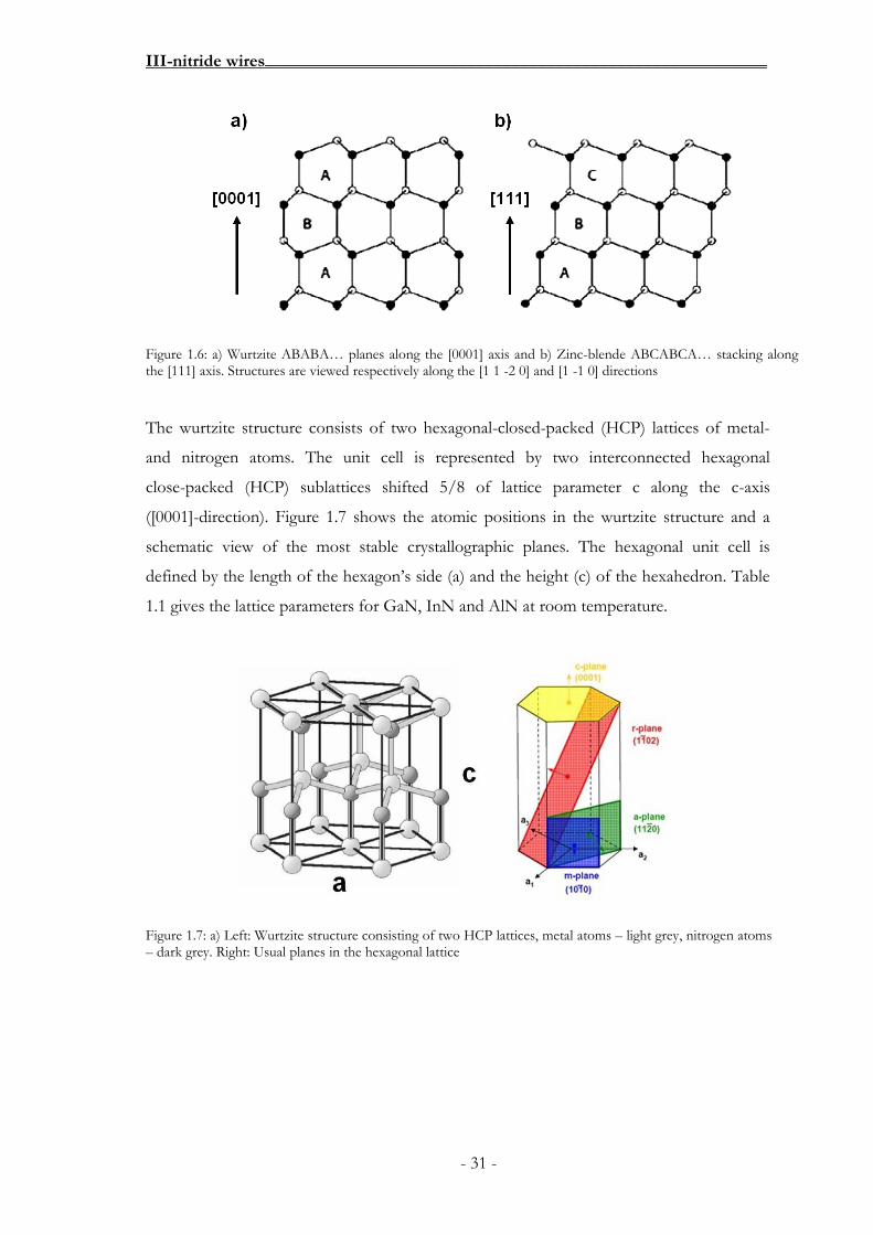
The wurtzite structure consists of two hexagonal-closed-packed (HCP) lattices of metal-
and nitrogen atoms. The unit cell is represented by two interconnected hexagonal
close-packed (HCP) sublattices shifted 5/8 of lattice parameter c along the c-axis
([0001]-direction). Figure 1.7 shows the atomic positions in the wurtzite structure and a
schematic view of the most stable crystallographic planes. The hexagonal unit cell is
defined by the length of the hexagon’s side (a) and the height (c) of the hexahedron. Table
1.1 gives the lattice parameters for GaN, InN and AlN at room temperature.
Figure 1.6: a) Wurtzite ABABA… planes along the [0001] axis and b) Zinc-blende ABCABCA… stacking along the [111] axis. Structures are viewed respectively along the [1 1 -2 0] and [1 -1 0] directions
Figure 1.7: a) Left: Wurtzite structure consisting of two HCP lattices, metal atoms – light grey, nitrogen atoms – dark grey. Right: Usual planes in the hexagonal lattice
III-nitride wires_________________________________________________________
- 32 -
For alloys as InxGa1-xN and AlxGa1-xN, the lattice parameters are usually approximated by
Vegard’s law [Vegard21].
(eq. 1)
BANBA x)c(1xccx1x
−+=−
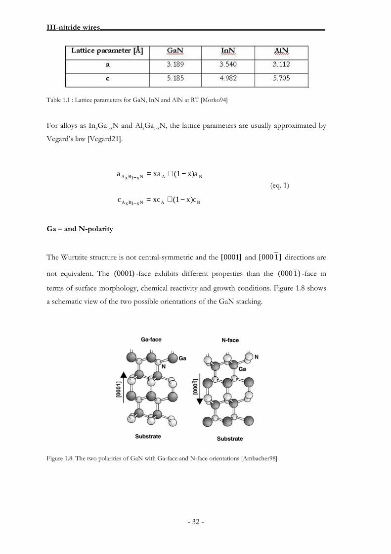
Ga – and N-polarity
The Wurtzite structure is not central-symmetric and the ]0001[ and ]1000[ directions are
not equivalent. The )0001( -face exhibits different properties than the )1000( -face in
terms of surface morphology, chemical reactivity and growth conditions. Figure 1.8 shows
a schematic view of the two possible orientations of the GaN stacking.
Table 1.1 : Lattice parameters for GaN, InN and AlN at RT [Morko94]
Figure 1.8: The two polarities of GaN with Ga-face and N-face orientations [Ambacher98]
BANBA x)a(1xaax1x
−+=−

III-nitride wires_________________________________________________________
- 33 -
Spontaneous and piezoelectric polarisation
Nitrogen atoms exhibit a larger electro-negativity than metal atoms and therefore the bond
has an electric dipole. Along the [0001] direction, this charge distribution cannot be
compensated, and leads to a macroscopic spontaneous polarisation in nitride materials
reported in Table 1.2 for GaN, InN and AlN. The resulting electric fields can reach up to
several MV/cm in (0001) orientated quantum wells [Bernardini97].
GaN InN AlN
Psp [C/cm2] -0.029 -0.032 -0.081
Table 1.2 : Calculated spontaneous polarisation for GaN, InN and AlN [Bernardini97]
Strain can modify the atomic position and the charge distribution in the crystalline lattice
and can also lead to a piezoelectric polarisation. The piezoelectric polarisation in wurtzite
III-nitrides can be calculated with the following equation [Romanov06]:
×
=
6
5
4
3
2
1
333131
15
15
000
00000
00000
εεεεεε
eee
e
e
Ppz
r (eq. 2)
eij are the piezoelectric coefficients of the material and (ε1, ε2, … ε6)T the stress tensor.
GaN InN AlN Ref.
e15 [C/m2] -0.30 - -0.48 [Ambacher00]
e31 [C/m2] -0.49 -0.57 -0.60 [Bernardini97]
e33 [C/m2] 0.73 0.97 1.46 [Bernardini97]
Table 1.3 Calculated piezo electric constants e15, e31 and e33 for GaN, InN and AlN
For a growth direction along c, ε
−= 33
33
13312 e
C
CePpz where 00 /)( aaa −=ε (a0 and a
are the in-plane lattice constants of the unstrained and strained crystals).

III-nitride wires_________________________________________________________
- 34 -
The vector sum of the spontaneous and the piezoelectric polarisation gives the overall
polarisation in the crystal.
Discontinuities of the polarisation vector at interfaces lead to charge accumulation,
which in turn generates internal electrical fields. Such large fields have huge influence on
the optical properties of the structure. The most obvious one is the Quantum Confined
Stark Effect (QCSE) which will be discussed later since it introduces a red shift in the
emission energy of quantum wells.
Dislocations
Dislocations in nitrides are generated via plastic relaxation of the material. They are
extended linear defects propagating along specific directions and defined by their Burgers
and line vectors10. They are known to decrease the performance of optoelectronic devices
by creating non-radiative recombination centres [Sugahara98]. The lattice mismatch
between the substrate and the overgrowth can create “misfit dislocations”. When they
propagate to the surface, they are called threading dislocations (TDs) [Kapolnek95,
Chien96, Ponce96]. Three types of dislocations are usually distinguished: edge, screw and
mixed.
In edge-type dislocations, the Burgers vector is perpendicular to the dislocation line. A
half-plane perpendicular to br
is inserted into the crystal as illustrated in Figure 1.9.
10 The dislocation line separates the unaffected part of the crystal from the shifted region. It represents the line of propagation of the dislocation. The Burgers vector is defined as the vectorial difference between two closed lattice circuits: one in the deformed crystal that surrounds the dislocation line and a similar one in the crystal without deformation. It is invariable around all points of a given dislocation and independent on the chosen closed circuit. Its module carries information about the shift magnitude and the strain energy released by the formation of the dislocation.
Figure 1.9: Edge-type dislocation with br
perpendicular to the dislocation line

III-nitride wires_________________________________________________________
- 35 -
In the case of wurtzite nitrides they lie in the ( )0011 planes and their line is along the
[0001] direction. The Burgers vector is typically 1/3 >< 1021 . They mainly occur at the
first stage of the growth when the material coalesces to a 2D layer [Hiramatsu91,
Heying96].
Screw-type dislocations present dislocation lines parallel to the Burgers vector
<0001>. Two regions are shifted with respect to each other separated by the dislocation
line (Figure 1.10). Like the edge-type dislocation, the screw-type dislocation lies in the
( )0011 planes. The Burgers vector is along the [ ]0001 direction.
A combination of these two dislocation types is called a mixed dislocation. An
example of a mixed dislocation is given in Figure 1.11. The dislocation is of the screw-type
when it enters the crystal in A and leaves the crystal as an edge-type dislocation in B. In
GaN, the Burgers vector is usually 1/3 >< 3211 .
Figure 1.10: Screw-type dislocation with br
parallel to the dislocation line
Figure 1.11: Mixed dislocation: a combination of Screw-type and edge-type dislocation
III-nitride wires_________________________________________________________
- 36 -
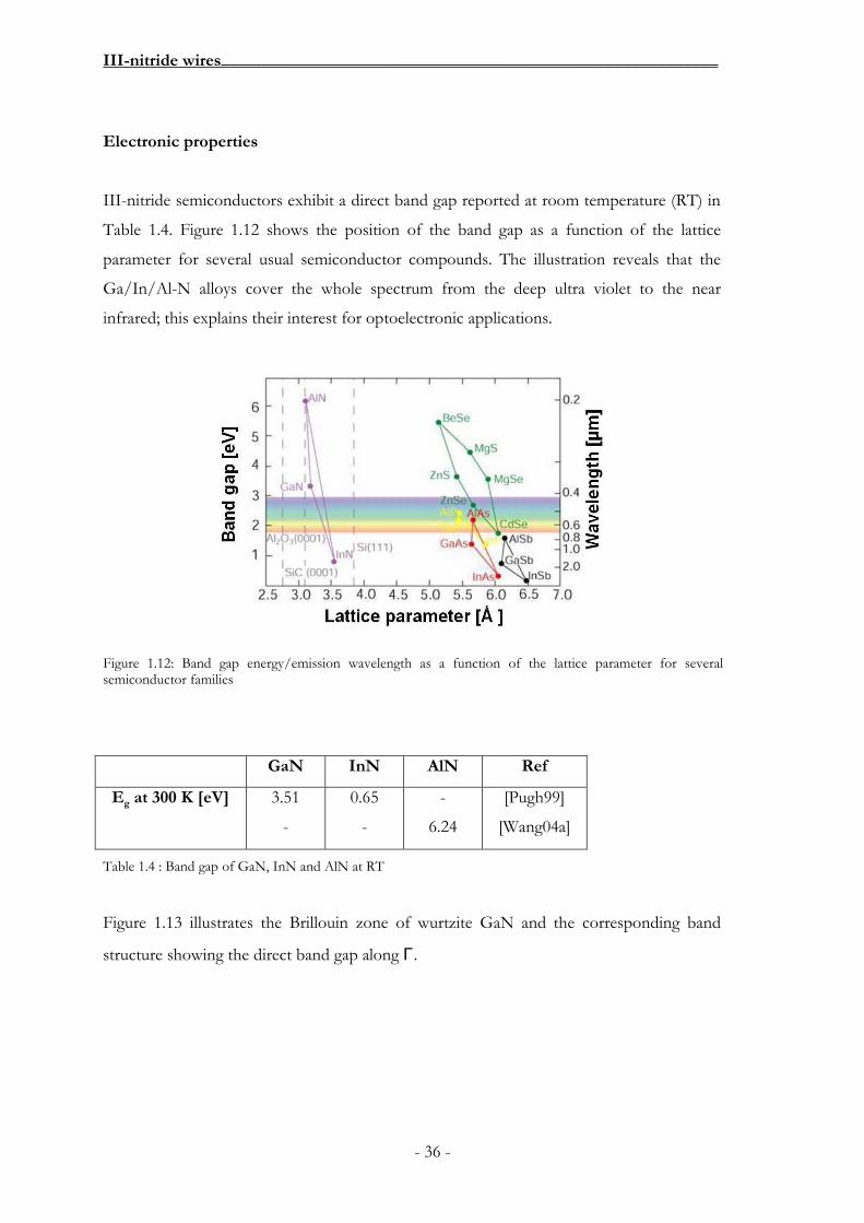
Electronic properties
III-nitride semiconductors exhibit a direct band gap reported at room temperature (RT) in
Table 1.4. Figure 1.12 shows the position of the band gap as a function of the lattice
parameter for several usual semiconductor compounds. The illustration reveals that the
Ga/In/Al-N alloys cover the whole spectrum from the deep ultra violet to the near
infrared; this explains their interest for optoelectronic applications.
GaN InN AlN Ref
Eg at 300 K [eV] 3.51
-
0.65
-
-
6.24
[Pugh99]
[Wang04a]
Table 1.4 : Band gap of GaN, InN and AlN at RT
Figure 1.13 illustrates the Brillouin zone of wurtzite GaN and the corresponding band
structure showing the direct band gap along Γ.
Figure 1.12: Band gap energy/emission wavelength as a function of the lattice parameter for several semiconductor families

III-nitride wires_________________________________________________________
- 37 -
The variation of the band gap with temperature is given by Varshni’s law [Varshni67].
Tβ
αT(0)E(T)E
2
gg +−= (eq. 3)
Eg(0) is the band gap energy at 0 K. The parameters α and β are tabulated, taking into
account the electron-phonon interaction. As shown in Table 1.5, the red shift between 0 K
and 300 K is about -68, -66, -96 meV for GaN, InN and AlN respectively.
Table 1.5 : Calculated values for Eg(0) and Varshni’s parameters (α and β) specifying the calculated band gap at RT
Figure 1.13: a) Brillouin zone of wurtzite GaN [www.ioffe.ru/SVA/NSM/] and b) its band structure [Bloom74]
Eg(0) [eV] α [meV/K] β [K] Eg (300 K)
[eV]
Ref.
GaN 3.489
3.492
0.887
0.531
0.909
874
432
830
3.421
3.426
[Leroux99]
[Tripathy99]
[Vurgaftman03]
InN 0.69 0.414 454 0.641 [Walukievicz04]
AlN 6.126 1.799
1.999
1462
1429
6.03 [Guo94]
[Vurgaftman03]

III-nitride wires_________________________________________________________
- 38 -
The band gap of ternary alloys AxB1-xN is usually calculated by the following formula:
ABNBN
gANg
NBAg x)bx(1xEx)E(1(x)E x1x −−+−=− (eq. 4)
b denotes the bowing parameter [Wu03].
b(eV) Ref.
InxGa1-xN
1.782 ± 0.076
1.916 ± 0.068
1.440 ± 0.000
[Liou05]
[Liou05]
[Caetano07]
AlxGa1-xN
0.353 ± 0.024
0.341 ± 0.035
0.351 ± 0.043
[Kuo02]
[Liou05]
[Liou05]
Table 1.6: Values of the bowing parameters for InGaN and AlGaN alloys
1.3.2. Properties and applications of III-nitride nanowires
The application of III-nitride nanowires, especially GaN nanowires, range from the
fabrication of optical devices as nanowire-based LEDs [Kim04, Qian05] and optically
pumped nanowire-based lasers [Qian08] to high electron mobility transistors [Li06b].
Sensor fabrications based on III-nitride nanowires, as Au [Dobrokhotov06] or DNA
[Simpkins07] functionalised GaN nanowires have not been developed as far by now.
1.3.2.1. GaN wires
GaN (nano)wires have been fabricated by MBE and MOCVD with both catalyst and
non-catalyst methods. Their diameter ranges from tens of nanometers up to more than a
micrometer. They exhibit wurtzite structure with hexagonal cross section, i.e. for a growth
along the c-direction, but nanowires grown by the catalyst-assisted MOCVD preferentially
grow along the a-axis with a triangular cross-section [Kuykendall03]. The wires are
generally strain-free due to surface relaxation and exhibit good optical quality. For MBE

III-nitride wires_________________________________________________________
- 39 -
catalyst-free wires, a near band edge (NBE) FWHM of 1.26 meV at low temperature has
been reported [VanNostrand06].
The coalescence of GaN wires has been used to grow free standing c-plane GaN
layers [Bougrioua07]. This technique overcomes the lattice-mismatch occurring at the
interface between the 2D layer and the substrate. A similar approach, using catalyst assisted
MOCVD growth has been used to grow free standing a-plane GaN [Li09].
The covering of the full 0.2 – 2 µm emission range with III-nitride compounds
(shown in Figure 1.12) can be obtained by controlling the growth of ternary InGaN and
AlGaN alloys. In contrast to the huge amount of publications concerning the growth of
GaN wires, InN/InGaN and AlN/AlGaN wires are rarely reported.
1.3.2.2. InN alloy based nanowires
Pure InN/InGaN-based nanowires
Kuykendall et al. [Kuykendall07] demonstrated the growth of InGaN nanowires with an
indium concentration of up to 90 % by CVD. Chloride precursors has been used allowing
a growth temperature between 600 – 650 °C suitable for the incorporation of high indium
concentrations. Figure 1.14 shows SEM images of the resulting nanowire growth. For low
indium concentrations, the wires exhibit a diameter of several tens of nm and a needle-like
shape. For high indium concentrations (75% - 90%), the nanowires become thicker and
reach a diameter of about 100 nm with a hexagonal cross section. No phase separation has
been observed and optical measurements revealed the full tunability of the band gap from
3.4 to 1.25 eV (see the plot in Figure 1.14).
Figure 1.14: Growth of InGaN alloy wires by CVD (left). Band edge energy as function of the alloy composition (right) [Kuykendall07]
III-nitride wires_________________________________________________________
- 40 -
With increasing indium molar fraction a broadening of the emission peak is observed (not
displayed here). These results have been interpreted as promising for the development of
nanowire-based light emitting devices covering the full visible spectrum up to the near
infrared.
1.3.2.3. InGaN/GaN-based nanowire heterostructures
Like in 2D materials, InGaN/GaN heterostructures are the main building block for
nanowire-based LEDs, lasers and photovoltaic devices. The experimental realisations are
still at the beginning of their development but they already shows a trend for potential
commercial applications. In this section, a short overview on the basic properties of these
devices will be given.
LED
Kim et al. [Kim04] demonstrated the fabrication of a longitudinal InGaN/GaN nanowire
LED assembly. The wires are grown directly on a 2D GaN template by metal organic
hydride vapour phase epitaxy (MO-HVPE) without the use of catalysts or pre-patterned
substrates. The nanowires consist in stacking n-type GaN at the bottom followed by
In0.25Ga0.75N/GaN superlattice and by p-type GaN on top. The whole array is buried in
spin-on glass (SOG) after the growth in order to electrically isolate the individual wires.
The top of the resulting 2D structure is covered with a transparent Ni/Au electrode (see
Figure 1.15 a)). A thick Ni/Au electrode (p-pad) is deposited on the surface and the n-
contact, consisting of Ti/Al electrodes, is deposited on n-type GaN after etching. This
vertical design leads to an efficient flow of the injected carriers confined inside the wires.
Figure 1.15 b) shows the light-output power as a function of the applied current.

III-nitride wires_________________________________________________________
- 41 -
Another important result based on single GaN nanowires has been obtained by
Qian et al. [Qian05]. Triangular shaped n-doped GaN nanowires grown by the catalyst-
assisted MOCVD method have been used as a template for the deposition of an
InGaN/GaN/p-AlGaN/p-GaN shell structure (see Figure 1.16 a)). The emission
wavelength of the InGaN shell is controlled by changing the indium concentration in the
InGaN active layer. The inset in Figure 1.16 b) shows a SEM image of a single contacted
nanowire with the n- and p-pads. The current versus voltage plot demonstrates the
rectification behaviour expected for the n-p-junction. Figure 1.16 c) shows the normalised
electroluminescence (EL) emission for wires having different indium concentrations. The
wavelength ranges from 367 nm for an In-concentration of about 1 % to 577 nm for an In-
concentration of 35 % in the active layer. Figure 1.16 d) shows optical microscopy images
of the structure under a forward bias of 9 and 11 V respectively. The emission is mainly
observed at the top of the wire, giving evidence of light guiding inside the nanowire.
Figure 1.15: a) Schematic view of the longitudinal InGaN/GaN MQW LED b) Light-output power as the function of the applied current. The inset shows the light emission of the device under electrical injection [Kim04]

III-nitride wires_________________________________________________________
- 42 -
Laser
Qian et al. [Qian08] also demonstrated lasing on single GaN nanowires with an
InGaN/GaN MQW core-shell heterostructure. As before [Qian05], the GaN core wire
was grown by catalyst-assisted MOVPE growth resulting in a triangular cross section. This
step is immediately followed by the InGaN/GaN MQW (x 26) shell deposition. A
schematic view of the structure is given in Figure 1.17 a). Dark-field cross-section STEM
revealed the MQW structure growing along the ( )0111 facets, but not along the third facet
of the triangle, i.e. the (0001) facet in which the growth rate is very small. The nanowire is
optically pumped and shows lasing for power densities larger than 700 kW/cm2. Figure
1.17 c) shows the PL spectra of four nanowires with different In-concentrations in the
QWs. The emission lines span from 381.1 nm for the lowest indium concentration (5%) up
to 477.9 nm for the highest concentration (23 %). An electrically pumped nitride nanowire
based laser is not yet reported in the literature.
Figure 1.16: a) Schematic view of single nanowire LED structures based on an n-GaN core wire with InGaN/i-GaN/p-AlGaN/p-GaN shells, b) Connected wire with n- and p-pads and corresponding I-V curve, c) Normalised EL spectra for different In-concentrations, d) Optical microscopy images for 9 and 11 V forward bias [Qian05]

III-nitride wires_________________________________________________________
- 43 -
Photovoltaic device
Core/shell n-GaN/InGaN/p-GaN heterostructures also offer potential applications in
photovoltaics as demonstrated by Dong et al. [Dong09]. The n-GaN core wire grown by
the catalyst-assisted technique described by Qian et al. [Qian05, Qian08] is followed by the
deposition of an InGaN shell and is finished with p-GaN (see Figure 1.18 a)). For the
electrical measurements, the wire is etched down to the n-GaN core on one side and then
contacted in the horizontal configuration (see Figure 1.18 b)).
Figure 1.17: a) Schematic view of a GaN/InGaN MQW (x 26) heterostructure grown around a GaN wire template. b) TEM cross-section and diffraction pattern. c) PL emission for wires with different indium concentrations in the MWQs [Qian08].

III-nitride wires_________________________________________________________
- 44 -
I-V measurements were carried out under illumination with 1-sun AM 1.5G light source11,
imitating the solar spectrum after passing the atmosphere – the standard conditions for
solar cell testing. Figure 1.18 c) shows the I-V curves for nanowires with different
In-concentrations in the InGaN shell. The absorption correspond to UV (371 nm), purple
(396 nm), blue (457 nm) and green (556 nm) wavelengths. The threshold voltage increases
with decreasing In-concentration due to the InGaN band-gap increase. Under illumination,
the open circuit voltage Voc is increased from 1 V to 2 V with decreasing In-concentration.
The short circuit current density ranges from 0.059 to 0.39 mA/cm2. This change is not
attributed to the change of the indium concentration, but to the anisotropic spectrum of
the light source.
The resulting yield is small compared to 2D devices and a lot of efforts have still to
be made to optimise these devices.
11 1 sun AM 1.5 G is defined as the solar irradiance reaching the ground after passing the earth’s atmosphere at an angle of 48.2 ° with respect to the zenith.
Figure 1.18: a) Schematic cross-section of n-GaN/InGaN/p-GaN core/shell nanowires and corresponding band diagram. b) Electrical contact schematic and corresponding SEM image. c) I-V curve for nanowires with different indium concentrations with and without illumination [Dong09].

III-nitride wires_________________________________________________________
- 45 -
1.3.2.4. AlN alloy-based nanowires
AlN based nanowires
The growth of AlN nanowires has been achieved by Yazdi et al. [Yazdi09] by a MBE self-
assembled VS approach on SiC without catalysts. Figure 1.19 a) shows two SEM images at
different magnifications. The wires grow along the [0001] direction and are
mono-crystalline. Diameters between 40 nm and 500 nm were observed depending on the
growth conditions. The nanowires can reach a length of more than 100 µm. The nanowires
grow on hexagonal shaped islands and exhibit a hexagonal shape and show no tendency to
grow laterally after having emerged from the pyramids. CL measurements on single wires
revealed their optical properties (Figure 1.19 b)). The spectrum exhibits the AlN near band
edge emission at 209 nm (5.93 eV) (indicated by the black arrow) and a broad defect band
centred at 374 nm (3.3 eV) attributed to oxygen impurity vacancy complexes. The optical
properties clearly need to be improved.
More recently, the growth of catalyst-free AlN nanowires has been achieved by
plasma-assisted MBE on SiO2/Si (100) by taking advantage of the Volmer–Weber growth
mode of AlN on amorphous SiO2 [Landré2010]. Using a combination of high resolution
transmission electron microscopy (HRTEM) and Raman spectroscopy, it becomes evident
that AlN nanowires are completely relaxed. Elastic strain relaxation of AlN nanowires has
Figure 1.19: a) MBE grown catalyst-free AlN wires, b) CL spectra of an AlN wire with band-edge emission (black arrow) and a strong defect band [Yazdi09]

III-nitride wires_________________________________________________________
- 46 -
been further confirmed by photoluminescence experiments showing in addition that
spectra are dominated by near-band-edge emission (a defect band is not discussed).
With the MOCVD technique, Su et al. [Su05] reported the growth of AlGaN
nanowires by catalyst-assisted growth on a poly-crystalline alumina sample coated with a
several Ǻ thick Ni layer. The wires grow along the a-direction and exhibit a triangular shape
with a diameter around several tens of nanometers. A change of the alloy composition
along the cross-section of the wires with a strong Al content in the shell and a high Ga
content in the core was observed.
1.3.2.5. AlGaN/GaN-based nanowire heterostructures
GaN/AlN quantum dots
The growth of GaN/AlN quantum dots (QDs) on top of GaN nanowires (about 20 nm in
diameter) was demonstrated by MBE by Songmuang et al. The general idea is to grow GaN
dots in between AlN barriers as shown in Figure 1.20 (see experimental details in
[Renard08]). The nanowire geometry allows the detailed study of the photoluminescence of
single QDs [Renard08, Renard09] with a low background level compared to usual QDs
embedded in 2D structures.
Figure 1.20: a) Schematic view of a GaN nanowire with an AlN/GaN/AlN heterostructure on top of a c-oriented GaN nanowire, b) TEM image of the top region containing the QD heterostructure, c) corresponding µPL spectra of the heterostructure [Renard08]
III-nitride wires_________________________________________________________
- 47 -
Microcavity
Ristic et al. [Ristic05] demonstrated the catalyst-free MBE growth of longitudinal
AlGaN/GaN nanocavities in GaN nanowires. The structures were grown by a self-
assembled approach on Si(111) starting with the growth of GaN nanowires. The active
region consisting of GaN multiple quantum disks (3 nm thick GaN) embedded in
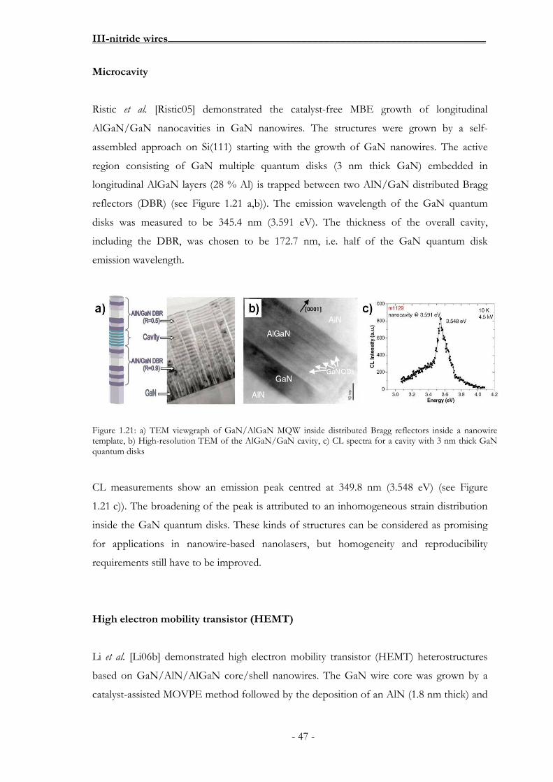
longitudinal AlGaN layers (28 % Al) is trapped between two AlN/GaN distributed Bragg
reflectors (DBR) (see Figure 1.21 a,b)). The emission wavelength of the GaN quantum
disks was measured to be 345.4 nm (3.591 eV). The thickness of the overall cavity,
including the DBR, was chosen to be 172.7 nm, i.e. half of the GaN quantum disk
emission wavelength.
CL measurements show an emission peak centred at 349.8 nm (3.548 eV) (see Figure
1.21 c)). The broadening of the peak is attributed to an inhomogeneous strain distribution
inside the GaN quantum disks. These kinds of structures can be considered as promising
for applications in nanowire-based nanolasers, but homogeneity and reproducibility
requirements still have to be improved.
High electron mobility transistor (HEMT)
Li et al. [Li06b] demonstrated high electron mobility transistor (HEMT) heterostructures
based on GaN/AlN/AlGaN core/shell nanowires. The GaN wire core was grown by a
catalyst-assisted MOVPE method followed by the deposition of an AlN (1.8 nm thick) and
Figure 1.21: a) TEM viewgraph of GaN/AlGaN MQW inside distributed Bragg reflectors inside a nanowire template, b) High-resolution TEM of the AlGaN/GaN cavity, c) CL spectra for a cavity with 3 nm thick GaN quantum disks

III-nitride wires_________________________________________________________
- 48 -
AlGaN shell. These wires are grown along the a-direction and have a triangular cross-
section with non-equivalent facet planes (see indexation in Figure 1.22 a)).
This nanowire geometry was used to fabricate horizontal field effect transistors (FETs) (see
the schematic at the bottom of Figure 1.22). Transport measurements showed the
formation of a 2D electron gas with a very high electron mobility of 3100 up to 21 000 V/
for 300 K and 5 K respectively. Moreover a large on/off current ratio of 107 was reported
in this structure (compared to 2500 V/cm2 and 106 for an electron mobility and an on/off
current ratio respectively in current HEMT transistors).
1.4. Growth of gallium nitride wires
1.4.1. MBE growth
As illustrated by the previously presented applications, two main approaches have been
developed in MBE for the growth of gallium nitride nanowires: the catalytic way using
metal catalysts as Ni and Au to promote the vertical growth [Duan00, Lee04, Geelhaar07]
and the catalyst-free way [Calleja00, Tchernycheva07, Songmuang07, Landré08, Ristic08,
Aschenbrenner09].
Figure 1.22: a) Cross section TEM of a triangular nanowire with the GaN core and the AlN/AlGaN shells, b) High resolution TEM showing the 1.8 nm thick AlN layer between the GaN core and the AlGaN outer shell

III-nitride wires_________________________________________________________
- 49 -
1.4.1.1. Catalyst induced growth of GaN nanowires
The growth of GaN nanowires with metal catalysts is generally explained by the VLS
mechanism. One example of this catalyst-assisted approach is the growth of GaN
nanowires on c-plane sapphire reported by Geelhaar et al. [Geelhaar07]. The substrate is
covered ex situ by a thin (several Ǻ thick) layer of Ni and is then in situ annealed at 750 °C
for 15 min. Atomic force microscopy (AFM) measurements on a reference sample revealed
the formation of Ni islands on the substrate surface (dewetting phenomena).
The annealing is immediately followed by the GaN deposition at 730 °C leading to the
growth of perpendicularly oriented GaN nanowires with a length of about 2 µm and a
diameter between 50 and 70 nm (see Figure 1.23 a)). TEM images reveal the Ni catalyst on
top of the wire (see Figure 1.23 b)). The V/III ratio was found to be the key parameter for
the formation of wires. The nanowire growth (c-plane direction) is observed for
nitrogen-rich conditions (high nitrogen flow). Under Ga-rich conditions, the formation of
a 2D layer is observed. The growth rate is larger compared to the growth of 2D GaN.
The modelling of the VLS growth mechanism has been quite extensively developed
in the literature [Dubrovskii08 and forthcoming papers]. The growth starts with the
formation of a liquid metal droplet in which the semiconductor material is incorporated
directly from the gas phase. The material nucleates at the interface between the droplet and
the nanowire. In parallel, the material already deposited on the surface diffuses along the
wire’s side facets into the droplet and contributes to the wire growth (see Figure 1.24).
During the VLS growth, the catalyst droplet and the semiconductor form a liquid alloy
[Harmand07], whereas in some specific systems the catalyst may remain solid (it is named
Figure 1.23: GaN nanowire growth by MBE on a c-plane sapphire using a Ni catalyst: a) SEM cross-section, b) TEM image with the Ni catalyst on top of the wire. [Geelhaar07]
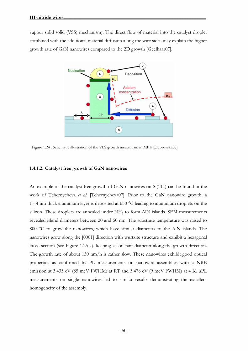
III-nitride wires_________________________________________________________
- 50 -
vapour solid solid (VSS) mechanism). The direct flow of material into the catalyst droplet
combined with the additional material diffusion along the wire sides may explain the higher
growth rate of GaN nanowires compared to the 2D growth [Geelhaar07].
1.4.1.2. Catalyst free growth of GaN nanowires
An example of the catalyst free growth of GaN nanowires on Si(111) can be found in the
work of Tchernycheva et al. [Tchernycheva07]. Prior to the GaN nanowire growth, a
1 - 4 nm thick aluminium layer is deposited at 650 °C leading to aluminium droplets on the
silicon. These droplets are annealed under NH3 to form AlN islands. SEM measurements
revealed island diameters between 20 and 50 nm. The substrate temperature was raised to
800 °C to grow the nanowires, which have similar diameters to the AlN islands. The
nanowires grow along the [0001] direction with wurtzite structure and exhibit a hexagonal
cross-section (see Figure 1.25 a), keeping a constant diameter along the growth direction.
The growth rate of about 150 nm/h is rather slow. These nanowires exhibit good optical
properties as confirmed by PL measurements on nanowire assemblies with a NBE
emission at 3.433 eV (85 meV FWHM) at RT and 3.478 eV (9 meV FWHM) at 4 K. µPL
measurements on single nanowires led to similar results demonstrating the excellent
homogeneity of the assembly.
Figure 1.24 : Schematic illustration of the VLS growth mechanism in MBE [Dubrovskii08]
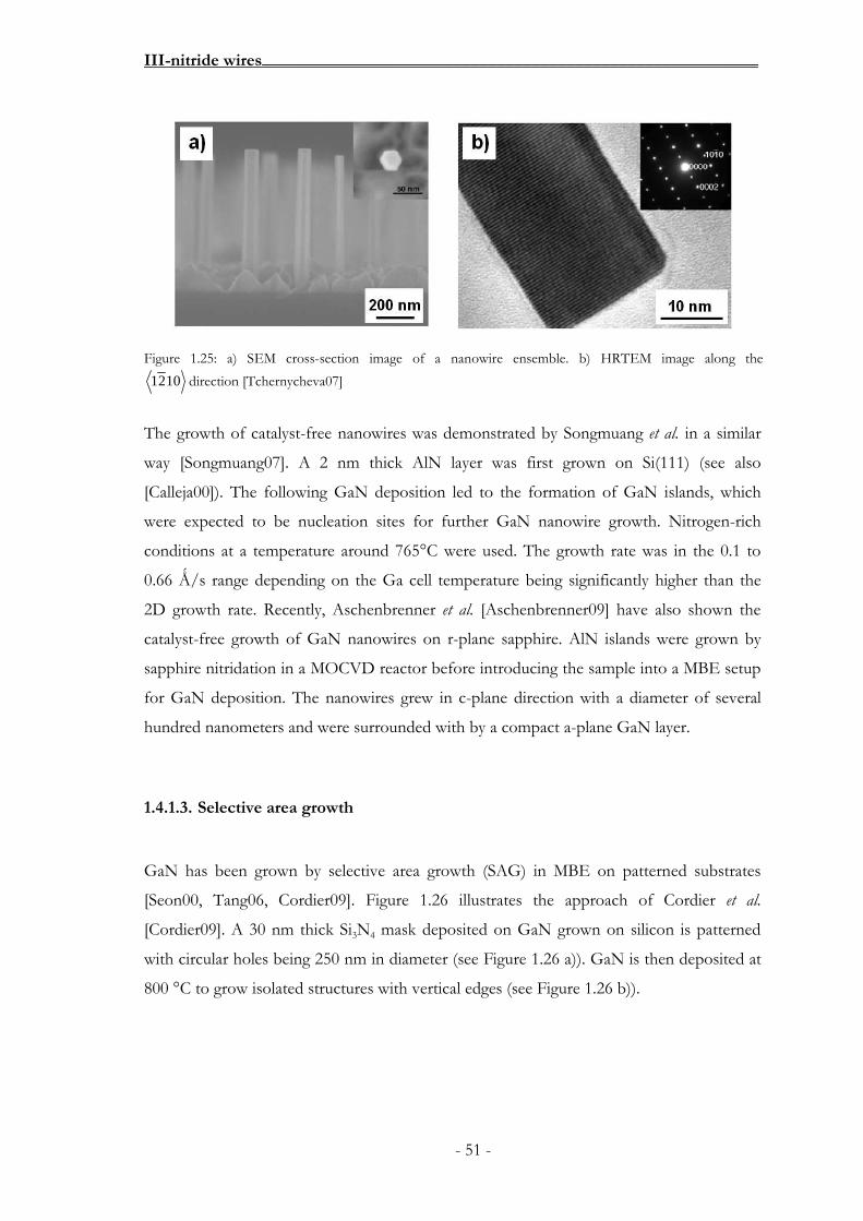
III-nitride wires_________________________________________________________
- 51 -
The growth of catalyst-free nanowires was demonstrated by Songmuang et al. in a similar
way [Songmuang07]. A 2 nm thick AlN layer was first grown on Si(111) (see also
[Calleja00]). The following GaN deposition led to the formation of GaN islands, which
were expected to be nucleation sites for further GaN nanowire growth. Nitrogen-rich
conditions at a temperature around 765°C were used. The growth rate was in the 0.1 to
0.66 Ǻ/s range depending on the Ga cell temperature being significantly higher than the
2D growth rate. Recently, Aschenbrenner et al. [Aschenbrenner09] have also shown the
catalyst-free growth of GaN nanowires on r-plane sapphire. AlN islands were grown by
sapphire nitridation in a MOCVD reactor before introducing the sample into a MBE setup
for GaN deposition. The nanowires grew in c-plane direction with a diameter of several
hundred nanometers and were surrounded with by a compact a-plane GaN layer.
1.4.1.3. Selective area growth
GaN has been grown by selective area growth (SAG) in MBE on patterned substrates
[Seon00, Tang06, Cordier09]. Figure 1.26 illustrates the approach of Cordier et al.
[Cordier09]. A 30 nm thick Si3N4 mask deposited on GaN grown on silicon is patterned
with circular holes being 250 nm in diameter (see Figure 1.26 a)). GaN is then deposited at
800 °C to grow isolated structures with vertical edges (see Figure 1.26 b)).
Figure 1.25: a) SEM cross-section image of a nanowire ensemble. b) HRTEM image along the
1021 direction [Tchernycheva07]
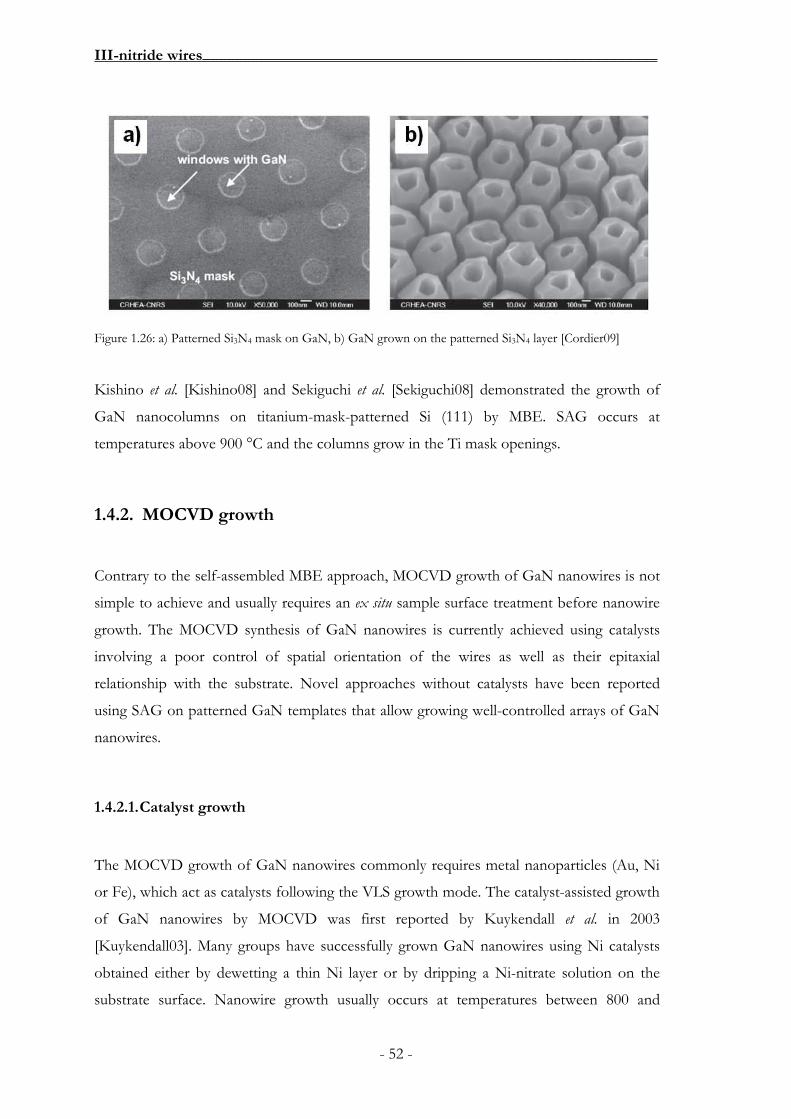
III-nitride wires_________________________________________________________
- 52 -
Kishino et al. [Kishino08] and Sekiguchi et al. [Sekiguchi08] demonstrated the growth of
GaN nanocolumns on titanium-mask-patterned Si (111) by MBE. SAG occurs at
temperatures above 900 °C and the columns grow in the Ti mask openings.
1.4.2. MOCVD growth
Contrary to the self-assembled MBE approach, MOCVD growth of GaN nanowires is not
simple to achieve and usually requires an ex situ sample surface treatment before nanowire
growth. The MOCVD synthesis of GaN nanowires is currently achieved using catalysts
involving a poor control of spatial orientation of the wires as well as their epitaxial
relationship with the substrate. Novel approaches without catalysts have been reported
using SAG on patterned GaN templates that allow growing well-controlled arrays of GaN
nanowires.
1.4.2.1. Catalyst growth
The MOCVD growth of GaN nanowires commonly requires metal nanoparticles (Au, Ni
or Fe), which act as catalysts following the VLS growth mode. The catalyst-assisted growth
of GaN nanowires by MOCVD was first reported by Kuykendall et al. in 2003
[Kuykendall03]. Many groups have successfully grown GaN nanowires using Ni catalysts
obtained either by dewetting a thin Ni layer or by dripping a Ni-nitrate solution on the
substrate surface. Nanowire growth usually occurs at temperatures between 800 and
Figure 1.26: a) Patterned Si3N4 mask on GaN, b) GaN grown on the patterned Si3N4 layer [Cordier09]

III-nitride wires_________________________________________________________
- 53 -
1000 °C. Trimethylgallium (TMG) and ammonia are used as precursors. Figure 1.27 a)
shows nanowires grown on an ex situ gold-coated c-plane sapphire substrate. The
nanowires exhibit a triangular shape (see inset) indicating a growth direction along the non-
polar [210] direction and more rarely along the [100] direction.
PL measurements show a broad emission peak between 360 and 385 nm centred at 370 nm
(3.35 eV) at 5 K and 380 nm (3.26 eV) at 285 K. No yellow band could be observed, which
indicates good optical properties of the nanowires. Electrical measurements done on single
wires gave a carrier mobility of 65 cm2/Vs and a carrier concentration of 4 x 1018 cm-3.
A control of the crystalline direction of the nanowires was reported as a function of
the substrate nature. Catalyst growth on γ-LiAlO2 (100) and MgO (111) substrates resulted
in the growth of nanowires in the orthogonal [1-11] and [001] directions respectively
[Kuykendall04].
The growth of vertical catalysed nanowires is achieved using r-sapphire substrates
[Wang06]. As the vertical nanowires grow along the non-polar [210] direction, the same
group has succeeded in the growth of a-plane GaN templates by full coalescence in the
upper section of the nanowires [Li09].
The catalyst approach allows only the growth of GaN nanowire-based radial
heterostructures since indium and aluminium precursors suppress the catalytic process due
to a formation of stable chemical phases in the droplet. The growth of axial nitride
heterostructures is thus very difficult to accomplish using the conventional catalyst
approaches.
Figure 1.27: a) Gold catalysed GaN nanowires, b) TEM viewgraph and diffraction patterns of a single nanowire with a gold catalyst on top

III-nitride wires_________________________________________________________
- 54 -
1.4.2.2. Selective area growth
In SAG, pre-patterned substrates are applied for the growth of nanowires in order to
control their diameter, position and density independently. The patterning techniques may
be time-consuming and expensive, for example when e-beam lithography is required to
reach very high resolution.12 In the literature, interferometric lithography and porous
anodic alumina (PAA) templates have been used for the growth of GaN wires.
Hersee et al. [Hersee06] demonstrated the catalyst-free growth of GaN wires
through a patterned SiNx layer deposited by low pressure chemical vapour deposition
(LPCVD) on a 600 nm thick GaN template. The SiNx layer was patterned by
interferometric lithography and dry etching to obtain holes with diameters of about 220 nm
ordered in hexagonal lattice with a 500 nm period.
The GaN wires were grown at 1050 °C and with a reactor pressure of 133 mbar in
a mixture of hydrogen and nitrogen carrier gas in a P75 Veeco TurboDisk MOCVD
reactor. The V/III ratio was set to 1500 to ensure a proper filling of the holes before
switching the system to the “pulsed growth mode” where the precursors are injected
alternately. This technique prevents lateral growth of the wires after they emerged from the
holes.
The wires exhibit a hexagonal shape with a diameter matching the diameter of the
holes (see Figure 1.28 a)). The wires are well ordered in the patterned hexagonal lattice and
grow along the [0001] direction. It has been shown that they have a very low density of
threading dislocations (see Figure 1.28 b)). In this pioneer study, the optical properties of
the wires were not reported.
In the industry, glō AB13 founded by the Lund University’s Nanometer Structure
Consortium14 is a venture-backed, development-stage company focused on the
development and commercialisation of entirely new, highly energy efficient and very low
cost nanowire light-emitting diodes (nLED). This company is presently developing
GaN-based LEDs among several III-V systems, but has not publish their main results up
to now for intellectual property reasons.
12 Combined with the nanoimprint technique, molds can be reused to reach volume production. 13 GLO web site: http://www.glo.se/ 14 Lund University’s Nanometer Structure Consortium web site: http://nano.lth.se/

III-nitride wires_________________________________________________________
- 55 -
Deb et al. [Deb05] demonstrated the patterning of SiOx using intermediate porous anodic
alumina (PAA). The process starts with the deposition of a 5 µm thick layer of GaN by
HVPE on a c-plane sapphire followed by the deposition of a 60 nm thick layer of SiOx. A
one micrometer thick Al layer is deposited and oxidised by anodisation to form a
nanoporous oxide layer with a pore diameter between 10 and 15 nm. The pore diameter is
increased to 60 nm by etching in H3PO4, and the pattern is then transferred to the SiOx
layer by SF6/O2 reactive ion etching (see Figure 1.29 a)).
The remaining PAA is removed by H3PO4. For the GaN nanowire growth, the ammonia
and TMG are used with a V/III ratio of 1500. The growth is carried out for 5 minutes
corresponding to a film thickness of 100 nm for 2D growth. The resulting nanowire height
is in the same order of magnitude. The remaining SiOx layer is finally removed from the
sample by means of hydrofluoric acid (HF). The nanowires (Figure 1.29 b)) are grown
Figure 1.28: a) GaN nanowires grown on a patterned template, b) TEM viewgraph of the nanowires [Hersee06]
Figure 1.29: a) Transfer of porous alumina patterning to a SiOx layer by reactive ion etching, b) GaN nanowires grown on a GaN layer by selective area growth with a SiOx mask (removed in this figure) [Deb05]

III-nitride wires_________________________________________________________
- 56 -
along the c-direction in epitaxial relationship with the underlying GaN template. As in the
previous case, the density of threading dislocations is quite low with this method and the
optical properties are not described in detail.
1.5. Conclusions
The huge interest in nanowires in the past ten years has been reviewed in this chapter to
show their role in fundamental research and potential applications. In this context, the
growth of GaN nanowires and GaN nanowire based heterostructures is particularly
interesting for opto- and nanoelectronics with the demonstration of nanowire-based LEDs
[Kim04, Qian05], optically pumped single nanowire lasers [Qian08] and HEMTs [Li06b] as
worked out in this manuscript. Furthermore, these 1D structures are of interest in
fundamental research of confinement effects of electron gases as well as single electron
transistors.
The growth of GaN nanowires with diameters from some tens up to several hundreds of
nanometres is widely reported and has also been achieved by catalyst-assisted growth
[Duan00, Kuykendall03, Geelhaar07] by MBE and MOCVD as well as catalyst-free
approaches by MBE [Calleja00, Tchernycheva07, Songmuang07, Landré08, Ristic08,
Aschenbrenner09]. Catalyst-free approaches by MOCVD could be grown by means of
SAG [Deb05, Hersee06]. InGaN wires with an In-concentration up to 90 %
[Kuykendall07] and AlN wires [Yazdi09, Landré2010] have been grown by MOCVD and
MBE respectively. These results still are outnumbered by the results dealing with the
growth of GaN wires.
Very different approaches have been explored to grow these materials with or without the
use of catalysts, and with MBE, HVPE and MOCVD growth techniques. From the
chemical point of view, the non-catalytic way prevents contamination that may degrade the
physical properties of the wires. From the morphological point of view, the selective area
growth of nitride-wire heterostructures (independently controlling the size, position and
density) has been reported both by MOCVD and MBE but suffers from complexity in the
template preparation. In MBE, the very convenient self-organized growth method without
catalyst is routinely being developed for nitride nanowires by several groups in the world
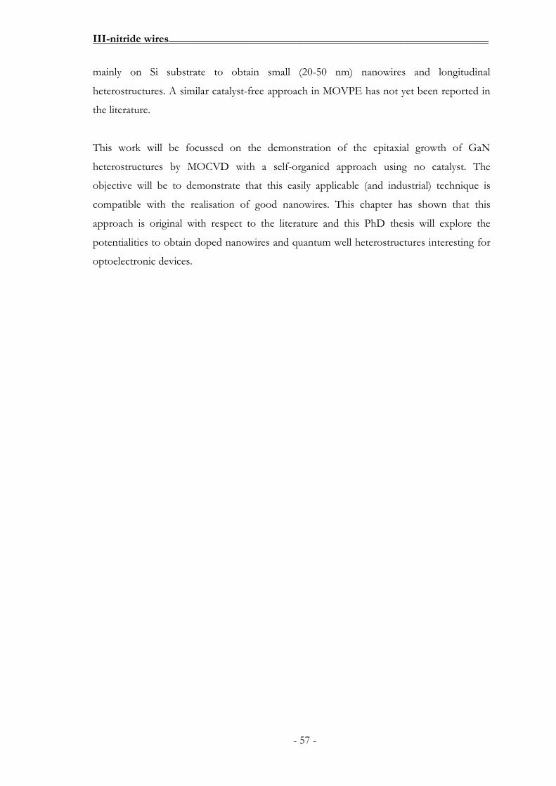
III-nitride wires_________________________________________________________
- 57 -
mainly on Si substrate to obtain small (20-50 nm) nanowires and longitudinal
heterostructures. A similar catalyst-free approach in MOVPE has not yet been reported in
the literature.
This work will be focussed on the demonstration of the epitaxial growth of GaN
heterostructures by MOCVD with a self-organied approach using no catalyst. The
objective will be to demonstrate that this easily applicable (and industrial) technique is
compatible with the realisation of good nanowires. This chapter has shown that this
approach is original with respect to the literature and this PhD thesis will explore the
potentialities to obtain doped nanowires and quantum well heterostructures interesting for
optoelectronic devices.

- 58 -
Chapter 2

- 59 -
2. Bi-dimensional growth of GaN by
MOVPE
This PhD project started with the installation of the first metal-organic chemical vapour
phase deposition (MOCVD) setup in the laboratory. Before the development of the GaN
wire growth, it was mandatory to validate this setup by basic bi-dimensional growth.
After a short introduction of the mechanisms involved in MOVPE and a
description of our setup, this chapter will deal with the characterisation of bi-dimensional
GaN layers and their n- and p-doping controls as well as the growth of AlGaN single layers
and InGaN multi quantum wells (MQWs). A blue LED structure was chosen as a
demonstrator combining most of these building blocks. The contacted device shows an
electroluminescence emission, demonstrating our capacities to grow this type of materials.
2.1. Introduction to the MOVPE process
MOVPE was developed as a technique for deposition of compound semiconductors in the
1960s and is nowadays widely used to grow many III/V materials (especially III-nitrides) to
fabricate semiconductor devices such as LEDs and laser diodes. In contrast to MBE,
MOVPE does not require ultra-high vacuum (UHV) conditions and can achieve higher
growth rates. The throughput can reach a capacity of more than sixty 2” wafers15, making
this technique interesting for industrial mass production. The homogeneity over large
surfaces and short process time are the main advantages compared to other growth
techniques.
The MOVPE growth process is highly complex because it is governed by thermodynamics,
mass and heat transport, chemical reactions of the precursors and surface
adsorption/diffusion. Figure 2.1 a) schematically illustrates the mechanisms involved in a
MOVPE reactor chamber. The precursors injected into the reactor are transported in a 15 Aixtron planetary reactor.

Bi-dimensional growth of GaN by MOVPE__________________________________
- 60 -
carrier gas flow in the direction of the sample surface and undergo chemical reactions. The
products (detailed below in this chapter), are adsorbed on the sample surface and may
diffuse over the substrate until they are either finally deposited or desorbed. In this case,
they leave the reactor chamber through the exhaust with the carrier-gas flow. The following
list shows the important processes involved during MOVPE growth:
• Transport of the precursors
• Thermal decomposition of the precursors in the gas phase
• Gas phase reactions forming intermediate products
• Adsorption of the intermediate products onto the substrate surface
• Diffusion of the products
• Evaporation of the products
• Surface diffusion and lattice incorporation of the intermediate products
• Desorption of incorporated material
• Transport of the products, intermediate products and precursors out of the reactor
The MOVPE process can be divided into three main regimes (see Figure 2.1 b)). At low
temperature, the growth rate is kinetically limited and directly depends on the reactor
temperature. The speed of chemical reactions and the rate of the product formation
determine the growth rate. For higher temperatures, the growth becomes transport limited.
In this regime, the growth rate is independent of the temperature and only depends on the
amount of materials reaching the surface. In this regime, the growth rate is constant all
throughout the temperature range. If the reactor temperature is still increased, the materials
start to be evaporated from the surface and the growth rate is decreased.
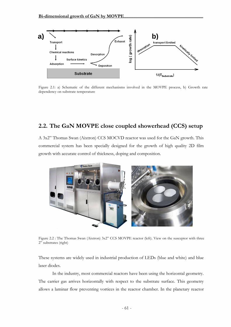
Bi-dimensional growth of GaN by MOVPE__________________________________
- 61 -
2.2. The GaN MOVPE close coupled showerhead (CCS) setup
A 3x2” Thomas Swan (Aixtron) CCS MOCVD reactor was used for the GaN growth. This
commercial system has been specially designed for the growth of high quality 2D film
growth with accurate control of thickness, doping and composition.
These systems are widely used in industrial production of LEDs (blue and white) and blue
laser diodes.
In the industry, most commercial reactors have been using the horizontal geometry.
The carrier gas arrives horizontally with respect to the substrate surface. This geometry
allows a laminar flow preventing vortices in the reactor chamber. In the planetary reactor
Figure 2.1: a) Schematic of the different mechanisms involved in the MOVPE process, b) Growth rate dependency on substrate temperature
Figure 2.2 : The Thomas Swan (Aixtron) 3x2” CCS MOVPE reactor (left). View on the susceptor with three 2” substrates (right)
a) b)

Bi-dimensional growth of GaN by MOVPE__________________________________
- 62 -
design, the susceptor rotation smoothes concentration and temperature gradients which
may induce growth inhomogeneities.
The vortices, which generally occur in standard vertical reactors like quartz tubes are
leading to deposition inhomogeneities (especially in the outer parts of the susceptor). They
are eliminated in the CCS design by the precursor injection through a showerhead, which is
the reactor lid mounted on top of the reactor (see Figure 2.3). The showerhead is close
(11 mm) to the substrates and is designed to enable precursors to be separated right up to
the point where they are injected into the reactor through a multiplicity of small tubes. The
precursors are injected into the reactor chamber through separate orifices in the
showerhead in order to create a very uniform distribution of reagent gases (without
vortices). This design allows a complete separation of the precursors, avoiding pre-
reactions during the gas transport from the precursor sources to the reactor. This
advantage compared to other reactor designs allows the growth of heterostructures with
sharp interfaces and a good control of thickness, composition and doping. The showerhead
is water cooled as are the reactor walls. The temperature is regulated to 50 °C by a flow of
warm water distributed by an independent cooling system to avoid reagent
adsorption/condensation and pre-reactions of the reagents directly after injection into the
reactor.
The susceptor has three rounded 2” wide indentations to position and hold the
sapphire substrates (see Figure 2.2). The susceptor is made from graphite covered with
about 100 µm of SiC. The high melting points of these two materials allow working
temperatures of up to 1200 °C. The heater is based on simple spiral-wound filaments
Figure 2.3 : Schematic cross-section view of the reactor lid of a close coupled shower head (CCS) setup

Bi-dimensional growth of GaN by MOVPE__________________________________
- 63 -
mounted under the susceptor. Three independent heating zones, adjusted by controlling
the current, allow a homogeneous heat distribution all over the susceptor surface16. In
order to increase the temperature homogeneity and to prevent a cracking of the susceptor
due to temperature gradients, the susceptor is rotated during the process with several tens
of rotations per minute17.
During the growth, the showerhead lid is mechanically locked and sealed by a
vacuum established between two O-ring seals (< 1 mbar). The reactor working pressure
can be varied between atmospheric pressure and a few tens of millibars. The susceptor and
the metallic reactor wall are separated by a so called quartz liner, protecting the reactor wall
from aggressive reactants.
A vacuum pump installed inside the system controls the reactor pressure and allows
the transportation of the gas through the exhaust line. The exhaust line is connected to a
scrubber, which cleans the exhaust gases before they leave into the atmosphere (see Figure
2.5).
The setup is equipped with a gas-line system with N2 and H2 carrier gases allowing
the transport of precursors from the sources into the reactor. Trimethyl-Gallium, -Indium,
-Aluminium (TMGa, TMIn, TMAl), Triethyl-Gallium (TEGa),
Bis(cyclopentadienyl)magnesium (CP2Mg), silane (SiH4) and ammonia (NH3) are used as
precursors. The organometallic precursors are stored in steel containers, so called bubblers
installed inside the MOCVD system. The carrier gas (N2 or H2) flows into the bubbler,
dissolves the metal organics (MO) to form a saturated gas solution, flows out of the
bubbler and is pushed into the main carrier line. They are installed in thermal bathes always
keeping them at a controlled temperature and guaranteeing a constant vapour pressure.
Mass-flow controllers guarantee a constant flow of materials. The system is equipped with
gas lines for the metal organics and hydrides, respectively. A gas-detection system closes
gas lines and shuts off the reactor as soon as dangerous gases, such as hydrogen or
ammonia, are detected inside the setup and independently in the room. Recipes running on
the system are defined in a script language. Once started, the system carries out every step
automatically. A change of parameters during an operation cycle can be done directly in the
16 The calibration of the balance between the three zones is very important to minimise the substrate
temperature gradient. This may have a significant impact on the material deposition, for example, as will be
shown later in the In content in InGaN quantum well. 17 In practice, a rotation rate of 50 rotations per minute was used for all the samples presented in this
manuscript.
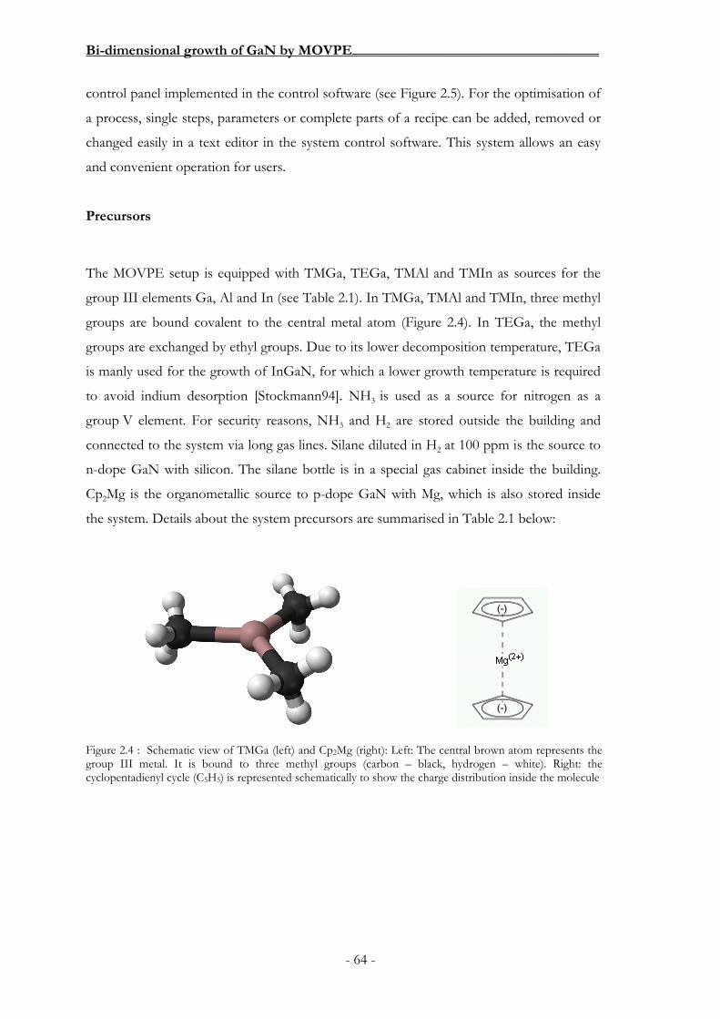
Bi-dimensional growth of GaN by MOVPE__________________________________
- 64 -
control panel implemented in the control software (see Figure 2.5). For the optimisation of
a process, single steps, parameters or complete parts of a recipe can be added, removed or
changed easily in a text editor in the system control software. This system allows an easy
and convenient operation for users.
Precursors
The MOVPE setup is equipped with TMGa, TEGa, TMAl and TMIn as sources for the
group III elements Ga, Al and In (see Table 2.1). In TMGa, TMAl and TMIn, three methyl
groups are bound covalent to the central metal atom (Figure 2.4). In TEGa, the methyl
groups are exchanged by ethyl groups. Due to its lower decomposition temperature, TEGa
is manly used for the growth of InGaN, for which a lower growth temperature is required
to avoid indium desorption [Stockmann94]. NH3 is used as a source for nitrogen as a
group V element. For security reasons, NH3 and H2 are stored outside the building and
connected to the system via long gas lines. Silane diluted in H2 at 100 ppm is the source to
n-dope GaN with silicon. The silane bottle is in a special gas cabinet inside the building.
Cp2Mg is the organometallic source to p-dope GaN with Mg, which is also stored inside
the system. Details about the system precursors are summarised in Table 2.1 below:
Figure 2.4 : Schematic view of TMGa (left) and Cp2Mg (right): Left: The central brown atom represents the group III metal. It is bound to three methyl groups (carbon – black, hydrogen – white). Right: the cyclopentadienyl cycle (C5H5) is represented schematically to show the charge distribution inside the molecule

Bi-dimensional growth of GaN by MOVPE__________________________________
- 65 -
Table 2.1 : Precursors used in the MOVPE system: Pressure at 298 K, estimation of the vapour pressure P at temperature T: Log(P)=B-A/T and melting points for organometallics
Name
Function
Chemical
formula
P at 298 K
(torr)
A B Melting
point
(°C)
Trimethylgallium (TM-Ga)
Metal organic (element-III source)
Ga(CH3)3 238 1825 8.5 -15.8
Triethylgallium (TE-Ga)
Metal organic (element-III source)
Ga(C2H5)3 4.79 2530 9.19 -82.5
Trimethylaluminium (TM-Al)
Metal organic (element-III source)
Al(CH3)3 14.2 2780 10.48 15
Trimethylindium (TM-In)
Metal organic (element-III source)
In(CH3)3 1.75 2830 9.74 88
Bis(cyclopentadienyl)magnesium
(Cp2Mg) Metal organic (p-doping)
Mg(C5 H5)2 0.05 3556 10.56 175
Ammonia
Gas (element-V source)
NH3
Silane (diluted in H2 100)
Gas (n-doping)
SiH4
Hydrogen Carrier gas H2
Nitrogen Carrier gas N2

Bi-dimensional growth of GaN by MOVPE__________________________________
- 66 -
Figu
re 2
.5 :
Sche
mat
ic o
f the
reac
tor

Bi-dimensional growth of GaN by MOVPE__________________________________
- 67 -
Chemical reactions inside the reactor
The gas stream is pointed downwards in the direction of the susceptor and is slowed down
close to the surface and establishes a boundary layer. The precursors may also react inside
this boundary layer before diffusing to the substrate surface and contribute to the growth.
Figure 2.6 shows a sketch of the chemical reactions involved in the GaN precursor
decomposition [Daulesberg08]. Two main interconnected reaction channels (noted a) and
b) in Figure 2.6) can be indentified:
a) TMGa together with NH3 form the non-stable Ga(CH3)3:NH3 reaction product,
which can react to form an amide (CH3)2GaNH2 by separation of a methane molecule and
then an oligomer ([(CH3)2GaNH]n) by further methane separation. This oligomer can
transform to GaN by separation of 2n methane molecules. This can either happen on the
sample surface or in the gas phase and contributes to the growth. In parallel, GaN clusters
can be formed with diameters between 10 and 100 nm in the gas phase [Daulesberg08].
This gas phase cluster formation is particularly important at high growth pressure (close to
atmospheric pressure). These clusters do not contribute to the growth and leave the
reactor through the exhaust line.
b) The TMGa reacts directly to MMGa (monomethygallium) by separation of two
methyl groups, which can react in two different ways: (i) MMGa can form molecule the
amides already founded in a) with a NH2 or (ii) MMGa can react with NH2, CH3 and H2 to
result GaN in the gas phase.
These complex chemical reactions can be summed up in a simple reaction equation:
Ga(CH3)3 + NH3 → GaN(sol) + 3 CH4, but this formulation hides the formation of
intermediate compounds that are important in the growth mechanisms like H2 formation,
which can have an etching behaviour on GaN.
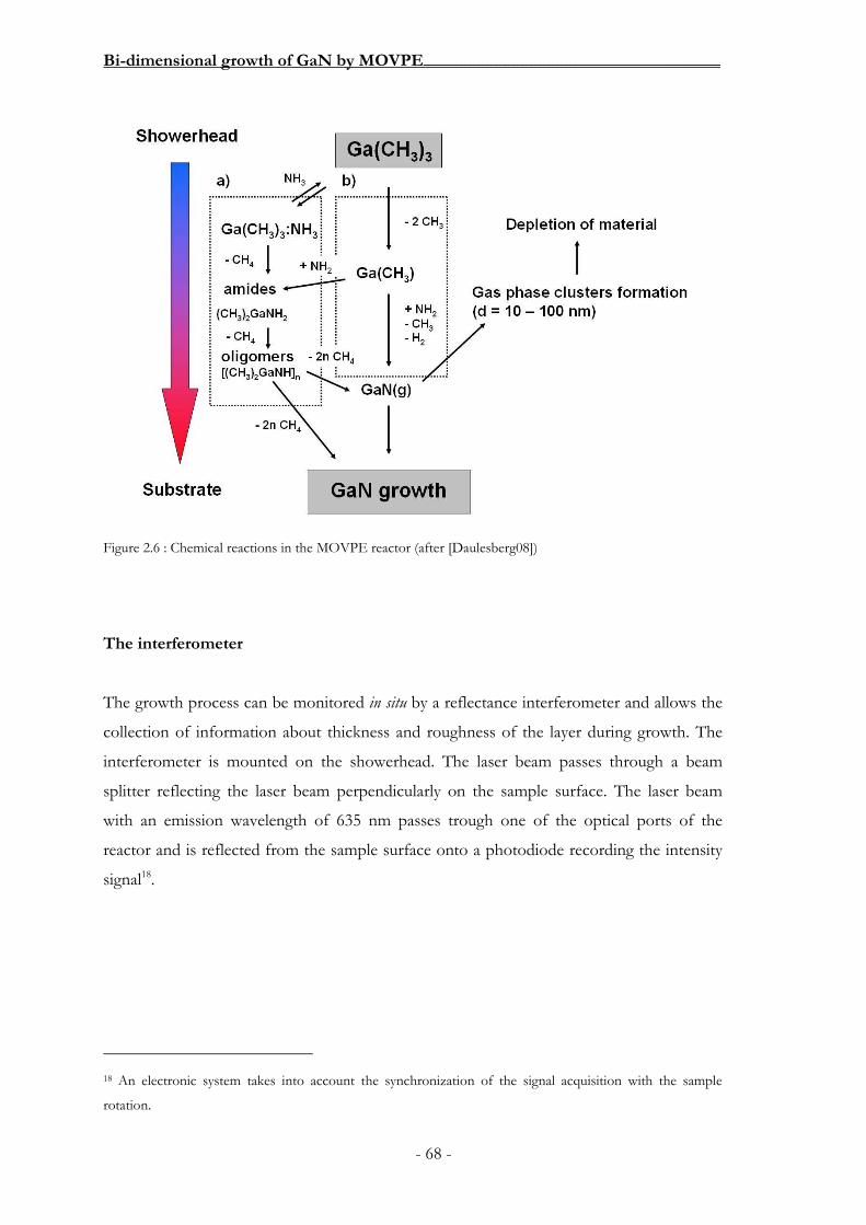
Bi-dimensional growth of GaN by MOVPE__________________________________
- 68 -
The interferometer
The growth process can be monitored in situ by a reflectance interferometer and allows the
collection of information about thickness and roughness of the layer during growth. The
interferometer is mounted on the showerhead. The laser beam passes through a beam
splitter reflecting the laser beam perpendicularly on the sample surface. The laser beam
with an emission wavelength of 635 nm passes trough one of the optical ports of the
reactor and is reflected from the sample surface onto a photodiode recording the intensity
signal18.
18 An electronic system takes into account the synchronization of the signal acquisition with the sample
rotation.
Figure 2.6 : Chemical reactions in the MOVPE reactor (after [Daulesberg08])

Bi-dimensional growth of GaN by MOVPE__________________________________
- 69 -
The incident beam undergoes two reflections; one at the air/film interface and one at the
film/substrate interface (see Figure 2.8). The reflection from the substrate bottom is
negligible since only one-side polished sapphire substrates were used here. The two
reflected beams interfere with each other leading to a total intensity changing as a function
of the film thickness and refractive index. During the film growth, the optical path
difference between the two reflections is changed leading to a periodic change of intensity
of the reflected beam. The distance between the interference maxima also depends on the
refractive index of the film and the laser wavelength.
Figure 2.7 : Diagram of the interferometer installed in top of the reactor lid (after [Webb07])
Figure 2.8 : Schematic of the light path inside the layer. The beams reflected at the air/film and film/substrate interfaces interfere with each other; phase shift depends on the thickness of the deposited film

Bi-dimensional growth of GaN by MOVPE__________________________________
- 70 -
refractive index of the film and the laser wavelength. Considering the difference of optical
path between the two beams of Figure 2.8, the grown film thickness between two maxima
is directly given by the standard formula:
nd
2
λ= (eq. 5)
where d is the film thickness, λ the probe wavelength and n the film refractive index. Using
a laser diode with 635 nm emission wavelength and a refractive index of 2.3 for GaN, the
grown layer thickness between two maxima is calculated to be 138 nm. For 2D growth, the
interferometer is absolutely crucial not only for the growth-rate estimation but also for
controlling the initial material nucleation and the roughness evolution, as will be discussed
in the section 2.3 of this chapter.
The demand of high quality and homogeneity of growth especially in industry has
lead to the development of new in situ characterisation techniques. In situ monitoring
techniques using reflectance-anisotropy spectroscopy (RAS) combined with a pyrometer
and interferometer (using polychromatic wavelength) allow the in-situ measurement of
ternary compound composition and dopant concentration in parallel with the growth rate
and the substrate-surface temperature.
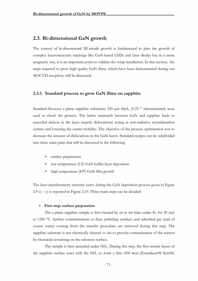
Bi-dimensional growth of GaN by MOVPE__________________________________
- 71 -
2.3. Bi-dimensional GaN growth
The control of bi-dimensional III-nitride growth is fundamental to plan the growth of
complex heterostructure stackings like GaN-based LEDs and laser diodes but in a more
pragmatic way, it is an important point to validate the setup installation. In this section, the
steps required to grow high quality GaN films, which have been demonstrated during our
MOCVD reception, will be discussed.
2.3.1. Standard process to grow GaN films on sapphire
Standard Kyocera c-plane sapphire substrates 330 µm thick, (0.25 ° misorientated) were
used to check the process. The lattice mismatch between GaN and sapphire leads to
extended defects in the layer (mainly dislocations) acting as non-radiative recombination
centres and lowering the carrier mobility. The objective of the process optimisation was to
decrease the amount of dislocations in the GaN layers. Standard recipes can be subdivided
into three main parts that will be discussed in the following:
• surface preparation
• low temperature (LT) GaN buffer layer deposition
• high temperature (HT) GaN film growth
The laser interferometry intensity curve during the GaN deposition process given in Figure
2.9 a) – e) is reported in Figure 2.10. Three main steps can be detailed:
• First step: surface preparation
The c-plane sapphire sample is first cleaned by an in situ bake under H2 for 20 min
at 1200 °C. Surface contaminations as dust, polishing residues and adsorbed gas (and of
course water) coming from the transfer procedure are removed during this step. The
sapphire substrate is not chemically cleaned ex situ to prevent contamination of the reactor
by chemicals remaining on the substrate surface.
The sample is then annealed under NH3. During this step, the first atomic layers of
the sapphire surface react with the NH3 to form a thin AlN layer [Grandjean96 Kim00,

Bi-dimensional growth of GaN by MOVPE__________________________________
- 72 -
Vennegues99, Dwikusuma03]. This AlN layer enhances the sticking of the GaN and
improves the electrical and optical properties of the forthcoming GaN film growth at high
temperature19 [Keller96].
• Second step: low temperature GaN buffer-layer deposition
A GaN nucleation buffer layer is grown during 200 s at low temperature (T = 530 °C)
and p = 600 mbar with a V/III ratio of 1980 (see Figure 2.9 a)). The enhancement of the
sticking coefficient induced by the AlN layer and the low surface mobility (also induced by
the low temperature) lead to a complete coverage of the substrate surface by a low quality
GaN layer with a high threading-dislocation density of about 1010 cm-2 [Wu96]. The
reflectivity intensity is strongly increased confirming the deposition of a 2D layer.
After this LT nucleation step, the reactor temperature is set to 1040 °C (corresponding
to the HT GaN growth temperature). This layer is then annealed under NH3 and starts to
form 3D pyramidal islands (see Figure 2.9 b)), which lead to a decrease of the laser
reflected intensity.
During the annealing, the island density is decreased (Figure 2.9 c)) because of a desorption
of materials and hydrogen etching at high temperature. The duration of this annealing step
is not fixed a priori, because it depends on the surface quality, temperature etc. and is
adjusted by the operator as a function of the reflectivity spectra evolution.
19 The importance of this AlN layer will also be stressed for wire growth in the next chapter.
Figure 2.9 : Schematics of the nucleation of GaN. a) LT GaN nucleation, b) HT annealing with island formation, c) reduction of islands by material desorption, d) HT GaN deposition: lateral and longitudinal growth of islands, e) Coalescence of islands and 2D film growth.
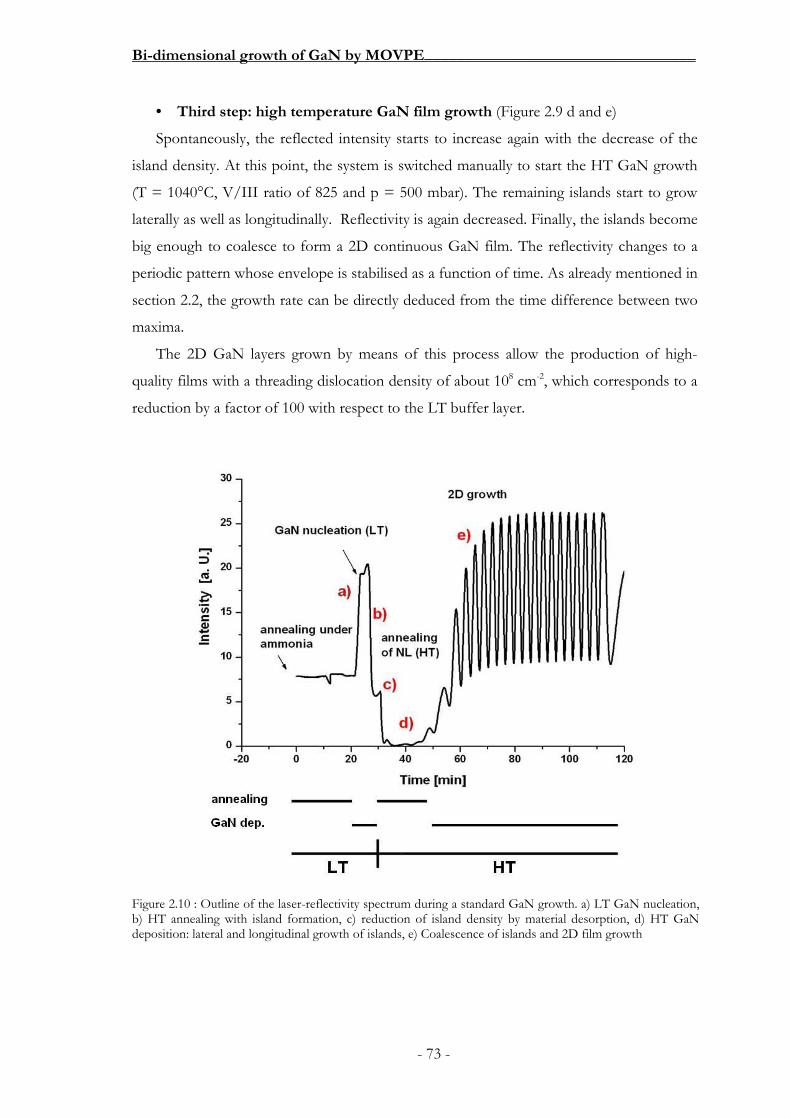
Bi-dimensional growth of GaN by MOVPE__________________________________
- 73 -
• Third step: high temperature GaN film growth (Figure 2.9 d and e)
Spontaneously, the reflected intensity starts to increase again with the decrease of the
island density. At this point, the system is switched manually to start the HT GaN growth
(T = 1040°C, V/III ratio of 825 and p = 500 mbar). The remaining islands start to grow
laterally as well as longitudinally. Reflectivity is again decreased. Finally, the islands become
big enough to coalesce to form a 2D continuous GaN film. The reflectivity changes to a
periodic pattern whose envelope is stabilised as a function of time. As already mentioned in
section 2.2, the growth rate can be directly deduced from the time difference between two
maxima.
The 2D GaN layers grown by means of this process allow the production of high-
quality films with a threading dislocation density of about 108 cm-2, which corresponds to a
reduction by a factor of 100 with respect to the LT buffer layer.
Figure 2.10 : Outline of the laser-reflectivity spectrum during a standard GaN growth. a) LT GaN nucleation, b) HT annealing with island formation, c) reduction of island density by material desorption, d) HT GaN deposition: lateral and longitudinal growth of islands, e) Coalescence of islands and 2D film growth

Bi-dimensional growth of GaN by MOVPE__________________________________
- 74 -
Morphology of GaN films
Figure 2.11 shows a cross-section scanning electron microscopy (SEM) image of undoped-
GaN/n-doped GaN grown on a c-plane sapphire. The three layers’ stacking is clearly
visible. The LT GaN buffer layer (0.45 µm) followed by a 2.9 µm thick HT u-GaN layer
can be seen above the sapphire and the structure is terminated by a 0.83 µm thick n-GaN
layer. The rough side edges, which can be seen on the picture, result from the cleaving
process.
Atomic force microscopy (AFM) measurements made on standard bi-dimensional GaN are
shown in Figure 2.12. Bi-atomic steps (seen as lines) and dislocations (dark dots) can be
observed. The TD density of the samples grown during the validation process has been
reduced to 6 x 108 cm-2. Further optimisations could decrease this value to 2 x 108 cm-2,
which is stated as the TD density for optimised processes in the literature [Amano98,
Iwaya98, Yang99a, Yang99b]. With a RMS of 0.42 nm (over 64 µm2), the flatness of the
sample is in the same order of magnitude as the flatness of the sapphire substrate
(Kyocera).
Figure 2.11 : Cross-section SEM view of a GaN stacking (low temperature, undoped and n-doped layers) grown on c-plane sapphire.
Bi-dimensional growth of GaN by MOVPE__________________________________
- 75 -
2.3.2. Doping of 2D GaN films
The doping control is an important factor for the carrier-density control in the fabrication
of LEDs and laser diodes. Unintentionally doped GaN has been measured to be n-type
with a concentration of about 3x1016 cm-3 in the present setup. Silicon and magnesium were
used as common dopants of GaN for n- and p-type respectively. Carrier concentrations of
1019 cm-3 for n-doping and 1017 cm-3 for p-doping are currently reported in the literature
[Lin93, Lee99].
n-doping
n-GaN is grown under the same growth conditions as u-GaN but at a pressure of
200 mbar and with the additional injection of silane. Silicon, a group-IV element, exhibits
one valence electron more than Ga in group III. Therefore, incorporation of Si leads to an
increase of electrons in the bulk and a decrease in electrical resistance. The carrier mobility,
function of the Si concentration, is decreased with increasing doping level [Mnatsakanov03]
and the final carrier concentration in the GaN layer directly depends on the silane molar
flow [Nakamura00]. The resistance drops quickly with increasing doping level and is
stabilised for values higher than 1 x 1018 cm-3. For the present 3x2” CCS reactor, a molar
Figure 2.12 : AFM on a bi-dimensional GaN layer obtained during the validation period of the new MOCVD setup.

Bi-dimensional growth of GaN by MOVPE__________________________________
- 76 -
flow between 1.24 nmol/min and 6.26 nmol/min leads to a doping concentration in-
between 1 x 1018 cm-3 and 5 x 1018 cm-3.
p-doping
The growth of p-GaN is more difficult than n-GaN and was first achieved in 1989
with Mg as dopant followed by low energy electron beam irradiation (LEEBI) [Amano89].
In 1992, p-GaN was obtained by a thermal annealing under N2 [Nakamura92a]. This
process, much easier to integrate in a production flow than LEEBI, favoured the very
strong development of the III-nitride devices.
p-GaN is grown at 920 °C, under a pressure of 200 mbar and a V/III ratio of 4000.
The Cp2Mg flow is 700 nmol/min. The post growth annealing is carried out at a
temperature of 750 °C in an N2 atmosphere for 20 min. During this annealing step, inactive
hydrogen-donor complexes, responsible for low doping efficiency are dissociated
[Nakamura92b, vanVechten92, Götz95]. p-GaN layers grown in the present MOVPE
system exhibit a hole concentration of 4 x 1017 cm-3 and a mobility of 9-12 V cm-2,
consistent with the values reported in the literature [Nakamura00].
The Mg incorporation in the material is very bad because less than 1% of
incorporated magnesium produces acceptor centres at room temperature due to a large
activation energy of about 200 meV [Monroy04]. Fairly large quantities of magnesium must
be incorporated to overcome the background-electron concentration due to residual
donors of the unintentional doping. It is therefore difficult to achieve a hole concentration
of 1 x 1018 cm-3 corresponding to a Mg incorporation of 1 x 1020 cm-3 because this value is
near the solubility limit for Mg [VanDeWalle98]. In contrast to Si doping, the resistance of
Mg-doped GaN increases for larger Mg content due to the increase of defects20. For all
these difficulties, the heavy p-doping of bi-dimensional GaN is often restricted to the last
5 nm of a device to avoid material damaging.
20 Moreover, the hole mobility is about a factor of 30 smaller than the electron mobility in Si-doped layers.
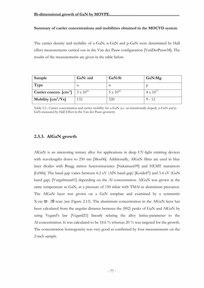
Bi-dimensional growth of GaN by MOVPE__________________________________
- 77 -
Summary of carrier concentrations and mobilities obtained in the MOCVD system
The carrier density and mobility of u-GaN; n-GaN and p-GaN were determined by Hall
effect measurements carried out in the Van der Pauw configuration [VanDerPauw58]. The
results of the measurements are given in the table below.
Sample GaN: nid GaN:Si GaN:Mg
Type u n p
Carrier concen. [cm-3] 3 x 10¹⁶ 5 x 10¹⁸ 4 x 10¹⁷
Mobility [cm2/Vs] 132 320 9 - 12
Table 2.2 : Carrier concentration and carrier mobility for u-GaN (i.e. un-intentionally doped), n-GaN and p-GaN measured by Hall Effect in the Van der Pauw geometry
2.3.3. AlGaN growth
AlGaN is an interesting ternary alloy for applications in deep UV-light emitting devices
with wavelengths down to 250 nm [Moe06]. Additionally, AlGaN films are used in blue
laser diodes with Bragg mirror heterostructures [Nakamura99] and HEMT transistors
[Li06b]. The band gap varies between 6.2 eV (AlN band gap) [Koide87] and 3.4 eV (GaN
band gap) [Vurgaftman01] depending on the Al concentration. AlGaN was grown at the
same temperature as GaN, at a pressure of 150 mbar with TMAl as aluminium precursor.
The AlGaN layer was grown on a GaN template and examined by a symmetric
X-ray ω - 2θ scan (see Figure 2.13). The aluminium concentration in the AlGaN layer has
been calculated from the angular distance between the (002) peaks of GaN and AlGaN by
using Vegard’s law [Vegard21] linearly relating the alloy lattice-parameter to the
Al-concentration. It was calculated to be 18.6 % whereas 20 % was targeted for the growth.
The concentration homogeneity was very good as confirmed by four measurements on the
2-inch sample.
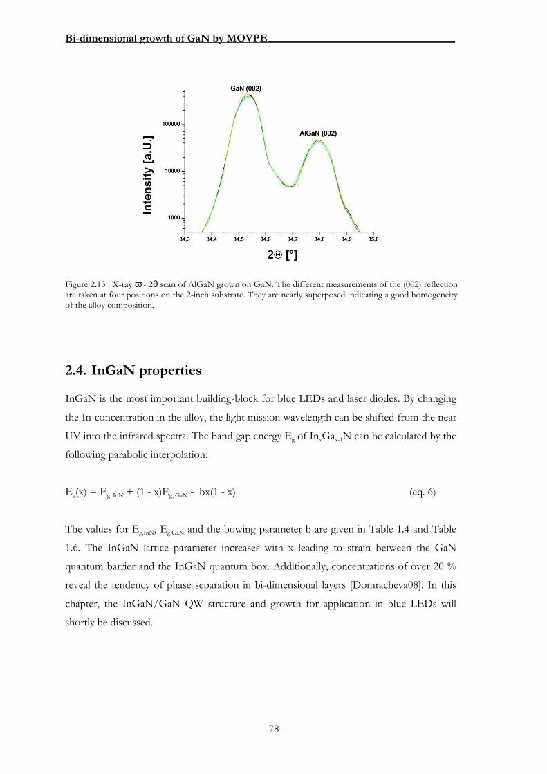
Bi-dimensional growth of GaN by MOVPE__________________________________
- 78 -
2.4. InGaN properties
InGaN is the most important building-block for blue LEDs and laser diodes. By changing
the In-concentration in the alloy, the light mission wavelength can be shifted from the near
UV into the infrared spectra. The band gap energy Eg of InxGax-1N can be calculated by the
following parabolic interpolation:
Eg(x) = Eg, InN + (1 - x)Eg, GaN - bx(1 - x) (eq. 6)
The values for Eg,InN, Eg,GaN and the bowing parameter b are given in Table 1.4 and Table
1.6. The InGaN lattice parameter increases with x leading to strain between the GaN
quantum barrier and the InGaN quantum box. Additionally, concentrations of over 20 %
reveal the tendency of phase separation in bi-dimensional layers [Domracheva08]. In this
chapter, the InGaN/GaN QW structure and growth for application in blue LEDs will
shortly be discussed.
Figure 2.13 : X-ray ω - 2θ scan of AlGaN grown on GaN. The different measurements of the (002) reflection are taken at four positions on the 2-inch substrate. They are nearly superposed indicating a good homogeneity of the alloy composition.

Bi-dimensional growth of GaN by MOVPE__________________________________
- 79 -
InGaN/GaN QW structure
As briefly discussed before, the GaN wurtzite crystal is polarised and exhibits piezoelectric
fields in the material. The origin of this spontaneous polarisation lies in the strong ionic
nature of the bond between the Ga- and the N-atoms. When the III-nitride lattice is
deformed due to external forces such as compressive or tensile stress, a piezoelectric
polarisation is induced to the crystal as a function of its orientation and the total
polarisation is the sum of the spontaneous and the piezoelectric components [Harrison05].
In InGaN/GaN QW structures grown along the c-direction, the fields have a detrimental
effect caused by the separation of the electron and hole-wave functions, a function of the
QW thickness (see Figure 2.14). This effect reduces the overlapping of the electron and
hole-wave functions decreasing the internal quantum efficiency of the structure
[Berkowicz00]. Inside a QW the electrons and the holes accumulate at opposite sides and
emission energy is smaller in comparison to the field-free case. Therefore the energy
difference between the electron- and hole-states decreases causing a red shift in the
emission spectrum of the structure. This phenomenon is known as the quantum confined
stark effect (QCSE) [Takeuchi97, Chichibu00] first observed in GaAs-AlGaAs QWs
[Chemla83].
Up to now, polarisation effects have not been of major concern in optoelectronic
devices due to the high current densities at which these components are commonly
operated (this influence will be discussed in chapter 4). Only recently, this issue has gained
more attention due to the quest towards improved internal quantum efficiency in
light-emitting devices targeted for general lighting applications.
Figure 2.14 : Schematics of the energy band in a QW without (left) and with an internal electric field (right) and illustration of the impact of the QW thickness (figures taken from [Ambacher02])

Bi-dimensional growth of GaN by MOVPE__________________________________
- 80 -
In the context of this project, a simple MQW structure composed of 5 InGaN/GaN layer
grown on a 2” c-plane sapphire substrate was studied in order to validate the control of the
growth process (see Figure 2.16).
The InGaN alloy growth is very sensitive to temperature [Kuykendall07]. The
manufacturer of this equipment empirically observed that the optical emission wavelength
of this alloy changes by about 1.5 nm per Kelvin. This means that both average
temperature and homogeneity must be controlled during the process.
In these experiments, a growth temperature of about 750 °C was chosen for the
InGaN well, the temperature variation being about 3 K on the 2” wafer. Nitrogen was used
as the carrier gas instead of hydrogen, because H2 has an etching behaviour for indium and
would reduce its incorporation into the well [Koukitu99]. The growth rate was maintained
to a low value to increase the structural quality of the layer and the typical thickness of the
quantum well was between 2 and 5 nm.
The growth of the GaN needs higher growth temperatures to achieve a good
structural quality. For the GaN barrier, a fast temperature ramping between the well and
barrier growth is important to prevent a decomposition of the InGaN well and a
compromise must be found for the barrier growth temperature: TEGa is preferred to
TMGa as a Ga source to benefit from a higher decomposition rate at a lower temperature
[Stockmann94] and the barrier growth temperature is set to about 860 °C. During the
ramping (between 750 and 860 °C), a small amount of GaN is deposited to lock the indium
in the well. The barrier is typically 10 to 15 nm thick.
Figure 2.15 : Schematic of an InGaN/GaN MQW grown on sapphire

Bi-dimensional growth of GaN by MOVPE__________________________________
- 81 -
Example of the photoluminescence measurement of a MQW
Figure 2.16 shows a superposition of five RT PL measurements of an InGaN/GaN MQW
(x 5) with a target thickness of 5 nm for the QW and 10 nm for the QB at different
positions of the sample. A He-Cd laser with an emission wavelength of 325 nm (3.82 eV)
(cut by a filter and not visible in the spectra) was used for PL excitation. The emission
peaks are centred between 442 nm (2.81 eV) and 447 nm (2.78 eV) with a FWHM of 35
nm (20 meV). The different peak positions can be explained with a difference in
temperature of ± 1.5 K at different positions of the sample. The MQW emission is about a
factor of 15 stronger than the GaN NBE emission centred at 355 nm (3.497 eV).
2.5. Integration in a simple LED structure
The building blocks demonstrated previously (2D GaN film growth, doping control and
MQW growth) have been combined in the single heterostructure shown in Figure 2.17 to
obtain a simple blue LED.
Un-intentionally doped GaN is grown on a c-plane sapphire followed by two n-
doped GaN layers: the first having a carrier concentration of 5 x 1018 cm-3 followed by a
second with a smaller carrier concentration of 1 x 1018 cm-3. The (InGaN/GaN) MQW (x
5) is grown on these layers. The use of several QWs increases the volume for electron-hole
recombination and therefore the efficiency of the LED. For a convenient carrier injection,
the QW number is usually lower than 7. The LED structure is finished by two layers of
Figure 2.16 : RT PL of an InGaN/GaN x 5 MQW: The measurements are performed at different positions on the 2-inch wafer and show a shift of the InGaN emission wavelength of about 5 nm
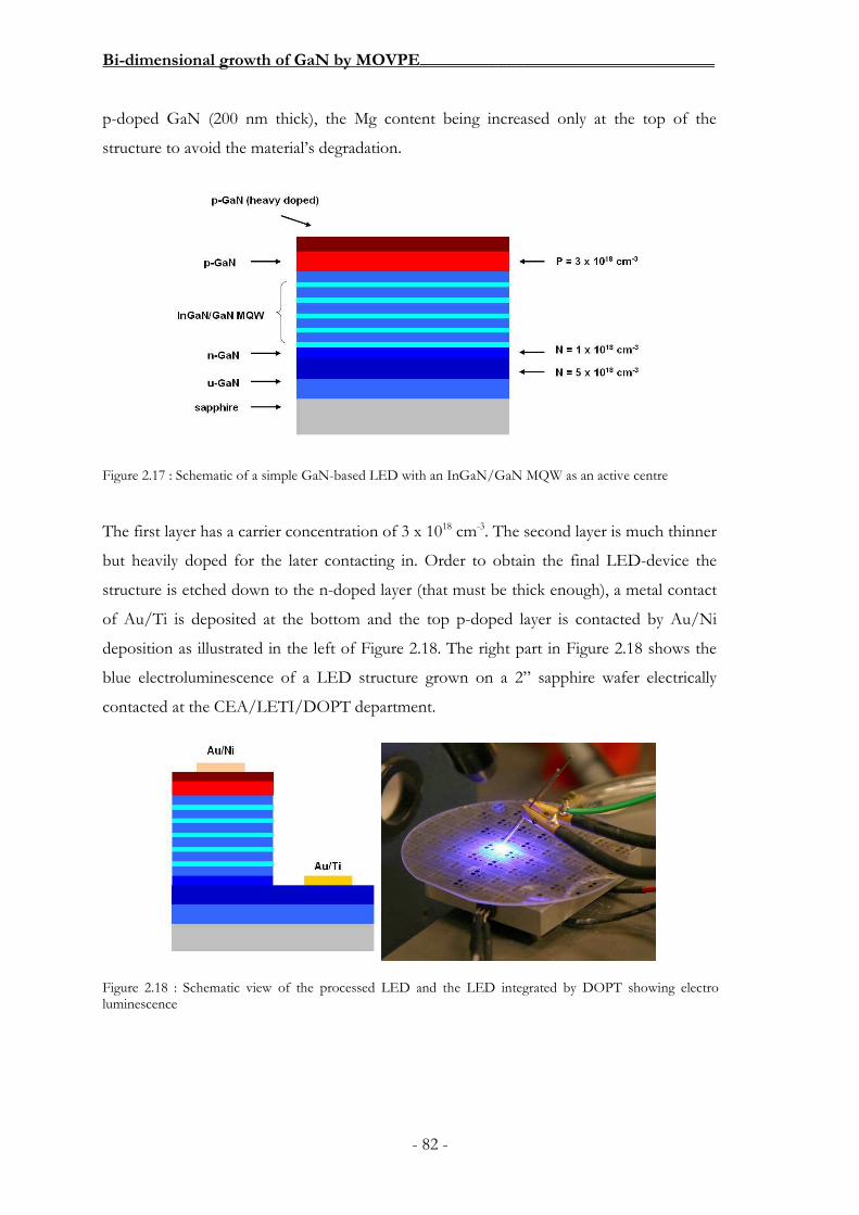
Bi-dimensional growth of GaN by MOVPE__________________________________
- 82 -
p-doped GaN (200 nm thick), the Mg content being increased only at the top of the
structure to avoid the material’s degradation.
The first layer has a carrier concentration of 3 x 1018 cm-3. The second layer is much thinner
but heavily doped for the later contacting in. Order to obtain the final LED-device the
structure is etched down to the n-doped layer (that must be thick enough), a metal contact
of Au/Ti is deposited at the bottom and the top p-doped layer is contacted by Au/Ni
deposition as illustrated in the left of Figure 2.18. The right part in Figure 2.18 shows the
blue electroluminescence of a LED structure grown on a 2” sapphire wafer electrically
contacted at the CEA/LETI/DOPT department.
Figure 2.17 : Schematic of a simple GaN-based LED with an InGaN/GaN MQW as an active centre
Figure 2.18 : Schematic view of the processed LED and the LED integrated by DOPT showing electro luminescence
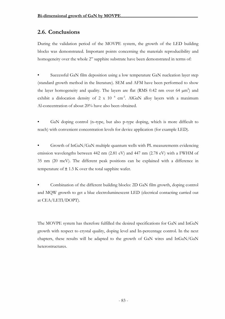
Bi-dimensional growth of GaN by MOVPE__________________________________
- 83 -
2.6. Conclusions
During the validation period of the MOVPE system, the growth of the LED building
blocks was demonstrated. Important points concerning the materials reproducibility and
homogeneity over the whole 2” sapphire substrate have been demonstrated in terms of:
• Successful GaN film deposition using a low temperature GaN nucleation layer step
(standard growth method in the literature). SEM and AFM have been performed to show
the layer homogeneity and quality. The layers are flat (RMS 0.42 nm over 64 µm2) and
exhibit a dislocation density of 2 x 10 8 cm-2. AlGaN alloy layers with a maximum
Al-concentration of about 20% have also been obtained.
• GaN doping control (n–type, but also p-type doping, which is more difficult to
reach) with convenient concentration levels for device application (for example LED).
• Growth of InGaN/GaN multiple quantum wells with PL measurements evidencing
emission wavelengths between 442 nm (2.81 eV) and 447 nm (2.78 eV) with a FWHM of
35 nm (20 meV). The different peak positions can be explained with a difference in
temperature of ± 1.5 K over the total sapphire wafer.
• Combination of the different building blocks: 2D GaN film growth, doping control
and MQW growth to get a blue electroluminescent LED (electrical contacting carried out
at CEA/LETI/DOPT).
The MOVPE system has therefore fulfilled the desired specifications for GaN and InGaN
growth with respect to crystal quality, doping level and In-percentage control. In the next
chapters, these results will be adapted to the growth of GaN wires and InGaN/GaN
heterostructures.

Bi-dimensional growth of GaN by MOVPE__________________________________
- 84 -
Chapter 3

Growth of self-assembled GaN wires_______________________________________
- 85 -
3. Growth of self-assembled GaN wires
3.1. Introduction
In the literature, MOCVD and MOVPE GaN wires are usually grown with nickel and gold
catalysts [Kuykendall03, Gottschalch08] or by catalyst-free approaches using an ex situ pre-
patterned mask [Deb05, Hersee06]. During this PhD project, an original approach has
been developed which does not require any ex situ substrate preparation before the growth.
Actually, all surface preparations are carried out in situ inside the MOCVD reactor allowing
an easier and faster growth of the wires.
The wires will be grown on a c-plane sapphire substrate as already discussed for the
growth of 2D GaN films, taking advantage of the knowledge of this well understood
process. This approach, based on in situ deposition of a thin SiNx layer (around 2 nm) on a
c-plane sapphire substrate, enables epitaxial growth of c-oriented wires with 200–1500 nm
diameters and a large length/diameter ratio (>100). The wires grow randomly on the
surface without any direct control of the seed position and have distributed diameters.
A detailed study of the growth mechanisms will show that a combination of key
parameters is necessary to promote the vertical growth, in particular the duration of the
SiNx deposition prior to the wire growth, the GaN seed-nucleation time and a high
Si-dopant concentration. This chapter will be focussed on the important steps controlling
the wire growth and the structural properties of the wires.

Growth of self-assembled GaN wires_______________________________________
- 86 -
3.2. General description of the wire growth method
Schematically, the growth of self-assembled wires can be divided into the three following
main steps
• Step I: Surface preparation
• Step II: Nucleation of GaN seeds (Carrier gas: N2, 1000 °C, V/III: 16.5,
800 mbar)
• Step III: Growth of GaN wires (with additional injection of SiH4)
All these steps will be described in detail in the following.
3.2.1. The substrate
The c-plane sapphire substrates (“Crystec - alternative supplier” with a miscut of 0.25 °)
were selected to grow the wires. As mentioned in chapter 2, GaN growth on sapphire leads
to a high defect density in 2D layers due to the strain induced by the lattice mismatch of
13.9 % between the substrate and the GaN and due to the different thermal expansion
coefficients of the materials [Ponce98]. For small wire lateral dimensions, the material is
able to relax more easily from the free surface [Raychaudhuri06, Han09, Glass06, Li09] and
the wires are less sensitive to substrate threading dislocations, which may curve at the
bottom to reach the edge surface. Figure 3.1 below shows a 1D finite element calculation
of the lateral strain without any defects. Luryi and Suhir [Li09] and Zubia, Hersee and co-
workers [Zubia99, Zubia00, Hersee02, Hersee05] were able to show in theory that in a
nanometer-scale heterojunction, the strain near the interface decays exponentially away
from the interface. This strain decay length illustrated on the right part of the figure has the
same order of magnitude as the lateral dimension of the nanojunction. Due to this
exponential strain-decay at the junction, the wire is not affected by the interfacial
lattice-mismatch strain or thermal strain, as long as the aspect ratio is greater than one.

Growth of self-assembled GaN wires_______________________________________
- 87 -
From a practical point of view, the sapphire substrate is available at a low price
(compared for example to SiC). Moreover, its transparency in the visible spectrum is
convenient for light extraction and its smaller refractive index compared to GaN explains
the general use of this substrate for LED device fabrication [Yang98].
The substrate does not have to be chemically cleaned before its introduction inside
the reactor. An annealing under hydrogen at high temperature and the nitridation
procedure described below prevent a contamination of the reactor chamber and allow a
straightforward surface preparation before the wire growth.
3.2.2. Step I: Surface preparation
The surface preparation is subdivided into four steps:
• Surface cleaning: bake of sapphire under H2 (100 mbar) during 20 min at
1050 °C
• Standard nitridation of the sapphire surface: annealing of sapphire under H2
and NH3 (1050 °C, 90 s, 100 mbar)
• SiNx deposition (1040 °C, SiH4: 200 nmol/min, NH3 : 4000 sccm, 133 mbar)
• Annealing of SiNx (1040 °C, NH 3: 4000 sccm, 133 mbar)
Figure 3.1: a) Finite element calculation of the lateral strain distribution induced by the lattice mismatch between sapphire and GaN for a wire with a diameter of 0.25 µm, b) strain along the wire (dotted line in a)) as a function of the distance between the sapphire/GaN interface for wires with different diameters [Li09]

Growth of self-assembled GaN wires_______________________________________
- 88 -
3.2.2.1. Initial treatment of the sapphire surface
The sample is baked under H2 at 1040 °C for 20 min to clean the substrate surface from
contaminations: mainly dust, adsorbed gases and water remaining from the cleaving and
transfer procedure. Additionally, due to enhanced surface diffusion, the surface topology is
smoothed by removing some polishing defaults.
AFM measurements carried out on the untreated substrate (Figure 3.3 a)) and
baked surface (Figure 3.3 b)) show a change in surface morphology induced by the bake,
especially with the formation of pits (depth of about 1 nm and diameter of several tens of
nm) with a density of about 125 pits / 100 µm2. The sapphire terraces are nevertheless still
visible on the baked surface and the flatness is maintained: the root mean square (RMS)
roughness is about 0.15 nm (over 16 µm2).
The bake is followed by an annealing step of 90 s under NH3. During this step, a
thin layer of AlN is formed on the substrate surface as already reported in the literature by
different experimental techniques (RHEED, TEM, X-ray reflectivity and X-ray
photoelectron spectroscopy) [Grandjean96, Vennegues99, Kim00, Dwikusuma03]. The
typical staircase-like surface of the sapphire is still visible in AFM indicating a very thin and
conformal layer (see Figure 3.3 c)). Even after doubling the nitridation time, the terraces
still remain visible, indicating a self-passivation of the surface, which limits the thickness of
the layer. The number of holes is increased with regard to the initial baked surface. These
Figure 3.2: The four steps of the in situ surface preparation: a) bake under H2 atmosphere, b) Surface annealing under NH3 (leading to the AlN layer formation), c) SiNx layer deposition and d) SiNx layer annealing

Growth of self-assembled GaN wires_______________________________________
- 89 -
defects can be viewed as preferential sites for the sticking of GaN during the nucleation
step.
In order to initially demonstrate the formation of an AlN layer during the annealing step,
the sample was studied by reflection high energy electron diffraction (RHEED)21. This
experiment is generally not implemented in MOCVD reactors due to the large electron
absorption induced by the working-pressure level. The samples have been transferred into
a MBE growth chamber of the laboratory under inert gas, where the measurements were
carried out. Three samples were measured by means of this technique: a) a bare sapphire,
b) an AlN layer obtained by the annealing of the sapphire during 300 s under ammonia and
c) a sapphire sample with the SiNx deposition and annealing steps (corresponding to the
complete surface preparation process). Figure 3.4 below shows the RHEED measurements
performed in the <11-20> and the <1-100> AlN azimuths for the three samples. The
diffraction strikes shown in b) demonstrate the crystalline nature of the nitridated sapphire.
The diffraction pattern corresponds to the hexagonal lattice with parameters similar to AlN
(the error bar is very large with this technique). These observations confirm the formation
of an AlN layer already discussed in the literature [Grandjean96, Vennegues99, Kim00,
Dwikusuma03]. In c), the AlN diffraction pattern became more diffuse indicating the
amorphous or nanocrystalline nature of the deposited SiNx layer. The nitridated layer signal
is still visible underneath. It can be attributed to the very thin SiNx layer thickness22 as will
be confirmed later by X-ray reflectivity experiments.
21 Courtesy to M. Azize and E. Monroy 22 An incomplete coverage can be excluded due to the results of AFM measurements.
Figure 3.3 : Initial treatment of the sapphire surface: a) untreated sapphire, b) baked sapphire, c) baked and annealed sapphire
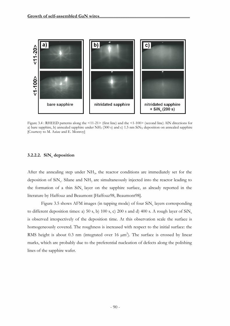
Growth of self-assembled GaN wires_______________________________________
- 90 -
3.2.2.2. SiNx deposition
After the annealing step under NH3, the reactor conditions are immediately set for the
deposition of SiNx. Silane and NH3 are simultaneously injected into the reactor leading to
the formation of a thin SiNx layer on the sapphire surface, as already reported in the
literature by Haffouz and Beaumont [Haffouz98, Beaumont98].
Figure 3.5 shows AFM images (in tapping mode) of four SiNx layers corresponding
to different deposition times: a) 50 s, b) 100 s, c) 200 s and d) 400 s. A rough layer of SiNx
is observed irrespectively of the deposition time. At this observation scale the surface is
homogeneously covered. The roughness is increased with respect to the initial surface: the
RMS height is about 0.3 nm (integrated over 16 µm2). The surface is crossed by linear
marks, which are probably due to the preferential nucleation of defects along the polishing
lines of the sapphire wafer.
Figure 3.4 : RHEED patterns along the <11-21> (first line) and the <1-100> (second line) AlN directions for a) bare sapphire, b) annealed sapphire under NH3 (300 s) and c) 1.5 nm SiNX deposition on annealed sapphire [Courtesy to M. Azize and E. Monroy]
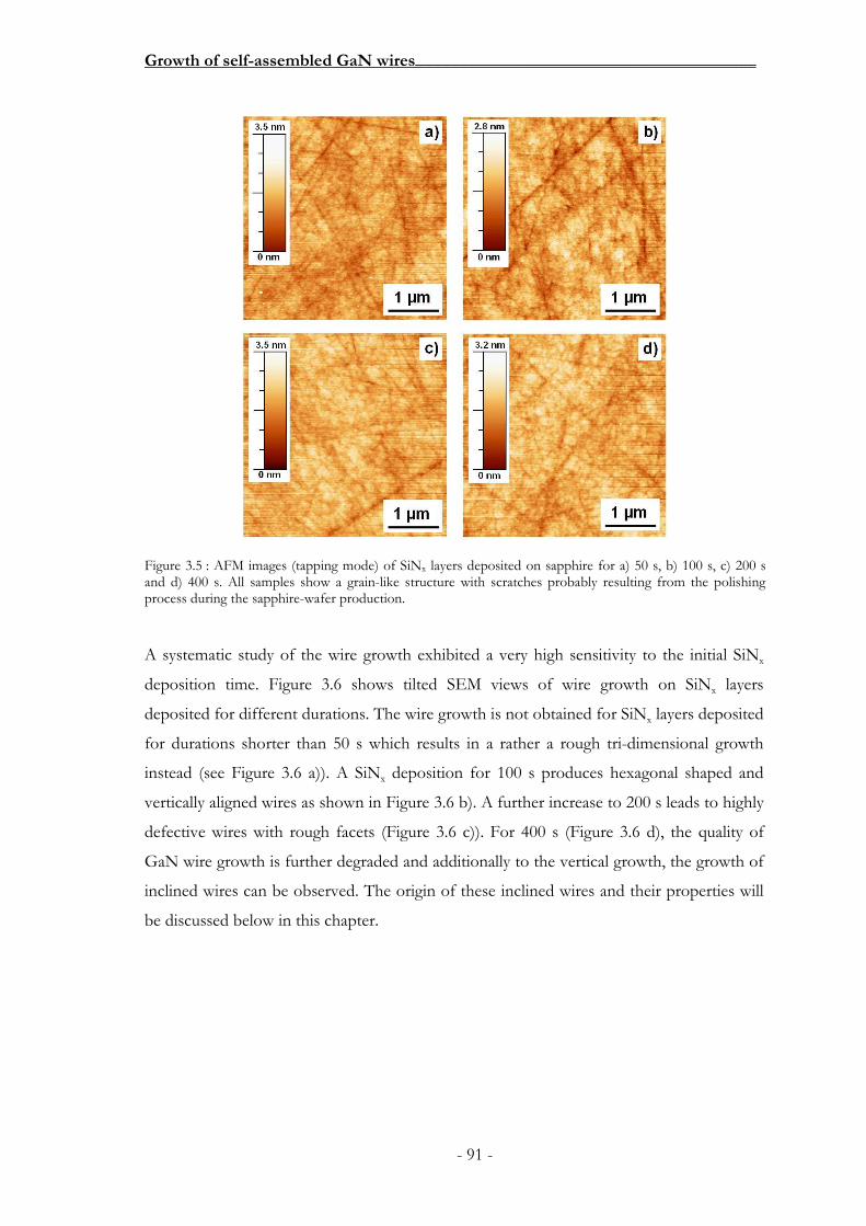
Growth of self-assembled GaN wires_______________________________________
- 91 -
A systematic study of the wire growth exhibited a very high sensitivity to the initial SiNx
deposition time. Figure 3.6 shows tilted SEM views of wire growth on SiNx layers
deposited for different durations. The wire growth is not obtained for SiNx layers deposited
for durations shorter than 50 s which results in a rather a rough tri-dimensional growth
instead (see Figure 3.6 a)). A SiNx deposition for 100 s produces hexagonal shaped and
vertically aligned wires as shown in Figure 3.6 b). A further increase to 200 s leads to highly
defective wires with rough facets (Figure 3.6 c)). For 400 s (Figure 3.6 d), the quality of
GaN wire growth is further degraded and additionally to the vertical growth, the growth of
inclined wires can be observed. The origin of these inclined wires and their properties will
be discussed below in this chapter.
Figure 3.5 : AFM images (tapping mode) of SiNx layers deposited on sapphire for a) 50 s, b) 100 s, c) 200 s and d) 400 s. All samples show a grain-like structure with scratches probably resulting from the polishing process during the sapphire-wafer production.

Growth of self-assembled GaN wires_______________________________________
- 92 -
This initial surface preparation was analysed by specular X-ray reflectivity (XRR) to provide
quantitative information on the surface electron-density in terms of layer density, thickness
and roughness of the nitridation and SiNx layers. The experiments were performed at the
European Synchrotron Radiation Facility (ESRF, Grenoble France) on the French BM32
CRG beam line at 18 keV (i.e. λ=0.069 nm). Four samples were measured: the initial
nitridated sapphire surface and the 100 s, 200 s, 800 s SiNx depositions on nitridated
sapphire.
Raw experimental curves are shown in Figure 3.7 a) as a function of the
momentum transfer Q = 4 π sinθ / λ where θ is the incidence angle. Fitted X-ray
reflectivity curves are drawn in Figure 3.7 a) and show a very good agreement with
experiments23.
23 In this analysis, the electron density profile is not a priori fixed - as is generally the case - by the
superposition of step-like or Gaussian functions the parameters of which are numerically fitted. The
drawback of this stochastic fit is to induce oscillations in the density profile which do not become visible in
simplest box/roughness models. These two approaches produce similar values of the electron density profile.
Figure 3.6 : GaN wire growth as a function of the SiNx deposition time (50 s, 100 s, 200 s and 400 s). a) 50 s: three dimensional growth; no wires are visible. b) 100 s: well aligned hexagonal shaped wires. c) 200 s: wires with a high density of structural defects. d) 400 s or longer: non vertical growth occurs additionally to the vertical growth. The insets in the pictures show details of the nucleation seeds for each deposition time.

Growth of self-assembled GaN wires_______________________________________
- 93 -
The electron density profiles normalised to the sapphire substrate are depicted in
Figure 3.7 b). It is shown that the initial nitridation step leads to a ~1.5 nm-thin layer with a
lower density than sapphire, compatible with AlN electron density. It becomes evident that
the surface roughness is quite low just after the nitridation process (see the abruptness of
the profile at the sample surface). The following SiNx deposition step increases the
thickness by about 2 nm and significantly increases the surface roughness with respect to
the initial nitridated surface. It turns out that the thickness of the SiNx layer does not
depend on the growth time. This indicates a self-passivation during deposition probably
due to the limited reaction of diluted silane with the surface. The total thickness and the
average density are slightly increased, especially for the 800 s SiNx deposition time. This
indicates that the thickness of the SiNx layer is not the most important parameter for these
wire growths but rather the roughness and density related to the chemical composition at
the surface.
3.2.2.3. Annealing of the SiNx layer
The SiNx layer is annealed under NH3 for 500 s directly after its deposition. This step is of
high importance for the later wire growth: non-annealed SiNx layers give rise to a growth
mode in which not all the wires grow perpendicularly to the surface and may be branched
from the same seed at different angles. This is called “multipod growth” and was already
Figure 3.7 : (a) X-ray reflectivity curves I/I0 of four templates before the wire growth: initial nitridated sapphire surface and 100, 200, 800 s SiNx (annealed) deposition times on nitridated sapphire. Open symbols (resp. lines) correspond to experimental (fitted) data, b) Normalised electron-density profiles with respect to sapphire density extracted from the stochastic fit with 30 slabs

Growth of self-assembled GaN wires_______________________________________
- 94 -
observed and commented in ZnO wires [Xu05, Zheng08, Lyapina08, Wang08]. Figure 3.8
shows two SEM images of a growth of GaN wires on non-annealed SiNx. Figure 3.8 a)
shows a tilted view (45°) in which several configurations of inclined wires can be identified:
1) monopod, 2) tripod and 3) bipod with an additional wire emerging perpendicularly to
the surface. Figure 3.8 b) shows a cross-section of the wire assembly viewed from the edge
of a cleaved sample. The assembly growing perpendicularly to the surface is crossed by
inclined wires with different angles.
Figure 3.9 shows plane-view SEM images demonstrating the effect of SiNx annealing on
the GaN wire growth. In Figure 3.9 a), the surface was not annealed after the SiNx
deposition and thus the surface is completely covered with multipods. Figure 3.9 b) shows
a GaN wire assembly grown on an annealed SiNx layer on which the multipod growth is
completely suppressed. The explanation of this behaviour will be discussed below in this
chapter.
Figure 3.8 : Typical multipod growth on a c-plane sapphire: a) tilted (45°) and b) cross-section view
Figure 3.9 : GaN wire growth a) without annealing under NH3: multipods are clearly visible and wires can be seen perpendicularly to the surface in the form of dots and b) with annealing under NH3: multipod growth is completely suppressed and a very small number of non-perpendicular wires can be seen.

Growth of self-assembled GaN wires_______________________________________
- 95 -
3.2.3. Step II - GaN seed nucleation for wire growth
The shape of the seeds between the wires strongly depends on the SiNx deposition time, as
shown in the insets of Figure 3.6. For 50 s of SiNx deposition, a rough GaN bi-dimensional
(2D) growth is observed indicating a coalescence of GaN (inset of Figure 3.6 a)). The GaN
nucleates as hexagonal-shaped flat seeds for 100 s, whereas six-fold pyramidal-shaped seeds
with 1101 facets occur for durations longer than 200 s (insets of Figure 3.6 b) – d))). The
seed shape appears to be critical for vertical wire growth. Indeed, only seeds with c-plane
facets permit growth of c-oriented wires in contrast to the pyramids for which tilted
growth was observed. The optimal SiNx process corresponding to the growth of well-
aligned hexagonal c-plane seeds is obtained for a SiNx layer deposited for 100 s. Vertical
wires can also emerge from the c-plane of truncated hexagonal pyramids as observed for
200 s and 400 s SiNx deposition times, but for depositions longer than 200 s, most of the
GaN seeds grow as hexagonal pyramids (without a c-plane facet) and lead to tilted wires.
The duration of the nucleation (hereafter called nucleation time) also appears as a
critical parameter to decrease the mean wire size and to improve the crystalline quality.
Figure 3.10 shows the wire growth using two different nucleation times a) 10 s and b) 100
s. The insets in Figure 3.10 show the surface morphology directly after the nucleation times
of 10 and 100 s respectively.
The mean-size of hexagonal GaN seeds is significantly reduced by decreasing the
nucleation time, which certainly explains the reduction of the wire diameter. It is clearly
Figure 3.10 : Influence of the GaN nucleation time on the wire growth. a) 10 s and b) 100 s. The growth temperature is 1000°C. The insets show the seed morphology just after the nucleation step.
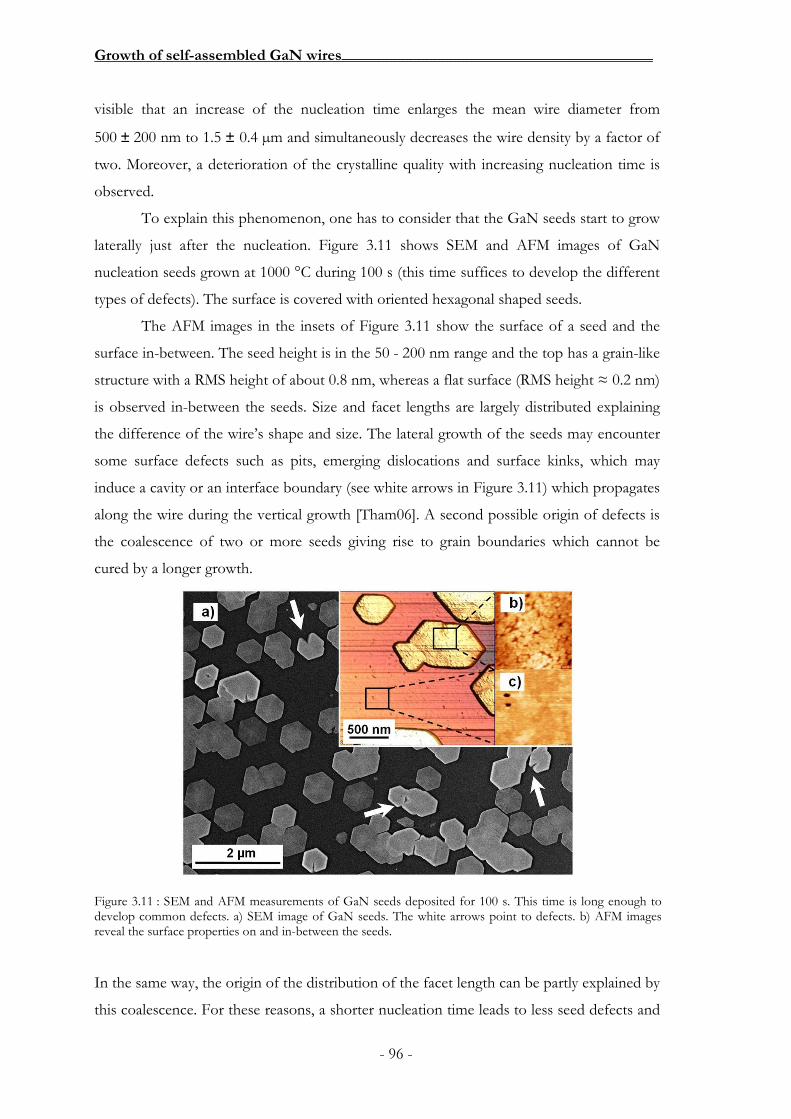
Growth of self-assembled GaN wires_______________________________________
- 96 -
visible that an increase of the nucleation time enlarges the mean wire diameter from
500 ± 200 nm to 1.5 ± 0.4 µm and simultaneously decreases the wire density by a factor of
two. Moreover, a deterioration of the crystalline quality with increasing nucleation time is
observed.
To explain this phenomenon, one has to consider that the GaN seeds start to grow
laterally just after the nucleation. Figure 3.11 shows SEM and AFM images of GaN
nucleation seeds grown at 1000 °C during 100 s (this time suffices to develop the different
types of defects). The surface is covered with oriented hexagonal shaped seeds.
The AFM images in the insets of Figure 3.11 show the surface of a seed and the
surface in-between. The seed height is in the 50 - 200 nm range and the top has a grain-like
structure with a RMS height of about 0.8 nm, whereas a flat surface (RMS height ≈ 0.2 nm)
is observed in-between the seeds. Size and facet lengths are largely distributed explaining
the difference of the wire’s shape and size. The lateral growth of the seeds may encounter
some surface defects such as pits, emerging dislocations and surface kinks, which may
induce a cavity or an interface boundary (see white arrows in Figure 3.11) which propagates
along the wire during the vertical growth [Tham06]. A second possible origin of defects is
the coalescence of two or more seeds giving rise to grain boundaries which cannot be
cured by a longer growth.
In the same way, the origin of the distribution of the facet length can be partly explained by
this coalescence. For these reasons, a shorter nucleation time leads to less seed defects and
Figure 3.11 : SEM and AFM measurements of GaN seeds deposited for 100 s. This time is long enough to develop common defects. a) SEM image of GaN seeds. The white arrows point to defects. b) AFM images reveal the surface properties on and in-between the seeds.

Growth of self-assembled GaN wires_______________________________________
- 97 -
consequently to better structural quality of the wire assembly. The optimal nucleation time
is about 10 s to minimise the quantity of structural defects.
3.2.4. Step III: Growth of GaN wires
In the following the important process parameters to control the GaN wire growth:
temperature, V/III ratio, carrier gas and precursor flows will be discussed. Moreover, the
importance of silane injection in driving the vertical growth will be stressed. To simplify the
presentation, the following parameters have been varied independently while keeping the
others fixed:
• V/III ratio
• Silane injection
• Temperature
• Wire growth time
• Carrier-gas flow
• Precursor-flow rate
• Substrate miscut
This will allow some general conclusions about the growth mechanisms of the GaN wires,
but it will also stress the complexity of the MOVPE growth technique.
3.2.4.1. V/III ratio
The V/III ratio corresponds to the molar ratio of group III (Ga) and group V (N)
precursor flow. As already discussed in chapter 2, bi-dimensional GaN is grown with a
V/III ratio around ~1000. For the one-dimensional wire growth, the V/III ratio must be
decreased to about 16 to optimize the structural and optical properties (see chapter 4).
Experiments have shown that switching to a high V/III ratio during the wire
growth immediately leads to strong lateral growth. This increase of the V/III ratio during
the growth can be used to coalesce the upper part of a wire assembly in order to facilitate
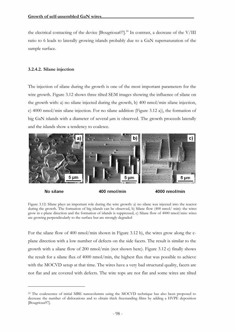
Growth of self-assembled GaN wires_______________________________________
- 98 -
the electrical contacting of the device [Bougrioua07].24 In contrast, a decrease of the V/III
ratio to 6 leads to laterally growing islands probably due to a GaN supersaturation of the
sample surface.
3.2.4.2. Silane injection
The injection of silane during the growth is one of the most important parameters for the
wire growth. Figure 3.12 shows three tilted SEM images showing the influence of silane on
the growth with: a) no silane injected during the growth, b) 400 nmol/min silane injection,
c) 4000 nmol/min silane injection. For no silane addition (Figure 3.12 a)), the formation of
big GaN islands with a diameter of several µm is observed. The growth proceeds laterally
and the islands show a tendency to coalesce.
For the silane flow of 400 nmol/min shown in Figure 3.12 b), the wires grow along the c-
plane direction with a low number of defects on the side facets. The result is similar to the
growth with a silane flow of 200 nmol/min (not shown here). Figure 3.12 c) finally shows
the result for a silane flux of 4000 nmol/min, the highest flux that was possible to achieve
with the MOCVD setup at that time. The wires have a very bad structural quality, facets are
not flat and are covered with defects. The wire tops are not flat and some wires are tilted
24 The coalescence of initial MBE nanocolumns using the MOCVD technique has also been proposed to decrease the number of dislocations and to obtain thick freestanding films by adding a HVPE deposition [Bougrioua97].
Figure 3.12: Silane plays an important role during the wire growth: a) no silane was injected into the reactor during the growth. The formation of big islands can be observed, b) Silane flow (400 nmol/ min): the wires grow in c-plane direction and the formation of islands is suppressed, c) Silane flow of 4000 nmol/min: wires are growing perpendicularly to the surface but are strongly degraded

Growth of self-assembled GaN wires_______________________________________
- 99 -
with respect to the substrate surface. Due to the high amount of defects, some wires stop
growing, others show the tendency to coalesce.
The use of silane to favour the vertical growth has already been reported in the
literature [Haffouz98]. Density-functional theory calculations have predicted that a
Ga-polar c-plane surface is formed by a Ga bilayer with Si incorporated underneath under
Ga-rich condition silane injection [Rosa06] and a catalytic role of this bi-layer can be
suspected.
However, the impact of the Si incorporation under silane flow remains inexplicable
at this point due to the lack of insights into the atomic configuration of the wire sides
(e.g. m-plane) and the diffusion barriers on the present surface.
For very high silane flow (as observed with several thousands of nmol/min), it can
be assumed that the high silicon content (> 1020 cm-3) incorporated in the material leads to
a high density of crystalline defects, which may prevent the growth of regular wires.
Further experiments showed that the silane source can be turned off after the wires
have reached a length of about 5 µm. Why this continuation of growth without silane is
possible and what mechanisms are involved, are presently open questions requiring deeper
investigations.
3.2.4.3. Temperature
The reactor temperature is a fundamental parameter governing the process of chemical
reactions. The reaction rates of the basic MOCVD mechanisms given in chapter 2 and the
surface diffusion rates are strongly temperature dependent, both variables having a strong
influence on the seed nucleation and the wire growth.
To evaluate the overall impact of the temperature on the applied technique, the
reactor temperature was decreased in a first series of experiments by several tens of degrees
during the nucleation and growth steps. Figure 3.13 compares a nucleation and growth
carried out at 1000 °C and 970 °C, the other parameters being kept identical. In spite of the
small temperature difference of 30 °C, a strong decrease in structural quality is observed
(see the wire facets) and the wire diameter in b) is decreased by a factor two compared to
a). Additionally, an increase of density by a factor five becomes evident. This strong
influence of the temperature can probably be explained by a decrease of the surface

Growth of self-assembled GaN wires_______________________________________
- 100 -
diffusion length at a lower temperature leading to both a decrease of the seed diameter and
an increase of the seed density.
A decrease of temperature goes along with an increase of the deposition rate. The
quantity of pre-reactions in the gas phase is reduced allowing more materials to reach the
surface. This increase of deposition with a decreased surface-diffusion length impedes a
proper crystal formation. Additionally, a higher seed density raises the risk of coalescence
of two or more seeds, which also leads to the formation of defects.
In a second series of experiments, the temperature was stepwise decreased from 1000 °C to
800 °C during the wire growth for a given nucleation step. In this case, the temperature
influence during the growth is decoupled from the seed nucleation step.
The growth temperature starting at 1000 °C was decreased in 50 °C steps down to
800 °C. At each temperature, GaN was deposited during 250 s and no precursors were
injected into the reactor during the temperature ramping of 75 s. Figure 3.14 shows a SEM
image of the resulting growth. The bottom part, grown at 1000 °C, shows the expected
wire geometry: the side facets are smooth with a low defect density as in standard growth.
With decreasing temperature, the material quality starts to deteriorate and forms foam-like
Figure 3.13 : Influence of nucleation and growth temperature (equal in these experiments) on wire density, diameter and structural quality for two temperatures: a) 1000 °C and b) 970 °C. The structural quality is decreased while the density is multiplied by a factor five.
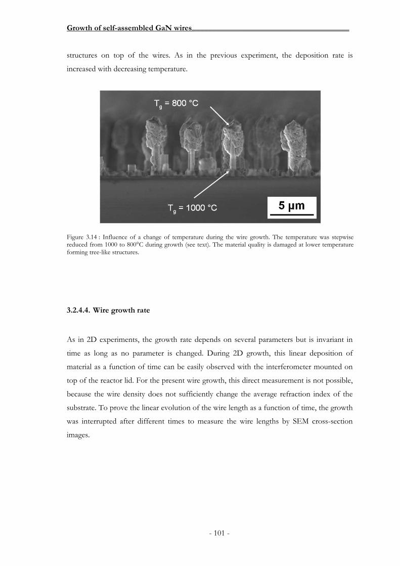
Growth of self-assembled GaN wires_______________________________________
- 101 -
structures on top of the wires. As in the previous experiment, the deposition rate is
increased with decreasing temperature.
3.2.4.4. Wire growth rate
As in 2D experiments, the growth rate depends on several parameters but is invariant in
time as long as no parameter is changed. During 2D growth, this linear deposition of
material as a function of time can be easily observed with the interferometer mounted on
top of the reactor lid. For the present wire growth, this direct measurement is not possible,
because the wire density does not sufficiently change the average refraction index of the
substrate. To prove the linear evolution of the wire length as a function of time, the growth
was interrupted after different times to measure the wire lengths by SEM cross-section
images.
Figure 3.14 : Influence of a change of temperature during the wire growth. The temperature was stepwise reduced from 1000 to 800°C during growth (see text). The material quality is damaged at lower temperature forming tree-like structures.
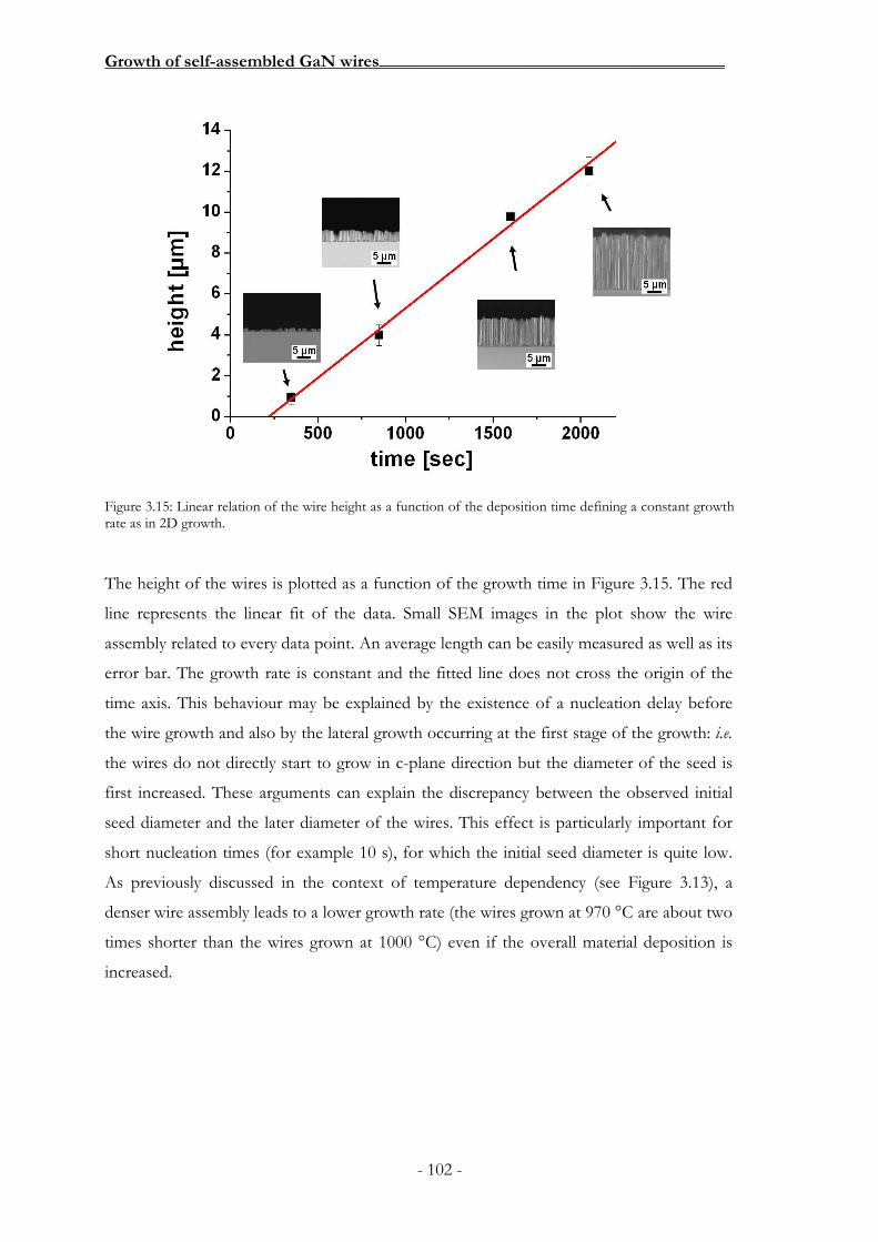
Growth of self-assembled GaN wires_______________________________________
- 102 -
The height of the wires is plotted as a function of the growth time in Figure 3.15. The red
line represents the linear fit of the data. Small SEM images in the plot show the wire
assembly related to every data point. An average length can be easily measured as well as its
error bar. The growth rate is constant and the fitted line does not cross the origin of the
time axis. This behaviour may be explained by the existence of a nucleation delay before
the wire growth and also by the lateral growth occurring at the first stage of the growth: i.e.
the wires do not directly start to grow in c-plane direction but the diameter of the seed is
first increased. These arguments can explain the discrepancy between the observed initial
seed diameter and the later diameter of the wires. This effect is particularly important for
short nucleation times (for example 10 s), for which the initial seed diameter is quite low.
As previously discussed in the context of temperature dependency (see Figure 3.13), a
denser wire assembly leads to a lower growth rate (the wires grown at 970 °C are about two
times shorter than the wires grown at 1000 °C) even if the overall material deposition is
increased.
Figure 3.15: Linear relation of the wire height as a function of the deposition time defining a constant growth rate as in 2D growth.

Growth of self-assembled GaN wires_______________________________________
- 103 -
3.2.4.5. Carrier gas flow
The carrier-gas flow transports the precursors through the MO and hydrate lines into the
reactor chamber. Its influence on the wire growth can be demonstrated using two different
carrier gas flow rates. Figure 3. shows two cross-section view SEM images with a)
4000 sccm N2 and b) 1000 sccm N2 in the MO and hydrate line respectively. The growth
rates are estimated respectively to 30 µm/h and 140 µm/h.
This increase in growth rate can be explained by the change of the precursor’s dwell
time and dilution inside the reactor chamber. The lower the carrier gas flow rate, the longer
the precursors remain in the reactor chamber and contribute to the wire growth. In parallel,
the precursors are less diluted, which increases the gas phase reaction rate. Figure 3. b) also
contains some wires which stop to grow at a very early stage. All these wires exhibit a top
facet which is not c-plane preventing the vertical growth. Simultaneously, the wires increase
their diameters with increasing length. This effect can be observed in Figure 3. b) by
comparing the bottom part of the wires with the top part. This effect however only occurs
for wires with a length of several tens of µm. The origin of this very original increase of the
lateral growth is not well understood but could be attributed to a gradient between the
wire’s temperature and the temperature of the surrounding gas. The GaN wire with its high
heat conductivity probably exhibits the same temperature as the substrate (with reference
to the calculations of [Glas06b]), whereas the gas phase is cooler due to the vertical gas
stream in the reactor and the lower heat conductivity of the gases.
The wire shape featuring an increasing diameter with increasing length is of great
importance in the attempt to establish a comparison between MOCVD mechanisms and
MBE mechanisms. In MBE, the material’s diffusion on the surface and on the wire edges
(see Figure 3.16 ) may result in a cone shape with the exact opposite gradient in diameter
and it may be concluded that these diffusion contributions are therefore not so important
in our growth. The lengths of the wires are also significantly different, i.e. much longer, for
MOCVD. With MBE, it is quite easy to reach the limit of the species diffusion at a given
temperature but a saturation value of the length as a function of time was never reached.
Further experiments with longer growth times will be necessary.
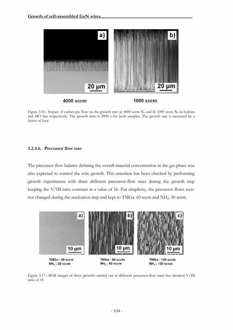
Growth of self-assembled GaN wires_______________________________________
- 104 -
3.2.4.6. Precursor flow rate
The precursor flow balance defining the overall material concentration in the gas phase was
also expected to control the wire growth. This assertion has been checked by performing
growth experiments with three different precursor-flow rates during the growth step
keeping the V/III ratio constant at a value of 16. For simplicity, the precursor flows were
not changed during the nucleation step and kept to TMGa: 60 sccm and NH3: 50 sccm.
Figure 3.16 : Impact of carrier-gas flow on the growth rate: a) 4000 sccm N2 and b) 1000 sccm N2 in hydrate and MO line respectively. The growth time is 2000 s for both samples. The growth rate is increased by a factor of four.
Figure 3.17 : SEM images of three growths carried out at different precursor-flow rates but identical V/III ratio of 16

Growth of self-assembled GaN wires_______________________________________
- 105 -
Figure 3.17 shows SEM images of wire growths for the following wire-growth conditions:
a) TMGa: 30 sccm, NH3: 25 sccm, b) TMGa: 60 sccm, NH3: 50 sccm (standard precursor
flows) and c) TMGa: 120 sccm, NH3: 100 sccm. During the growth, the N2 carrier-gas flow
was set to 1000 sccm both in the MO and Hydrate-lines. The growth times were 500 s. In
case of the lowest precursor flow a), the surface is covered with seeds formed during the
nucleation step and no wire growth is observed. The next higher flow rate b) corresponds
to our reference standard giving acceptable wires and doubling the precursor flow in c)
leads to an increase of the wire’s assembly density compared to b) in parallel with a
decrease in length. In agreement with the previous discussions, the distribution becomes
broader and wires with a diameter of several µm can be observed.
In the case of a low precursor flow rate of a), most of the material is consumed
during the pre-reaction in the gas phase and leaves the reactor chamber through the
exhaust. The material-desorption rate is higher than the deposition rate and no wires can be
grown.
The explanation of the difference between image b) and c) is more difficult to find.
Of course, a higher precursor gas phase concentration leads to a higher material deposition
and therefore to a higher wire density. But up to now, it is not understood why the wire’s
diameter distribution becomes larger and how this influences the growth.
3.2.4.7. Substrate miscut
In 2D GaN growth, a relatively low (~0.1 °) substrate miscut leads to a significantly
rougher surface as already reported in the literature [Lu04]. To test the influence of the
substrate, self-assembled GaN wire growths were carried out on different c-plane sapphire
substrates in the same run. Figure 3.18 shows SEM images for growths on a) a Crystec
alternative supplier substrate with a miscut of 0.25 ° and b) a Kyocera substrate with a
miscut of less than 0.1 °. The wire density in a) is much higher compared to that in b). On
the Kyocera substrates, the wires are generally larger and less dense. It shows that this self-
organised method is sensitive to the substrate features in particular to the miscut, which
may change the formation of the thin SiNx layer and may drive the seed nucleation. This
interpretation is also reinforced by the fact that pyramidal shaped seeds are measured in-
between the wires in b) as opposed to a).

Growth of self-assembled GaN wires_______________________________________
- 106 -
3.3. Structural characterisation of GaN wires
3.3.1. Epitaxial relationships
In order to determine the epitaxial relationship of the wires with respect to the substrate,
the usual scan along the [0 0 L] direction of the sapphire in the standard θ−2θ geometry
was first performed as a reference of a typical wire growth. Figure 3.19 shows that this scan
can be indexed with the (0 0 6) and (0 0 12) α-Al2O3 Bragg reflections ( cR3 , c = 1.299
nm) and the (0 0 2) and (0 0 4) wurtzite GaN Bragg reflections (P63mc, c = 0.5188 Å)
indicating a growth along the c-axis.
Figure 3.18 : Wire growth on a) Crystec – alternative supplier substrate (miscut 0,25°) and b) Kyocera substrate (miscut < 0,1°)
Figure 3.19 : Scan along the [0 0 L] direction of the sapphire substrate of a sample with GaN wires (standard Θ-2Θ geometry). Experiments were performed at ESRF with a wavelength of λ=0.06888 nm. GaN and sapphire indexations are in agreement with the usual bulk lattice parameters.

Growth of self-assembled GaN wires_______________________________________
- 107 -
Grazing incidence (αi) and emergence angles close to the critical angle of total reflection
allow measurements of the diffraction of planes perpendicular to the surface for the
sapphire substrate and the wires, as well as possible 2D or 3D substrate overgrowths. The
beam footprint on the sample surface, which is about 10 x 0.5 mm2, integrates the
intensities of a very large number of wires. These wire growths exhibit quite narrow
orientation distributions, which allow studying the wire’s reciprocal space according to the
substrate lattice [Eymery07]. Consider, as a reference, the conventional hexagonal c-plane
sapphire surface unit cell (a = 0.4758 nm, c = 1.2991 nm), which is defined by (H K L)
Miller indices. Radial scans along the (H 0 0) and (H H 0) sapphire in-plane Bragg
reflections are shown in Figure 3.20 a) and b). For a small grazing incidence (αi = 0.05°),
only surface contributions are measured, whereas the substrate peaks can be recorded for
αi = 0.3°. The peak indexation shows that along the (H H 0)Sap. (resp. (H 0 0)Sap.) scans, the
(H 0 0)GaN (resp. (H H 0)GaN) peaks can be measured, confirming the conventional 30°
rotation around the c-axis between the two unit cells, i.e. [ ]0011 GaN // [ ]1021 Al2O3 and
[ ]0001GaN // [ ]0001Al2O3. This measurement is also in agreement with Figure 3.11 in which
the wire seeds were oriented in the same direction.
Figure 3.20 : X-ray diffraction measurements of GaN wires grown on c-sapphire. (a-b) In-plane grazing incidence X-ray diffraction measurements at two incidence angles (αi=0.05, 0.3°) along the (a) [H 0 0] Sap. (resp. (b) [H H 0] Sap.) sapphire directions and corresponding to [H 0 0] GaN (resp. [H H 0] GaN) GaN lattice. (c-d) (0 1 L) and (0 2 L) crystal truncation rod.

Growth of self-assembled GaN wires_______________________________________
- 108 -
The plane stacking along the wire c-axis can be analysed by means of the Crystal
Truncation Rod (CTR) measurements [Feidenhans89]. The (0 1 L)GaN CTR is measured for
two grazing incidence angles (αi= 0.05, 0.4°) in Figure 3.20 c). The three main peaks can be
assigned to GaN (see the indexation given in the figure) and their positions are consistent
with the bulk GaN parameters: for example, the third peak at L3 = 7.528 in the sapphire
reciprocal units corresponds to L = L3 × 0.5188 / 1.2991 = 3.006 in the GaN reciprocal
lattice units. It shows an almost complete relaxation emphasising the small influence of the
sapphire/interfacial layer substrate strain as expected for wire geometry and the limited
impact of Si incorporation on the lattice parameter. Moreover, these peaks reveal the wire
characteristic features [Eymery07]: the intensity is not sensitive to αi and a splitting of the
peaks can be observed as a function of αi for an improved instrumental resolution (not
shown here). Due to symmetry considerations, hexagonal variants obtained by 60° in-plane
rotations (see the notation shown in Figure 3.20 c) and d)) are present in equal
proportions in the sample as confirmed by the measurements of the (0 2 L)GaN CTR.
Stacking defects along the c-plane direction give rise to a local cubic structure, which may
be measured by means of CTRs. The (0 1 L) GaN CTRs show few stacking faults in the
sample (see the small intensity peaks in Figure 3.20 c)), but they are not visible in the
(0 2 L) CTR measured at another footprint position indicating a lateral heterogeneity.
Moreover, these defect peaks can not be unambiguously attributed to the wires; they may
also stem from the substrate overgrowth and further experiments are necessary to solve
this point.
To further analywe the epitaxy, the twist and tilt of the wire assembly was
measured. The twist is directly estimated from a rotation around the surface normal (∆ω-
scan) of in-plane reflections. Figure 3.20 e) shows the results for the (3 0 0), (6 0 0) and (9 0
0) peaks. Assuming a Gaussian peak shape, the FWHM corresponds to a 0.342 ± 0.015°
twist angle. This result is significantly lower than the twist values obtained by MBE
epitaxial growth of GaN wires on Si substrate [Songmuang07, Horak08] in spite of the
growth through the thin silicon nitride layer openings.
The tilt is measured using typical rocking curves (∆θ-scan) for (0 0 L) peaks using
the Williamson–Hall plot [Cierchia03]. The GaN scans shown in Figure 3.20 f) for L = 2,
4, 6 gives a straight estimation of the wire tilt angle 0.61 ± 0.01° from the slope of the
linear plot of the FWHM of the rocking curve as a function of the reflection order.

Growth of self-assembled GaN wires_______________________________________
- 109 -
3.3.2. STEM studies on single wires
To gain a better understanding of the structural properties of the wires, scanning
transmission electron microscopy (STEM) experiments were performed on single wires as
shown in Figure 3.21. Convergent beam electron diffraction (CBED) measurements also
revealed the existence of N-polar as well as Ga-polar side crystals on single wires. The N-
and Ga-polar crystals are denoted by N and Ga respectively.
From our MOVPE experiments, it seems that Ga-polar wire crystals are usually less stable
than N-polar ones and show the tendency to develop non-c-plane facets at the top of the
wires (visible in all three images, especially in Figure 3.21 a)). This observation may imply
explanation for the change of facet orientation during the growth and thus the abrupt stop
of wire growth. The origin of the formation of different polarities during wire growth is
presently under study (PhD thesis of G. Perillat-Merceroz) and will be compared with
polarity orientations in other systems, particularly in ZnO nanowires.
Figure 3.21: STEM images of single GaN wires. CBED measurements (not shown here) reveal N-polar as well as Ga-polar crystals.

Growth of self-assembled GaN wires_______________________________________
- 110 -
3.4. Seeds morphology and wire orientation
In section 3.2.3, the influence of the seed nucleation on the wire growth was discussed and
it could be shown that the diameter and the structural quality were strongly related to this
step. It also became evident that GaN nucleation on a non-annealed SiNx mask gave rise to
the growth of multipods. The multipod growth is a parasitic wire growth occurring in
competition with the standard c-direction wire growth. Multipods may be prevented by an
annealing under NH3 directly after the SiNx deposition. This type of growth has been
mentioned for ZnO wires several times in the literature [Wang04b, Chen04, Xu05,
Zheng08, Wang08, Feng09, Hongsith09] and occurs both, in the catalyst and catalyst-free
approaches. For catalyst-driven growth of ZnO, the multipods exhibit complex
configurations, in which the numbers of branches and the spatial orientations are not well
defined. Hedgehog-like shapes can be observed. In contrast, the catalyst-free approach
gives rise to tripods, tetrapods and hexapods with highly symmetrical configurations
resulting from multi-facet nucleation centres.
For MOVPE GaN wires, the multipod wires are tilted with respect to the c-plane
growth direction and have their origin in surface seeds. Even if this type of growth is not
desirable, its study gives valuable information about the understanding of the nucleation
seeds necessary for the wire growth. As demonstrated in Figure 3.6, the seed shape changes
from a flat hexagonal shape to hexagonal shaped pyramids for SiNx deposition times of 200
s or longer. In a deeper analysis of Figure 3.9 a) and Figure 3.23, a six-fold symmetry is
visible in the multipod growth indicating an epitaxial relationship with the substrate. The
origin of this six-fold symmetry can be found in the hexagonal shaped pyramids shown in
Figure 3.6 c) and d), which will be studied in the following.
3.4.1. Experimental conditions for multipod growth
To test the assumption that hexagonal shaped pyramids give rise to the multipods, a
growth on non-annealed SiNx was interrupted at a very early stage, i.e. after 400 seconds in
order to still be able to identify the seeds, and then observed by SEM. In Figure 3.22, four
early stage multipods are imaged: a) shows the very beginning of a single tilted wire
(monopod), b) the rise of a tripod and c) and d) the beginning of a bipod growth. It is
clearly visible that the multipods grow from the pyramidal-shaped seed facets, similar to the
catalyst free approach of ZnO growth. At their early growth stage, the wires are still
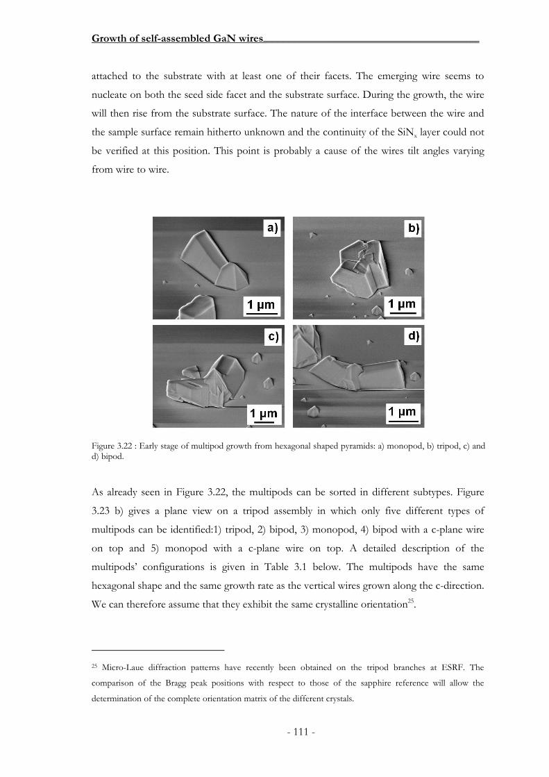
Growth of self-assembled GaN wires_______________________________________
- 111 -
attached to the substrate with at least one of their facets. The emerging wire seems to
nucleate on both the seed side facet and the substrate surface. During the growth, the wire
will then rise from the substrate surface. The nature of the interface between the wire and
the sample surface remain hitherto unknown and the continuity of the SiNx layer could not
be verified at this position. This point is probably a cause of the wires tilt angles varying
from wire to wire.
As already seen in Figure 3.22, the multipods can be sorted in different subtypes. Figure
3.23 b) gives a plane view on a tripod assembly in which only five different types of
multipods can be identified:1) tripod, 2) bipod, 3) monopod, 4) bipod with a c-plane wire
on top and 5) monopod with a c-plane wire on top. A detailed description of the
multipods’ configurations is given in Table 3.1 below. The multipods have the same
hexagonal shape and the same growth rate as the vertical wires grown along the c-direction.
We can therefore assume that they exhibit the same crystalline orientation25.
25 Micro-Laue diffraction patterns have recently been obtained on the tripod branches at ESRF. The
comparison of the Bragg peak positions with respect to those of the sapphire reference will allow the
determination of the complete orientation matrix of the different crystals.
Figure 3.22 : Early stage of multipod growth from hexagonal shaped pyramids: a) monopod, b) tripod, c) and d) bipod.
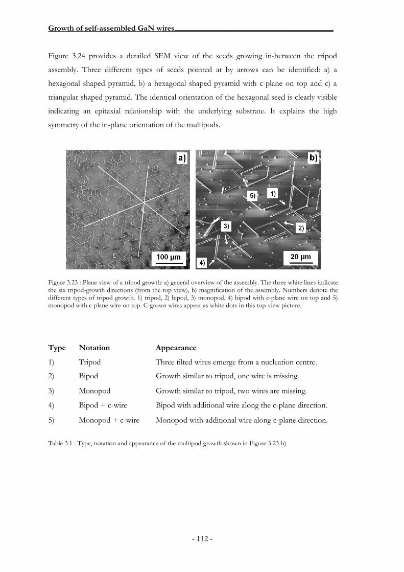
Growth of self-assembled GaN wires_______________________________________
- 112 -
Figure 3.24 provides a detailed SEM view of the seeds growing in-between the tripod
assembly. Three different types of seeds pointed at by arrows can be identified: a) a
hexagonal shaped pyramid, b) a hexagonal shaped pyramid with c-plane on top and c) a
triangular shaped pyramid. The identical orientation of the hexagonal seed is clearly visible
indicating an epitaxial relationship with the underlying substrate. It explains the high
symmetry of the in-plane orientation of the multipods.
Table 3.1 : Type, notation and appearance of the multipod growth shown in Figure 3.23 b)
Figure 3.23 : Plane view of a tripod growth: a) general overview of the assembly. The three white lines indicate the six tripod-growth directions (from the top view), b) magnification of the assembly. Numbers denote the different types of tripod growth. 1) tripod, 2) bipod, 3) monopod, 4) bipod with c-plane wire on top and 5) monopod with c-plane wire on top. C-grown wires appear as white dots in this top-view picture.
Type Notation Appearance
1) Tripod Three tilted wires emerge from a nucleation centre.
2) Bipod Growth similar to tripod, one wire is missing.
3) Monopod Growth similar to tripod, two wires are missing.
4) Bipod + c-wire Bipod with additional wire along the c-plane direction.
5) Monopod + c-wire Monopod with additional wire along c-plane direction.

Growth of self-assembled GaN wires_______________________________________
- 113 -
Two hexagonal shaped pyramids are visible in the inset of Figure 3.24, a big on in the
middle and a smaller one on the right side of the picture. Both are grown with the same in-
plane orientation. They are surrounded by smaller triangular pyramids. The hexagonal
shaped pyramids exhibit a six-fold symmetry. The triangular shaped pyramids only have a
three-fold in plane symmetry and are two-fold degenerated (two sets of in-plane
orientations). These three types of pyramid shaped seeds (see a schematic view in Figure
3.25) explain the origin of all the types of multipods in Figure 3.23. In principle, a tilted
wire could emerge from any arbitrary facet meaning that we should be able to observe
additional configurations like multipods with four, five or even six emerging wires. This is
probably not possible due to steric constraints: when a facet grows, the neighbourhood
facet can not grow anymore. For example, half of the facets will be blocked for tripod
growth. The formation of bipods and monopods can be explained by some growth defects
blocking the facets (see examples in Figure 3.22 c) and d) in which a bipod is growing
instead of a tripod).
Figure 3.24 : Orientation of the seeds. White arrows point at different types of seeds growing in-between the wires: a) hexagonal shaped pyramid, b) hexagonal shaped pyramid with c-plane on top and c) triangular shaped pyramid. All seeds show the same in-plane orientation, the first hint of an epitaxial relationship with the surface.
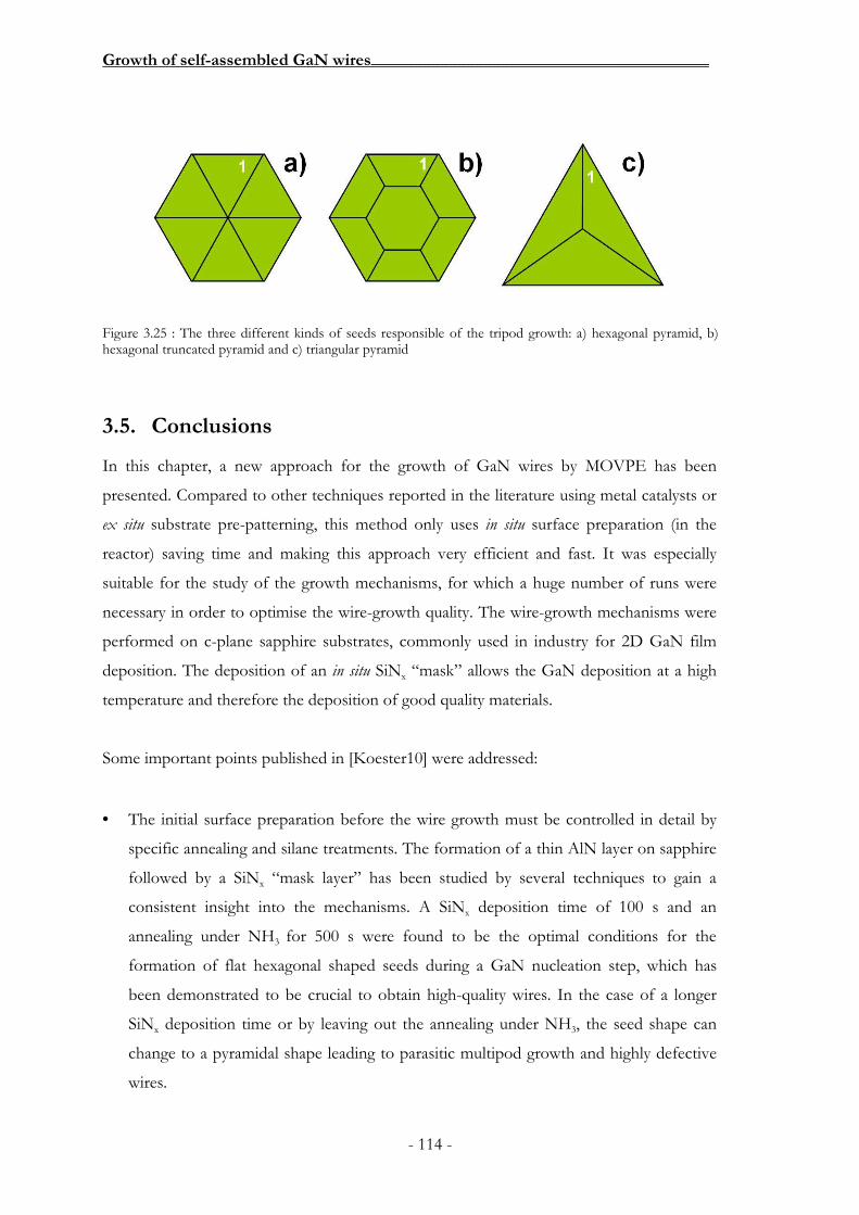
Growth of self-assembled GaN wires_______________________________________
- 114 -
3.5. Conclusions
In this chapter, a new approach for the growth of GaN wires by MOVPE has been
presented. Compared to other techniques reported in the literature using metal catalysts or
ex situ substrate pre-patterning, this method only uses in situ surface preparation (in the
reactor) saving time and making this approach very efficient and fast. It was especially
suitable for the study of the growth mechanisms, for which a huge number of runs were
necessary in order to optimise the wire-growth quality. The wire-growth mechanisms were
performed on c-plane sapphire substrates, commonly used in industry for 2D GaN film
deposition. The deposition of an in situ SiNx “mask” allows the GaN deposition at a high
temperature and therefore the deposition of good quality materials.
Some important points published in [Koester10] were addressed:
• The initial surface preparation before the wire growth must be controlled in detail by
specific annealing and silane treatments. The formation of a thin AlN layer on sapphire
followed by a SiNx “mask layer” has been studied by several techniques to gain a
consistent insight into the mechanisms. A SiNx deposition time of 100 s and an
annealing under NH3 for 500 s were found to be the optimal conditions for the
formation of flat hexagonal shaped seeds during a GaN nucleation step, which has
been demonstrated to be crucial to obtain high-quality wires. In the case of a longer
SiNx deposition time or by leaving out the annealing under NH3, the seed shape can
change to a pyramidal shape leading to parasitic multipod growth and highly defective
wires.
Figure 3.25 : The three different kinds of seeds responsible of the tripod growth: a) hexagonal pyramid, b) hexagonal truncated pyramid and c) triangular pyramid
Growth of self-assembled GaN wires_______________________________________
- 115 -
• The deposition time during the nucleation step controls the seed size. SEM and
AFM studies revealed the formation of defects by coalescence of seeds and the
lateral growth pinning on surface inhomogeneities leading to defects in the later
wire growth. For the process developed in this study, an optimal nucleation time
has been found to be close to 10 s; in that case, the seeds are small enough to
prevent coalescence.
• A low V/III ratio is essential for the wire growth. For these experiments a V/III
ratio of 16 was applied leading to optimal growth. Experiments with V/III ratios
of several hundreds gave rise to a strong lateral growth, whatever its application
from the very beginning of the growth or at a later stage. For the later device
fabrication, this behaviour could be used to coalesce the upper part of the wires
assembly.
• The wire growth itself can be carried out under the same conditions as the seed
nucleation, but with an additional injection of silane during the process. Silane is
crucial for the wire growth since it favours a longitudinal growth along the c-
direction. The optimal flow is several hundred nmol/min. The range of silane
flows (from no silane to a very large amount of silane) has been studied.
• The nucleation step and the wire growth are both carried out at 1000 °C.
Decreasing the temperature leads to a higher density of the assembly but in
parallel to a decrease in structural quality. A higher growth and nucleation
temperature leads to a strong evaporation rate of GaN making the material
deposition difficult. Within these conditions, it has been shown that the growth
rate of the wires was linear but directly influenced by the carrier gas flow rate.
The wires grown under these conditions have been studied by grazing incidence X-ray
diffraction. The experiments evidenced a growth along the c-axis and revealed the epitaxial
relationship of the wires with the surface and the typical 30 ° rotation of the GaN lattice
with respect to the sapphire with low distributions of tilt (0.61 °) and twist (0.34 °)
disorientations. STEM and CBED measurements revealed the coexistence of N- and Ga-
polar crystals inside single wires. The observed instabilities of facets for Ga-polar crystals
probably explain the top facet shape evolution of some wires and their tendency to stop
growing.

Growth of self-assembled GaN wires_______________________________________
- 116 -
SEM observations of the early stage of wire growth on non-annealed SiNx revealed
the origin of multipod formation and gave a deeper understanding of the importance of the
seed nucleation on the wire growth. The 60 ° symmetry in the multipod orientation was the
first evidence of the epitaxial relationship between the GaN growth and the sapphire
substrate finally evidenced by x-ray diffraction.

Growth of self-assembled GaN wires_______________________________________
- 117 -

Growth of self-assembled GaN wires_______________________________________
- 118 -
Chapter 4
Optical properties of GaN wires and heterostructures grown by MOVPE_________
- 119 -
4. Optical properties of GaN wires
and heterostructures grown by
MOVPE
4.1. Introduction
The use of GaN wires - and heterostructures - in optoelectronic devices like LEDs, lasers
and detectors (see chapter 1), it needs control of the optical properties of doped materials.
This chapter will be dedicated to this field which constitutes a major concern for the use of
MOCVD wires in applications.
The optical properties of “homogeneous” Si-doped wires (n-type), Si-
doped/unintentionally-doped, Si-doped/Mg-doped (p-type) and InGaN/GaN multiple
quantum well (MQW) heterostructures will be studied to demonstrate the potential use of
MOCVD wires. Single wire measurements have been chosen to analyse their intrinsic
properties. The main advantages of this approach are the removal of the parasitic signal
which may stem from the overgrowth between the wires26 and the gaining of information
concerning the location of the optical emission at different wavelengths particularly
important for heterostructures and the study of defects.
4.2. Si-doped/un-intentionally doped heterostructure growth
As already mentioned in chapter 3, the silane injection is a mandatory ingredient to fulfil
the vertical growth [Haffouz98, Frayssinet02, Koester10]. This addition leads to a strong n-
doping of the wires27. Nevertheless, it is possible to stop silane injection after the wire has
reached a certain length.
26 Due to the small density of the wires grown by the method described in chapter 3, macro-photoluminescence and cathodoluminescence measurements integrate both wire and overgrowth optical signals. 27 The n-doped feature of strongly Si-incorporated wires has been estimated by four-probe electrical measurements [Zanin09]. The very small resistivity ρ=10-3 Ω.cm-1 combined with the measured n-doped

Optical properties of GaN wires and heterostructures grown by MOVPE_________
- 120 -
Figure 4.1 shows a SEM image of such a wire growth. The initial n-doped part is
grown at 1000 °C during 1000 s with a silane molar flow corresponding to the standard
wire growth (200 nmol/min). The silane source is then switched off and the growth is
continued for 500 s by keeping the other growth parameters unchanged. A small kink is
visible in the upper part of the wire indicating the change of the growth conditions. The
wire itself keeps on growing vertically without any significant change of shape: No strong
lateral growth was observed equal to the conditions of no silane injection directly at the
beginning of the growth.
The wires were detached from the sapphire substrate by sonification in isopropanol and
then dispersed on a conducting silicon substrate. The optical properties were studied by
cathodo-luminescence (CL) measurements at Néel Institute, CNRS Grenoble28. Single
wires are excited by an electron beam with a voltage of 20 kV and a current of less then
1 nA. Figure 4.2 shows the CL spectra integrated over four zones of a 9 µm long wire with
equal areas (PO 1 to PO 4) regularly distributed along the growth axis (see inset in Figure
4.2). The PO 2 to PO 4 zones correspond to the n-doped part of the wire grown under
value of 2D layers (2-3 1019cm-3) gives a mobility value of 200 cm2 s-1 V-1 which is similar to bi-dimensional GaN (chapter 2) . 28 In collaboration with F. Donatini, J S. Hwang and D. Le Si Dang, CNRS Institut Néel Grenoble.
Figure 4.1 : Tilted (45°) SEM view of n/un-intentionally doped structures grown by stopping the silane flow after 1000 s of growth and continuing the growth for 500 s. The n-part uses the standard growth conditions given in chapter 3.

Optical properties of GaN wires and heterostructures grown by MOVPE_________
- 121 -
silane injection (about 6 µm long). The PO 1 zone corresponds to the top part of the wire
grown during 500 s (about 3 µm) without silane injection. A dominant band edge emission
(around 350 nm (3.547 eV)) can be observed all along the wire with a negligible yellow
band (YB) emission centred at 560 nm (2.217 eV). For 2D growths, the latter is commonly
assigned to gallium and oxygen complexes [Polenta07], but for the MOVPE wire growths,
a strong correlation between the observations of the band-defect emission with the
occurrence of a large amount of structural defects was generally observed. The silicon
doping coming from the silane injection produces an asymmetric band roughly centred at
350 nm (3.55 eV) nm with a broad low energy tail above the 350 nm (3.55 eV) band gap.
This effect has been demonstrated to be due to the conduction band filling effect resulting
from the heavy dopant concentration [Beaumont83, Leroux97]. Based on the optical study
of silicon doped GaN thin films [Leroux97], the FWHM of 26 nm (120 meV) of the PO2
to PO4 curves suggests a carrier concentration of above 1020/cm3 in this wire. The part of
the wire grown without silicon injection (PO 1) has an emission peak at 355 nm (3.496 eV)
and a FWHM of 14 nm (70 meV) corresponding to a carrier concentration in the 1019/cm3
range much larger than the 2D residual doping given in chapter 2 (in the 1016/cm3 range).
Therefore, it seems that silicon continues to be incorporated even after stopping the silane
flow. A possible source of this un-intentional doping may be the Si evaporation coming
from substrate overgrowth (i.e. not incorporated in silicon nitride) which can be
reincorporated mainly at the top of the wire or by Si diffusion on the wire edges or by solid
silicon diffusion.
Figure 4.2 : CL emission spectra of a single wire with n-doped and un-intentionally doped segments. The integration areas are denoted PO 1 to PO 4. The insets show a SEM viewgraph and a CL mapping measured 355 nm (3.496 eV), respectively.

Optical properties of GaN wires and heterostructures grown by MOVPE_________
- 122 -
4.3. Si/Mg-doped heterostructure growth
After the demonstration of wire growth with Si-doping variation, the Mg-doping case will
be discussed, now. Two types of growths will be discussed to study the influence of
temperature on the surface morphology and on the optical signature of the wires. Firstly,
Cp2Mg injection will be started immediately after silane injection, keeping the standard
growth temperature (1000°C). Second, the temperature will be decreased to 850 °C before
the injection of Cp2Mg.
Figure 4.3 shows tilted (45 °) SEM images of the grown structures. For the first
growth, the longitudinal wire structure was grown at 1000 °C with silane injection for the
first 1000 s, then the doping source was switched to Cp2Mg with an additional wire growth
of 500 s keeping the same temperature. The growth morphology is very similar to what has
been observed for a Si-dopant variation along the wire. For the second growth, the bottom
part of the structure was grown under silane injection at 1000 °C for 500 s. The
temperature is then decreased to 850°C with a ramp of 60 s before opening the Cp2Mg
source for 300 s. In this case, a lollypop-like morphology is observed.
Figure 4.3 : Influence of temperature on Cp2Mg–doped wire morphology. The base of the wire is grown during 1000 s (a) and 500 s (b) at 1000 °C. Then in a) Cp2Mg is injected during 500 s at the same temperature and in b) Cp2Mg is injected during 300 s after a decrease of temperature to 850 °C (a 60 s ramp is performed before opening the flow).

Optical properties of GaN wires and heterostructures grown by MOVPE_________
- 123 -
In order to study the optical properties of these two growths by CL, the wires were
detached from the sapphire substrate by sonification in an isopropanol bath and dispersed
on a conducting silicon substrate.
Figure 4.4 shows the CL spectra of a longitudinal wire taken from the first sample
shown in Figure 4.3 a). The measurements have been performed on four positions along
the wire, where PO 1 denotes the top and PO 4 the bottom region of the wire (see inset).
PO 2 to PO 4 show the characteristic n-GaN emission with a near band edge emission
centred at 350 nm (3.546 eV) and with a barley visible yellow band centred at 560 nm
(2.217 eV). The overall CL emission is strongly reduced at PO 1 and a small additional
peak can be seen centred at 375 nm (3.31 eV) next to the near band edge indicated with a
black arrow in Figure 4.4. This peak can be attributed to the donor acceptor pair (DAP)
recombination observed in p-doped GaN [Viswanath98, Reshchikov99]. The near-band
edge itself is shifted to 355 nm (3.496 eV) due to the absence of silicon doping. The inset
in Figure 4.4 shows a SEM image and its corresponding CL emission at 350 nm (3.55 eV).
The wire exhibits an overall length of 8 µm whereas the top part grown under the Cp2Mg
injection is about 2 µm long.
Figure 4.4 : CL (5 K) spectra of a longitudinal wire structure for the positions PO 1 to PO 4 indicated in the CL image (inset) measured for 350 nm emission. For comparison, the SEM image of the wire is given at the top of the inset.

Optical properties of GaN wires and heterostructures grown by MOVPE_________
- 124 -
Figure 4.5 shows the CL spectra corresponding to the second sample (see Figure 4.3 b).
The part of the wire grown under injection of silane exhibits a strong near band edge
emission (see Figure 4.5 a)) centred at 350 nm (3.546 eV) and a FWHM of 14 nm (70
meV), characteristic for heavily n-doped GaN. The yellow band is very small showing the
good optical (and structural) quality of the wire. The CL image shows that the 350 nm
emission is homogeneous over the whole wire length except at the very top region where
Cp2Mg injection occurred. Figure 4.5 b) details the emission of the top of the wire: the near
band edge emission is strongly reduced and is accompanied by an additional emission
centred at 370 nm (3.355 eV), which is about three times more intense. This region also
exhibits a very strong YB emission centred at 560 nm probably related to the low growth
temperature of 850 °C, which decreases the structural (and optical) quality of the wires.
The CL image under the spectra shows the wire emission recorded at 370 nm showing the
widened shape of the upper part of the wire. The shape of the n-doped part is also
measured due to the tail of the near band edge emission, which reaches up to 400 nm as
shown in the spectrum of Figure 4.5 a).

Optical properties of GaN wires and heterostructures grown by MOVPE_________
- 125 -
The strong peak centred at 370 nm can be attributed to the DAP recombination. The
strong increase of the signal compared to the sample displayed in Figure 4.3 a) is probably
related to the higher Mg incorporation due to the lower growth temperature. LO-phonon
replicas as reported in the literature [Viswanath98, Reshchikov99] were not observed.
These results are a first hint at successful p-doping, nevertheless further experiments (i. e.
electrical measurements and secondary ion mass spectroscopy (SIMS) on single wires) are
necessary to prove this assumption and to estimate the p-doping level. These results also
evidence the difficulty to achieve a good structural and optical quality of the Mg-doped
part. Like in 2D materials, the p-doped crystal should probably be limited to its minimal
volume in order to establish good contacts in the devices.
Figure 4.5 : a) CL (5 K) spectra of the n-doped GaN wire with a strong near band edge emission. The CL image shows the emission at 350 nm. b) CL spectra of the top of the wire grown under Cp2Mg injection at 850 °C. The spectra show an emission peak at 370 nm three times stronger than the near band edge emission and a strong yellow band centred at 560 nm. The CL image shows the emission at 370 nm.

Optical properties of GaN wires and heterostructures grown by MOVPE_________
- 126 -
4.4. InGaN/GaN multi quantum wells
InGaN/GaN MQW heterostructures constitute one of the most important building blocks
for blue and white LEDs. In this section, the growth of such InGaN/GaN
heterostructures on wire templates will be discussed in terms of morphological and optical
properties. The influence of In-concentration and quantum well thickness on the optical
properties will be studied by varying the InGaN growth temperature and time respectively.
4.4.1. InGaN/GaN MQW growth on GaN wires
The GaN wires, the growth of which was discussed in chapter 3, can be used as templates
for InGaN/GaN MQW heterostructures. The bottom of the wires is n-doped and the
structure is ended with an un-intentionally doped top part (see section 4.3). The standard
growth process for 2D InGaN/GaN MQW growth described in chapter 2 was chosen as a
first attempt to grow MQWs on the wire templates. The resulting In-incorporation,
thickness and growth morphology (radial or longitudinal heterostructures) were open
questions in this new MOVPE process.
The important features of the growth conditions can be summarised as follows: the
InGaN growth temperature is set to about 750 °C (leading to a indium incorporation of
about 18 % in 2D growth), TEG is used as a Ga precursor instead of TMG. In order to
effectuate a higher decomposition rate at a lower temperature, the reactor pressure is set to
400 mbar under N2 atmosphere instead of H2 to prevent indium etching during the growth.
For a first demonstration, the QW and QB growth times were set to 2D nominal values
corresponding to 5 nm (QW) and 10 nm (QB) thicknesses respectively.
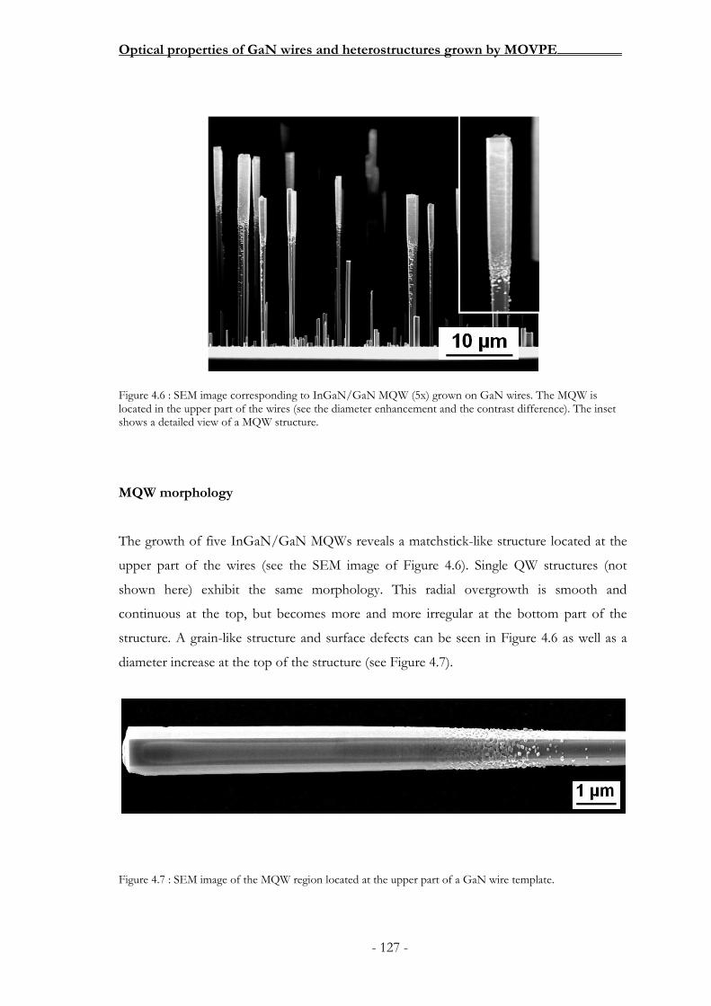
Optical properties of GaN wires and heterostructures grown by MOVPE_________
- 127 -
MQW morphology
The growth of five InGaN/GaN MQWs reveals a matchstick-like structure located at the
upper part of the wires (see the SEM image of Figure 4.6). Single QW structures (not
shown here) exhibit the same morphology. This radial overgrowth is smooth and
continuous at the top, but becomes more and more irregular at the bottom part of the
structure. A grain-like structure and surface defects can be seen in Figure 4.6 as well as a
diameter increase at the top of the structure (see Figure 4.7).
Figure 4.6 : SEM image corresponding to InGaN/GaN MQW (5x) grown on GaN wires. The MQW is located in the upper part of the wires (see the diameter enhancement and the contrast difference). The inset shows a detailed view of a MQW structure.
Figure 4.7 : SEM image of the MQW region located at the upper part of a GaN wire template.

Optical properties of GaN wires and heterostructures grown by MOVPE_________
- 128 -
Scanning transmission electron microscopy (STEM) measurements performed in the SEM
setup revealed the existence of the initial GaN wire surrounded by the InGaN/GaN
superlattice. A single wire was thinned by Focused Ion Beam (FIB) and transferred into the
SEM equipment. This surface preparation allows measurements of the wire edges but
unfortunately not the top of the wire which has been removed. Figure 4.8 shows the GaN
core of the wire and the alternating layers of InGaN and GaN on the edges. From this
STEM image, the InGaN QW (resp. GaN QB) thickness can be estimated to be about 6
nm (resp. 18 nm) showing that the lateral growth rate is not too far from the nominal 2D
values.
Figure 4.9 shows the room temperature µ-PL measurement on InGaN/GaN MQW grown
on a GaN wire (Tg = 759 °C). A strong emission peak is centred at 415 nm (2.99 eV) with a
FWHM of 26 nm (190 meV). A small emission tail reaching up to a wavelength of 500 nm
does not have a clear origin but may be attributed to the nitrogen vacancies during the
growth [Nakamura92c]. The near band edge emission located at 355 nm (3.497 eV) stems
from the un-doped GaN core. No YB emission was observed in these samples.
Figure 4.8 : STEM image of InGaN/GaN MQW grown around a GaN wire template. The enlarged picture (on the left) shows the InGaN/GaN superlattice stacking.

Optical properties of GaN wires and heterostructures grown by MOVPE_________
- 129 -
CL measurements were used to study the spatial distribution of the MQW emission. Figure
4.10 shows the CL images and spectra for heterostructures having gone through two times
spans of InGaN-QW growth 20 s and 120 s respectively with a fixed nominal QB
thickness of 10 nm (value of 2D MQW growth). As will be discussed below, it is assumed
that this change of duration will be proportional to the change of thickness. The top of the
figure shows standard SEM images taken in the CL setup illustrating the overall shape and
size of the wire. The CL graphs at the bottom of the figure show the CL spectra for seven
different positions along the MQW heterostructure. The sample holder was maintained at a
fixed position allowing a comparison of the spatial distribution at the different
wavelengths. Positions PO 1 and PO 7 are indicated by arrows in the SEM viewgraphs.
The positions PO 2 to PO 6 lie in-between these two positions.
Four main emission features can be directly identified in the CL spectra:
• 348-350 nm emission corresponding to the n-GaN NBE (a,b))
• 356-358 nm emission corresponding to the u-GaN NBE (c,d)
• a broad and intense peak around 400 nm related to the InGaN QW emission (e,f)
• a yellow band centred at 560 nm commonly attributed to defects (and generally to
the deep-level acceptors) (g,h).
Figure 4.9 : Room temperature µ-PL spectra of a 5 x InGaN/GaN MQW grown on a GaN wire template.
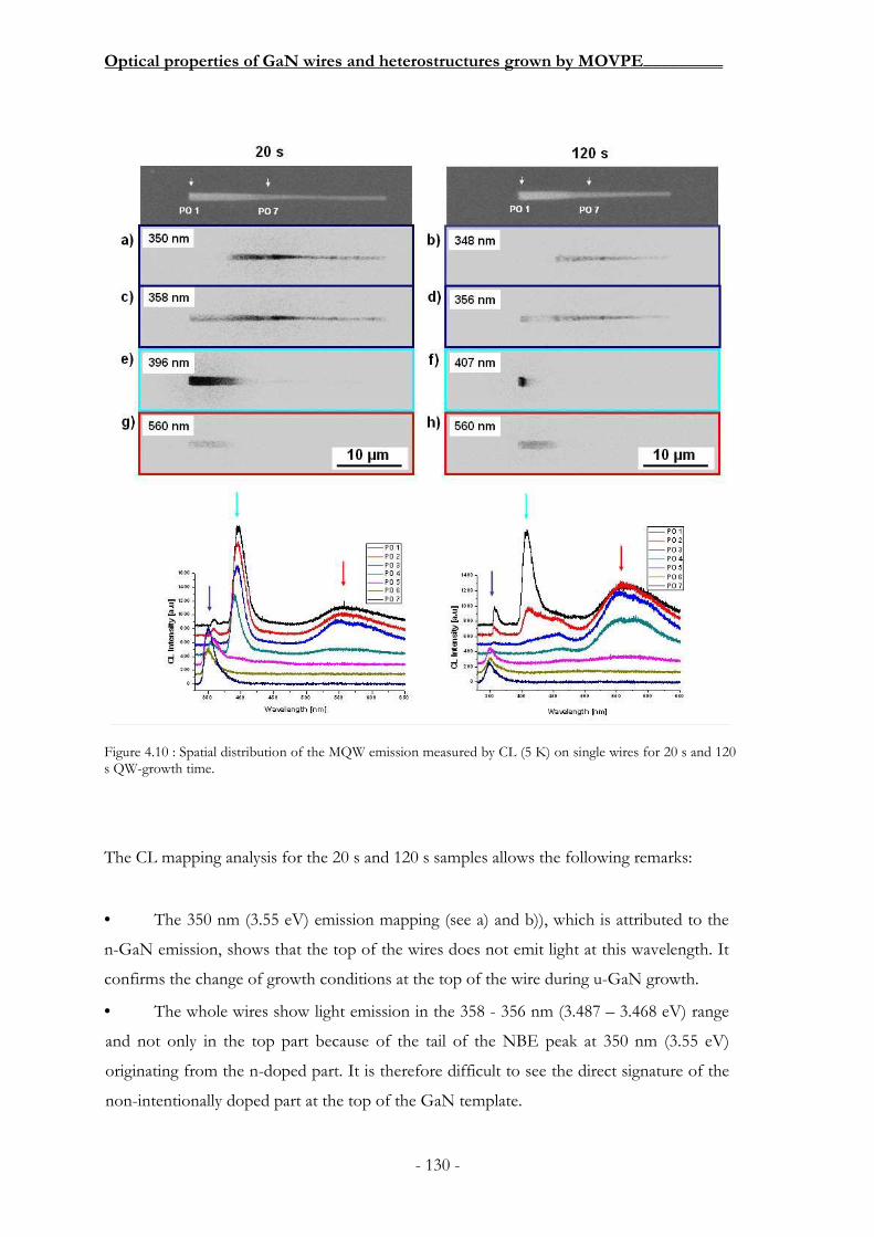
Optical properties of GaN wires and heterostructures grown by MOVPE_________
- 130 -
The CL mapping analysis for the 20 s and 120 s samples allows the following remarks:
• The 350 nm (3.55 eV) emission mapping (see a) and b)), which is attributed to the
n-GaN emission, shows that the top of the wires does not emit light at this wavelength. It
confirms the change of growth conditions at the top of the wire during u-GaN growth.
• The whole wires show light emission in the 358 - 356 nm (3.487 – 3.468 eV) range
and not only in the top part because of the tail of the NBE peak at 350 nm (3.55 eV)
originating from the n-doped part. It is therefore difficult to see the direct signature of the
non-intentionally doped part at the top of the GaN template.
Figure 4.10 : Spatial distribution of the MQW emission measured by CL (5 K) on single wires for 20 s and 120 s QW-growth time.
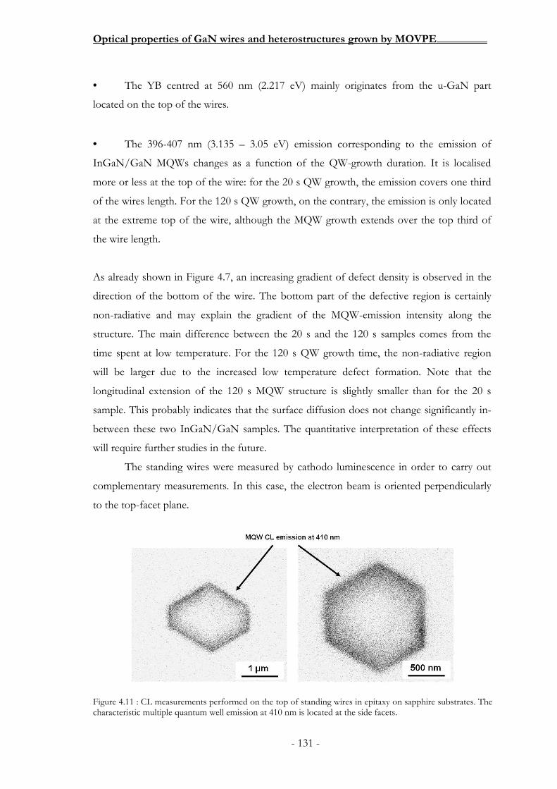
Optical properties of GaN wires and heterostructures grown by MOVPE_________
- 131 -
• The YB centred at 560 nm (2.217 eV) mainly originates from the u-GaN part
located on the top of the wires.
• The 396-407 nm (3.135 – 3.05 eV) emission corresponding to the emission of
InGaN/GaN MQWs changes as a function of the QW-growth duration. It is localised
more or less at the top of the wire: for the 20 s QW growth, the emission covers one third
of the wires length. For the 120 s QW growth, on the contrary, the emission is only located
at the extreme top of the wire, although the MQW growth extends over the top third of
the wire length.
As already shown in Figure 4.7, an increasing gradient of defect density is observed in the
direction of the bottom of the wire. The bottom part of the defective region is certainly
non-radiative and may explain the gradient of the MQW-emission intensity along the
structure. The main difference between the 20 s and the 120 s samples comes from the
time spent at low temperature. For the 120 s QW growth time, the non-radiative region
will be larger due to the increased low temperature defect formation. Note that the
longitudinal extension of the 120 s MQW structure is slightly smaller than for the 20 s
sample. This probably indicates that the surface diffusion does not change significantly in-
between these two InGaN/GaN samples. The quantitative interpretation of these effects
will require further studies in the future.
The standing wires were measured by cathodo luminescence in order to carry out
complementary measurements. In this case, the electron beam is oriented perpendicularly
to the top-facet plane.
Figure 4.11 : CL measurements performed on the top of standing wires in epitaxy on sapphire substrates. The characteristic multiple quantum well emission at 410 nm is located at the side facets.

Optical properties of GaN wires and heterostructures grown by MOVPE_________
- 132 -
Figure 4.11 shows two CL images taken at a wavelength of 410 nm corresponding to the
MQW emission of this sample. The hexagonal shape of the wires is clearly visible and the
side facets exhibit a strong emission. The top c-facet exhibits no MQW emission at this
wavelength, indicating the absence of active material on the top.
Combining this information with the CL emission mappings measured on the
dispersed wires and by SEM and STEM observations, core-shell geometry of the MQW
growth around the top part of the wire template can be concluded. A schematic of the
structure is given in Figure 4.12. The MQW superlattice is grown around the wire and an
about the superlattice thickness gradient between the top and the bottom of the active
MQW remains hitherto impossible. But it seems that the non-radiative part has a bad
structural quality, which is deteriorated into a grain-like structure at the bottom of the
MQW.
Figure 4.12 : Schematic view of an InGaN/GaN MQW grown by MOVPE around a GaN wire template. The black lines in the MQW structure represent defects. The wire n-GaN part is two times longer than the MQW region (not shown here).
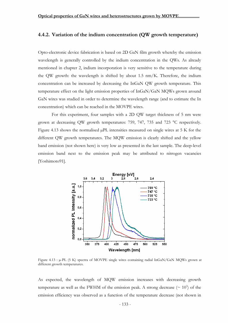
Optical properties of GaN wires and heterostructures grown by MOVPE_________
- 133 -
4.4.2. Variation of the indium concentration (QW growth temperature)
Opto-electronic device fabrication is based on 2D GaN film growth whereby the emission
wavelength is generally controlled by the indium concentration in the QWs. As already
mentioned in chapter 2, indium incorporation is very sensitive to the temperature during
the QW growth: the wavelength is shifted by about 1.5 nm/K. Therefore, the indium
concentration can be increased by decreasing the InGaN QW growth temperature. This
temperature effect on the light emission properties of InGaN/GaN MQWs grown around
GaN wires was studied in order to determine the wavelength range (and to estimate the In
concentration) which can be reached in the MOVPE wires.
For this experiment, four samples with a 2D QW target thickness of 5 nm were
grown at decreasing QW growth temperatures: 759, 747, 735 and 723 °C respectively.
Figure 4.13 shows the normalised µPL intensities measured on single wires at 5 K for the
different QW growth temperatures. The MQW emission is clearly shifted and the yellow
band emission (not shown here) is very low as presented in the last sample. The deep-level
emission band next to the emission peak may be attributed to nitrogen vacancies
[Yoshimoto91].
As expected, the wavelength of MQW emission increases with decreasing growth
temperature as well as the FWHM of the emission peak. A strong decrease (~ 103) of the
emission efficiency was observed as a function of the temperature decrease (not shown in
Figure 4.13 : µ-PL (5 K) spectra of MOVPE single wires containing radial InGaN/GaN MQWs grown at different growth temperatures.
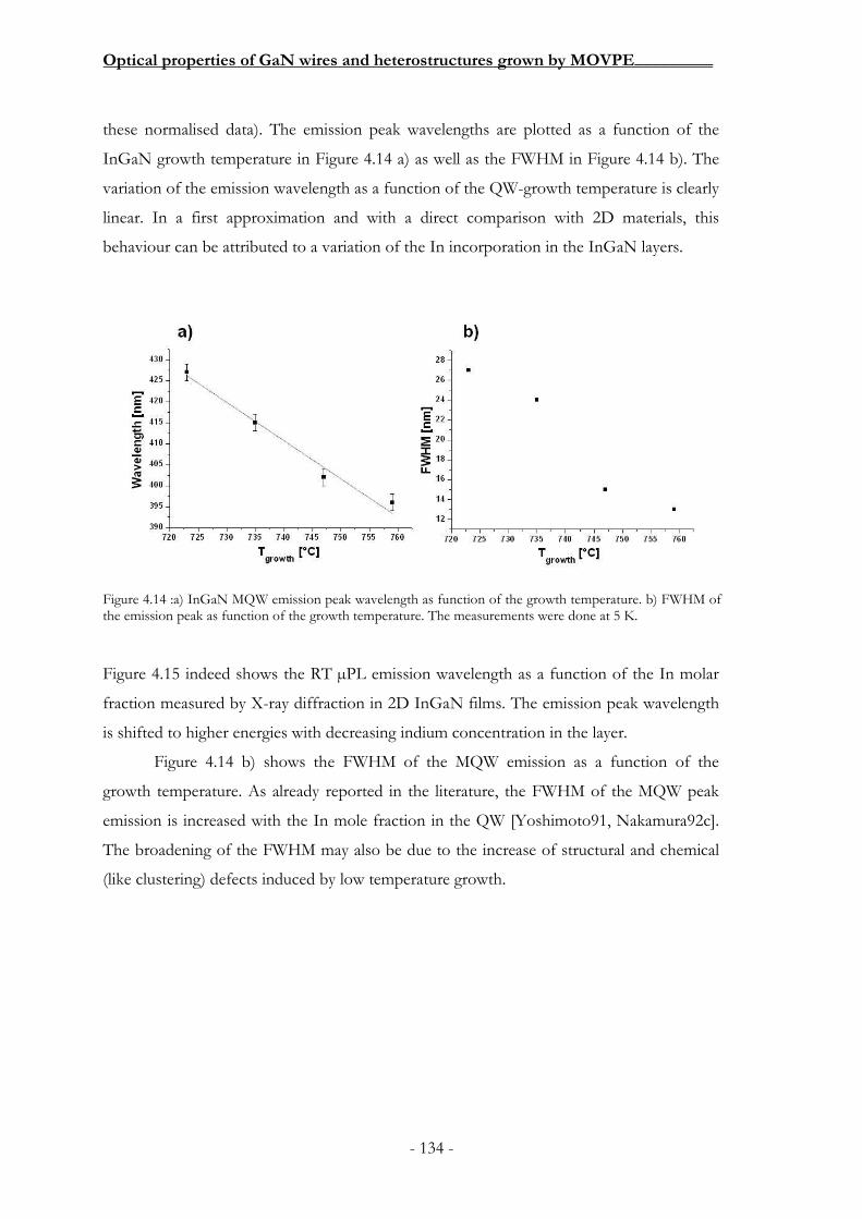
Optical properties of GaN wires and heterostructures grown by MOVPE_________
- 134 -
these normalised data). The emission peak wavelengths are plotted as a function of the
InGaN growth temperature in Figure 4.14 a) as well as the FWHM in Figure 4.14 b). The
variation of the emission wavelength as a function of the QW-growth temperature is clearly
linear. In a first approximation and with a direct comparison with 2D materials, this
behaviour can be attributed to a variation of the In incorporation in the InGaN layers.
Figure 4.15 indeed shows the RT µPL emission wavelength as a function of the In molar
fraction measured by X-ray diffraction in 2D InGaN films. The emission peak wavelength
is shifted to higher energies with decreasing indium concentration in the layer.
Figure 4.14 b) shows the FWHM of the MQW emission as a function of the
growth temperature. As already reported in the literature, the FWHM of the MQW peak
emission is increased with the In mole fraction in the QW [Yoshimoto91, Nakamura92c].
The broadening of the FWHM may also be due to the increase of structural and chemical
(like clustering) defects induced by low temperature growth.
Figure 4.14 :a) InGaN MQW emission peak wavelength as function of the growth temperature. b) FWHM of the emission peak as function of the growth temperature. The measurements were done at 5 K.

Optical properties of GaN wires and heterostructures grown by MOVPE_________
- 135 -
The In-concentration in the presented QWs can be roughly estimated from the InGaN PL
emission peak wavelength in Figure 4.15, supposing that quantum and localisation effects
do not play an important role in these samples29. The RT MQW emission reported in
Figure 4.9 is located at 415 nm (2.99 eV) which gives, in comparison with Figure 4.15, an
In concentration of 18 %. We can assume that the indium concentration in the QWs is in
the same order of magnitude as in 2D structures grown at the same temperature.
4.4.3. Variation of the QW thickness by changing the QW growth time
The CL spectra in Figure 4.10 revealed different MQW emission curves for the two
different QW growth times. For 20 s of QW growth, the maximum is close to 396 nm
(3.135 eV), whereas for 120 s of deposition, the peak is centred at 407 nm (3.05 eV). For a
deeper understanding, the MQW emission, the 80 s and 40 s intermediate values of QW
deposition times were also measured by CL. In Figure 4.16, the normalised MQW CL
spectra are plotted as a function of the wavelength. A shift to lower wavelengths is
observable with decreasing QW growth time, which becomes stronger for low QW
deposition times (40 s and 20 s). Figure 4.17 plots the position of the maximum of the
emission peak as a function of the QW growth time. For deposition times longer than 80 s,
the emission wavelength does not change significantly. For shorter growth times, a drastic
29 QW target thickness is 5 nm
Figure 4.15: RT PL emission wavelengths of InGaN 2D layers as a function of the indium mole fraction measured by X-ray diffraction [Nakamura92c].

Optical properties of GaN wires and heterostructures grown by MOVPE_________
- 136 -
drop of the emission wavelength can be seen. The FWHM of the CL emission is about 20
nm (see Table 4.1) and does not vary with the growth time, contrary to the dependency on
the indium concentration at a given thickness (see section 4.4.2).
This observation tends to indicate that the In-concentration in the QW is roughly constant
in all the samples and that the shift of the emission peak should not be attributed to a
change of the InGaN alloy composition. It can be most probably attributed to a decrease
of the QW thickness with decreasing growth time30, which leads to a quantum confinement
[Takeuchi97, Chichibu99]. Table 4.1 gives the nominal QW thickness corresponding to
2D growth on the c-plane surface for the different growth times, the measured emission
wavelength and the corresponding FWHM.
30 The precise measurements of the core/shell superlattice thicknesses are under way. MOVPE grown samples are too thick to be directly measured by TEM without any thinning. Focused Ion Beam (FIB) preparations will be performed to obtain longitudinal slices of the wires. They will allow the comparison of the real thickness values with the nominal ones and the verification of the proportionality of growth time and thickness on the m-plane edges of the wires. SIMS profiling is also under way with 2D references to obtain these values.
Figure 4.16 : MQW (x 5) CL (5 K) spectra for several QW growth times (20 to 120 s). The QW target thickness is 5 nm.

Optical properties of GaN wires and heterostructures grown by MOVPE_________
- 137 -
QW growth
time (s)
Nominal QW thickness (nm)
target value for 2D (0001) growth
Emission wavelength (nm) FWHM
(nm)
120 7.5 408.3 20
80 5 407.3 19
40 2.5 404.7 20
20 1.25 396.5 19
Table 4.1 : QW growth time, nominal QW thickness from 2D growth in [0001] direction, CL (5 K) MQW emission wavelength and corresponding FWHM.
Figure 4.17 a) and b) respectively show the MQW emission wavelength and energy as a
function of the QW growth time. For longer QW growth times, the emission peak position
has an asymptotic behaviour to reach a value of about 408 nm (3.04 eV).
Figure 4.18 shows the calculated QW emission energy and the PL measurements for an
In0.13Ga0.87N/Ga0.97In0.03N MQW grown in c-plane direction as a function of the QW
thickness [Takeuchi97]. The solid curve represents the peak evolution under the presence
of a piezoelectric field of 1.08 MV/cm. The transition energy without any electric field is
shown by the dashed line. The white and black squares represent PL measurements with
low (2 W/cm2) and high (200 kW/cm2) excitation power for different QW thicknesses.
Figure 4.17 : a) Wavelength and b) energy evolution of InGaN QW transition as a function of growth time. These CL measurements have been obtained at 5K.
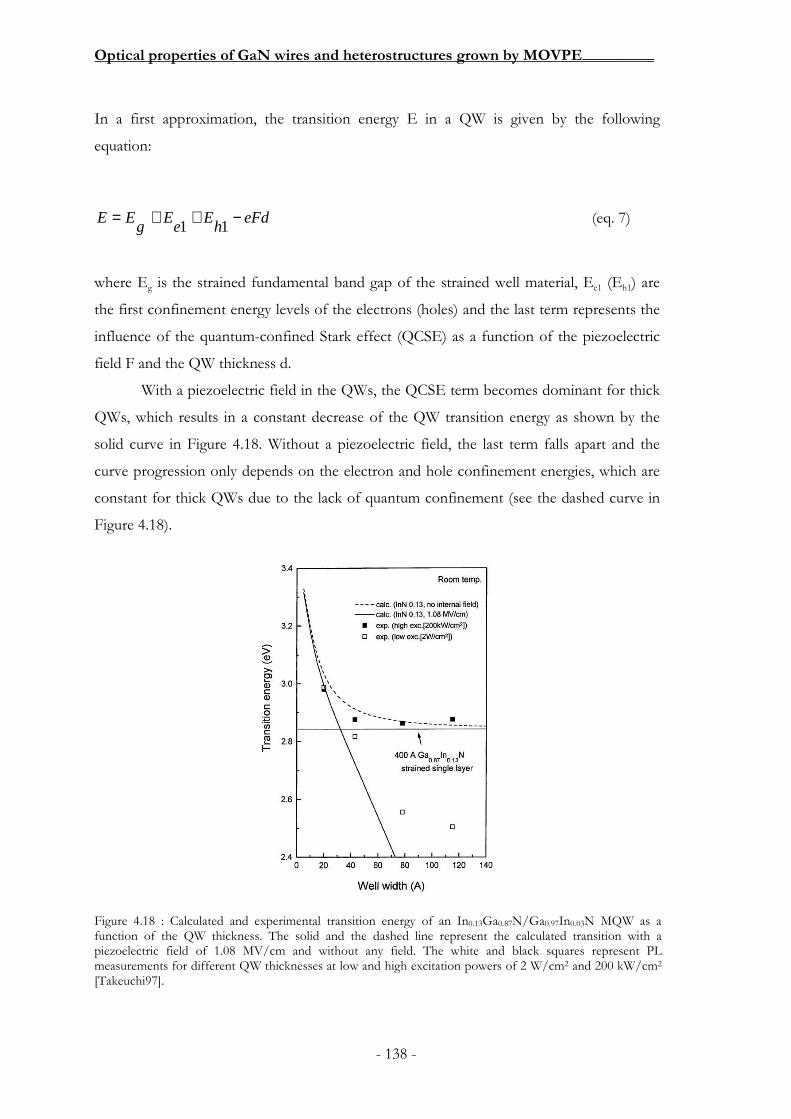
Optical properties of GaN wires and heterostructures grown by MOVPE_________
- 138 -
In a first approximation, the transition energy E in a QW is given by the following
equation:
eFdh
Ee
Eg
EE −++=11
(eq. 7)
where Eg is the strained fundamental band gap of the strained well material, Ee1 (Eh1) are
the first confinement energy levels of the electrons (holes) and the last term represents the
influence of the quantum-confined Stark effect (QCSE) as a function of the piezoelectric
field F and the QW thickness d.
With a piezoelectric field in the QWs, the QCSE term becomes dominant for thick
QWs, which results in a constant decrease of the QW transition energy as shown by the
solid curve in Figure 4.18. Without a piezoelectric field, the last term falls apart and the
curve progression only depends on the electron and hole confinement energies, which are
constant for thick QWs due to the lack of quantum confinement (see the dashed curve in
Figure 4.18).
Figure 4.18 : Calculated and experimental transition energy of an In0.13Ga0.87N/Ga0.97In0.03N MQW as a function of the QW thickness. The solid and the dashed line represent the calculated transition with a piezoelectric field of 1.08 MV/cm and without any field. The white and black squares represent PL measurements for different QW thicknesses at low and high excitation powers of 2 W/cm2 and 200 kW/cm2 [Takeuchi97].
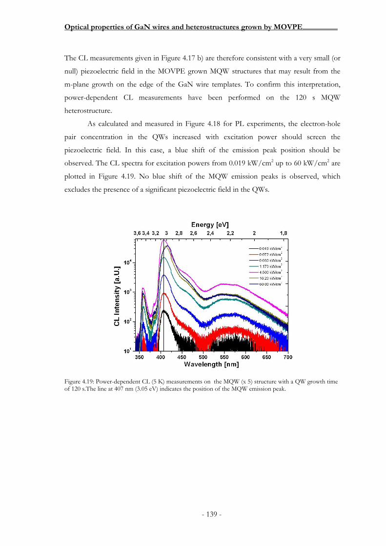
Optical properties of GaN wires and heterostructures grown by MOVPE_________
- 139 -
The CL measurements given in Figure 4.17 b) are therefore consistent with a very small (or
null) piezoelectric field in the MOVPE grown MQW structures that may result from the
m-plane growth on the edge of the GaN wire templates. To confirm this interpretation,
power-dependent CL measurements have been performed on the 120 s MQW
heterostructure.
As calculated and measured in Figure 4.18 for PL experiments, the electron-hole
pair concentration in the QWs increased with excitation power should screen the
piezoelectric field. In this case, a blue shift of the emission peak position should be
observed. The CL spectra for excitation powers from 0.019 kW/cm2 up to 60 kW/cm2 are
plotted in Figure 4.19. No blue shift of the MQW emission peaks is observed, which
excludes the presence of a significant piezoelectric field in the QWs.
Figure 4.19: Power-dependent CL (5 K) measurements on the MQW (x 5) structure with a QW growth time of 120 s.The line at 407 nm (3.05 eV) indicates the position of the MQW emission peak.

Optical properties of GaN wires and heterostructures grown by MOVPE_________
- 140 -
4.5. Conclusions
The optical properties of several wire-based heterostructures were studied in this chapter.
n/un-intentionally doped axial heterostructures were produced by stopping the
silane flow after the first part of the wire had been grown under silane injection. To
maintain the wire geometry, this stop of silane injection can only be performed after the n-
doped part has reached a length of at least 5 µm. Stopping the silane flow at an earlier stage
of the growth leads to the formation of GaN island with a strong lateral growth.
CL measurements (5 K) revealed a characteristic n-GaN emission over the bottom
part of the wire grown under silane injection: the near band edge emission is located at 350
nm (3.55 eV) with a FWHM of 16 nm (120 meV) indicating a doping level of about
1020/cm3. A continuation of the growth without silane injection (maintaining the growth
temperature of 1000 °C) does not lead to a significant change of the wire shape. The NBE
emission is more intense and shifted to 355 nm (3.496 eV) with a FWHM of about 7 nm
(70 meV). A carrier concentration in the 1019/cm3 range can be estimated and it can be
concluded that this part is un-intentionally n-doped in practice.
n-doped/Mg-doped heterostructures were realised by Cp2Mg injection at the n-
doped top part of the wire. The growth temperature of the Mg-doped part was shown to
be very important for both structural and optical properties (growth temperatures of 1000
°C and 850 °C were tested).
CL measurements reveal a very weak emission at the Mg-doped top part of the
wires: an emission peak at 375 nm (3.31 eV) can be observed close to the near band edge
emission at 355 nm (3.497 eV). At high temperature growth (1000 °C), the wire geometry is
preserved (like the n/un-intentionally doped heterostructure) whereas the growth at lower
temperature (850 °C) leads to the formation of a lollypop-like morphology on top of the
wire (with enhanced lateral growth). CL measurements on top of a wire grown at 850 °C
show a 370 nm (3.36 eV) emission peak similar to the peak observed for the growth at
1000 °C but with a much stronger intensity. These emission peaks can be attributed to the
DAP transition and can be taken as a first hint of successful p-doping of the material. The
increase of the DAP emission with decreasing growth temperature leads to the conclusion
of the decrease of Mg incorporation with increasing growth temperature.
Complementary experiments in terms of secondary ion mass spectroscopy (SIMS)
on single wires and electrical measurements to estimate the dopant concentrations and

Optical properties of GaN wires and heterostructures grown by MOVPE_________
- 141 -
activities are presently under way. The properties of p – u – n photodetector devices are
also presently studied in a project of the French Research Agency (ANR).
InGaN/GaN MQW heterostructures were deposited on wire templates by applying
the 2D MQW growth technique described in chapter 2. The spatial distribution of the
emission was studied by CL on single wires; the growth temperature was changed to vary
the indium concentration and growth time to change the QW thickness.
The MQW lateral overgrowth at the top of the wire in the core/shell geometry was
evidenced by CL and SEM observations: characteristic MQW emission is located on the
side facets and not on the wires tops. The MQW structure grows on the m-plane facets of
the wires, not along the c-direction and therefore significantly different piezo-electric
contributions influence the optical emission.
µ-PL measurements on single MQW structures with different QW growth
temperatures revealed a shift of the MQW emission peak to higher energies with increasing
growth temperature, which was attributed to a change of the In concentration.
The decrease of the QW growth time led to the blue shift of the QW transition energy
attributed to quantum confinement in the wells. The asymptotic behaviour at larger
thickness of this QW transition energy and the absence of a blue shift at a high CL
excitation power excluded the presence of a significant piezoelectric field in the QWs, in
agreement with the radial growth of InGaN/GaN MQWs on the m-plane side facets of the
GaN wires.

Optical properties of GaN wires and heterostructures grown by MOVPE_________
- 142 -
Chapter 5

Optical properties of GaN wires and heterostructures grown by MOVPE_________
- 143 -
5. Conclusions and perspectives
This work demonstrated the MOVPE catalyst-free self-assembled growth of GaN
wires.
The GaN wire growth was achieved in a new Thomas Swan (Aixtron) 3x2” CCS
MOCVD reactor. This reactor was the first one of this type in the laboratory and was
installed in 2007. The system is originally designed for bi-dimensional growth of GaN,
AlN, InN and their alloys. During the validation process of the MOCVD system, the
growth of the building blocks of blue LEDs was achieved.
• Reproducibility of the GaN layers in terms of material composition,
thickness, structural quality and homogeneity over a whole 2” sapphire
wafer was fulfilled using a low temperature GaN nucleation layer, the
standard growth method in the literature. SEM and AFM measurements
quantified the layer morphology in terms of homogeneity and roughness.
The layers are flat with a RMS of 0.42 nm over 64 µm2 and exhibit a
standard dislocation density of 2 x 108 cm-2.
• The control of n- and p-doping in GaN was achieved by convenient
concentrations for device applications. The residual n-doping of un-
intentionally doped GaN as well as related carrier mobilities were
quantified.
• InGaN/GaN MQWs grown with the MOCVD system exhibit RT PL
emission wavelengths between 442 nm and 447 nm (2.81 eV - 2.78 eV)
depending on the position on the 2” sapphire substrate. The FWHM is
about 35 nm (20 meV) and independent from the measured position. These
results confirm the homogeneity of the MQW layers in terms of
composition and quality over the whole wafer.

Conclusions and perspectives_____________________________________________
- 144 -
• After having checked that the MOCVD system fulfils the desired
specifications for GaN and InGaN growth with respect to crystal quality,
doping level and In-concentration control, these building blocks were
combined to realise a blue LED, showing a strong blue electro-
luminescence31.
The catalyst-free self-assembled approach to grow GaN wires by MOVPE, developed
during this thesis, was not reported in the literature. A systematic study was performed to
understand the key parameters controlling the growth of these one-dimensional structures.
Schematically, the developed approach can be divided into three main steps:
• (I) Surface preparation: bake, annealing under NH3 and the deposition of a thin
dielectric SiNx layer followed by an annealing under NH3
• (II) Nucleation of GaN islands
• (III) GaN wire growth.
(I) The thin dielectric SiNx layer, deposited during the surface preparation step,
behaves like a (selective) mask for the later GaN deposition. The SiNx
deposition time (100 sec where found to be close to the optimum) and the
annealing of the resulting layer under NH3 are both crucial parameters for the
wire growth.
(II) During the nucleation step, a deposition time between 10 s and 100 s was
found to be the optimum for the formation of hexagonal shaped GaN seeds,
which determine the later GaN wires’ shape and diameter.
(III) Several growth parameters were identified to be crucial for the GaN wire
growth:
• A V/III ratio lower than a few tens is essential for the wire growth: a too high
value (several hundreds) leads to lateral growth, whereas values below ten lead to
the formation of laterally growing islands.
31 Lithography and electrical contacting was performed by CEA/DOPT.

Conclusions and perspectives_____________________________________________
- 145 -
• Within the mentioned experimental conditions (in particular: a low hydrogen
content in the carrier gas, and no patterned surface for selective area growth), the
wire growth is only observed under injection of silane. The optimal silane flow was
found to be several hundreds of nmol/min. A too low silane flow leads to strong
lateral growth and for flows of several thousands of nmol/min, the structural
quality (and morphology) of the wires is strongly degraded.
• The growth temperature affects the structural quality of the wires. The wires’
structural quality is good at a high temperature (1000 °C) growth, but a decrease of
only some tens of degrees leads to an increase of structural defects (kinks along the
wires, irregular shapes…) accompanied by an increase of the wire density. A higher
temperature leads to material evaporation without the formation of wires.
• Within these optimised growth conditions, the growth rate is constant but strongly
dependent on the carrier-gas flow: a decrease of the carrier-gas flow increases the
dwell time of the materials in the reactor and leads to a large increase of the wire-
growth rate.
From the structural point of view, the as-grown wires have been studied by grazing
incident x-ray diffraction. The experiments evidenced the wires’ growth direction along the
c-axis and revealed the epitaxial relationships of the wires with the substrate. The wires
show the typical 30 ° rotation of the GaN lattice with respect to the sapphire, and the
assembly has a low distribution of tilt- and twist-disorientations corresponding to about
0.61 and 0.34 ° FWHM respectively. STEM and CBED measurements revealed the
coexistence of N- and Ga-polar crystalline c-orientations in the wires. It is proposed that
the instabilities of the Ga-polar facets may explain the evolution of the top wire facets and
their tendency to stop growing.
To conclude, the developed approach may be viewed as a fast and reproducible
technique to grow GaN wires by MOVPE. Compared to other techniques, it allows the
systematic study of the growth parameters’ influence without being dependent on time
consuming ex situ surface preparations like surface patterning used in SAG. Nevertheless,
the controls of density and the diameter distribution as well as the reduction of the
overgrowth in-between the wires have not been completely solved.

Conclusions and perspectives_____________________________________________
- 146 -
The growth of heterostructures as longitudinal n-u and “n-p” wires as well as a
core-shell InGaN/GaN MQW using the wires as templates was demonstrated.
The longitudinal n/un-intentionally doped heterostructures were grown by
stopping the silane flow after the wires had reached a length of about 5 µm. At this stage of
the growth, the absence of silane does not lead to lateral growth which would occur
without silane injection directly at the beginning of the growth. The doping variation in the
longitudinal structure was evidenced by cathodo luminescence measurements on single
wires at 5 K. The bottom part of the wire, grown under silane injection, shows a near band
edge emission located at 350 nm (3.55 eV) with a FWHM of 16 nm (120 meV) consistent
with a doping level of about 1020 cm-3. This value has been confirmed by electrical
transport measurements on single wires at the Néel Institute, CNRS Grenoble. A
continuation of the growth without silane injection (maintaining the growth temperature at
1000 °C) does not result in a significant change of the wire shape. The NBE emission is
shifted to 355 nm (3.496 eV) with a FWHM of about 7 nm (70 meV) indicating a carrier
concentration of about 1019 cm-3. It can be concluded that this part is un-intentionally
n-doped at a much higher level than the conventional un-doped layers (around 1016 cm-3).
In parallel, an attempt was taken to develop n-p heterostructures by switching from
silane to Cp2Mg and keeping the other growth conditions fixed. At a growth temperature
of 1000 °C, the wires’ geometry is preserved (like for the n/un-intentionally doped
heterostructure) whereas the growth at a lower temperature (850 °C) leads to a lollypop-like
morphology on top of the wire. CL measurements revealed a small emission peak centred
at 375 nm (3.31 eV) next to the NBE emission centred at 355 (3.496 eV) for the structure
grown at 1000 °C and a peak with a larger intensity at 370 nm (3.36 eV) for the structure
grown at 850 °C. These emission peaks can be attributed to the DAP transition and can be
taken as a first hint for successful p-doping of the material. Electrical measurements now
have to be performed to confirm these preliminary experiments.
InGaN/GaN MQW heterostructures were grown on wire templates by applying
the 2D MQW growth parameters. The spatial distribution of the QW emission was studied
on single wires by µPL and CL. The In-concentration in the QWs and their thickness was
controlled by changing the QW growth temperature and growth time respectively. The
lateral core/shell overgrowth on top of the wires has been evidenced by SEM and CL
measurements.

Conclusions and perspectives_____________________________________________
- 147 -
The characteristic MQW emission is located at the side facets of the structure but
not on the top facet. The core/shell structure is grown on the m-plane facets of the wire
and not on the c-plane as is the case for 2D materials with the same sapphire substrate.
Consequently, different piezoelectric contributions influence the wires’ emission properties.
• µPL measurements on single MQW structures grown with different QW growth
temperatures revealed a shift of the MQW emission to higher energies with
increasing growth temperature. This shift can be attributed to a change of the
indium concentration in the QWs.
• A decrease of the QW growth time led to a blue shift of the emission attributed to
quantum confinement in the wells. The asymptotic behaviour for larger QW
thicknesses and the absence of a blue shift for higher excitation powers in that
region excludes the presence of a significant piezoelectric field in the QWs, in
agreement with the m-plane growth direction.
The growth of the fundamental building blocks of a wire-based blue LED was
demonstrated during this thesis. The realisation of an efficient device still requires
a deeper understanding and optimisation of the parameters controlling the material
growth and an optimisation of the electrical contacts, difficult to achieve directly on
sapphire substrates.
This work opens new opportunities for nitride nanowires grown by MOCVD. The control
of the diameter, position and assembly density is strongly limited by the self-assembled
approach described in this thesis. A possibility to overcome these limits is the use of
SAG32. The position and diameter of the wires are defined by a pre-patterned mask
generated ex situ by lithographic techniques allowing a deeper study of the nucleation and
its influence on wire growth. Experiments with different assembly densities could clarify
how the material is incorporated at the top of the wire structure and what the role of
surface diffusion is [Borgström07]. A higher density of the assembly could also allow the
coalescence of the top of the wires to obtain a bi-dimensional layer, much more convenient
for later electrical contacting of the devices. 32 This SAG approach, using nano-imprint for substrate patterning is presently under development by
Xiaojun Chen (PhD student, CEA Grenoble INAC/SP2M/NPSC).

Conclusions and perspectives_____________________________________________
- 148 -
Doping control, especially the growth of intrinsic materials and p-doping, still has to be
optimised. In the case of p-doping, the incorporation of Mg and its activation after
annealing has to be confirmed electrically. These results should be compared with
advanced characterisation techniques such as secondary ion mass spectrometry (SIMS), x-
ray fluorescence and electron microscopy holography performed on single wires.
Concerning the InGaN/GaN MQW growth, a few questions remain open: Why do the
materials grow in core/shell geometry and not longitudinally as is the case for MBE and
why is the core/shell structure only located in the upper third of the wire and what is the
influence of the growth parameters on this effect? To answer these questions, the influence
of the growth parameters such as temperature, pressure and carrier-gas flow should be
studied in more detail.
Finally, the growth of an AlGaN-based wire heterostructure seems to be interesting for
future explorations because of the smaller difference in growth temperature between
AlGaN and GaN compared to the InGaN/GaN system.

Optical properties of GaN wires and heterostructures grown by MOVPE_________
- 149 -
Glossary
AFM – atomic force microscopy
AM – air mass
CBED – convergent beam electron diffraction
CCS – close coupled showerhead
CL – catodoluminescence
CTR – crystal truncation rod
CVD – chemical vapour deposition
DAP – donor acceptor pair
DBR – distributed bragg reflector
EL – electroluminescence
FET – field effect transistor
FIB – focused ion beam
FWHM – full width at half maximum
HCP – hexagonal closed packed
HEMT – high electron mobility transistor
HT – high temperature
HVPE – hydrate vapour phase epitaxy
LED – light emitting diode
LEEBI – low energy electron beam irritation
LPCVD – low pressure chemical vapour deposition
LT – low temperature
MBE – molecular beam epitaxy
MO – metal organics
MOCVD – metal organic chemical vapour deposition
MO-HVPE – metal organic hydride vapour phase epitaxy
MOVPE – metal organic vapour phase epitaxy
MQW – multi quantum well
NBE – near band edge
PAA – porous anodic alumina
PL – photoluminescence

- 150 -
µPL – micro photoluminescence
QB – quantum barrier
QCSE – quantum confined stark effect
QW – quantum well
RHEED – reflection high energy electron diffraction
RMS – root mean square
RT – room temperature
SAG – selective area growth
SEM – scanning electron microscope
SIMS – secondary ion mass spectroscopy
SOG – spin-on glass
STEM – scanning transmission electron microscopy
TD – threading dislocation
TEM – transmission electron microscope
VLS – vapour liquid solid
VS – vapour solid
VSS – vapour solid solid
XPS – X-ray photoelectron spectroscopy
XRR – X-ray reflectivity
YB – yellow band
- 151 -
References
[Allwood05] D. A. Allwood, G. Xiong, C. C. Faulkner, D. Atkinson, D. Petit and R. P.
Cowburn, Magnetic Domain-Wall Logic, Science 309 1688 (2005)
[Amano89] H. Amano, M. Kito, K. Hiramatsu, P-Type Conduction in Mg-Doped GaN Treated
with Low-Energy Electron Beam Irradiation (LEEBI), Japanese Journal of Applied Physics 28
2112 (1989)
[Amano98] H. Amano, M. Iwaya, T. Kashima, M. Katsuragawa, I. Akasaki, J. Han, S.
Hearne, J. A. Floro, E. Chason and J. Figiel, Stress and Defect Control in GaN Using Low
Temperature Interlayers, Japanese Journal of Applied Physics 37 1540 (1998)
[Ambacher98] O. Ambacher, Growth and applications of Group III nitrides, Journal of
Physics D 31 2653 (1998)
[Ambacher00] O. Ambacher, B. Foutz, J. Smart, J. R. Shealy, N. G. Weimann, K. Chu, M.
Murphy, A. J. Sierakowski, W. J. Schaff, L. F. Eastman, R. Dimitrov, A. Mitchell and M.
Stutzmann, Two dimensional electron gases induced by spontaneous and piezoelectric polarization in
undoped and doped Al-GaN/GaN heterostructures, Journal of Applied Physics 87 334 (2000)
[Ambacher02] O. Ambacher, J. Majewski, C. Miskys, A. Link, M. Hermann, M. Eickhoff,
M. Stutzmann, F. Berardini, V. Fiorentini, V. Tilak, B. Schaff and L. F. Eastman, Pyroelectric
properties of Al(In)GaN/GaN hetero- and quantum well structures, Journal of Physics: Condensed
Matter 14 3399 (2002)
[Aschenbrenner09] T. Aschenbrenner, C. Kruse, G. Kunert, S. Figge, K. Sebald, J. Kalden,
T. Voss, J. Gutowski and D. Hommel, Highly ordered catalyst-free and mask-free GaN nanorods on
r-plane sapphire, Nanotechnology 20 075604 (2009)
- 152 -
[Avramescu09] A. Avramescu, T. Lermer, J. Müller, S. Tautz, D. Queren, S. Lutgen and U.
Strauß, InGaN laser diodes with 50 mW output power emitting at 515 nm, Applied Physics Letters
95 071103 (2009)
[Barrelet04] C. J. Barrelet, A. B. Greytak and C. M. Lieber, Nanowire Photonic Circuit Elements,
Nano Letters 4 1981 (2004)
[Beaumont83] B. Beaumont, G. Nataf, J. C. Guillaume and C. Verie, Low temperature
photoluminescence of n-type GaInAsP layers grown on InP by liquid phase epitaxy, Journal of Applied
Physics, 54 5363 (1983)
[Beaumont98] B. Beaumont, M. Vaille, G. Nataf, A. Bouillé, J.-C. Guillaume, P.
Vénnègues, S. Haffouz and P. Gibart, Mg-enhanced lateral overgrowth of GaN on patterned
GaN/sapphire substrate by selective Metal Organic Vapor Phase Epitaxy, MRS Internet Journal
Nitride Semiconductor Research 3 20 (1998)
[Berkowicz00] E. Berkowicz, D. Geshoni, G. Bahir, E. Lakin, D. Shilo, E. Zolotoyabko, A.
Abare, S. DenBaars, L. Coldren, Measured and calculated radiative lifetime and optical absorption of
InxGa1-xN/GaN quantum structures, Physical Review B 61 10994 (2000)
[Bernardini97] F. Bernardini, V. Fiorentin and D. Vanderbilt, Spontaneous polarization and
piezoelectric constants of III-V nitrides, Physical Review B 56 10024 (1997)
[Bertness06] K. A. Bertness, A. Roshko, N. A. Sanford, J. M. Barker and A. V. Davydov,
Spontaneously grown GaN and AlGaN nanowires, Journal of Crystal Growth 287 522 (2006)
[Bloom74] S. Bloom, G. Harbeke, E. Meier and I. Ortenbur, Band-structure and reflectivity of
GaN, Physica Status Solidi B-Basic Research 66 161 (1974)
[Borgström07] M. T. Borgström, G. Immink, B. Ketelaars, R. Algra and E. P. A. M.
Bakkers, Synergetic nanowire growth, Nature Nanotechnology 2 541 (2007)
- 153 -
[Bougrioua07] Z. Bougrioua, P. Gibart, E. Calleja, A. Trampert, J. Ristic, M. Utrera and G.
Nataf, Growth of freestanding GaN using pillar-epitaxial lateral overgrowth from GaN nanocolumns,
Journal of Crystal Growth 309 113 (2007)
[Caetano07] C. Caetano, L. K. Teles, M. Marques, A. D. Pino and L. G. Ferreira, Theoretical
support for the smaller band gap bowing in wurtzite InGaN alloys, AIP Conference Proceeding 893
257 (2007)
[Calleja00] E. Calleja, M. A. Sanchez-Garcia, F. J. Sanchez, F. Calle, F. B. Naranjo and E.
Munoz, Luminescence properties and defects in GaN nanocolumns grown by molecular beam epitaxy,
Physical Review B 62(24) (2000)
[Chemla83] D. S. Chemla, T. C. Damen, D. A. B. Miller, A. C. Gossard and W. Wiegmann,
Electroabsorption by Stark effect on room-temperature excitons in GaAs/GaAlAs multiple quantum well
structures, Applied Physics Letters 42 864 (1983)
[Chen04] Z. Chen, Z. Shan, M. S. Cao, L. Lu and S. X. Mao, Zinc oxide nanotetrapods,
Nanotechnology 15 365 (2004)
[Cheng07] A. T. Cheng, Y. K. Su and W. C. Lai, MOVPE growth of InGaN/GaN multiple
quantum wells for the blue laser diode applications, Journal of Crystal Growth 298 508 (2007)
[Chichibu99] S. F. Chichibu, A. C. Abare, M. P. Mack, M. S. Minsky, T. Deguchi, D.
Cohen, P. Kozodoy, S. B. Fleischer, S. Keller, J. S. Speck, J. E. Bowers, E. Hu, U. K.
Mishra, L. A. Coldren, S. P. DenBaars, K. Wada, T. Sota and S. Nakamura, Optical properties
of InGaN quantum wells, Material Science and Engineering B 59 298 (1999)
[Chichibu00] S. Chichibu, A. Shikanai, T. Deguchi, A. Setoguchi, R. Nakai, H. Nakanishi,
K. Wada, S. DenBaars, T. Sota and S. Nakamura, Comparison of Optical Properties of
GaN/AlGaN and InGaN/AlGaN Single Quantum Wells, Japanese Journal of Applied Physics
39 2417 (2000)
[Chien96] F. R. Chien, X. J. Ning, S. Stemmer, P. Pirouz, M. D. Bremser and R. F. Davis,
Growth defects in GaN films on 6H–SiC substrates, Applied Physics Letters 68 2678 (1996)

- 154 -
[Cierchia03] R. Chierchia, T. Böttcher, H. Heinke, S. Einfeldt, S. Figge and D. Hommel,
Microstructure of heteroepitaxial GaN revealed by x-ray diffraction, Journal Applied Physics 93 8918
(2003)
[Cordier09] Y. Cordier, F. Semond, J. - C. Moreno, E. Frayssinet, B. Benbakhti, Z. Cao, S.
Chenot, L. Nguyen, O. Tottereau, A. Soltani, K. Blary, Selective area growth of GaN-based
structures by molecular beam epitaxy on micrometer and nanometer size patterns, Materials Science in
Semiconductor Processing 12 16 (2009)
[Daulesberg08] M. Dauelsberg, C. Martin, H. Protzmann, A. R. Boyd, E. J. Thrush, J.
Kaeppeler, M. Heuken, R. A. Talalaev, E. V. Yakovlev and A. V. Kondratyev, Modeling and
process design of III-Nitride MOVPE at near-atmospheric pressure in Close Coupled Showerhead and
Planetary Reactors, ICMOVPE 13 poster (2008)
(http://aixtron.com/fileadmin/user_upload/pdf/Publications/ICMOVPE_13__Poster__
Modeling_GaN_High_Pressure_MOVPE.pdf)
[Deb05] P. Deb, H. Kim, V. Rawat, M. Oliver, S. Kim, M. Marshall, E. Stach and T. Sands,
Faceted and Vertically Aligned GaN Nanorod Arrays Fabricated without Catalysts or Lithography,
Nano Letter 5(9) 1847 (2005)
[Dobrokhotov06] V. Dobrokhotov D. N. McIlroy, M. G. Norton, A. Abuzir, W. J. Yeh, I.
Stevenson, R. Pouy, J. Bochenek, M. Cartwright, L. Wang,J. Dawson, M. Beaux and C.
Berven, Principles and mechanisms of gas sensing by GaN nanowires functionalized with gold
nanoparticles, Journal of Applied Physics 99 104302 (2006)
[Domracheva08] Y. V. Domracheva, V. N. Jmerik, T. B. Popova and
M. V. Zamoryanskaya, Cathodoluminescent investigations of InxGa1-xN layers, Journal of Materials
Science: Materials in Electronics 19 319 (2008)
[Dong09] Y. Dong, B. Tian, T. J. Kempa and C. M. Lieber, Coaxial Group III-Nitride
Nanowire Photovoltaics, Nano Letters 9(5) 2183 (2009)
[Duan00a] X. Duan and C. M. Lieber, General Synthesis of Compound Semiconductor Nanowires,
Advanced Materials 12(4) 298 (2000)

- 155 -
[Duan00b] X. Duan and C. M. Lieber, Laser-Assisted Catalytic Growth of Single Crystal GaN
Nanowires, Journal of Ameriacan Chemical Society, 122(1) 188 (2000)
[Dubrovskii08] V. G. Dubrovskii, N. V. Sibirev, J. C. Harmand and F. Glas, Growth kinetics
and crystal structure of semiconductor nanowires, Physical Review B 78 235301 (2008)
[Dwikusuma03] F. Dwikusuma and T. F. Kuech, X-ray photoelectron spectroscopic study on
sapphire nitridation for GaN growth by hydride vapor phase epitaxy: Nitridation mechanism, Journal of
Applied Physics 94 5656 (2003)
[Eterkin05] E. Ertekin, P. A. Greaney and D. C. Chrzan, Equilibrium limits of coherency in
strained nanowire heterostructures, Journal of Applied Physics 97 114325 (2005)
[Eymery07] J. Eymery, F. Rieutord, V. Favre-Nicolin, O. Robach, Y.-M. Niquet, L.
Froberg, T. Martensson and L. Samuelson, Strain and shape of epitaxial InAs/InP nanowire
superlattice measured by grazing incidence X-ray techniques, Nano Letters 7 2596 (2007)
[Feidenhans89] R. Feidenhans'l, Surface structure determination by X-ray diffraction, Surface
Science Reports 10 105 (1989)
[Feng09] L. Feng, A. Liu, J. Wei, M. Liu, Y. Ma and B. Man, Synthesis, characterization and
optical properties of multipod ZnO whiskers, Applied Surface Science 255 8667 (2009)
[Fert99] A. Fert and L. Piraux, Magnetic nanowires, Journal of Magnetism and Magnetic
Materials 200 338 (1999)
[Frayssinet02] E. Frayssinet, B. Beaumont, J. P. Faurie, P. Gibart, Z. Makkai, B. P´ecz, P.
Lefebvre and P. Valvin, Micro epitaxial lateral overgrowth of GaN/sapphire by metal organic vapour
phase epitaxy, MRS Journal of nitride semiconductors 7 1 (2002)
[Geelhaar07] L. Geelhaar, C. Chèze, W. M. Weber, R. Averbeck, and H. Riechert, Th.
Kehagias, Ph. Komninou, G. P. Dimitrakopulos and Th. Karakostas, Axial and radial growth
of Ni-induced GaN nanowires, Applied Physics Letters 91 093113 (2007)
- 156 -
[Givargizov75] E. I. Givargizov, Fundamental aspects of VLS growth, Journal of Crystal Growth 31
20 (1975)
[Glas06a] F. Glas, Critical dimensions for the plastic relaxation of strained axial heterostructures in free-
standing nanowires, Physical Review B 74 121302 (2006)
[Glas06b] F. Glas and J. C. Harmand, Calculation of the temperature profile in nanowhiskers growing
on a hot substrate, Physical. Review B 73, 155320 (2006)
[Gottschalch08] V. Gottschalch, G. Wagne, J. Bauer, H. Paetzelt and M. Shirnow, VLS
growth of GaN nanowires on various substrates, Journal of Crystal Growth 310 5123 (2008)
[Götz95] W. Götz, N. M. Johnson, J. Walker, D. P. Bour, H. Amano and I. Akasaki,
Hydrogen passivation of Mg acceptors in GaN grown by metalorganic chemical vapor deposition, Applied
Physics Letters 67 2666 (1995)
[Grade ak05] Silvija Grade ak, Fang Qian, Yat Li, Hong-Gyu Park, and Charles M. Lieber,
GaN nanowire lasers with low lasing thresholds, Applied Physics Letters 87 173111 (2005)
[Grandjean96] N. N. Grandjean, J. Massies, P. Vennègues, M. Laugt and M. Leroux, Effect
of the Nitridation of the Sapphire (0001) Substrate on the GaN Growth, Applied Physics Letters 69
2071 (1996)
[Guo94] Q. Guo and A. Yoshida, Temperature dependence of band gap change in InN and AlN,
Japanese Journal of Applied Physics 33 2453 (1994)
[Haffouz98] S. Haffouz, B. Beaumont and P. Gibart, Effect of magnesium and silicon on the
lateral overgrowth of GaN patterned substrates by metal organic vapor phase epitaxy, Journal of Nitride
Semiconductor Research 3(8) (1998)
[Han09] Y. Han, L. Pengfei, Y. Zhongyuan, S. Yuxin, W. Donglin and W. Shumin, Critical
Thickness and Radius for Axial Heterostructure Nanowires Using Finite-Element Method, Nano
Letters 9 1921 (2009)

- 157 -
[Harmand07] J. C. Harmand, M. Tchernycheva, G. Patriarche, L. Travers, F. Glas and G.
Cirlin, GaAs nanowires formed by Au-assisted molecular beam epitaxy: Effect of growth temperature,
Journal of Crystal Growth 301–302 853 (2007)
[Hersee02] S. D. Hersee, D. Zubia, X. Y. Sun, R. Bommena, M. Fairchild, S. Zhang, D.
Burckel, A. Frauenglass and S. R. J. Brueck, Nanoheteroepitaxy for the integration of highly
mismatched semiconductor materials, IEEE Journal of Quantum Electronics 38 1017 (2000)
[Hersee05] S. D. Hersee, X. Y. Sun, X. Wang, M. N. Fairchild, J. Liang and J. Xu,
Nanoheteroepitaxial growth of GaN on Si nanopillar arrays, Journal of Applied Physics 97 124308
(2005)
[Hersee06] S. D. Hersee, X. Sun and X. Wang, The Controlled Growth of GaN Nanowires, Nano
Letters 6 1808 (2006)
[Heying96] B. Heying, X. H. Wu, S. Keller, Y. Li, D. Kapolnek, B. P. Keller, S. P. D. Baars
and J. S. Speck, Role of threading dislocation structure on the xray diffraction peak widths in epitaxial
GaN films, Applied Physics Letter 68 643 (1996)
[Hiramatsu91] K. Hiramatsu, S. Itoh, H. Amano, I. Akasaki, N. Kuwano, T. Shiraishi and
K. Oki, Growh mechanism of GaN grown on sapphire with AlN buffer layer by MOVPE, Journal of
Crystal Growth 115 628 (1991)
[Hirato03] K. Hirato, H. Fujioka, S. Ito, J. Ohta and M. Oshima, Characteristics of AlN buffer
layers for GaAs epitaxial growths on MnZn ferrite substrates, Thin Solid Films 435 131 (2003)
[Hiruma96] K. Hiruma, H. Murakoshi, M. Yazawa and T. Katsuyama, Self-organized growth of
GaAs/InAs heterostructure nanocylinders by organometallic vapor phase epitaxy, Journal of Crystal
Growth 163 226 (1996)
[Hoffmann08] V. Hoffmann, A. Knauer, F. Brunner, C. Netzel, U. Zeimer, S. Einfeldt, M.
Weyers, G. Tränkle, J. M. Karaliunas, K. Kazlauskas, S. Jursenas, U. Jahn, J. R. van Look
and M. Kneissl, Influence of MOVPE growth temperature on the structural and optical properties of
InGaN MQW laser diodes, Journal of Crystal Growth 310 452 (2008)
- 158 -
[Holmes09] M. J. Holmes, Y. S. Park, J. H. Warner, R. A. Taylor, Quantum confined Stark
effect and corresponding lifetime reduction in a single InxGa1-xN quantum disk, Applied Physics
Letters 95 18190 (2009)
[Hongsith09] N. Hongsith, T. Chairuangsri, T. Phaechamudd and S. Choopun, Growth
kinetic and characterization of tetrapod ZnO nanostructures, Solid State Communication 149 1184
(2009)
[Horak08] L. Horák, V. Holý, C. R. Staddon, N. R. S. Farley, S. V. Novikov, R. P. Campion
and C. T. Foxon, X-ray in-plane scattering investigation of GaN nanorods, Journal of Applied
Physics 104 103504 (2008)
[Iwaya98] M. Iwaya, T. Takeuchi, S. Yamaguchi, C. Wetzel, H. Amano and I. Akasaki ,
Reduction of Etch Pit Density in Organometallic Vapor Phase Epitaxy-Grown GaN on Sapphire by
Insertion of a Low-Temperature-Deposited Buffer Layer between High-Temperature-Grown GaN,
Japanese Journal of Applied Physics 37 316 (1998)
[Jahn07] U. Jahn, J. Ristić and E. Calleja, Cathodoluminescence spectroscopy and imaging of
GaN/(Al,Ga)N nanocolumns containing quantum disks, Applied Physics Letters 90
161117 (2007)
[Jiang07] X. Jiang, Q. Xiong, S. Nam, F. Qian, Y. Li and C. M. Lieber, InAs/InP Radial
Nanowire Heterostructures as High Electron Mobility Devices, Nano Letters 7 3214 (2007)
[Johnston32] W. C. Johnston, J. B. Parsons, and M. C. Crew, Nitrogen compound of Gallium,
Journal of Physics and Chemistry 234 2651 (1932)
[Johnson02] J. C. Johnson, H. K. Choi, K. P. Knutsen, R. D. Schaller, P. Yang and R. J.
Saykally, Single gallium nitride nanowire lasers, Nature Materials 1 106 (2002)
[Kapolnek95] D. Kapolnek, X. H. Wu, B. Heying, S. Keller, B. P. Keller, U. K. Mishra, S.
P. DenBaars and J. S. Speck, Structural evolution in epitaxial metalorganic chemical vapor deposition
grown GaN films on sapphire, Applied Physics Letters 67 1541 (1995)

- 159 -
[Kapon89] E. Kapon, D. M. Hwang, and R. Bhat, Stimulated emission in semiconductor quantum
wire heterostructures, Physcal Review Letters 63 430 (1989)
[Keller96] S. Keller, B. P. Keller, Y.-F. Wu, B. Heying, D. Kapolnek, J. S. Speck, U. K.
Mishra and S. P. DenBaars, Influence of sapphire nitridation on properties of gallium nitride grown by
metalorganic chemical vapor deposition, Applied Physics Letters 68 1525 (1996)
[Kempa08] T. J. Kempa, B. Tian, D. R. Kim, J. Hu, X. Zheng and C. M. Lieber, Single and
Tandem Axial p-i-n Nanowire Photovoltaic Devices, 8 3456 (2008)
[Kim00] K.-S. Kim, S.-H. Kim and D.-R. Lee, Structures of nitridated layers on sapphire studied by
x-ray reflectivity and diffraction, Applied Physics Letters 76 1552 (2000)
[Kim04] H.M. Kim, Y.H. Cho, H. Lee, S.I. Kim, S.R. Ryu, D.Y. Kim, T.W. Kang, and K.S.
Chung, High-brightness light emitting diodes using dislocation-free indium gallium nitride/gallium nitride
multiquantum-well nanorod arrays, Nano Letters 4 1059 (2004)
[Kim06] T.-W. Kim, N. Matsuki, J. Ohta and Hiroshi Fujioka, Characteristics of AlN/Ni(111)
Heterostructures and their Application to Epitaxial Growth of GaN, Japanese Journal of Applied
Physics 45 396 (2006)
[Kishino08] K. Kishino, T. Hoshino, S. Ishizawa and A. Kikuchi, Selective-area growth of GaN
nanocolumns on titanium-mask-patterned silicon (111) substrates by RF-plasma-assisted molecular-beam
epitaxy, Electronic Letters 44 819 (2008)
[Koester10] R. Koester, J. S. Hwang, C. Durand, D. Le Si Dang and J. Eymery, Self-
assembled growth of catalyst-free GaN wires by metal-organic vapour phase epitaxy, Nanotechnology
21 015602 (2010)
[Koide87] Y. Koide, H. Itoh, M. R. H Khan, K. Hiramatu, N. Sawaki and I.
Akasaki, Energy band-gap bowing parameter in an AlxGa1-xN alloy, Journal of Applied Physics
61 4540 (1987)

- 160 -
[Koukitu99] A. Koukitu, T. Taki, N. Takahashi and H. Seki, Thermodynamic study on the role of
hydrogenduring the MOVPE growth of group III nitrides, Journal of Crystal Growth 197 99 (1999)
[Kuo02] Y.-K. Kuo and W.-W. Lin, Band-Gap Bowing Parameter of the AlxIn1−xN Derived from
Theoretical Simulation, Japanese Journal of Applied Physics 41(Part 1, No. 9), 5557 (2002)
[Kuykendall03] T. Kuykendall, P. Pauzauskie, S. Lee, Y. Zhang, J. Goldberger and P. Yang,
Metalorganic Chemical Vapor Deposition Route to GaN Nanowires with Triangular Cross Sections,
Nano Letters 3 1063 (2003)
[Kuykendall04] T. Kuykendall, P. J. Pauzauskie, Y. Zhang, J. Goldberger, D. Sirbuly, J.
Denlinger and P Yang, Crystallographic alignment of high-density gallium nitride nanowire arrays,
Nature Materials 3 524 (2004)
[Kuykendall07] T. Kuykendall, P. Ulrich, S. Aloni and P. Yang, Complete composition tunability
of InGaN nanowires using a combinatorial approach, Nature Materials 6 951 (2007)
[Landré08] O. Landré, R. Songmuang, J. Renard, E. Bellet-Amalric, H. Renevier and B.
Daudin, Plasma-assisted molecular beam epitaxy growth of GaN nanowires using indium-enhanced
diffusion, Applied Physics Letters 93 183109 (2008)
[Landré2010] O. Landré, V. Fellmann, P. Jaffrennou, C. Bougerol, H. Renevier, A. Cros,
and B. Daudin, Molecular beam epitaxy growth and optical properties of AlN nanowires, Applied
Physics Letters 96 061912 (2010)
[Lee04] S. K. Lee, H. J. Choi , P. Pauzauskie, P. Yang, N. K. Cho, H. D. Park, E. K. Suh,
K. Y. Lim, H. J. Lee, Gallium nitride nanowires with a metal initiated metal-organic chemical vapor
deposition (MOCVD) approach, physica status solidi (b) 241(12) 2775 (2004)
[Lee97] S.-K Lee, T.-H Kim, S.-Y Lee, K.-C Choi and P. Yang, High-brightness gallium nitride
nanowire UV-blue light emitting diodes, Philosophical Magazine 87(14) 2105 (1997)
[Lee99] I.-H. Lee, J. J. Lee, P. Kung, F. J. Sanchez and M. Razeghi, Band-gap narrowing and
potential fluctuation in Si-doped GaN, Applied Physics Letters 74 102 (1999)

- 161 -
[Leroux97] M. Leroux, B. Beaumont, N. Grandjean, P. Lorenzini, S. Haffouz, P.
Vennéguès, J. Massies and P. Gibart, Luminescence and reflectivity studies of undoped, n- and p-
doped GaN on (0001) sapphire, Materials Science and Engineering B, 50 97 (1997)
[Leroux99] M. Leroux, N. Grandjean, B. Beaumont, G. Nafat, F. Semond, J. Massies and
P. Gibart, Temperature quenching of photoluminescence intensities in undoped and doped GaN, Journal
of Applied Physics 86 3721 (1999)
[Li06a] Y. Li and F. Qian, J. Xiang and C. M. Lieber, Nanowire electronic and optoelectronic
devices, Materials Today 9 18 (2006)
[Li06b] Y. Li, J. Xiang, F. Qian, S. Grade ak, Y. Wu, H. Yan, D. A. Blom, and C. M.
Lieber, Dopant-Free GaN/AlN/AlGaN Radial Nanowire Heterostructures as High Electron
Mobility Transistors, Nano Letters, 6 1468 (2006)
[Li08] Q. Li and G. T. Wang, Improvement in aligned GaN nanowire growth using submonolayer Ni
catalyst films, Applied Physics Letters 93 043119 (2008)
[Li09] Qiming Li, Y. Lin, J. R. Creighton, J. J. Figiel and G. T. Wang, Nanowires-templated
lateral epitaxial growth of low-dislocation density nonpolar a-plane GaN on r-plane
sapphire, Advanced Materterials 21(23) 2416 (2009)
[Lin93] M. E. Lin, G. Xue, G. L. Zhou, J. E. Greene, H. Morkoc, p-type zinc-blende GaN on
GaAs substrates, Applied Physics Letters 63(7) 932 (1993)
[Liou05] B.-T. Liou, S.-H. Yen, Y.-K. Kuo, J. quan Yao, Y. J. Chen and S. Lee, Vegard’s law
deviation in band gaps and bowing parameters of the wurtzite III-nitride ternary alloys, Semiconductor
Lasers and Applications II 5628 296 (2005)
[Lu04] D. Lu, D. I. Florescu, D. S. Lee, V. Merai, J. C. Ramer, A. Parekh and E. A.
Armour, Sapphire substrate misorientation effects on GaN nucleation layer properties, Journal of
Crystal Growth 272 353 (2004)

- 162 -
[Luryi86] S. Luryi and E. Suhir, New approach to the high quality epitaxial growth of lattice
mismatched materials, Applied Physics Letters 49 140 (1986)
[Lyapina08] O. A. Lyapina, A. N. Baranov, G. N. Panin, A. V. Knotko and
O. V. Kononenko, Synthesis of ZnO nanotetrapods, Inorganic Materials 44 846 (2008)
[Manasevit71] H. M. Manasevit, F. M. Erdmann, and W. I. Simpson, The use of metalorganics
in the preparation of semicondutor materials, Journal of Electrochemistry Society 118 1864 (1971)
[Maruska71] H. P. Maruska and J. J. Tietjen, The preparation and properties of vapordeposited
single-crystalline GaN, Applied Physics Letter 15, 327 (1971)
[Mnatsakanov03] T. T. Mnatsakanov, M. E. Levinshtein, L. I. Pomortseva, S. N. Yurkov,
G. S. Simin and Asif, Carrier mobility model for GaN, Solid-State Electronics 47 111 (2003)
[Moe06] C. G. Moe, M. C. Schmidt, H. Masui, A. Chakraborty, K. Vampola, S. Newman,
B. Moran, L. Shen, T. Mates, S. Keller, S. P. Denbaars and D. Emerson, Optimized doping
and contact scheme for low-voltage 275-nm deep ultraviolet LEDs, Journal of Electronic Materials
35(4) 750 (2006)
[Monroy04] E. Monroy, T. Andreev, P. Holliger, E. Bellet-Amalric, T. Shibata, M. Tanaka
and B. Daudin, Modification of GaN(0001) growth kinetics by Mg doping, Applied Physics Letters
84 2554 (2004)
[Moret09] M. Moret, B. Gil, S. Ruffenach, O. Briot, C. Giesen, M. Heuken, S. Rushworth,
T. Leese and M. Succi, Optical, structural investigations and band-gap bowing parameter of GaInN
alloys, Journal of Crystal Growth 311 2795 (2009)
[Morko94] H. Morko¸c, S. Strite, G. B. Gao, M. E. Lin, B. Sverdlov, and M. Burns, Large-
band-gap SiC, III-V nitride, and II-VI ZnSe-based semiconductor device technologies, Journal of
Applied Physics 76 1363 (1994)
[Nakamura00] S. Nakamura, S. Pearton and G. Fasol, The blue Laserdiode, Springer (2000)
- 163 -
[Nakamura92a] S. Nakamura, T. Mukat, M. Senoh, In situ monitoring and Hall measurements of
GaN grown with GaN buffer layers, Journal of Applied Physics 71 5543 (1992)
[Nakamura92b] S. Nakamura, N. Iwasa, M. Senoh and T. Mukai, Hole Compensation
Mechanism of P-Type GaN Films, Japanese Journal of Applied Physics 31 1258 (1992)
[Nakamura92c] S. Nakamura and T. Mukai, High quality InGaN films grown on GaN films,
Japanese Journal of Applied Physics 31 1457 (1992)
[Patolsky06] F. Patolsky, B. P. Timko, G. Yu, Y. Fang, A. B. Greytak, G. Zheng and C. M.
Lieber, Detection, Stimulation, and Inhibition of Neuronal Signals with High-Density Nanowire
Transistor Arrays, Science 313 1100 (2006)
[Pauzauskie06] P. J. Pauzauskie and P. Yang, Nanowire photonics, Materials Today 9 36 (2006)
[Petroff84] P. M. Petroff, A. C. Gossard, and W. Wiegmann, Structure of AlAs-GaAs
interfaces grown on (100) vicinal surfaces by molecular beam epitaxy, Applied Physics Letters 45
620 (1984)
[Polenta07] L. Polenta, A. Castaldini and A. Cavallini, Defect characterization in GaN: Possible
influence of dislocations in the yellow-band features, Journal of Applied Physics 102 063702 (2007)
[Ponce96] F. A. Ponce, D. Cherns, W. T. Young, and J. W. Steeds, Characterization of
dislocations in GaN by transmission electron diffraction and microscopy techniques, Applied Physics
Letters 69 770 (1996)
[Pugh99] S. K. Pugh, D. J. Dugdale, S. Brand, and R. A. Abra, Electronic structure calculations
on nitride semiconductors, Semiconductor Science Technology 14(23) 631 (1999)
[Qian04] F. Qian, Y. Li, S. Grade ak, D. Wang, C. J. Barrelet and C. M. Lieber, Gallium
Nitride-Based Nanowire Radial Heterostructures for Nanophotonics, Nano Letters 4 1975 (2004)
[Qian05] F. Qian, S. Grade ak, Y. Li, C. Y. Wen and C. M. Lieber, Core/Multishell Nanowire
Heterostructures as Multicolor, High-Efficiency Light-Emitting Diodes, Nano Letters 5 2287 (2005)

- 164 -
[Qian08] F.Qian, Y. Li, S. Grade ak, H. G. Park, Y. Dong, Y. Ding, Z. L. Wang and C. M.
Lieber, Multi-quantum-well nanowire heterostructures for wavelength-controlled lasers, Nature Materials
7, 701 (2008)
[Raychaudhuri06] S. Raychaudhuri and E. T. Yu, Critical dimensions in coherently strained coaxial
nanowire heterostructures, Journal of Applied Physics 99 114308 (2006)
[Reed88] M.A. Reed, J. N. Randall, R. J.Aggarwal, R. J. Matyi, T. M. Moore, A. E. Wetsel,
Observation of discrete electronic stated in zero-dimensional semiconductor nanostructure, Physical
Review Letters 60 535 (1988)
[Renard08] J. Renard, R. Songmuang, C. Bougerol, B. Daudin and B. Gayral, Exciton and
Biexciton Luminescence from Single GaN/AlN Quantum Dots in Nanowires, Nano Letters 8 2092
(2008)
[Renard09] J. Renard, R. Songmuang, G. Tourbot, C. Bougerol, B. Daudin, B. Gayral,
Evidence for quantum-confined Stark effect in GaN/AlN quantum dots in nanowires, Physical Review
B 80 121305 (2009)
[Reshchikov99] M. A. Reshchikov, G.-C. Yi and B. W. Wessels, Behavior of 2.8- and 3.2-eV
photoluminescence bands in Mg-doped GaN at different temperatures and excitation densities, Physical
Review B 59 (1999)
[Ristic05] J. Ristic, E. Calleja, A. Trampert, S.Fernandez-Garrido, C. Rivera, U. Jahn and
K. H. Ploog, Columnar AlGaN/GaN Nanocavities with AlN/GaN Bragg Reflectors Grown by
Molecular Beam Epitaxy on Si(111), Physical Review Letters 94 146102 (2005)
[Ristic08] J. Ristic, E. Calleja, S. Fernandez-Garrido, L. Cerutti, A. Trampert, U. Jahn and
K. H. Ploog, On the mechanisms of spontaneous growth of III-nitride nanocolumns by
plasma-assisted molecular beam epitaxy, Journal of Crystal Growth 310 4035 (2008)
[Romanov06] A. E. Romanov, T. J. Baker, S. Nakamura, and J. S. Speck, Strain-induced
polarization in wurtzite III-nitride semipolar layers, Journal of Applied Physics 100 023522 (2006)

- 165 -
[Rosa06] A. L. Rosa and J. Neugebauer, Understanding Si adsorption on GaN(0001) surfaces
using first-principles calculations, Physical Review B 73 205314 (2006)
[Sekiguchi08] H Sekiguchi, K Kishino and A Kikuchi, Ti-mask Selective-Area Growth of GaN
by RF-Plasma-Assisted Molecular-Beam Epitaxy for Fabricating Regularly Arranged InGaN/GaN
Nanocolumns, Applied Physics Express 1 124002( 2008)
[Seon00] M. Seon, T. Prokofyeva, M. Holtz, S. A. Nikishin, N. N. Faleev and H. Temkin,
Selective growth of high quality GaN on Si(111) substrates, Applied Physics Letters 76(14) 1842
(2000)
[Sheleg79] A. V. Sheleg and V. A. Savastenko, Determaination of elastic-constants of hexagonal
crystals from measured values of dynamic atomic displacements, Inorganic materials 15 1598 (1979)
[Simpkins07] B. S. Simpkins, K. M. McCoy, L. J. Whitman and P. E. Pehrsson, Fabrication
and characterization of DNA-functionalized GaN nanowires, Nanotechnology 18 355301 (2007)
[Songmuang07] R. Songmuang O. Landré and B. Daudin, From nucleation to growth of catalyst-
free GaN nanowires on thin AlN buffer layer, Applied Physics Letters 91 251902 (2007)
[Stockmann94] S. A. Stockman, A. W. Hanson, C. M. Colomb, A comparison of TMGa and
TEGa for low-temperature metalorganic chemical vapor deposition growth of CCI4-doped inGaAs,
Journal of Electronic Materials 23 791 (1994)
[Su05] J. Su, M. Gherasimova, G. Cui, H. Tsukamoto, and J. Hana, T. Onuma, M.
Kurimoto, and S. F. Chichibu, C. Broadbridge, Y. He and A. V. Nurmikko, Growth of
AlGaN nanowires by metalorganic chemical vapor deposition, Applied Physics Letters 87 183108
(2005)
[Sugahara98] T. Sugahara, H. Sato, M. Hao, Y. Naoi, S. Kurai, S. Tottori, K. Ymashita, K.
Nishimo, L. T. Romano and S. Sakai, Direct evidence that dislocations are non-radiative
recombination centers in GaN, Japanese Journal of Applied Physics 37 398 (1998)

- 166 -
[Takeuchi97] T. Takeuchi, S. Sota, M. Katsuragawa, M. Komori, H. Takeuchi, H. Amano
and Isamu Akasaki, Quantum-Confined Stark Effect due to Piezoelectric Fields in GaInN Strained
Quantum Wells, Japanese Journal of Applied Physics 36 382 (1997)
[Tang06] H. Tang, S. Haffouz, J. A. Bardwell, Si(111) substrates as highly effective pseudomasks
for selective growth of GaN material and devices by ammonia-molecular-beam epitaxy, Applied Physics
Letters 88 172110 (2006)
[Tchernycheva07] M. Tchernycheva, C. Sartel, G. Cirlin, L. Travers, G. Patriarche, J.–C.
Harmand, Le Si Dang, J. Renard, B. Gayral, L. Nevou and F. Julien, Growth of GaN free-
standing nanowires by plasma-assisted molecular beam epitaxy: structural and optical characterization,
Nanotechnology 18 385306 (2007)
[Tham06] D. Tham, C. Y. Nam and J. E. Fisher, Defects in GaN nanowires, Advanced
Functional Materials 16 1197 (2006)
[Thelander05] C. Thelander, H. A. Nilsson, L. E. Jensen and L. Samuelson, Nanowire Single-
Electron Memory, Nano Letters 5(4) 635 (2005)
[Thelander06]. C. Thelander, P. Agarwal, S. Brongersma, J. Eymery, L. F. Feiner, A.
Forchel, M. Scheffler, W. Riess, B.J. Ohlsson, U. Gösele, L. Samuelson, Nanowire One-
Dimensional Electronics, MaterialsToday 9 28 (2006)
[Tripathy99] S. Tripathy, R. K. Soni, H. Asahi, K. Iwata, R. Kuroiwa, K. Asami and S.
Gonda, Optical properties of GaN layers grown on C-, A-, R-, and M-plane sapphire substrates by gas
source molecular beam epitaxy, Journal of Applied Physics 85 8386 (1999)
[Uedono07] A. Uedono, K. Ito, T. Narumi, M. Sometani, K. Yamabe, Y. Miyagawa, T.
Murata, K. Honda, N. Hattori, M. Matsuura, K. Asai, T. Ohdaira and R. Suzuki, Annealing
properties of open volumes in strained SiN films studied by monoenergetic positron beams, Journal of
Applied Physics 102 064513 (2007)

- 167 -
[Van Nostrand06] J. E. Van Nostrand, K.L. Averett, R. Cortez, J. Boeckl, C. E. Stutz, N.
A. Sanford, A. V. Davydov and J. D. Albrecht, Molecular beam epitaxial growth of high-quality
GaN nanocolumns, Journal of Crystal Growth 287 500 (2006)
[VanDam06] J. A. Van Dam, Y. V. Nazarov, E. P. A. M. Bakkers, S. De Franceschi and L.
P. Kouwenhoven, Supercurrent reversal in quantum dots, Nature 442 667 (2006)
[VanDerPauw58] L. J. van der Pauw, A method of measuring the resistivity and Hall coefficient on
lamellae of arbitrary shape, Philips Technical Review 20 220 (1958)
[VanDeWalle98] C. G. Van de Walle, C. Stampfl and J. Neugebauer, Theory of doping and
defects in III-V nitrides, Journal of Crystal Growth 189 505 (1998)
[vanVechten92] J. A. van Vechten, J. D. Zook, R. D. Hornig and B. Goldenberg, Defeating
Compensation in Wide Gap Semiconductors by Growing in H that is Removed by Low Temperature De-
Ionizing Radiation, Japanese Journal of Applied Physics 31 3662 (1992)
[Varshni67] Y. P. Varshni, Temperature dependence of the energy gap in semiconductors, Physica 34
149 (1967)
[Vegard21] L. Vegard, Die Konstitution der Mischkristalle und die Raumfüllung der Atome,
Zeitschrift für Physik, 5 17 (1921)
[Vennegues99] P. Vennéguès and B. Beaumont, Transmission electron microscopy study of the
nitridation of the (0001) sapphire surface, Applied Physics Letters 75 4115 (1999)
[Viswanath98] A. K. Viswanath, E.-J. Shin, J. I. Lee, S. Yu, D. Kim, B. Kim, Y. Choi and
C.-H. Hong, Magnesium acceptor levels in GaN studied by photoluminescence, Journal of Applied
Physics 83 (1998)
[Vurgaftman01] I. Vurgaftman, J. R. Meyer and L. R. Ram-Mohan, Band parameters for III-V
compound semiconductors and their alloys, Journal of Applied Physics 89 5815 (2001)

- 168 -
[Vurgaftman03] I. Vurgaftman and J. R. Meyer, Band parameters for nitrogen-containing
semiconductors, Journal of Applied Physics 94 3675 (2003)
[Wagner64] R. S. Wagner and W. C. Ellis, Vapor-Liquid-Solid mechanism of single crystal growth,
Applied Physics Letters 4(5) 89 (1964)
[Walukievicz04] W. Walukievicz, S. X. Li, J. Wu, K. M. Yu, J. W. Ager, E. E. Haller, H. Lu
and W. J. Schaff, Optical properties and electronic structure of InN and In-rich group III-nitride alloys,
Journal of Crystal Growth 269 119 (2004)
[Wang98] K. Wang and R. R. Reeber, Thermal expansion of GaN and AlN, MRS Symposium
Proceedings 482 863 (1998)
[Wang04a] X. Wang and A. Yoshikawa, Molecular beam epitaxy growth of GaN, AlN and InN,
Progress in Crystal Growth and Characterization of Materials 48 42 (2004)
[Wang04b] J. Wang, J. Cao, B. Fang, P. Lu, S. Deng and H. Wang, Synthesis and
characterization of multipod, flower-like, and shuttle-like ZnO frameworks in ionic liquids, Material
Letters 59 1405 (2004)
[Wang06] G. T. Wang, A. Alec Talin, D. J. Werder, J. R. Creighton, E. Lai, R. J. Anderson
and I. Arslan, Highly aligned, template-free growth and characterization of vertical GaN nanowires on
sapphire by metal-organic chemical vapour deposition, Nanotechnology 17(23) 5773 (2006)
[Wang08] B.-B. Wang, J.-J. Xie, Q. Yuan and Y.-P. Zhao, Growth mechanism and joint structure
of ZnO tetrapods, Journal of Physics D: Applied Physics 41 102005 (2008)
[Webb07] T. Webb, Multi-wafer inerferometer, AIXTRON LTD (2007)
[Wu96] X. H. Wu, L. M. Brown, D. Kapolnek, S. Keller, B. Keller, S. P. DenBaars, J.
S. Speck, Defect structure of metal-organic chemical vapor deposition-grown epitaxial (0001)
GaN/Al2O3, Journal of Applied Physics 80 3228 (1996)

- 169 -
[Wu03] J. Wu, W. Walukiewicz, K. M. Yu, J. W. Ager, S. X. Li, E. E. Haller, H. Lu and W.
J. Schaff, Universal bandgap bowing in group-III nitride alloys, Solid State Communications 127
411 (2003)
[Xu05] C. X. Xu and X. W. Sun, Multipod zinc oxide nanowhiskers, Journal of Crystal Growth
277 330 (2005)
[Yang98] T. Yang, S. Goto, M. Kawata, K. Uchida, A. Niwa and J.Gotoh, Optical Properties
of GaN Thin Films on Sapphire Substrates Characterized by Variable-Angle Spectroscopic Ellipsometry,
Japanese Journal of Applied Physics 37 1105 (1998)
[Yang99a] C.-C. Yang, M.-C. Wu, C.-A. Chang and G.-C. Chi, Effectiveness of multiple-pair
buffer layer to improve the GaN layers grown by metalorganic chemical vapor deposition, Journal of
Applied Physics 85 8427 (1999)
[Yang99b] C. C. Yang, M. C. Wu and G. C. Chi, Improvement of GaN layer quality by using the
bulk-GaN buffer structure grown by metalorganic chemical vapor deposition, Journal of Applied
Physics 86 6120 (1999)
[Yazdi09] G. R. Yazdi, P. O. A. Persson, D. Gogova, R. Fornari, L. Hultman, M. Syvajarvi
and R. Yakimova, Aligned AlN nanowires by self-organized vapor–solid growth, Nanotechnology
20 495304 (2009)
[Yeh92] C.-Y. Yeh, Z. W. Lu, S. Froyen, and A. Zunger, Zinc-blende–,wurtzite polytypism in
semiconductors, Physical Review B 46 10086 (1992)
[Yoshida75] S. Yoshida, S. Misawa, and A. Itoh, Epitaxial growth of aluminium nitride films on
sapphire by reactive evaporation, Applied Physics Letter 26 461 (1975)
[Yoshimoto91] N. Yoshimoto, T. Matsuoka, T. Sasaki and A. Katsui, Photoluminescence of
lnGaN films grown at high temperature by metalorganic vapor phase epitaxy, Applied Physics Letters
59 2251 (1991)
[Zanin09] S. Zanin, Nano-contacts technology and electrical characterization on ZnO and GaN
nanowires, internship report, CNRS Institut Néel Grenoble, Julien Pernot’s group (2009)
- 170 -
[Zheng05] G. Zheng, F. Patolsky, Y. Cui, W. U. Wang and C. M. Lieber, Multiplexed electrical
detection of cancer markers with nanowire sensor arrays, Nature Biotechnology 23, 1294 (2005)
[Zheng08] K. Zheng, C.X. Xu, G.P. Zhu, X. Li, J.P. Liu, Y. Yang, X.W. Sun, Formation of
tetrapod and multipod ZnO whiskers, Physica E 40 (2008) 2677
[Zubia99] D. Zubia and S. D. Hersee, Nanoheteroepitaxy: The application of nanostructuring and
substrate compliance to the heteroepitaxy of mismatched semiconductor materials, Journal of Applied
Physics, 85 6492 (1999)
[Zubia00] D. Zubia, S. H. Zaidi, S. R. J. Brueck and S. D. Hersee, Nanoheteroepitaxial growth
of GaN on Si by organometallic vapor phase epitaxy, Applied Physics Letters 76 858 (2000)

- 171 -