semi-polar gan materials technology for high iqe … report sand2013-5065 unlimited release printed...
TRANSCRIPT

SANDIA REPORT SAND2013-5065 Unlimited Release Printed June 2013
Semi-polar GaN Materials Technology for High IQE Green LEDs. Daniel D. Koleske, Stephen R. Lee, Mary H. Crawford, Michael E. Coltrin, and Paul T. Fini Prepared by Sandia National Laboratories Albuquerque, New Mexico 87185 and Livermore, California 94550
Sandia National Laboratories is a multi-program laboratory managed and operated by Sandia Corporation, a wholly owned subsidiary of Lockheed Martin Corporation, for the U.S. Department of Energy's National Nuclear Security Administration under contract DE-AC04-94AL85000. Approved for public release; further dissemination unlimited.

2
Issued by Sandia National Laboratories, operated for the United States Department of Energy by Sandia Corporation. NOTICE: This report was prepared as an account of work sponsored by an agency of the United States Government. Neither the United States Government, nor any agency thereof, nor any of their employees, nor any of their contractors, subcontractors, or their employees, make any warranty, express or implied, or assume any legal liability or responsibility for the accuracy, completeness, or usefulness of any information, apparatus, product, or process dis-closed, or represent that its use would not infringe privately owned rights. Reference herein to any specific commercial product, process, or service by trade name, trademark, manufacturer, or otherwise, does not necessarily constitute or imply its endorsement, recommendation, or fa-voring by the United States Government, any agency thereof, or any of their contractors or subcontractors. The views and opinions expressed herein do not necessarily state or reflect those of the United States Government, any agency thereof, or any of their contractors. Printed in the United States of America. This report has been reproduced directly from the best available copy. Available to DOE and DOE contractors from U.S. Department of Energy Office of Scientific and Technical Information P.O. Box 62 Oak Ridge, TN 37831 Telephone: (865) 576-8401 Facsimile: (865) 576-5728 E-Mail: [email protected] Online ordering: http://www.osti.gov/bridge Available to the public from U.S. Department of Commerce National Technical Information Service 5285 Port Royal Rd. Springfield, VA 22161 Telephone: (800) 553-6847 Facsimile: (703) 605-6900 E-Mail: [email protected] Online order: http://www.ntis.gov/help/ordermethods.asp?loc=7-4-0#online

3
SAND2013-5065 Unlimited Release Printed June 2013
Semi-polar GaN Materials Technology for High IQE Green LEDs. Daniel D. Koleske1, Stephen R. Lee2, Mary H. Crawford3, Michael E. Coltrin1, and Paul T. Fini4
1Advanced Materials Sciences 2Semiconductor Material and Device Sciences
3Semiconductor and Optical Sciences Sandia National Laboratories
P.O. Box 5800 Albuquerque, New Mexico 87185-MS1086
4Inlustra Technologies Inc.
5385 Hollister Avenue #113 Santa Barbara, CA 93111-2389
(no longer in business)
Abstract
The goal of this NETL funded program was to improve the IQE in green (and longer wavelength) ni-tride-based LEDs structures by using semi-polar GaN planar orientations for InGaN multiple quantum well (MQW) growth. These semi-polar orientations have the advantage of significantly reducing the pie-zoelectric fields that distort the QW band structure and decrease electron-hole overlap. In addition, semi-polar surfaces potentially provide a more open surface bonding environment for indium incorporation, thus enabling higher indium concentrations in the InGaN MQW. The goal of the proposed work was to select the optimal semi-polar orientation and explore wafer miscuts around this orientation that produced the highest quantum efficiency LEDs. At the end of this program we had hoped to have MQWs active regions at 540 nm with an IQE of 50% and an EQE of 40%, which would be approximately twice the es-timated current state-of-the-art.

4
ACKNOWLEDGMENTS
We acknowledge Jeff Kempisty for his daily technical contributions to this work including operation and maintenance of the MOCVD system and routine characterization of the grown samples. Jeff Figiel is thanked general help in keeping growth and characterization systems operational. Karen Cross is thanked for AFM measurements of MQW structures grown on m-plane and semi-polar substrates. Karl Westlake is thanked for rapid turnaround of quick test LEDs on the semi-polar substrates. Ed Preble from Kyma Technologies is thanked for providing a-plane, m-plane and semi-polar GaN samples for comparison dur-ing this study.
Sandia National Laboratories is a multi-program laboratory operated by Sandia Corporation, a wholly owned subsidiary of Lockheed Martin Company, for the U.S. Department of Energy’s National Nuclear Security Administration under contract DE-AC04-94AL85000.
5
CONTENTS
Abstract…………………………………………………………………………………. 3
Acknowledgements……………………………………………………………………... 4
Contents………………………………………………………………………………… 5
Figures……………………………………………………………...…………………... 7
Tables…………………………………………………………………………………… 14
Nomenclature…………………………………………………………………………… 16
1. Introduction………………………………………………………………………...… 19
2. Executive Summary………………………………………………………………….. 20
3. Project Objectives……………………………………………………………………. 22
4. Project Background…………………………………………………………………... 24
4.1 Effect of Spontaneous Polarization and Piezoelectric Fields on InGaN QWs… 24
4.2 Influence of Coherency Strain Limit on InGaN Films on c-plane GaN……….. 26
4.3 Advantages of Nonpolar and Semi-Polar Oriented-GaN for InGaN LEDs........ 28
5. Description of Project Tasks…………………………………………………………. 30
5.1. Task 1 – Develop InGaN MQWs on Basal or Miscut m-plane GaN Sub-strates.........................................................................................................................
30
5.2. Task 2 – Develop InGaN MQWs on Semi-polar GaN Substrates (3 Different Orientations)……………………………………………………………...………...
31
5.3. Task 3 – Optimize InGaN MQWs on Miscut Semi-polar GaN Substrates…… 32
6. Work Performed Under Each Project Subtask………………………………………. 33
6.1. Subtask 1.1: Develop Epi-Ready m-plane Polished Crystals at Inlustra and Deliver to Sandia…………………………………………………………………...
33
6.2. Subtask 1.2: Determine Maximum Indium Composition in MQWS on m-plane GaN…………………………………………………………………………..
33
6.2.1. Sample holder development……………………………………………. 34
6.2.2. Development of XRD Characterization Methods for m-plane III-Nitride Heterostructures………………………………...……………………..
34
6.2.3. Development of Nonpolar and Semi-polar GaN Growth Kinetics…….. 36
6.2.4. MOCVD growth on m-plane GaN substrates from Inlustra…………… 37
6.2.5. Photoluminescence Comparison of Emission from MQWs on m- and c-plane GaN……………………………………………………………………
39
6.2.6. Increasing QW thickness on m-plane and c-plane substrates……….…. 40
6.2.7. Polarization-Dependent PL of m-plane and c-plane MQW Structures… 41
6.2.8. Cathodoluminescence of m-plane MQWs……………………………... 42
6.2.9. Measurement of Internal Quantum Efficiency (IQE) for InGaN on m-plane…………………………………………………………………………...
42
6.3. Subtask 1.3: Explore MQWs on Miscut m-plane to Determine Maximum IQE and Wavelength ……………..…………………………………………..........
43

6
6.4. Subtask 1.4: Growth of MQWs on semi-polar GaN to determine maximum IQE and wavelength………………………………………………………………..
43
6.5. Subtask 2.1: Develop Semi-Polar Polished Crystals at Inlustra and Deliver to Sandia………………………………………………………………………...…….
44
6.6. Subtask 2.2: Determine Maximum Indium Composition in MQWs on Semi-Polar GaN…………………………………………………………………………..
46
6.6.1. MQWs on (10-13) semi-polar substrates………………………………. 46
6.6.2. MQWs on (10-11) semi-polar substrates………………………………. 48
6.6.3. XRD measurement of (10-11) substrate………………………………... 53
6.6.4. IQE measurements for MQWs on (10-11) and (10-1-1) semi-polar sub-strates…………………………………………………………………………..
54
6.6.5. Electroluminescence characterization of semi-polar LED structures….. 57
6.6.6 MQWs on (20-21) semi-polar substrates……………………………….. 58
6.7. Subtask 2.3: Determine the semi-polar orientation that provides the highest IQE at 540 nm………………………………………………………………………
58
6.8. Subtask 2.4: Develop p-type doping on m-plane and semi-polar orientations for LEDs……………………………………………………………………………
59
6.9. Subtask 3.1: For best semi-polar plane, develop miscut wafers and deliver to Sandia………………………………………………………………………………
61
6.10. Subtask 3.2: Determine maximum indium in MQW on miscut semi-polar GaN substrates……………………………………………………………………...
62
6.11. Subtask 3.3: Develop LED on optimal miscut semi-polar GaN substrate, de-termine EQE………………………………………………………………………..
63
6.11.1. LED development on thick undoped GaN layers……………………... 64
6.11.2. LED development on other vendor’s semi-polar substrates………….. 65
6.12. Subtask 3.4: Develop 540 nm InGaN MQW structures with IQE of 50%...... 74
7. Comparison of Accomplishments to Proposed Goals……………………………….. 75
7.1. Evaluation of Progress on First Year Milestones……………………………... 76
7.2. Evaluation of Progress on Second Year Milestones…………………………... 77
7.3. Evaluation of Progress on Third Year Milestones…………………………….. 78
8. Conclusions………………………………………………………………………….. 79
9. References…………………………………………………………………………… 81
Distribution……………………………………………………………………………... 84
7
FIGURES
Figure 1. State-of-the-art external quantum efficiency (EQE) plotted vs. wavelength from 2009. The data shown in blue and red are from Philips Lumileds and the data in green are from Nichia Chemical Corp. The solid line is the CIE sensi-tivity of the human eye, while the dashed lines show the EQE trends as a function of wavelength. The open circle is the estimated EQE at 540 nm. The purple triangles are for growth on semipolar GaN substrates [4]……...............
……………22
Figure 2. Valence and conduction band diagram for an InGaN quantum well (QW) grown on (a) polar and (b) non-polar GaN. In (a), the distortion of the valence and conductions band is due to the polarization fields, while in (b) the QW is undistorted because the polarization fields are normal to the plane of the QW. Note the spatial separation and decreased overlap of the electron and hole wavefunctions in (a) and the alignment and improved overlap in (b)……........
……………25
Figure 3. XRD measurements of the composition of thick InxGa1-xN films grown on GaN at 760 C. Initially coherent films are limited to x=0.20 at high TMIn flow rates; strain relaxation occurs as the film grows thicker, yielding a se-cond layer of higher composition………………………………………………
………26
Figure 4. (Left) X-ray diffraction rocking curve of a 5 layer green wavelength MQW sample grown on c-plane GaN. The measured scan is shown in red and a dy-namic diffraction simulation of the scan is shown in blue. (Right) Reciprocal space map around the (2025) x-ray reflection. Both x-ray scans demonstrate that the InGaN layers are coherently strained to the underlying GaN lat-tice……...............................................................................................................
……………26
Figure 5. AFM images of c-plane GaN immediately after the growth of (a) the low temperature GaN barrier layer. Successive AFM images are shown after the growth of (b)1; (c) 2; and (d) 3 green MQWs. The InGaN QWs have ~20% indium concentration. All AFM images are 1 m x1 m…...............................
………27
Figure 6. Piezoelectric polarization of an InGaN QW grown pseudomorphically on GaN as a function of crystal orientation. Zero degrees represents c-plane (0001) growth, (11-22) is a semi-polar crystal plane, and m-plane (1-100) is a nonpolar crystal plane. Pz is the polarization perpendicular to the growth plane (from [6])……...........................................................................................
…………28
Figure 7. PL peak wavelength of the LEDs grown on the off-axis substrates along the c-direction from Ref. [1]……………………………………………….............
…28
Figure 8. X-ray rocking curve diffraction of the (10-10) reflection along the c-axis for the previous and new m-plane bulk samples ……..............................................
…33
Figure 9. Diagrams of strained and unstrained hexagonal unit cells resulting from III-nitride heteroepitaxy on m-plane or a-plane surfaces. The unit cell is view along the c axis with the basal plane shown in plan-view; the upper drawings show strained epilayers placed under in-plane compression……......................
………34

8
Figure 10. Schematic diffraction pattern of a III-nitride crystal viewed along the <0001> zone axis. The diffraction-pattern indexing corresponds to the primitive-cell orientation superimposed at the center of the figure……...................................
……35
Figure 11. Facets of GaN that are included in the kinetic model……...……...................... 36
Figure 12. XRD ω-2θ scans of the InGaN MQWs grown on c- and m-plane substrates..... 37
Figure 13. Photoluminescence scans of the InGaN MQWs grown on both c-plane and m-plane GaN substrates……………………………………………………….......
38
Figure 14. XRD rocking curve measurements of InGaN MQWs on c-plane (blue) and m-plane (red) GaN surfaces for a QW growth temperature of 740 °C………........
38
Figure 15. Same as Fig. 14 except for a faster QW growth rate and a growth temperature of 760 °C…………………………………………………………………….....
38
Figure 16. PL intensities as function of wavelength for growth of MQWs grown on both c-plane and m-plane substrates…………………………………………….......
39
Figure 17. Photoluminescence spectra at various pump powers for c-plane (left) and m-plane (right) InGaN MQWs from run DNZ02996…………………………......
39
Figure 18. Peak photoluminescence wavelength versus laser pump power for c-plane and m-plane InGaN MQWs from run DNZ02996……………………………….....
39
Figure 19. Integrated PL intensity versus laser pump power for c-plane and m-plane InGaN MQWs from run DNZ02996…………………………………………...
40
Figure 20. X-ray diffraction measurement of the indium concentration and QW thickness vs. the QW growth time…………...…………………………………………...
40
Figure 21. Room temperature PL of c-plane and m-plane MQW structures with different QW growth times. Figure label includes the QW width that is measured by XRD on the c-plane wafer……………………………………………………...
……40
Figure 22. Integrated PL intensity vs. wavelength for c-plane and m-plane MQWs.…...... 41
Figure 23. Peak PL wavelength vs. well width for c-plane and m-plane MQWs…..…...... 41
Figure 24. Room temperature polarization-dependent PL of c-plane and m-plane MQW structures from run. DNZ02996. Zero degrees is oriented along the a-axis, perpendicular to the c-axis…………………………………………………......
……41
Figure 25. (a) Secondary electron image and (b) room temperature cathodoluminescence of m-plane MQW from run DNZ2996…………………………………..…......
42
Figure 26. Selected photoluminescence scans of DNZ02996 as the laser pumping power is increased measured at 4 K in (a) and 300 K in (b)………………………......
42
Figure 27. Measured Internal Quantum Efficiency of InGaN MQW sample DNZ02996 on m-plane GaN……………………………………………………………......
43
Figure 28. GaN homoepitaxy on m-plane GaN substrates from Inlustra. The top part of each image shows the as-received substrate and the bottom part shows 4 μm of GaN grown on top. In image A) the GaN was grown using N2 and NH3,
………

9
while in image B) the GaN was grown using N2, H2, and NH3……………...... 43
Figure 29. GaN homoepitaxy on m-plane (images A and C) and (1013) (images B and D) GaN substrates from Inlustra. The red scale bar in all of the images is 20 μm. In images A) and B) the GaN was grown using N2 and NH3, while in im-ages C) and D) the GaN growth was grown using N2, H2, and NH3……….......
………44
Figure 30. Nomarski images of the semi-polar (10-13) GaN substrates prior to growth (left image) and after the growth of InGaN MQW structure (right im-age)………..........................................................................................................
……44
Figure 31. AFM images of the starting (10-13) semi-polar surface (left) and after the growth of 300 nm of GaN and a 5 layer InGaN MQW. The z-scale on the left image is 30 nm/division, while the z-scale on the right image is 300 nm/division………………………………………………………...……….......
………45
Figure 32. GaN semi-polar planes chosen for this study. All semi-polar planes lie be-tween the m- and c-plane………………………………………….……….......
…45
Figure 33. Room temperature photoluminescence of green wavelength MQW growth conditions on c-plane GaN (red scan), N-polar semi-polar (10-1-3) GaN (green scan), and Ga-polar semi-polar (10-13)…………………………….......
……46
Figure 34. GaN regrowth morphology on (10-1-3) semi-polar GaN substrates at different magnifications. The GaN regrowth thickness was ~ 1 μm with magnifications of 10x for image (a) and 50x for images (b)-(d)…………………..……….......
……47
Figure 35. Morphology of 1 μm of GaN regrowth on (10-1-3) semi-polar GaN substrates with miscut along the c- and a-azimuths. All Nomarski images were measured at a magnification of 100x………………………………………………….......
……47
Figure 36. Photoluminescence (PL) measurements of MQWs measured at two different locations on a (10-1-1) semipolar GaN. For comparison PL is also for the same MQW on c-plane GaN. For the PL scan measured in A) with a peak wavelength of ~460 nm the semi-polar surface morphology was rougher as shown in C), while for the PL scan measured in B) with a peak wavelength of ~580 nm the semi-polar surface morphology was smoother as shown in D)….
……………48
Figure 37. Room temperature photoluminescence maps of (a) peak wavelength and (b) intensity for InGaN MQWs grown on the (10-1-1) semi-polar GaN plane. Two regions of the (10-1-1) substrate are also designated either smooth or rough in (b) and the corresponding Nomarski images are shown in (c) and (d). Both regions designated in (b) have similar PL wavelengths near 550 nm, but differ by a factor of 3 in PL intensity……………………………………..........
……………48
Figure 38. Photoluminescence measurements of intensity vs. wavelength taken from wa-fer maps of the c-plane (0001) in red, the Ga-polar (10-11) in blue, and the N-polar (10-1-1) in green. The major difference in the growth conditions is the growth temperature of the InGaN QW which was 760 °C in (a) and 750 °C in (b). The solid black line is the expected decrease in PL intensity as the wave-length increases………………………………………………………………...
……………49
Figure 39. Comparison of the peak PL wavelength obtained using (10-11) and (10-1-1) …

10
GaN along the y-axis to c-plane GaN along the x-axis. Compared to c-plane GaN, the use of (10-11) increases the PL wavelength by 30 to 50 nm and sim-ilarly the use of (10-1-1) increases the PL wavelength by 30 to almost 70 nm, suggesting increased indium incorporation over c-plane GaN in both cases…..
………50
Figure 40. Plots of the (a) average PL wavelength and (b) average PL intensity measured as a function of the QW growth temperature. For each plot data are shown for the same MQWs grown on c-plane (0001) GaN in red, Ga-polar (10-11) in blue, and N-polar (10-1-1) in green. The solid lines are guides for the eye and show the decrease in the PL wavelength in (a) and the increase in the PL in-tensity in (b) as the QW growth temperature increases…………...……….......
……………51
Figure 41. Plots of the (a) average PL wavelength and (b) average PL intensity measured as a function of the QW growth rate for a QW growth temperature of 800 °C. For each plot data are shown for the same MQWs grown on c-plane (0001) GaN in red, Ga-polar (10-11) in blue, and N-polar (10-1-1) in green. The sol-id lines are guides for the eye…………………………………………………..
…………51
Figure 42. Photoluminescence measurements of peak intensity vs. wavelength taken from wafer maps for six identical growth runs. Data collected for the c-plane (0001) are shown in red, the Ga-polar (10-11) are shown in blue, and the N-polar (10-1-1) are shown in green. The solid black line is the expected de-crease in PL intensity observed for InGaN MQWs on (0001) GaN as the wavelength increases and the red trapezoidal box are the data used for the plots in Figs. 43 and 44…………………………………………………….......
………………52
Figure 43. The miscut angle away from (10-11) plane along the a- (red) and c- (blue) directions is plotted vs. the (a) average PL wavelength and (b) average PL intensity for the data enclosed in the trapezoid shown in Fig. 42. The data shown in green are for (10-11) planes oriented closer to the m-plane………....
………52
Figure 44. Identical plots as shown in Fig. 43 except for the N-polar (10-1-1) plane.….... 53
Figure 45. X-ray diffraction rocking-curve measurements of semi-polar, (10-11) orient-ed, bulk GaN……………………………………………………………….......
…53
Figure 46. (0002) x-ray diffraction reciprocal space maps of InGaN/GaN MQWs grown on (10-11) oriented bulk GaN. Analysis of sample DNZ03598 appears in panels (a) and (b). Analysis of sample DNZ03608 appears in panels (c) and (d). Each sample was analyzed in two different azimuthal orientations (φ=0°, φ=90°) in order to look for possible epilayer tilting due to c-plane misfit-dislocation glide. Black dots denote diffraction peaks thought to arise from InGaN MQW and InGaN underlayer growth. Also seen in the maps are in-clined streaks (see panels (a) and (c)) arising from stacking faults and “ghost” images (see positions denoted by red dashed lines in panels(b-d)) arising from substrate mosaic structure. (The vertical streak at far left in panel (c) is a scan artifact arising from temporary x-ray beam interruption.)…………………......
…………………………54
Figure 47. Room temperature photoluminescence measurements for InGaN MQWs grown simultaneously on the c-plane (blue line) and the (10-1-1) semi-polar GaN plane (red scan). Even with the same growth conditions, the peak wave-
………

11
length is 473 nm on the (10-1-1) semi-polar plane compared to 435 nm on the c-plane, suggesting increased indium incorporation on this semi-polar facet...
…55
Figure 48. Measurements of the internal quantum efficiency (IQE) for the samples shown in Fig. 47. For the MQW on c-plane shown in A) the maximum IQE is ~ 44%, and for the MQW on (10-1-1) semi-polar plane shown in B) the max-imum IQE is ~18.5%........................................................................……….......
………55
Figure 49. Room temperature spectra of DNZ03493 c-plane reference InGaN QW sam-ple (left) and DNZ03488 (10-11) InGaN QW sample (right)…………….......
…56
Figure 50. Internal quantum efficiency data plotted as the integrated PL divided by the pump power on the y-axis and pump power on the x-axis. Method of deter-mining peak IQE at room temperature is described in the text and is found to be ~21% for the (10-11) sample and ~57% for the c-plane sample.……….......
………56
Figure 51. Normalized room temperature PL intensity of semi-polar (left) and c-plane (right) InGaN MQW samples. Legends show the pump power of the 413 nm excitation laser.……………………………………………………………........
……56
Figure 52. Normalized 4K PL intensity of semi-polar (left) and c-plane (right) InGaN MQW samples. Legends show the pump power of the 413 nm excitation la-ser.………………………………………………………………………….......
……57
Figure 53. Compilation of photoluminescence measurements of peak intensity vs. wave-length taken from wafer maps for nine identical growth runs where the quan-tum growth temperature was 770 ºC. Data collected for the c-plane (0001) are shown in red, the Ga-polar (10-11) are shown in blue, the N-polar (10-1-1) are shown in green, Ga-polar (20-21) are shown in black, and the N-polar (20-2-1) are shown in orange. The solid black line is the expected decrease in PL intensity observed for InGaN MQWs on (0001) GaN as the wavelength increases.………………………………………………………………….........
…………………57
Figure 54. Similar plot to the one shown in Fig. 53, except for a lower quantum well growth temperature of 740 ºC (shown within the blue circle). The red data points shown outside the red circle are for the c-plane (0001) identical growth runs where the QW growth temperature was 770 ºC……………...……….......
………58
Figure 55. Representative PL scans of Mg doped GaN films with c-plane, m-plane and (10-13) orientations………………………………………………..……….......
…59
Figure 56. Plots of PL intensity for the DAP band in red and the blue-band in blue vs. Mg flow rate Mg doping of c-plane, m-plane, and (10-13) sub-strates…………………………………………………………….……….......
……60
Figure 57. Hall Effect data for p-type GaN grown on c-plane sapphire. The hole concen-tration and resistivity are plotted vs. the cp2Mg flow rate. The Hall Effect data were measured from 5 different locations from the wafer flat to the wafer top using annealed indium metal contacts……………………………..……….......
………60
Figure 58. Photoluminescence of polar and semi-polar InGaN QWs plotted as a function of the QW growth time. For each sample the PL wavelength (red circles) is plotted along the left axis and the PL intensity (blue squares) is plotted along
………

12
the right axis. Note that the right axis has logarithmic units……..………....... 62
Figure 59. X-ray diffraction ω/2θ scan of the as grown MQW (red line) on c-plane GaN on sapphire and the subsequent p-side layer grown to complete the LED structure…………………………………………………………....……….......
……63
Figure 60. Nomarski images of semi-polar (10-11) surface morphology a) prior to growth, b) after the growth of 10 microns, and c) after the growth of 20 mi-crons. These images were taken from the same region near the corner of the semi-polar piece. The magnification is 10x……………………….……….......
………64
Figure 61. Similar time progression as shown in Fig. 60. These images were taken from a smooth region of the substrate. The magnification is 10x …………………...
…64
Figure 62. Nomarski images of semi-polar (10-11) surface morphology a) prior to growth, and b) after the growth of 10 microns over a region that contains a macroscopic crack. The magnification is 10x ………………………………....
……64
Figure 63. Plot of the peak PL intensity vs. the PL wavelength for MQWs mapped over the entire c-plane (0001) wafer and the (10-11) and (10-1-1) semi-polar sub-strates. The MQWs were grown after the growth of 20 microns of undoped GaN and 5 microns of Si doped GaN. The average wavelengths and standard deviations for the various surface planes are 474 ± 8 nm for the (0001), 514 ± 16 nm for the (10-11), and 559 ± 11 nm for the (10-1-1)……………………...
……………65
Figure 64. Electroluminescence spectrum of an LED on a (10-11) semi-polar substrate ... 65
Figure 65. Plot of the normalized photoluminescence intensity vs. wavelength for a 5 period MQW structure grownsimultaneously on 4 different surface orienta-tions of GaN. The blue circles are from GaN film grown on c-plane sapphire, while green circles represent the bulk c-plane sample, red circles represent the bulk m-plane sample, black the bulk a-plane sample, and orange the (10-11) semi-polar sample. The solid line shows the usual decrease in PL intensity as the wavelength increases which has been observed for MQWs on c-plane het-eroepitaxial GaN………………………….……………………….……….......
…………………66
Figure 66. Summary plot for previous (open symbols) and current results (filled sym-bols) showing the average peak photoluminescence intensity as a function of wavelength………………………………..……………………….……….......
……66
Figure 67. Plot of the (a) photoluminescence (PL) wavelength and resulting (b) indium fractions (indium concentrations) for InGaN underlayers grown on six differ-ent GaN crystallographic orientations. The x-axis is the angle from the c-plane either along the a-axis (for (11-2x) planes) of the m-axis (for (10-1x) and (20-21). The indium concentration was estimated assuming bulk emission and neglecting the influence of polarization fields …………………………....
……………67
Figure 68. X-ray diffraction (XRD) scan (red) for 5 period multiple quantum well (MQW) on an InGaN underlayer on c-plane GaN grown on sapphire. The blue line is the dynamic diffraction analysis of the XRD scan, yielding the fitting parameters a 3.3% indium concentration for the 197 nm thick InGaN underlayer and a MQW structure with 2.6 nm thick QWs containing 14.2%
……………

13
indium surrounded by 6.7 nm thick GaN barriers. The order of the superlat-tice peaks are denoted by the (…-2, -1, 0, +1…) labels with a measured su-perlattice spacing of 9.3 nm (QW + GaN barrier thicknesses)…………….......
……68
Figure 69. X-ray diffraction scans of the underlayer (UL) grown on the (20-21) substrate in blue followed by the multiple quantum wells (MQWs) on top of this growth in red. The order of the superlattice peaks are denoted by the (…-2, -1, 0, +1…) labels with a measured superlattice spacing of 9.4 ± 0.1 nm (QW + GaN barrier thicknesses)……………………………………….….……….......
…………68
Figure 70. Demonstration of first blue-wavelength LED on (20-21) GaN substrate …...... 68
Figure 71. D x-ray diffraction (XRD) scans for a 5-period multiple quantum well (MQW) grown on a (20-21) GaN substrate. The red scan was measured with the substrate’s a-plane surface normal oriented perpendicular to the diffrac-tion plane, and the blue scan was measured with the a-plane surface normal oriented parallel to the diffraction plane. For both scans the XRD intensity was optimized for the InGaN underlayer (UL) peak. The plotted intensities in blue are vertically offset to facilitate visual comparison of the satellite peaks ..
………………69
Figure 72. . XRD scan measured with the sample’s a-direction oriented perpen-dicular to the diffraction plane. The colored scans are rocking-curve scans performed at the maxima of selected diffraction peaks seen in the initial ome-ga/2theta scan. The similarly narrow rocking-curve peakwidths seen for the InGaN UL, the MQW satellites, and the GaN substrate indicates that little or no strain relaxation is seen by XRD with the sample in the “perpendicular” orientation………………………………………………………….……….......
………………69
Figure 73. XRD scan measured with the sample’s a-direction oriented parallel to the diffraction plane. The colored scans are rocking-curve scans performed at the maxima of selected diffraction peaks seen in the initial omega/2theta scan. The rocking-curve peakwidths for the InGaN UL and the MQW satellites are much broader while the GaN rocking-curve peakwidth remains narrow. The increase in the peakwidth of the UL and MQWs indicates that a large degree of strain relaxation is seen by XRD with the sample in the “parallel” orienta-tion. The contrasting results seen in Figs. 72 and 73 indicate that strain-relaxing dislocations in the sample are preferentially oriented along a single line direction……………………………………………………….……….......
………………………70
Figure 74. Structure of the single quantum well LED grown on the bulk GaN (20-21) substrate…………………………………………………………....……….......
…70
Figure 75. ω/2θ XRD scan measured with the sample’s a-direction oriented perpendicu-lar to the diffraction plane. The colored scans are rocking-curve scans per-formed at the maxima of selected diffraction peaks seen in the initial ome-ga/2theta scan. The similarly narrow rocking-curve peakwidths seen for the InGaN UL, the MQW satellites, and the GaN substrate indicates that little or no strain relaxation is seen by XRD with the sample in the “perpendicular” orientation ……………………………………………...………….……….......
………………71
Figure 76. XRD scan measured with the sample’s a-direction oriented parallel to the dif- …
14
fraction plane. The colored scans are rocking-curve scans performed at the maxima of selected diffraction peaks seen in the initial omega/2theta scan. The rocking-curve peakwidths for the InGaN UL and the MQW satellites are only slightly broader compared to measurements measured along the a-direction as shown in Fig. 75 and listed in Table 3. The slight increase in the peakwidths of the InGaN UL, InGaN QW, and AlGaN EB indicates that for growth along this direction, there might be a small degree of strain relaxation with the sample in the “parallel” orientation…………………………………...
…………………71
Figure 77. ω/2θ x-ray diffraction (XRD) scan measured for the c-plane GaN on sapphire. The red scan is the measured x-ray signal and the blue curve is a dynamic dif-fraction analysis. The fitting parameters are listed in Table 4 in column 2…....
……71
Figure 78. ω/2θ XRD scan measured with the sample’s a-direction oriented parallel to the diffraction plane. The red scan is the measured x-ray signal and blue curve is a fit using dynamic diffraction analysis. For the fit the (0004) dynamic dif-fraction analysis crystal parameters were used since this reflection is close to the (20-21) semi-polar c-plane spacing (see the text for details). The fitting parameters are listed in Table 4 in column 3…………………………...….......
……………72
Figure 79. XRD radial scans of the a) (0002), b) (20-21), c) (10-11), and d) (20-2-1) re-flections. In the figure the GaN template peak is shown along with the InGaN underlayer (UL) peak, and the super lattice peaks denoted numerically from -10 to +6. The fits shown in red on figures a) and d) are from the dynamic dif-fraction analysis using the (0002) for a) and (0004) for d) shifted in angle to match up the GaN substrates peaks……………………….…………….….......
……………73
Figure 80. PL intensity scans vs. wavelength for the MQWs XRD scans shown in Fig. 79. Only MQWs grown on the (0001) and (20-2-1) substrates have apprecia-ble intensity near 450 nm………………………………………….……….......
……74
TABLES
Table 1. Summary of XRD measurements of the strain and composition of m-plane and c-plane InGaN/GaN heterostructures grown to a thickness of ~ 500 nm.....
…36
Table 2. Estimated best cp2Mg flow rates from PL measurements to obtain optimal doping levels……………………………………………………………….......
…61
Table 3. Rocking curve linewidths for various XRD peaks measured with the sample oriented both perpendicular (2nd column) and parallel (3rd column) to the a-direction on the semi-polar sample. The 4th column contains the ratio of the parallel to perpendicular FWHM…………………………………………........
………70
Table 4. XRD fits for the (0002) diffraction peak for Fig. 77 from the (0001) surface along with the fit for the semi-polar (20-21) for Fig. 78 using the (0004) dif-fraction fit denoted with (*)………………………………………………........
……72
Table 5. XRD fits for the (0002) diffraction peak for Fig. 79 from the (0001) surface along with the fit for the semi-polar (20-21) using the (0004) diffraction fit
……

15
denoted with (*)……………………………………………………………...... 73
Table 6. Description of Program Milestones and Timeline…………………………...... 75
Table 7. Description of Program Milestones and Timeline for First Year…………….... 76
Table 8. Description of Program Milestones and Timeline for Second Year................... 77
Table 9. Description of Program Milestones and Timeline for Third Year...................... 78
Table 10. Summary of standard wavelengths, maximum wavelengths, and IQEs @ wavelengths that were achieved during this program. The first column gives the Miller indices of the substrates used. The second column lists the wave-length achieved using our standard blue MQW recipe on c-plane GaN. The * denotes substrates that were provided by Kyma Technologies Inc. The third column lists the maximum wavelength of MQW achieved on each substrate. The fourth column lists the IQE at wavelength for the variable temperature PL measurements were made. The ** is because independent of the current program we have achieved IQE > 90 % on c-plane GaN as reported by Guan-Bo Lin and coworkers [5]. The § symbol denotes that the piece used for this measurement moved in the cryostat so that the IQE could only be estimated. The last column denotes the substrates on which a working LEDs were ob-tained……………………………………………………………………….......
………………………………79
Table 11. Ranking of GaN substrates for their uptake of indium. All results are relative to the indium concentration obtained on (0001) with + numbers indicating increased indium incorporation and – numbers indicating reduced indium in-corporation. The results of Wernicke et al. [2] are shown in the third column and the results of Zhao et al. [3] are shown in the fourth column.......................
…………80

16
NOMENCLATURE AFM atomic force microscopy AlGaN aluminum gallium nitride AlInGaN aluminum indium gallium nitride AlN aluminum nitride C Celsius CL cathodoluminescence CIE Commission internationale de l'éclairage CMP chemical mechanical polishing Cp2Mg bis-cyclopentadienylmagnesium cw continuous wave DAP donor-acceptor pair DOE Department of Energy E electric field vector EB electron block EL electroluminescence EQE external quantum efficiency eV electron volt FWHM full width half maximum GaN gallium nitride HeCd helium cadmium H2 hydrogen gas HVPE hydride vapor phase epitaxy III group three InGaN indium gallium nitride IQE internal quantum efficiency K Kelvin K║ Parallel reciprocal space vector Kr krypton L-I-V light output, current, voltage LED light emitting diode MeCp2Mg bis-methylcyclopentadienylmagnesium mA milliamps μm micrometer μmoles micromoles MOCVD metal-organic chemical vapor deposition MQW multiple quantum wells mW milliwatts N2 nitrogen gas NETL National Energy Technology Laboratory NH3 ammonia gas nm nanometer PL photoluminescence QCSE quantum confined Stark effect QW quantum well RMS root-mean-square sccm standard cubic centimeters per minute SEM scanning electron microscope Si elemental silicon SiC silicon carbide SLM standard liters per minute SSL solid state lighting

17
TEM transmission electron microscopy TMIn trimethylindium TMGa trimethylgallium UCSB University of California Santa Barbara UL underlayer x fraction of indium in the QW or thin film XRD x-ray diffraction

18

19
1. INTRODUCTION
An important DOE solid-state lighting priority is improving the internal quantum efficiency (IQE) of LEDs for all visible wavelengths to 90% or better by 2015. While blue LEDs with IQEs > 90% have been demonstrated, the efficiency of green and longer wavelength LEDs is far below this 90% target. The rea-son that 90 % IQE devices are required is because combinations of three of four of these different wave-length LEDs would provide the highest efficiency solid state lighting with the best color rendering. In addition, color temperature could be varied when using discrete wavelength LEDs to best replicate color temperatures that occur naturally during the day or intentionally selected for person preference. The exact reason the IQE decreases as indium is added to the InGaN quantum wells (QWs) still eludes a clear ex-planation, implying that some as yet undiscovered phenomenon or combination of causes decrease QW luminescence efficiency.
The goal of the work described in this report was to improve the IQE in green (and longer wave-length) nitride-based LEDs structures by using semi-polar GaN planar orientations for InGaN multiple quantum well (MQW) growth. These semi-polar orientations have the advantage of significantly reducing the piezoelectric fields that distort the QW band structure and decrease electron-hole overlap. In addition, semi-polar surfaces potentially provide a more open surface bonding environment for indium incorpora-tion, thus enabling higher indium concentrations in the InGaN MQW. The goal of this proposal was to select the optimal semi-polar orientation that produces the highest IQE by exploring wafer miscuts around this orientation. At the end of this program we hoped to have MQWs active regions at 540 nm with an IQE of 50%. Using state of the art packaging we expected to have a 540 nm LED with an EQE of 40%, which would be approximately twice the estimated current state-of-the-art.
Using substrates developed at Inlustra Technologies, Inc. we were able to explore multiple quantum well (MQW) and LED structures on several semi-polar orientations. From this research we determined several trends as to which semi-polar orientations incorporate the most indium. We determined that the (10-11) Ga-polar and (10-1-1) N-polar semi-polar orientations incorporated the most indium and on these orientations we obtained maximum wavelengths of 540 nm on (10-1-1) and 580 nm on (10-1-1). Variable temperature photoluminescence measurements of the internal quantum efficiency (IQE) on these two sub-strates resulted in 18.5 % at 473 nm on (10-11) and 17 % at 530 nm on (10-1-1). For the (10-1-1) semi-polar substrates the 530 nm is close in wavelength to our overall goal for this program, however it is only 1/3 of the targeted IQE or 50%. Working LEDs were more difficult to make due to electrical shorting of the devices, and only two electroluminescent devices were produced on the (20-21) and (10-11) semi-polar planes. These two LEDs had substantially lower output power than our typical LED grown on c-plane GaN, and therefore the output power was not quantified. The reduced output power of the LED on the (20-21) substrate was like due to the generation of misfit dislocations near the active region.

20
2. EXECUTIVE SUMMARY
Our primary goal in this program was to improve the state of the art of green wavelength LEDs by us-ing semi-polar bulk GaN crystals. Our goal was to achieve an LED with a 50% IQE at 540 nm. The clos-est that we got to achieving this goal was to produce InGaN/GaN MQWs on (10-11) semi-polar GaN that had an IQE of 17 % at a wavelength of 530 nm. We also produced two operating LED devices as the rest of the LEDs all suffered from electrical shorting issues due to defects within the crystals. In this Execu-tive Summary we highlight successes, issues that arose, and lessons learned during this program.
Substrate quality matters more than quantity, having both would be best. Substrates with a single mosaic are required for x-ray assessment of the LED structure. Semi-polar planes that incorporate the most indium are the (10-11) and (10-1-1). Strain relaxation for these higher indium concentration films also occurs on semi-polar GaN. The physics behind reduced emission in the Green-gap is not adequately understood – yet!
A more detail description of each bullet follows below.
1). Substrate quality: On the positive side many substrates were delivered from Inlustra Technologies to Sandia National Laboratories meeting one of the needs of the program. Unfortunately, these substrates contained a large mosaic of closely oriented grains making firm conclusions difficult, especially for de-termining maximum indium incorporation as a function of sample miscut. In addition toward the end of the 2nd year of this program Inlustra went out of business and was no longer able to produce substrates. Since we received numerous semi-polar samples in the 2nd year, growth experiments continued on the three selected orientations. In the third year, we received 15 or so non-polar and semi-polar substrates from Kyma Technologies and later purchased several non-polar substrates from Ammono. The biggest lesson learned of the entire program is that the substrate quality and consistency matter more than the quantity of substrates for the growth of LEDs. One thing we were never able to do with these substrates is systematically study how the growth conditions should be changed in order to produce planar surfaces, MQW with high IQE, and LEDs that did not contain electrical shorting issues.
2). X-ray diffraction: For MQW and LED growth on c-plane, we have relied heavily on the use of x-ray diffraction to fully characterize the grown structures. On c-plane we use a dynamical diffraction anal-ysis program developed by PANalytical called X’Pert Epitaxy to fit the measured (0002) radial scan. From this software, alloy compositions and layer thicknesses can be obtained which is essential to access-ing how the growth conditions influence the resulting structure and compositions. Because of the large mosaic of component crystals within the bulk crystals used in this program, it was hard to get clear, single mosaic x-ray diffraction of the structures grown until the end of this program. This lack of XRD data hampered determination of the indium and aluminum concentrations and quantum well, barrier, and elec-tron block thicknesses. One other issue that limits adequate assessment of the x-ray diffraction signal is that the software that we current have only can fit c-plane GaN. Current PANalytical X’Pert Epitaxy software also includes the a- and m-planes in their software but not semi-polar crystal orientations.
3). The semi-polar planes that incorporate the most indium are (10-11) and (10-1-1) surfaces. These surfaces are the pyramidal facets that form during the early stages of GaN growth on c-plane sapphire. On these two substrates we achieved wavelengths as long as 550 nm on the (10-11) and 580 nm on the (10-1-1) with good PL intensity. On one of the Inlustra (10-11) substrates we were able to make a working LED after the growth of ~ 20 μm of undoped GaN on the substrate to decrease the influence of grain bounda-ries on the electrical shorting. Using the same MQW growth conditions, we ranked the resultant wave-length for each of the substrates investigated in this program. The shortest wavelengths produced were on the (10-13) which was similar to (11-20) with increasing wavelengths produced on the (10-10) < (0001) < (10-1-3) < (20-2-1) < (20-21) < (10-11) < (10-1-1).
4). Strain relaxation: No matter the GaN crystallographic orientation, the growth of higher indium concentration InGaN will ultimately result in strain relaxation. Also, because of the increased atomic ra-dius of indium compared to the GaN lattice, there will also be an upper limit to the packing density of adsorbed indium on the surface. Independent of growth conditions, we have observed that indium incor-

21
poration is coherently strain limited to 20-25% on c-plane GaN. For the other substrate orientations, this coherency strain limit might be either smaller or larger depending on the indium packing density on the atomic surface. While not thoroughly studied in this project, we have observed that the InGaN underlayer strain relaxed along one direction on the (20-21) semi-polar surface and more extensive studies of this phenomenon have been addressed in the literature by Hardy et al. [7]. Critical thickness and misfit dislo-cation formation have also been addressed for (10-10) and (30-3-1) substrates by Po Shan et al. [8], sug-gesting that this could be a more general issue with all of the non-polar and semi-polar substrates. The key observation here is that for the non-polar and semi-polar substrates more indium is required to achieve the same emission wavelength on c-plane GaN due to reduced or absent polarization fields, so additional care is required in not exceeding the critical thickness for quantum wells especially for the re-quired higher indium concentrations. Regrettably, in this program we found it difficult to determine if strain relaxation was even occurring due to the large mosaic crystal structure of the substrates.
5). Green-gap: Despite substantial work in this area, the physics behind reduced emission in the green-gap is not fundamentally understood, although there are many speculative theories on its origin. The central idea behind his proposal was to discover semi-polar planes that incorporated more indium compared to c-plane and exploit this advantage to produce green and longer wavelength LEDs. The abil-ity to increase indium incorporation would mean that green LEDs on these substrates could be grown at higher temperatures with the subsequent benefit of reduced defects and possibly higher radiative emission intensity. To date, growth on these semi-polar planes does not seem to have dramatically increased of output power of LEDs within the “green-gap” as determined from a literature search. So the question has to be asked; what is causing the decrease in emission efficiency when indium concentrations are increased to reach green (or longer) wavelengths? And ultimately, if the cause is understood is there anything that can be done in this materials system to reverse or mitigate the effect? Here, we suggest, regardless of the substrate orientation used, lattice strain in the InGaN layer will lead to relaxation of the InGaN layer that has the potential to increase non-radiative defect concentration and decrease LED emission intensity.

22
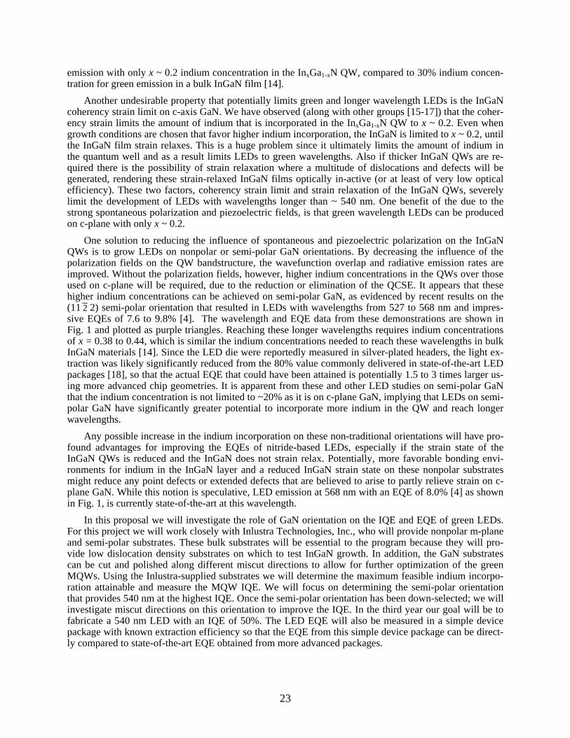
Fig. 1. State-of-the-art external quantum efficiency (EQE) plotted vs. wavelength as of 2009. The data shown in blue and red are from Philips Lumileds and the data in green are from Nichia Chemical Corp. The solid line is the CIE sensitivity of the human eye, while the dashed lines show the EQE trends as a function of wavelength. The open circle is the estimated EQE at 540 nm. The purple trian-gles are for growth on semi-polar GaN substrates [4].
3. PROJECT OBJECTIVES
Despite substantial progress, green nitride-based LEDs are still not as efficient as blue nitride-based or red phosphide-based LEDs [9]. This is clearly shown in Fig. 1, where state-of-the-art external quantum efficiencies (EQEs) are plotted with blue and green symbols for nitride-based LEDs and red circles for phosphide-based LEDs. The dashed lines are extrapolations through these state-of-the-art EQEs for the various wavelengths. Since GaN and InN have bandgaps of 3.4 and 0.7 eV, LEDs with InGaN alloy ac-tive regions should be able to produce all visible wavelengths. However, problems with the growth of these alloys still limit the wavelength region of efficient emission to the UV, blue, and green. The exact reason for the decrease in the EQE as indium is added to the InGaN quantum wells (QWs) for green and longer wavelengths is still not fully understood, however, several factors likely contribute to the decrease in the EQE.
These factors include growth related is-sues that directly affect the InGaN material quality, such as the low growth temperatures and high ammonia fluxes required for indium incorporation. The selection of these growth conditions is driven by necessity to realize higher indium concentration InGaN alloy compositions. One consequence of these con-ditions may be an increase in non-radiative recombination centers in the material, leading to the reduced EQE observed in green wave-length LEDs. Whether or not these non-ideal growth conditions lead to an increase in the number of non-radiative recombination cen-ters must still await further study. However, it may be possible to decrease the density of these defects on other surface orientations or when higher growth temperatures can be used for the InGaN active region.
Only recently, GaN surface orientations other than c-plane have been developed for the growth of InGaN-based LEDs [6]. The main reason for the exclusive focus on the c-plane GaN or the (0001) surface is because this orientation is the easiest to grow on c-plane (and a-plane) sapphire. With the development of AlN and GaN buffer layers schemes [10, 11], use-able GaN films could be fabricated early on, which led to fantastic advances in blue and green LED out-put power and the current revolution in solid-state lighting (SSL).
Regardless of the ease of III-nitride growth on the (0001) surface, there are several undesirable film properties that may ultimately limit the EQE of nitride-based devices. The primary undesired property is the strong spontaneous polarization and piezoelectric fields that act along the growth direction and are due to the strong covalent and ionic bonding and non-centrosymmetric nature of the GaN lattice [12]. For QWs grown along this (0001) direction (i.e. c-axis growth), these fields spatially separate the electron and hole wavefunctions, which decreases their overlap and reduces the radiative emission rate [13]. Due to the poor wavefunction overlap in these polar QW materials, the QWs are typically grown thinner (2-3 nm) to improve radiative emission at the cost of decreasing the emission volume. On the positive side, the piezo-electric field acts to decrease the InGaN QW transition energy due to the quantum confined Stark effect (QCSE). This decrease in the emission energy (red shift) is substantial and allows green wavelengths
23
emission with only x ~ 0.2 indium concentration in the InxGa1-xN QW, compared to 30% indium concen-tration for green emission in a bulk InGaN film [14].
Another undesirable property that potentially limits green and longer wavelength LEDs is the InGaN coherency strain limit on c-axis GaN. We have observed (along with other groups [15-17]) that the coher-ency strain limits the amount of indium that is incorporated in the InxGa1-xN QW to x ~ 0.2. Even when growth conditions are chosen that favor higher indium incorporation, the InGaN is limited to x ~ 0.2, until the InGaN film strain relaxes. This is a huge problem since it ultimately limits the amount of indium in the quantum well and as a result limits LEDs to green wavelengths. Also if thicker InGaN QWs are re-quired there is the possibility of strain relaxation where a multitude of dislocations and defects will be generated, rendering these strain-relaxed InGaN films optically in-active (or at least of very low optical efficiency). These two factors, coherency strain limit and strain relaxation of the InGaN QWs, severely limit the development of LEDs with wavelengths longer than ~ 540 nm. One benefit of the due to the strong spontaneous polarization and piezoelectric fields, is that green wavelength LEDs can be produced on c-plane with only x ~ 0.2.
One solution to reducing the influence of spontaneous and piezoelectric polarization on the InGaN QWs is to grow LEDs on nonpolar or semi-polar GaN orientations. By decreasing the influence of the polarization fields on the QW bandstructure, the wavefunction overlap and radiative emission rates are improved. Without the polarization fields, however, higher indium concentrations in the QWs over those used on c-plane will be required, due to the reduction or elimination of the QCSE. It appears that these higher indium concentrations can be achieved on semi-polar GaN, as evidenced by recent results on the (11 2 2) semi-polar orientation that resulted in LEDs with wavelengths from 527 to 568 nm and impres-sive EQEs of 7.6 to 9.8% [4]. The wavelength and EQE data from these demonstrations are shown in Fig. 1 and plotted as purple triangles. Reaching these longer wavelengths requires indium concentrations of x = 0.38 to 0.44, which is similar the indium concentrations needed to reach these wavelengths in bulk InGaN materials [14]. Since the LED die were reportedly measured in silver-plated headers, the light ex-traction was likely significantly reduced from the 80% value commonly delivered in state-of-the-art LED packages [18], so that the actual EQE that could have been attained is potentially 1.5 to 3 times larger us-ing more advanced chip geometries. It is apparent from these and other LED studies on semi-polar GaN that the indium concentration is not limited to ~20% as it is on c-plane GaN, implying that LEDs on semi-polar GaN have significantly greater potential to incorporate more indium in the QW and reach longer wavelengths.
Any possible increase in the indium incorporation on these non-traditional orientations will have pro-found advantages for improving the EQEs of nitride-based LEDs, especially if the strain state of the InGaN QWs is reduced and the InGaN does not strain relax. Potentially, more favorable bonding envi-ronments for indium in the InGaN layer and a reduced InGaN strain state on these nonpolar substrates might reduce any point defects or extended defects that are believed to arise to partly relieve strain on c-plane GaN. While this notion is speculative, LED emission at 568 nm with an EQE of 8.0% [4] as shown in Fig. 1, is currently state-of-the-art at this wavelength.
In this proposal we will investigate the role of GaN orientation on the IQE and EQE of green LEDs. For this project we will work closely with Inlustra Technologies, Inc., who will provide nonpolar m-plane and semi-polar substrates. These bulk substrates will be essential to the program because they will pro-vide low dislocation density substrates on which to test InGaN growth. In addition, the GaN substrates can be cut and polished along different miscut directions to allow for further optimization of the green MQWs. Using the Inlustra-supplied substrates we will determine the maximum feasible indium incorpo-ration attainable and measure the MQW IQE. We will focus on determining the semi-polar orientation that provides 540 nm at the highest IQE. Once the semi-polar orientation has been down-selected; we will investigate miscut directions on this orientation to improve the IQE. In the third year our goal will be to fabricate a 540 nm LED with an IQE of 50%. The LED EQE will also be measured in a simple device package with known extraction efficiency so that the EQE from this simple device package can be direct-ly compared to state-of-the-art EQE obtained from more advanced packages.

24
This work differs from prior work on nonpolar and semi-polar because a larger number of semi-polar orientations will be systematically investigated along with a larger number of miscuts around these semi-polar orientations. For InGaN MQWs on GaN, our goal is to uncover what semi-polar orientation and miscut delivers the highest IQE at 540 nm and possibly longer wavelengths.

25
Fig. 2. Valence and conduction band diagram for an InGaN quantum well (QW) grown on (a) polar and (b) non-polar GaN. In (a), the distortion of the valence and conductions band is due to the polarization fields, while in (b) the QW is un-distorted because the polarization fields are nor-mal to the plane of the QW. Note the spatial sepa-ration and decreased overlap of the electron and hole wavefunctions in (a) and the alignment and improved overlap in (b).
4. PROJECT BACKGROUND
In the first two sections below, the advantages and limitations of using (0001) or c-plane GaN sub-strates for producing LEDs are discussed. Section A) describes direct effects of polarization and piezoe-lectric fields on MQWs grown on c-plane GaN, while the section B) describes the consequences of the InGaN coherency strain on GaN. The advantages of nonpolar or semi-polar GaN substrates are discussed in section C), along with the potential advantage the reductions in the polarization fields might have for improving InGaN MQW IQEs.
4.1. Effect of spontaneous polarization and piezoelectric fields on InGaN MQWs
One factor that has long been thought to limit the efficiency of green InGaN materials is the strong spontaneous and piezoelectric polarization fields that result along the c-axis direction. These fields result from the non-centrosymmetric wurtzite crystal structure which, along the c-axis direction, does not have point-of-inversion symmetry. Because of this lack of inversion symmetry and the large electronegativity
difference between the N and metal atoms, a sponta-neous polarization develops along the (0001) direc-tion [12]. Because of the strong bonding, the piezoe-lectric coefficients of the AlInGaN alloys are large. The spontaneous and piezoelectric fields induce charges at the hetero-interfaces and distort the band structure when two different AlInGaN alloy composi-tions are in contact with each other [13]. One exam-ple of this effect for nitride-based LEDs is when InGaN QWs are sandwiched between GaN barrier layers. In this example, the polarization difference between the InGaN and GaN layers creates an elec-tronic band structure that is heavily distorted by the ~1 MV/cm polarization field by this structure, as shown in Fig. 2(a) [12]. This distortion of the elec-tron and hole bands decreases the spatial overlap be-tween the electron and hole wavefunctions, thereby decreasing the wavefunction overlap and reducing electron-hole recombination. One way this conse-quence manifests itself for c-plane MQWs is that the QW widths are limited to 2 – 3 nm to maximize the wavefunction overlap. This quantum well thickness is substantially thinner than in similar optical devices in
the other III-V compound semiconductors. It is believed that by nullifying or reducing the spontaneous and piezoelectric polarization fields the electron and hole wavefunction overlap could be improved as shown in Fig. 2(b), resulting in improved quantum yield and efficiency in the nitride-based LEDs. How-ever, because the piezoelectric polarization depends on strain, the polarization-induced reduction in radia-tive recombination rate is larger for longer emission wavelengths (moving towards the green and yellow) where higher-indium-concentration InGaN is grown coherently strained on GaN.
The polarization fields also impact the LED and MQW emission wavelength as well as the stability of the emission wavelength with carrier density. One advantage to LEDs on c-plane GaN is that, the polari-zation-induced fields produce a red shift in the InGaN QW emission wavelength, allowing longer wave-lengths to be achieved at a given alloy composition. For example, green wavelength emission (530 nm) can be achieved in InGaN QWs using indium concentrations of x ~ 0.2, while x ~ 0.3 indium concentra-tions are necessary to achieve 530 nm emission for bulk InGaN films with these same fields [14]. Howev-

26
Fig. 4. (Left) X-ray diffraction rocking curve of a 5 layer green wave-length MQW sample grown on c-plane GaN. The measured scan is shown in red and a dynamic diffraction simulation of the scan is shown in blue. (Right) Reciprocal space map around the (2025) x-ray reflection. Both x-ray scans demonstrate that the InGaN layers are coherently strained to the underlying GaN lattice.
Fig. 3. XRD measurements of the composi-tion of thick InxGa1-xN films grown on GaNat 760 C. Initially coherent films are lim-ited to x=0.20 at high TMIn flow rates;strain relaxation occurs as the film growsthicker, yielding a second layer of highercomposition.
er, this polarization-induced red shift is primarily realized at lower electrical currents and is counteracted at higher current densities by carrier-induced screening of the internal fields. The overall effect is a blue-shift of emission wavelength with increasing current, which is problematic for achieving a color-stable, white light source.
4.2. Influence of coherency strain limit on InGaN films on c-plane GaN
Several groups have reported that lattice-mismatch strain strongly limits the indium composition of InGaN MQWs on GaN templates [15-17]. This strain limit arises because epitax-ial stress alters the vapor-solid thermodynamic equilibrium, lowering the solid-phase epitaxial composition towards the lat-tice-matched condition and away from the gas-phase composi-tion [19, 20]. Fig. 3 shows the growth experiments from our laboratory where the indium composition during the initial stage of InxGa1-xN growth is limited to x ~ 0.2 (blue squares). As the InGaN thickness increases, the InGaN strain relaxes, which allows a near doubling of the indium concentration at the highest indium flow rate. Therefore, under these growth condi-tions the indium incorporation is limited not by the choice of growth conditions but by the coherency strain limit. As previ-ously discussed, the strain relaxed InGaN films contain many defects and a rough surface morphology, making them unsuita-ble for LED applications [21]. Despite the x ~ 0.2 coherency strain limit, green wavelength LEDs are still obtained, because of the red shift induced by the strong polarization forces as dis-cussed in the previous section.
The coherency strain limit also manifests itself for indium incorporation in InGaN MQWs, limiting the indium incorporation to x ~ 0.2. This limit is observed x-ray rocking curve measurements from our
laboratory, shown in Fig. 4 for 5-period InGaN MQWs. In Fig. 4 the x-ray diffraction scan is shown in red and a dynamic dif-fraction simulation of the MQW structure is shown in blue. From the simulation, the indium con-centration is x = 0.195 which is close to the indium coherency strain limit. For the dynamic diffraction simulation shown in Fig. 4, it is assumed that the InGaN QW is coherently strained to the underlying GaN lattice. To the right of the rock-ing curve measurement in Fig. 4 is a reciprocal space map of an InGaN MQW sample that also contained an indium concentra-tion of x ~ 0.2. The fact that the InGaN superlattice satellites have the same K║(x-axis) values

27
Fig. 5. AFM images of c-plane GaN immediately after the growth of (a) the low temperature GaN barrier layer.Successive AFM images are shown after the growth of (b)1; (c) 2; and (d) 3 green MQWs. The InGaN QWs have ~20% indium concentration. All AFM images are 1 m x1 m.
around 4.56 Å-1 as indicated by the red vertical line demonstrates that the InGaN QWs are coherently strained to the underlying GaN lattice.
Although no major bulk relaxation is occurring during typical InGaN QWs on c-plane GaN as meas-ured by x-ray diffraction, we have observed changes in the InGaN step structure. We found that the GaN single-layer step height morphology changes to multiple-layer step heights during InGaN growth [22]. The extent of this change depends on amount of indium incorporated into the InGaN QW [22]. In Fig. 5, the change in the step morphology is illustrated as the number of green LED MQWs increases. In Fig. 5(a), the starting GaN surface is shown, which is composed of single layer height steps. The GaN surface in Fig. 5(a) was imaged after an 11 nm thick low-temperature GaN barrier layer was grown on top of the high-temperature GaN template layer. The image shown in Fig. 5(a) and the image of the starting high temperature GaN layer are identical in appearance, indicating that the lower-temperature GaN growth does not change the overall step morphology.
Conversely, the surface morphology changes after the growth of a single InGaN QW, as shown in Fig. 5(b). For the AFM scan measured after the growth of the single QW shown in Fig. 5(b), as well as after the second and third QWs shown in Figs. 5(c) and 5(d), an indium concentration of x ~ 0.2 was used. It was found that the proportion of multi-layer step heights increased upon MQW growth. Note that there is less change in the AFM images measured after the growth of the second and third MQWs, and when quantified the number of double step height steps approaches a constant value. In other experiments, we find that the degree of increase in the multi-layer step heights is proportional to the indium concentration in the InGaN QW [22]. Therefore, we believe that the change in surface morphology is caused by the slight strain relaxation afforded by the generation of multi-layer InGaN steps. A steady-state step configu-ration arises is due to the competing roughening (InGaN growth) and smoothing mechanisms during the GaN barrier growth. Observation of the natural tendency for InGaN to roughen is important, since a re-cent paper has suggested that InGaN-quantum-well (QW) thickness fluctuations when coupled to the strong piezoelectric-field effects will produce energetic fluctuations strong enough to localize electron-hole pairs [19]. This proposal seems intriguing considering both the tendency for InGaN to roughen natu-rally during growth [20]and the recent atom probe characterization of monolayer thickness fluctuations at the top of QWs due to the roughen InGaN at the InGaN/GaN interface [23]. Even though the multi-layer steps are formed to partly relieve the InGaN lattice strain, the relaxation is extremely small and hence is not observed in x-ray measurements.
Finally, InGaN coherency strain might also be partly relieved through the formation of lattice vacan-cies or defects. Again this type of defect mechanism will only relieve a small fraction of the strain in the InGaN layer. Whether or not these classes of defects are present in InGaN QWs is still an open question. However, if they increase proportionally to the InGaN film stress as more indium is added to the QW and these defects are non-radiative centers, it may explain in a simple way the origin of the decreased IQE observed as the QW wavelength increases. Recently, Yamada et al. have hypothesized that non-radiative centers caused by strain may be a contributing factor that reduces the green and yellow LED efficien-cy[1]. The strain relaxation phenomena on other orientations of GaN may be significantly different than those observed on c-plane GaN.

28
Fig. 7. PL peak wavelength of the LEDs grown on the off-axis substrates along the c-direction from Ref. [1].
Fig. 6. Piezoelectric polarization of an InGaN QW grown pseudomorphically on GaN as a func-tion of crystal orientation. Zero degrees repre-sents c-plane (0001) growth, (11-22) is a semi-polar crystal plane, and m-plane (1-100) is a nonpolar crystal plane. Pz is the polarization per-pendicular to the growth plane (from [6]).
4.3. Advantages of nonpolar and semi-polar oriented GaN for InGaN LEDs
Given these undesirable polarization and strain effects, a significant effort has been expended to de-velop InGaN LEDs on GaN templates with nonpolar (e.g., m-plane (1-100) or a-plane (11-20)) or semi-polar (e.g., (11-22)) crystal orientations. As shown in Fig. 6, moving to these non-traditional crystal orien-tations affords the opportunity to greatly reduce, and even eliminate, polarization effects in wurtzite nitride materials [24, 25]. However, early attempts to achieve nonpolar GaN templates by heteroepitaxial growth on foreign substrates, such as a-plane GaN on r-plane sapphire, resulted in unacceptably high densi-ties of extended defects, such as threading disloca-tions (> 1010 cm-2) and stacking faults (> 105 cm-1) [26]. More recently, the commercial availability of high-quality, free-standing, nonpolar GaN substrates grown by hydride vapor-phase epitaxy (HVPE) have enabled major advances. These substrates are formed by slicing small-area wafers with nonpolar orienta-tion from thick, high-quality, c-plane-oriented sub-strates [27-29]. By employing such m-plane GaN substrates with threading dislocation densities less than 5x106 cm-2, the University of California at Santa Barbara (UCSB) group reported remarkable progress in LED performance: an EQE of 45% at 402 nm, comparable to the best results from polar (c-plane) InGaN LEDs [30].
With these advances, nonpolar InGaN LEDs have reached the material quality where their advantages and limitations can be more clearly examined. As expected from nonpolar LEDs, many reports have con-firmed that the LEDs show improved wavelength stability with increasing current compared to c-plane LEDs [30-32]. And, as mentioned above, efficiencies of the best m-plane InGaN LEDs at near-UV wave-
lengths have met or exceeded those of c-plane LEDs [30]. However, indium incorporation efficiency in nonpolar orientations is reported to be 2-3X less than for c-plane, making it more difficult to reach blue and longer wavelengths [33]. Increased indium incorpora-tion could be achieved by using lower growth temper-atures than those used for c-plane growth, but such an approach is expected to reduce material quality. Therefore, various active region designs, including wide QWs and thick barrier layers, have been em-ployed to achieve longer wavelengths. These efforts have enabled blue (468 nm) LEDs on m-plane GaN substrates with EQEs of 16.8% at 20 mA [33]. The key to increasing the wavelength to 468 nm in these LED structure was to vary the m-plane miscut along the a- and c-directions [1]. As shown in Fig. 7 the PL wavelength only increases when the c-direction is ori-ented to less than -1°. Interestingly, even though simi-lar growth conditions were likely used, the peak wave-

29
length increased due to increased indium incorporation on this wafer miscut, implying that this step direc-tion likely improves indium incorporation. This correlation between wafer miscut and indium incorpo-ration will have a profound influence on optimizing the InGaN QWs for longer wavelengths, especially for this current proposal.
It should be noted that semi-polar LEDs provide an interesting compromise for achieving emission in the green-yellow region. As shown in Fig. 6, the semi-polar (11-22) plane has substantially reduced pie-zoelectric polarization compared to the c-plane, and the indium incorporation efficiency on the (11-22) plane is reported to be comparable to that of c-plane [33]. These factors have enabled the demonstration of (11-22) LEDs at blue, green, and amber wavelengths [34]. Recent performance advances include EQEs of 10.5% at 20 mA in the green region (516 nm) [35] and EQEs as high as 9.5% at 20 mA in the green-yellow region (562 nm) [34]. While the results in the green are not yet competitive with c-plane LEDs, the green-yellow LED performance reportedly surpasses that of any LEDs in this wavelength re-gion, representing an important advance. Ultimately, nonpolar and semi-polar nitrides may play a role in enabling both LEDs and laser diodes in the green-yellow region. Continued improvements in longer wavelength device efficiencies as well as sustained development of larger-area, high-quality, nonpolar substrates [30], may be critical for LED commercial success at these wavelengths.

30
5. DESCRIPTIONS OF PROJECT TASKS
Three tasks are described below from the original proposal with each task encompassing one year. In Section 4, we report on the progress made on each task via the subtasks generated for this program.
5.1. Task 1 – Develop InGaN MQWs on basal or miscut m-plane GaN substrates
In this task our goal is to establish wavelength and IQE limits of QW growth on miscut m-plane GaN bulk substrates. Our target for success in the first year will be to develop MQWs that have emission at 540 nm at an IQE of 20%. Inlustra will deliver 40 nonpolar and 18 semi-polar substrates to Sandia Na-tional Laboratories, along with one time repolishing of 40 substrates.
We will purchase GaN bulk substrates from Inlustra Technology, Inc. for the growth experiments. Some of the previous LED work on nonpolar and semi-polar GaN in the literature was conducted on het-eroepitaxial films grown on sapphire and SiC. Unfortunately, those films often contained too many dislo-cation and stacking fault defects, such that the LEDs had low EQE values despite substantial effort in the growth and fabrication. Inlustra has substantial experience in producing m-plane GaN substrates by slic-ing and polishing c-plane wafer grown using hydride vapor phase epitaxy (HVPE). They are well posi-tioned to provide the starting m-plane on-axis and miscut wafers for the initial phase of the program as well as future semi-polar GaN orientations. They will provide details of the substrate orientation which can be confirmed using Laue x-ray diffraction and they work closely with a company that provides sub-strate polishing. Key to this research will be producing a consistent polished surface and careful meas-urement of the substrate orientation, especially the miscut substrates.
Initial MOCVD growth experiments will focus on developing InGaN MQW growth conditions that provide the maximum incorporation of indium into the QW while maintaining optical efficiency. Growth will be conducted in a Veeco D125 short-jar MOCVD reactor. Growth conditions such as QW growth temperature and ammonia to metalorganic flow rates will be varied, since we have observed these growth conditions to have the most influence on indium incorporation on c-plane GaN. A special substrate holder will need to be designed hold the smaller size nonpolar and semi-polar substrates. For each growth a c-plane GaN wafer will also be included so that the relative difference between the nonpolar or semi-polar and c-plane substrates can be determined. Also, to increase the IQE of blue and green MQWs on c-plane GaN, we have used dilute indium concentration InGaN layers (commonly referred to as underlayers) un-der the MQWs. These InGaN underlayers will also be tried on the m-plane and semi-polar orientations to determine if they also improve the IQE. The growth is routinely monitored using optical reflectance, and the surface temperature of the GaN substrate can be monitored using a novel 400 nm emissivity correct-ing pyrometer developed at Sandia, due to the opaqueness of the GaN film at this wavelength [36].
To characterize the samples, x-ray diffraction, photoluminescence (PL), Hall Effect measurement, and a suite of more specialized techniques will be used. The MQW structure can be verified using x-ray diffraction as illustrated in Fig. 4. To our knowledge there is no currently available commercial x-ray dif-fraction software package to provide a dynamical diffraction fit to the x-ray scan on nonpolar or semi-polar GaN, so initial analysis of the indium concentration may be limited to determining the average indi-um content in the layers. Knowing the average indium content along with the QW+barrier thickness and growth times should allow for a good estimate of the MQW growth parameters. Determining the indium compositions in a more rigorous way from x-ray diffraction will not be as straightforward as it is on c-plane GaN since commercial computer programs to simulate the MQW scan are not yet available. Instead the determination of the MQW parameter may require separate measurement of three x-ray diffraction peaks and solving the non-isotropic strain matrix for the given substrate orientation to determine the InGaN lattice parameters and strain state of the InGaN MQWs.
The indium content can also be estimated from the PL wavelength with knowledge of the degree of polarization and piezoelectric forces on a particular growth plane. Variable temperature PL measurements

31
will be used to determine the IQE by comparing the room temperature PL emission intensity to the PL emission intensity at 4 K. For the 4K PL measurement it is commonly assumed that the non-radiative component is fully quenched such that only the radiative component emits and the IQE is assumed to be unity. As the temperature is increased to room temperature the non-radiative component increases and the IQE is calculated from the normalized decreased PL intensity. These temperature dependent PL meas-urements will be conducted over a range of excitation powers, and will use selective pumping of QW lay-ers, to ensure proper interpretation of the IQE results.
The surface morphology will be imaged using AFM and SEM. AFM measurements will initially be used to determine the quality of the surface polish; after GaN growth the surface morphology can be ex-amined for growth structures that might arise due to the polishing damage. AFM images can also be used to detect possible changes in the InGaN morphology after the MQW growth, as illustrated in Fig. 5.
After the initial basal m-plane growth experiments, vicinal or miscut m-plane substrates will be ex-plored. One option for the first year research will be to quickly move to semi-polar oriented substrates if 540 nm wavelengths are not reached on the miscut m-plane substrates. In the first year we expect to ob-tain a total of 40 m-plane substrates, and 18 semi-polar substrates. After thorough characterization of the individual MOCVD growth runs, ~ 40 wafers will be repolished at a nominal cost. We emphasize that our agreement with Inlustra will allow for a range of nonpolar and semi-polar substrate orientations com-bined with a level of substrate quality not typically available in previously reported studies.
5.2. Task 2 – Develop of InGaN MQWs on semi-polar GaN substrates (3 different orientations)
The second task will take place in the second year of the project. During the second task, we will work toward down selecting semi-polar orientations give the highest MQW IQE and the longest wave-lengths. The target for success is 540 nm with 35% IQE. Inlustra will deliver similar quantities of GaN substrates in the second year as those delivered in the first year.
Our first choices for semi-polar orientations will be the (10-11) which are the hexagonal pyramidal facets on the nanopillars shown in Fig. 8 that produced a high IQE and also the (11-22) which was used by Fellows et al. for producing high EQE LEDs [4]. These orientations are the most stable growth orien-tations during GaN growth and are the slow and fast growth orientations observed in kinetic Wulff plots described by Du et al. [37]. Other GaN orientations described in Ref. [37] could have even higher growth rates and might provide even higher indium incorporation. Two possible orientations lie between (10-11) and m-plane orientations and the (11-22) and a-plane orientations [37].
For these semi-polar substrate orientations, the maximum indium incorporation will be determined in a series of growth experiments where high indium fluxes are used at nominally high temperatures. Under these growth conditions the indium concentration is determined primarily by the indium desorption rate. Therefore the growth temperature will be an important factor in determining the indium incorporation in the QW. In preliminary research of InGaN QW growth on nanopillars, a higher InGaN QW growth tem-perature was chosen to reach blue wavelengths; however, a substantially larger indium concentration was incorporated leading to the observed 575 nm emission on the (10-11) regions of the nanopillars. This im-plies that the (10-11) orientation may provide a better bonding environment for indium incorporation compared to the normal c-plane surface. This effect is also suggested from the data of Yamata et al. [1], where a slight miscut of the m-plane GaN resulted in a substantial increase in the indium concentration and resultant wavelength. Again our major focus will be on obtaining the maximum indium concentra-tions in the MQWs to reach to longest wavelengths. Once these maximum indium concentrations are de-termined, we will optimize growth conditions to improve the IQE of 540 nm MQWs.
Since in the third year of this program we will develop LEDs to measure the EQE of our brightest InGaN MQWs, we will begin developing p-type doping on nonpolar and semi-polar orientations of GaN. We have found different growth conditions are necessary for good p-type doping, compared to the growth conditions used for GaN and InGaN growth. We will use Hall Effect Measurements to determine the hole

32
concentrations on top of an undoped GaN layer on the Inlustra substrates. In addition, we can use a capac-itance-voltage measurement technique to profile the hole concentration into the material. In addition, PL can be used to qualitatively assess the p-type material. We can compare PL signatures that we commonly observe in our best p-type material on c-plane GaN to the p-type material we develop on the nonpolar and semi-polar orientation substrates.
5.3. Task 3 – Optimize InGaN MQWs on miscut semi-polar GaN sub-strates
In the third year our goal will be to produce an LED on semi-polar GaN. The EQE of the LED will be measured in a standard package and the light extraction will be estimated based on the package design. We will target a 540 nm LED with an EQE of 40%. Inlustra will deliver similar quantities of GaN sub-strates in the third year 3 as those delivered in the first year.
To reach the goal of delivering a 540 nm LED with an EQE of 40%, we will pick the semi-polar ori-entation that has the highest IQE and we will develop miscut wafers to further optimize the IQE. Similar to the first and second years, we will determine the maximum indium concentration obtainable and then focus on optimizing emission at 540 nm with high IQE. Again, we will rely heavily on x-ray diffraction and PL measurements to determine indium concentration and IQE.
Beginning in the second half of the third year, we will develop semi-polar LEDs. Once the appropri-ate doping levels are attained and the QW structure is developed, we will grow full LED structures using optimized growth conditions. LEDs will be based on single or multiple QW designs grown on n-type GaN nonpolar or semi-polar substrates. On top of the QWs, a p-type AlGaN electron block layer will be grown along with a final p-GaN contact layer. For rapid turnaround, “quick-test” LEDs using In-metal contacts will be fabricated, and on-wafer testing will be performed to get an early indication of the per-formance of the LED wafer. Promising LEDs selected from these “quick-test” surveys will be fabricated using our standard process for top-emitting devices employing a semi-transparent NiO p-contact. We also have a flip-chip LED process for a range of device sizes (200 m to 1 mm on a side) that can be em-ployed in this project, as needed. Processed LED structures will be diced into die and mounted on stand-ard TO-type headers for testing. LED testing will include L-I-V (light output, current, voltage) measure-ments using both CW and pulsed current and will employ a calibrated integrating sphere to obtain quanti-tative values of LED external quantum efficiency. LED internal quantum efficiency will then be estimat-ed from knowledge of the extraction efficiency of the particular LED chip geometry.

33
Fig. 8. X-ray rocking curve diffraction of the (10-10) reflection along the c-axis for the previous and new m-plane bulk samples.
6. WORK PERFORMED UNDER EACH PROJECT SUBTASK
In this section we will report on the work done under each of the Subtasks. We note that the program had a delay before starting and an initial delay in delivery of the first sample set. For this project we were notified the award for this proposal on August 25th, 2009. After some delay the funds reached Sandia Na-tional Laboratories on January 6th, 2010 and the program officially started January 15th of 2010. After the proposal award, a purchase order was initiated to purchase substrates from Inlustra. The purchase contact took 2 ½ months to put in place and was finally awarded March 26th. This delay in getting the purchase contact in place delayed the delivery of the first set of m-plane substrates until late June. Prior to the June delivery of m-plane substrates, Inlustra delivered m-plane sample substrates for initiation of growth ex-periments at Sandia. These sample m-plane substrates were subprime but allowed initial experiments of indium incorporation and multi-quantum well (MQW) growth. After the initial delay in the delivery of m-plane substrates, Inlustra increased the delivery schedule and m-plane substrates were delivered on June 30th and September 29th, leading to accelerated growth research reported later in this section. Semi-polar GaN substrates with a (10-13) orientation were delivered on September 29th, November 11th, and Decem-ber 2nd.
6.1. Subtask 1.1: Develop epi-ready m-plane polished crystals at Inlus-tra and deliver to Sandia.
In the first year Inlustra delivered to Sandia a total of 56 m-plane (1-100) and 43 semi-polar (10-13) substrates. The substrates were ~ 5 mm x 10 mm in size and using a modified sapphire carrier cutout we were able to place them in the center of the growth zone on our 2” wafer carrier cutouts. Many of the crystals contained cracks and visible defects. From x-ray diffraction studies several different mosaic peaks were some-times observed as discussed later. The surface polish by eye appeared smooth and under microscope examination the sur-face appeared to be composed of distinct domains. From the first to the second delivery of m-plane substrates there was improvement in the crystal quality. After growth, the surface many times appear rough under the microscope.
To demonstrate the improvement in the m-plane substrates delivered by Inlustra, x-ray rocking curve scans are shown in Fig. 8 for films delivered in June, 2010 (blue curve) and later
in September (red curve). The scans shown in Fig. 8 are for the (10-10) reflection. The almost factor of two increase in the x-ray intensity and decreased linewidth indicate better crystalline quality of m-plane samples delivered in September. Further crystal quality improvement is expected for both the m-plane and semi-polar substrates will be necessary in order for x-ray diffraction determination of indium concen-trations in MQW and thin InGaN films.
6.2. Subtask 1.2: Determine maximu m indium composition in MQWs on m-plane GaN.
Initial MOCVD growth experiments focused on developing InGaN MQW growth conditions that provide the maximum incorporation of indium into the QW. Growth conditions such as QW growth tem-perature were varied because this growth condition has been found to have the most influence on indium incorporation for InGaN MQWs grown on c-plane GaN. A special substrate holder was designed to hold

34
the smaller size nonpolar and semi-polar substrates. For each growth, a c-plane GaN wafer was also in-cluded so that the relative difference between the nonpolar or semi-polar and c-plane substrates can be determined. To characterize the samples, x-ray diffraction, photoluminescence (PL), Hall Effect meas-urement, and more specialized techniques were used. The indium content was estimated from the PL wavelength based of the degree of polarization and piezoelectric forces on a particular growth plane. The IQE of the MQWs was measured using variable-temperature PL measurements. The surface morphology was imaged using AFM and SEM.
After the delivery of the first m-plane substrates in April, initial MOCVD growth experiments fo-cused on developing growth conditions that provide the maximum incorporation of indium into the QW. Growth conditions such as QW growth temperature, indium flow rate, and QW growth time will be varied first, since these growth conditions have the most influence on indium incorporation for c-plane InGaN MQWs. For each growth, a c-plane GaN substrate was co-loaded and grown on for comparison. After growth the samples were characterized using photoluminescence (PL) and x-ray diffraction (XRD) when feasible, Hall Effect measurements for p-type GaN, and more specialized techniques such as AFM. The indium concentration was best estimated from the PL wavelength with the knowledge that the piezoelec-tric forces are absent on the m-plane substrates and are small on the semi-polar orientations close to the m-plane. The internal quantum efficiency (IQE) of the MQWs will be measured using variable-temperature PL measurements.
6.2.1. Sample holder development
Specialized sapphire sample holders, previously designed for growth on ¼ of a 2” wafers were evalu-ated for the 5mm x 10 mm sized GaN substrates. These wafer holders were made from 2” sapphire wafers with a ¼ wafer cutout in the middle of the wafer. Initially, these wafer cutout holders were tested using 12x12 mm2 m-plane SiC wafers on which AlN was grown on top. For each of 3 growth runs, either two or three of the SiC wafers or their holders were loaded into the MOCVD reactor. During these test growths, none of the SiC substrates were lost or mechanically damaged as a result of the high-speed plat-en rotation required for crystal growth. Later growth on the Inlustra bulk sized sample was also successful and to date not a single bulk 5 mm x 10 mm sample has been lost in the MOCVD reactor even when us-ing rotation speeds of up to 1200 rpm.
6.2.2. Development of XRD characterization methods for m-plane III-nitride hetero-structures
One of the best characterization methods for the evaluation of thin film structures and composition is x-ray diffraction (XRD). As common practice, we routinely use XRD to determine MQW and LED structure of c-plane sapphire. After the XRD scan is measured, a dynamical diffraction analysis package from Phillips is used (X’Pert Epitaxy) to determine the MQW layer thicknesses and the indium concen-trations. Good dynamical diffraction analysis fits can also be used on LED structures allowing thicknesses to be obtained for the AlGaN electron blocking layer and the p-type GaN contact layer. Unfortunately, we do not have a similar software package for fitting the-se structures on m-plane, a-plane or other semi-polar planes. Also, communications with several other XRD manufacturers yielded little information on
Fig. 9. Diagrams of strained and unstrained hexagonal unit cells resulting from III-nitride heteroepitaxy on m-plane or a-plane surfaces. The unit cell is view along the c axis with the basal plane shown in plan-view; the upper drawings show strained epilayers placed under in-plane compression.

35
Fig. 10. Schematic diffraction pattern of a III-nitride crystal viewed along the <0001> zone axis. The diffraction-pattern indexing corre-sponds to the primitive-cell orientation super-imposed at the center of the figure.
methods used for fitting InGaN-based structures on these other non-standard GaN planes, and even if the software was available from other vendors, the software would not be sold unless XRD equipment was also purchased. Also, before this program began, surveys of the literature showed little information on XRD evaluation of InGaN-based structures on planes other than c-plane, suggesting careful consideration of the XRD signatures of InGaN structures on these non-standard GaN planes was desperately needed.
In March of 2010, work began on modeling, experimental procedures, and basic data needed to ena-ble XRD measurements of lattice parameters, strains, compositions, and dislocation densities for III-nitride heterolayers grown on the m-plane. Initial XRD scanning procedures were assessed using the m-plane AlN/SiC heterostructures grown in mechanical stability described above (XRD procedures for m-plane GaN will be similar to those for m-plane AlN, with only minor adjustments for lattice parameter). Symmetric (1010) and (3030) and asymmetric (1230) and (1011) reflections for m-plane AlN/SiC were successfully measured using a variety of rocking-curve and radial () scanning techniques. Equations needed to extract strain and composition from m-plane XRD data are presently in development and will be tested using the data acquired from our m-plane AlN/SiC wafers.
In April, work was completed to derive equations needed to interpret x-ray diffraction measurements of strain and composition in m-plane III-nitride alloys grown on m-plane GaN, AlN, or SiC substrates. For strained m-planes III-nitride heterolayers on m-plane GaN, the hexagonal crystal structure changes to an orthorhombic crystal structure because of the anisotropic in-plane biaxial strains that are applied dur-ing heteroepitaxy. To avoid mixed-index notational complications resulting from combining the ortho-rhombic epilayer with the hexagonal substrate, we developed a special “pseudo-hexagonal” equation for the d-spacing of orthorhombic crystals that uses hexagonal-type Miller indices compatible with the sub-strate. Resulting equations allow straightforward determination of the strained lattice parameters of the m-plane epilayer given a suitable set of XRD 2θ measurements.
Once an m-plane epilayer’s strained lattice parameters are known from XRD, additional modeling equations are needed to compute the layer’s composition, unstrained lattice parame-ters, and elastic strain. Using appropriate elasticity theory, Vegard’s law for the III-nitride-alloy lattice parameters, and the definition of strain, suitable m-plane equations have been successfully derived.
Our first test made use of a previously reported growth of 250-nm-thick m-plane AlN on m-plane SiC. To determine both the in-plane strains (xx and zz in Fig. 9) and the compo-sition of the strained epilayer, a minimum of three x-ray dif-fraction reflections must be used. For our test we used (-22.0), (-13.0), and (-22.2) reflections to measure corresponding 2 values for the epilayer; two of the selected reflections are shown in Fig. 10, with the third reflection lying out of the plane of the figure. Given the measured 2 values, interplanar spacings from Bragg’s law and strained unit-cell lattice pa-rameters (a, c, & were calculated using our recently derived pseudo-hexagonal d-spacing equation, which is based on the specific unit-cell orientation shown at the center of Fig. 10. Using an additional quadratic equation in the composition,
which was derived from elasticity theory considerations, Vegard’s law, and the strain definitions shown in Fig. 9, we then calculated the epilayer composition (x), the unstrained lattice parameters (a0 & c0), and the epilayer strain state that are self-consistent with the XRD measurements.
The measured AlN mole fraction, x=1.004, is consistent to within a small experimental error with the fact that the test layer is pure AlN. The theoretically expected pseudomorphic coherency strains for AlN on m-plane 6H-SiC are xx=-0.00996 and zz=0.01203. Since the measured strain along <0001>, zz=0.01223, is nearly identical to the expected pseudomorphic strain, we can conclude that the as-grown

36
Fig. 11. Facets of GaN that are included in the kinetic model.
Table I. Summary of XRD measurements of the strain and composition of m-plane and c-plane InGaN/GaN heterostructures grown to a thickness of ~ 500 nm.
AlN layer is completely unrelaxed in this direction. In contrast, the measured strain along the orthogonal <11-20> direction, xx=-0.00244, is much smaller in magnitude than the pseudomorphic strain for this direction, and in fact, the strain is 75% relaxed along this direction. This partial relaxation of strain along only one of the two orthogonal in-plane directions is expected because of the highly anisotropic crystal structure of the m-plane growth surface.
Since initial evaluation of the indium incorporation on 200 nm thick InGaN films on m-plane GaN provided difficult, a second set of samples InGaN samples grown to 500-nm-thick were investigated. These thicker heterostructures enable more direct XRD measurements of composition and strain than is possible for thinner MQWs. M-plane and c-plane sample pairs were concurrently grown using three dif-ferent combinations of indium-precursor flow rate and growth temperature. The three as-grown sample pairs (DNZ03052, DNZ03053, & DNZ03054) are being examined by XRD to determine the composition and strain state of the resulting InGaN layers.
Measurements for sample DNZ03052 have been completed and results appear in Table I below. For the analysis of the indium composition and strain state on m-plane GaN, we used the procedure described in June’s, 2010 monthly report. As seen in the table, both the m-plane and c-plane samples from run DNZ03052 are partially strain relaxed, with the m-plane sample showing substantially less strain relaxa-tion than the c-plane sample. The different degrees of strain relaxation are due to the different amounts of indium that are incorporated on the two planes and the resulting epitaxial strain available to drive relaxa-tion processes. The indium composition of the m-plane sample, x=0.057, is substantially less than that of the c-plane sample, x=0.123. This reduced indium incorporation on the m-plane agrees with some previ-ous InGaN MQW studies [38].
However, this result of lower indium concentration on the m-plane compared to the c-plane stands in contrast with some of our MQW growths (report from Aug. 2010) where we inferred from photolumines-cence experiments that similar indium concentrations must have been incorporated into the MQWs on the c- and m-plane substrates. These similar indium concentrations could be inferred from the PL wave-lengths, where the difference in the PL wavelengths could be accounted for due to the presence of the quantum confined Stark-effect (QCSE) on the c-plane MQWs and its absence on the m-plane MQWs. In several cases more indium must have been incorporated into the m-plane MQWs since the PL wave-lengths were similar on both the c- and m-plane substrates. Depending on growth conditions, we previ-ously observed an increase in the indium composition once the InGaN film strain relaxed on c-plane sub-strates. Clearly, developing the equations for m-plane required substantial work and a full understanding of the indium incorporation on the semi-polar planes will be even more difficult. Because measurement of these materials were hampered by a large spread in peakwidth due sample mosaic, we were unable to further develop the diffraction the-ory necessary to quantify indium in thick InGaN films on semi-polar films.
6.2.3. Development of nonpolar and semi-polar GaN growth kinetics
The polycrystalline morphology evolution observed in growth of non-polar and semi-polar GaN is much more complex than that for conventional c-plane growth, due to the lower symmetry of these planes. As part of this project we are developing a computer

37
Fig. 12. XRD ω-2θ scans of the InGaN MQWs grown on c- and m-plane substrates.
modeling capability to describe the growth and coalescence during non-polar and semi-polar GaN/InGaN MOCVD. The goal of the modeling is to help us understand, control, and manipulate nucleation and growth to obtain better material quality, and ultimately more efficient LED performance.
During the growth of GaN grains, the "outward growth" all of the geometric features are convex. Thus, it turns out that the fastest-growing crystal facets grow to extinction and disappear, leaving behind only the slowest-growing facets. Fig. 11 shows an example output of the code we worked on. The many different crystal planes present in a-plane GaN are illustrated. The code can handle any arbitrary number of crystal facets and orientations (for example, for c-plane, non-polar, or semi-polar orientations).
We have written a graphical post-processor for the model using the IDL software. This capability lets us visualize “movies” of the crystal morphology evolution to quickly test the simulations and to gain a better physical understanding of the facet growth. Our goal is to extend the modeling capabilities to simu-late growth of concave features that occur when isolated crystal facets, for example GaN nuclei during initial growth, collide with one another. We have found that our current growth algorithm is not readily extensible to concave features. However, a more general algorithm described in [39] should be able to handle such concave shapes.
6.2.4. MOCVD growth on m-plane GaN substrates from Inlustra
Due to initial delays in getting the contact in place for substrate purchases, Inlustra sent Sandia five existing m-plane GaN substrates in April 2010, to begin MOCVD growth experiments. Our goal during these initial studies was to determine growth conditions that allow for stable and smooth m-plane facet growth. For these initial growth runs, one micron of GaN was grown at pressures of 75 or 500 torr at V/III ratios of 1400 or 100. AFM images of the surface morphology taken before and after growth show similar morphology, suggesting at least to first order the GaN growth conditions are stable on these sam-ples. After the GaN homoepitaxial growth, two different samples were grow, one with a thick InGaN lay-er and one with an InGaN multiple quantum well. XRD of the thick InGaN layer showed a distinctive
peak due to the InGaN layer. For these m-plane growths, the GaN 2θ XRD peak occurred at 32.4° in close agreement with the expected 2θ angle for m-plane GaN. The InGaN 2θ XRD peak occurred at 31.1°, suggesting an indium composi-tion in the range of 20% based on a rough estimate from a comparable peak shift for co-herently strained InGaN on c-plane GaN. For the second InGaN MQW sample, an m-
plane GaN bulk substrate and a c-plane GaN template were co-loaded into the MOCVD reactor. The MQW growth was preceded by a dilute indium concentration InGaN underlayer followed by a MQW that targeted wavelengths near 520 nm. The XRD scans for both MQW structures are shown in Fig. 12. In both scans, the superlattice peaks due to the InGaN/GaN QWs are clearly observable. Dynamic diffrac-tion analysis fits of the c-plane MQW give 3.2 nm thick QWs with an indium concentration of 20% sur-rounded by 10.2 nm thick GaN barriers. A similar periodicity is observed for the MQWs on the m-plane sample suggesting a similar QW structure. The photoluminescence (PL) scans for both samples are shown in Fig. 13 and show similar PL wavelengths; however, the intensity is lower for the MQWs on the m-plane. The similarity in the PL wavelengths and the lower intensity of the emission on the m-plane sub-strates are likely due to the non-ideal, somewhat faceted m-plane substrate. Since the quantum confined Stark effect should not be operative on the m-plane, shorter wavelengths closer to 475 nm would be ex-

38
Fig. 13. Photoluminescence scans of the InGaN MQWs grown on both c-plane and m-plane GaN substrates.
Fig. 14. XRD rocking curve measurements of InGaN Fig. 15. Same as Fig. 2 except for a faster QW MQWs on c-plane (blue) and m-plane (red) GaN surfaces growth rate and a growth temperature of 760 °C. for a QW growth temperature of 740 °C.
pected for ~20% indium concentration QWs on m-plane. Instead, the longer wavelength is likely the re-sult of ~25 % indium incorporation on this potentially more faceted m-plane sample.
In late June of 2010, the first set of m-plane GaN substrates arrived at Sandia. Growth of additional InGaN MQWs was commenced to study indium incorporation and resultant wavelength emission on the m-plane and co-loaded c-plane GaN. For these studies, the MQWs were grown at a pressure of 300 torr using 15 SLM NH3 and 10 SLM N2. Growth temperatures ranged from 720 to 760 ºC and resulted in wavelengths from 442 to 550 nm on c-plane and 432 to 530 on m-plane as the QW growth temperature decreased. In all cases the MQWs on c-plane were longer in wavelength than on m-plane with the longer wavelengths observed on c-plane due to the presence of the quantum confined Stark-effect on the c-plane its absence on the m-plane. The PL intensity was in general larger on the c-plane MQWs compared to the m-plane MQWs.
Comparisons of the XRD structure for c- and m-plane MQWs are shown in Figs. 14 and 15. For the samples shown in Fig. 14, the quantum well growth temperature was 740 °C with a QW growth time of 1.2 min. A similar perio-dicity of the InGaN superlattice peaks is observed between the c-plane and m-plane samples with the m-plane superlat-tice peaks decreasing in intensity and broadening more strongly as ω decreases, possibly indicating sample inho-mogeneity. From this analysis similar PL wavelengths were obtained for both the c- and m-plane MQW samples sug-gesting the possibility of increased indium on the m-plane compared to the c-plane MQWs. The increased indium on the m-plane could be due to faceting during growth or the large mosaic of the crystal.
For the MQWs shown in Fig. 15, the QW growth rate was increased by a factor of 3.3 times and the QW was grown at a temperature of 760 °C. These two growth changes were made to increase the indium incorpo-ration and maintain a higher growth temperature for better quality InGaN. For this set of samples the in-dium incorporation was measured to be ~17.5 % for the c-plane sample with a QW thickness of 2.8 nm. Similar to Fig. 14 the m-plane InGaN superlattice peaks occur at similar intervals to the c-plane InGaN superlattice peaks. Quick PL evaluation of the these MQWs using a 325 nm HeCd laser resulted in similar wavelengths for both samples, again indicating that the m-plane sample might actually contain more indi-um compared to the c-plane sample. Using these faster QW growth rate conditions we were able to
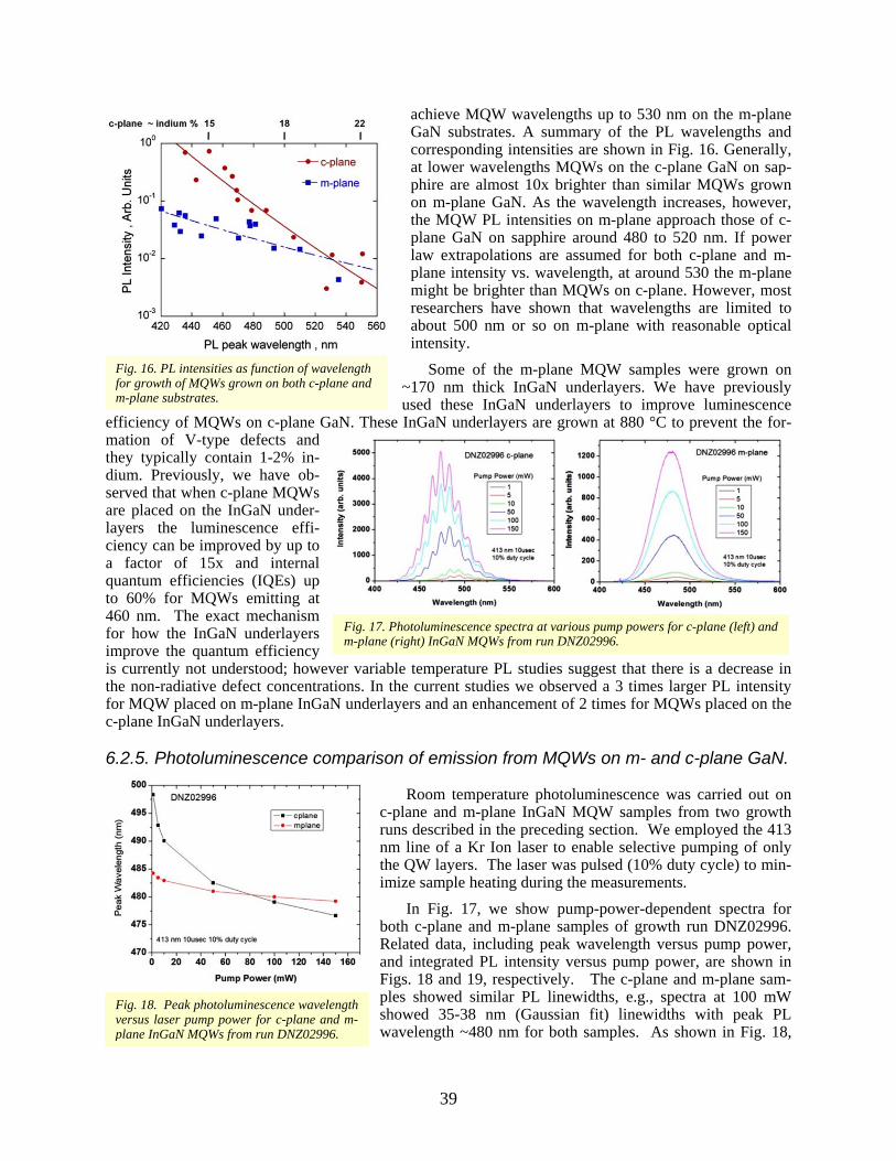
39
Fig. 17. Photoluminescence spectra at various pump powers for c-plane (left) and m-plane (right) InGaN MQWs from run DNZ02996.
Fig. 16. PL intensities as function of wavelength for growth of MQWs grown on both c-plane and m-plane substrates.
achieve MQW wavelengths up to 530 nm on the m-plane GaN substrates. A summary of the PL wavelengths and corresponding intensities are shown in Fig. 16. Generally, at lower wavelengths MQWs on the c-plane GaN on sap-phire are almost 10x brighter than similar MQWs grown on m-plane GaN. As the wavelength increases, however, the MQW PL intensities on m-plane approach those of c-plane GaN on sapphire around 480 to 520 nm. If power law extrapolations are assumed for both c-plane and m-plane intensity vs. wavelength, at around 530 the m-plane might be brighter than MQWs on c-plane. However, most researchers have shown that wavelengths are limited to about 500 nm or so on m-plane with reasonable optical intensity.
Some of the m-plane MQW samples were grown on ~170 nm thick InGaN underlayers. We have previously used these InGaN underlayers to improve luminescence
efficiency of MQWs on c-plane GaN. These InGaN underlayers are grown at 880 °C to prevent the for-mation of V-type defects and they typically contain 1-2% in-dium. Previously, we have ob-served that when c-plane MQWs are placed on the InGaN under-layers the luminescence effi-ciency can be improved by up to a factor of 15x and internal quantum efficiencies (IQEs) up to 60% for MQWs emitting at 460 nm. The exact mechanism for how the InGaN underlayers improve the quantum efficiency is currently not understood; however variable temperature PL studies suggest that there is a decrease in the non-radiative defect concentrations. In the current studies we observed a 3 times larger PL intensity for MQW placed on m-plane InGaN underlayers and an enhancement of 2 times for MQWs placed on the c-plane InGaN underlayers.
6.2.5. Photoluminescence comparison of emission from MQWs on m- and c-plane GaN.
Room temperature photoluminescence was carried out on c-plane and m-plane InGaN MQW samples from two growth runs described in the preceding section. We employed the 413 nm line of a Kr Ion laser to enable selective pumping of only the QW layers. The laser was pulsed (10% duty cycle) to min-imize sample heating during the measurements.
In Fig. 17, we show pump-power-dependent spectra for both c-plane and m-plane samples of growth run DNZ02996. Related data, including peak wavelength versus pump power, and integrated PL intensity versus pump power, are shown in Figs. 18 and 19, respectively. The c-plane and m-plane sam-ples showed similar PL linewidths, e.g., spectra at 100 mW showed 35-38 nm (Gaussian fit) linewidths with peak PL wavelength ~480 nm for both samples. As shown in Fig. 18,
Fig. 18. Peak photoluminescence wavelength versus laser pump power for c-plane and m-plane InGaN MQWs from run DNZ02996.

40
the m-plane sample showed significantly reduced peak wavelength shift with pump power. This characteristic is expected of nonpolar QWs due to the lack of internal polar-ization fields. We see in Fig. 19 that the c-plane sample has, at most, ~3.5X higher integrated PL intensity. We consider this to be a promising result given that this data was measured in the early stages of the program.
Similar PL studies were performed on InGaN QWs grown at lower growth temperature resulting in higher in-dium content (run DNZ02997). In Fig. 19, we show pow-er dependent PL spectra for c-plane and m-plane samples. Without much growth optimization, we found that moving to higher indium significantly degrades the luminescence performance of the m-plane MQWs compared to c-plane MQWs. We observe linewidth broadening and the devel-opment of a long wavelength tail in the m-plane PL spectra
with integrated PL intensity up to 13X lower than the c-plane sample. We note, however, the wavelength stability with pump power is much improved compared to c-plane, as was seen for the shorter wavelength DNZ02996 m-plane sample.
6.2.6. Increasing QW thickness on m-plane and c-plane substrates
Since brighter QWs should be obtained by using a larg-er volume of InGaN, MQWs were grown with thicknesses from 1.7 to 7.0 nm. It is well established that thinner InGaN QWs are necessary on c-plane GaN because the strong po-larization fields decrease the electron/hole wavefunction overlap as the thickness of the QW increases. Unlike on c-plane, the QW thickness on m-plane will not be influenced by the polarization fields and therefore the MQW can be grown substantially thicker to increase the recombination volume, thereby increasing the light emission intensity.
XRD analysis of the indium concentration and QW thickness are shown in Fig. 20 for the MQWs growth on c-plane GaN templates. These QW parameters are obtained from the dynamic diffraction fits to the ω/2θ radial diffrac-tion scans. As expected in Fig. 20, the QW thickness in-creases linearly with the QW growth time.
Also, the indium concentration in the QWs is relatively constant (between x = 0.17 and 0.18) except for the thin-nest QW which has x = 0.16. The rea-son for the decrease in the decreased indium concentration as the QW thick-ness decreases is due to not reaching the full alloy concentration before the termination of the QW growth. For the-se QW the growth time of the QW con-tinues after the indium flow is shut off and surface indium is further incorpo-rated into the QWs since a GaN cap layer is grown at the QW growth tem-
Fig. 20. X-ray diffraction measurement of the indium concentration and QW thickness vs. the QW growth time
Fig. 21: Room temperature PL of c-plane and m-plane MQW structures with different QW growth times. Figure label includes the QW width that is measured by XRD on the c-plane wafer.
Fig. 19. Integrated PL intensity versus laser pump power for c-plane and m-plane InGaN MQWs from run DNZ02996.
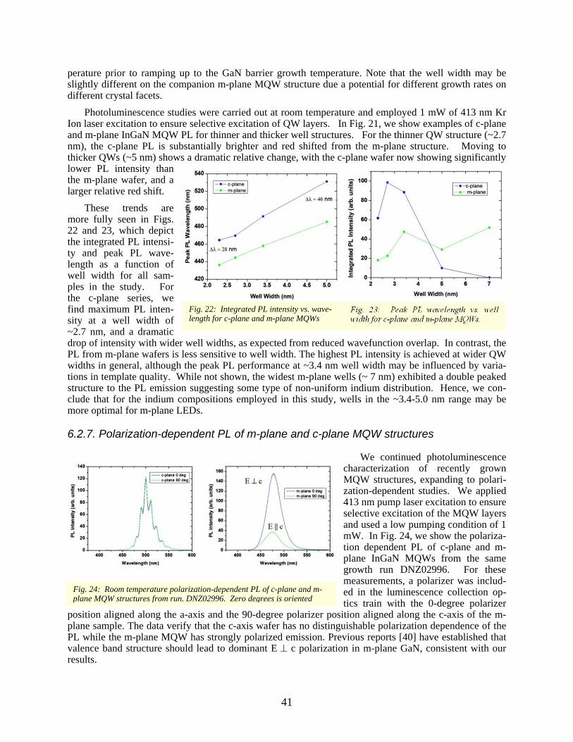
41
perature prior to ramping up to the GaN barrier growth temperature. Note that the well width may be slightly different on the companion m-plane MQW structure due a potential for different growth rates on different crystal facets.
Photoluminescence studies were carried out at room temperature and employed 1 mW of 413 nm Kr Ion laser excitation to ensure selective excitation of QW layers. In Fig. 21, we show examples of c-plane and m-plane InGaN MQW PL for thinner and thicker well structures. For the thinner QW structure (~2.7 nm), the c-plane PL is substantially brighter and red shifted from the m-plane structure. Moving to thicker QWs (~5 nm) shows a dramatic relative change, with the c-plane wafer now showing significantly lower PL intensity than the m-plane wafer, and a larger relative red shift.
These trends are more fully seen in Figs. 22 and 23, which depict the integrated PL intensi-ty and peak PL wave-length as a function of well width for all sam-ples in the study. For the c-plane series, we find maximum PL inten-sity at a well width of ~2.7 nm, and a dramatic drop of intensity with wider well widths, as expected from reduced wavefunction overlap. In contrast, the PL from m-plane wafers is less sensitive to well width. The highest PL intensity is achieved at wider QW widths in general, although the peak PL performance at ~3.4 nm well width may be influenced by varia-tions in template quality. While not shown, the widest m-plane wells (~ 7 nm) exhibited a double peaked structure to the PL emission suggesting some type of non-uniform indium distribution. Hence, we con-clude that for the indium compositions employed in this study, wells in the ~3.4-5.0 nm range may be more optimal for m-plane LEDs.
6.2.7. Polarization-dependent PL of m-plane and c-plane MQW structures
We continued photoluminescence characterization of recently grown MQW structures, expanding to polari-zation-dependent studies. We applied 413 nm pump laser excitation to ensure selective excitation of the MQW layers and used a low pumping condition of 1 mW. In Fig. 24, we show the polariza-tion dependent PL of c-plane and m-plane InGaN MQWs from the same growth run DNZ02996. For these measurements, a polarizer was includ-ed in the luminescence collection op-tics train with the 0-degree polarizer
position aligned along the a-axis and the 90-degree polarizer position aligned along the c-axis of the m-plane sample. The data verify that the c-axis wafer has no distinguishable polarization dependence of the PL while the m-plane MQW has strongly polarized emission. Previous reports [40] have established that valence band structure should lead to dominant E c polarization in m-plane GaN, consistent with our results.
Fig. 23: Peak PL wavelength vs. well width for c-plane and m-plane MQWs.
Fig. 22: Integrated PL intensity vs. wave-length for c-plane and m-plane MQWs
Fig. 24: Room temperature polarization-dependent PL of c-plane and m-plane MQW structures from run. DNZ02996. Zero degrees is oriented

42
Fig. 25: (a) Secondary electron image and (b) room temperature cathodoluminescence of m-plane MQW from run DNZ2996.
The Domen et al. report also predicts a blue shift of the E || c emission relative to the E c emission due to the relative energy position of the crystal-field-split-hole band (involved in the E || c emission) and heavy-hole band (involved in the E c emission). Studies of the EL of InGaN m-plane LEDs, [for ex-ample [41]], have shown approx. 10 nm blue shift for ~450 nm LEDs. Our data show a much smaller (~3 nm) blue shift for ~475 nm LEDs. This distinction may have some relation to the amount of strain in the sample. Also, light scattering in the sample may contribute to some mixing of the polarizations in our measurements.
6.2.8. Cathodoluminescence of m-plane MQWs
We further applied room temperature cathodoluminescence to study the spatial correlation of surface morphology and luminescence properties. In Fig. 25, we show a secondary electron image of the surface of the m-plane MQW wafer from run DNZ02996 on the left side of the figure and the corresponding CL image on the right side of the figure. The morphology is dominated by surface striations oriented along the a-axis direction. These surface features are clearly impacting the spatial distribution of lumines-cence as shown in the cathodoluminescence image of Fig, 25. CL emission was centered at ~475 nm for this sample region, in reason-able agreement with previous PL measure-ments (~480 nm).
6.2.9. Measurement of Internal Quantum Efficiency (IQE) for InGaN MQWs on m-plane.
Toward the end of the 1st year, extensive effort was taken to accurately measure the internal quantum efficiency (IQE) of our best InGaN MQWs grown on the Inlustra m-plane GaN substrates. Data for one of the samples is shown in Figs. 26 and 27. For this m-plane sample, the MQWs were placed on top of a di-lute indium concentration InGaN underlayer and the MQWs had an emission wavelength near 480 nm and an estimated indium concentration of 22% based on the absence of polarization fields and the ex-pected PL wavelength for bulk InGaN measured by Wu et al [14].
To measure the IQE, the room temperature (300 K) photolumines-cence (PL) intensity is typically di-vided by the PL intensity at low tem-perature, usually 4 K. It is commonly assumed that at low temperature the nonradiative emission components are frozen out so that the IQE at low temperature 100%. As the tempera-ture increases, the nonradiative emis-sion components become increasing-ly active and as a result the IQE de-creases to less than 100%. However,
one finds that the assumption of IQE(4K)=100% is not valid at all pump powers, particularly very low powers and very high powers. We therefore perform room temperature and 4K PL measurements over a wide range of pump powers and identify the pumping conditions where the 4K value of (PL intensi-ty/pump power) reaches a maximum. This is then defined as the 100% IQE condition and the 300K val-ues of (PL intensity/pump power) at all pump conditions are normalized to that one value. While many IQE measurements are reported at a single pump power, our power dependent approach is a more accu-rate way of assessing peak IQE at room temperature, since (1) single power measurements may not be
Fig. 26: Selected photoluminescence scans of DNZ02996 as the laser pumping power is increased measured at 4 K in (a) and 300 K in (b).

43
taken at a condition where IQE(4K) = 100% is valid and (2) the peak value of (intensity/pump power) does not typically occur at the same pump power for both 4K and 300K.
We apply this approach using a 413 nm pulsed pump laser to provide selective pumping of QW lay-ers. Example of power dependent PL intensity scans are shown in Fig. 26, measured at 4K in Fig. 2(a) and at 300 K in Fig. 2(b). The results of IQE measure-ments are shown in Figure 27 (here IQE = 1 repre-sents 100%). We find a peak IQE of ~11% at room temperature. One aspect of the IQE data that is not understood at present is the relatively small depend-ence of IQE on pump power. This is not typical for c-plane MQWs over our pump power range and was not observed in one example of power dependent m-plane MQW IQE that we found in the literature [42]. Another feature of data that is observed is that the peak IQE at room temperature peaks at rather high power (100 mW) compared to previous experience on c-plane MQWs. This observation may indicate numerous point defects within the m-plane substrate
which increase non-radiative recombination at low laser pump powers.
6.3. Subtask 1.3: Explore MQWs on miscut m-plane to determine max-imum IQE and wavelength.
After the initial m-plane growth experiments, InGaN MQW growth on vicinal or miscut m-plane sub-strates was explored. Our goal was to optimize the growth conditions that would produce 540 nm emis-sion with high IQE on m-plane GaN. Since we found it difficult to grow MQWs with wavelength greater than 500 nm on m-plane (which would have required the incorporation of more than 25% indium into the QWs based on [14] for the bulk InGaN wavelength emission) we decided to proceed to Subtask 1.4 and begin exploring MQW growth on semi-polar GaN substrates in the first year of the program. Based on previous data form the literature, we expected that longer wavelength MQW and LEDs should be ob-tained on these semi-polar substrates compared to the lower wavelength possible on m-plane GaN.
6.4. Subtask 1. 4: Growth of MQWs on semi-polar GaN to determine maximum IQE and wavelength.
Prior to the conclusion of the first year, we began to investigate InGaN MQWs growth on semi-polar substrates. Our goal contin-ued to be to optimize 540 nm light emission at high IQE. In October and November of 2010, we received 18 semi-polar sub-strates with an orientation of (10-13) from Inlustra.
In December of 2010, we started experiments to understand morphology stability when GaN is grown homoepitaxially on the
Fig. 28. GaN homoepitaxy on m-plane GaN substrates from Inlustra. The top part of each image shows the as-received substrate and the bottom part shows 4 μm of GaN grown on top. In image A) the GaN was grown using N2 and NH3, while in image B) the GaN was grown using N2, H2, and NH3.
Fig. 27: Measured Internal Quantum Efficiency of InGaN MQW sample DNZ02996 on m-plane GaN.
0.1 1 10 100
0.1
1
Inte
rnal
Qua
ntum
Effi
cien
cy
Wavelength (nm)
Peak IQE~11%
T = 4K
T = 300K
Pump Power (mW)

44
Fig. 29. GaN homoepitaxy on m-plane (images A and C) and (1013) (images B and D) GaN substrates from Inlustra. The red scale bar in all of the images is 20 μm. In images A) and B) the GaN was grown using N2 and NH3, while in images C) and D) the GaN growth was grown using N2, H2, and NH3.
m-plane and (1013) semi-polar GaN substrates. For LEDs and most electronic devices, maintaining a smooth surface is crucial for device functionality and for verification of device structure layers using x-ray diffraction. Following the work of Farrell and coworkers [43], we investigated the influence of N2 and H2 on the homoepitaxy of GaN on these two substrates. The resulting growth morphologies are show in Figs. 28 and 29.
As shown in the top portions of Fig. 28, the start-ing m-plane GaN morphology is smooth. After the growth of 4 μm of GaN, the surface morphology roughens, taking on the rougher m-plane morphology commonly observed during heteroepitaxy of GaN on either m-plane sapphire or SiC. The major difference between the two images shown in Fig. 28 is that the GaN was grown using N2 and NH3 in image A), while in image B) the GaN was grown using N2, H2, and NH3. The addition of H2 apparently causes re-duced growth near the edges of the bulk GaN sub-strate as shown in image B), which might be ex-pected since the addition of H2 during growth in-creases the GaN decomposition rate. What is some-what surprising is that it appears that the GaN grows sparsely (new GaN grains are forming on the planar bulk template) on the GaN m-plane surface and the exact reason for this growth behavior is unclear. This re-nucleating of GaN may be due to polishing dam-age from the chemical mechanical polishing (CMP) or due to a slight misorientation of the m-plane sub-strate as discussed by Farrell et al. it is clear from the images; however, that exclusion of H2 from the growth does not improve the larger-length-scale roughness.
Further evidence for re-nucleation of GaN on the m-plane and (1013) surfaces is shown in Fig. 29. In Fig. 29, GaN epitaxy is shown using N2 and NH3 in images A) and B), while in images C) and D), H2 is added to the N2 and NH3. The growth morphology in image C) looks similar to that previously observed
for GaN growth on m-plane GaN while the morphology shown in im-age A) shows evidence for c-plane facets with elongated growth along the c+ direction. Similar growth mor-phologies are observed in images B) and D) on the (1013) surface. For the GaN growth shown in image D) a second, distinctive morphology emerges.
In January of 2011, a new batch of (10-13) substrates was received. The surface morphology of one of these substrates is shown in Fig. 30
before (left side) and after (right side) the growth of InGaN MQWs. Clear differences are observed in the after growth images when Fig. 30 (right) and images in Figs. 29(b) and 29(d) are compared. Comparing the growth morphology shows a much smoother morphology with finer small scale along one direction. AFM measurements of the differences in surface morphology are shown in Fig. 31. The as received sub-strate shown on the left side of Fig. 31 has observable polishing scratches and an RMS roughness of 0.14
Fig. 30. Nomarski images of the semi-polar (10-13) GaN substrates prior to growth (left image) and after the growth of InGaN MQW structure (right image).

45
Fig. 31. AFM images of the starting (10-13) semi-polar surface (left) and after the growth of 300 nm of GaN and a 5 layer InGaN MQW. The z-scale on the left image is 30 nm/division, while the z-scale on the right image is 300 nm/division.
Fig. 32. GaN semi-polar planes chosen for this study. All semi-polar planes lie between the m- and c-plane.
nm over a 10 µm x 10 µm sized scan. Also observable are lines that run parallel to the y-scan direction. The lines that are parallel to the y-scan direction were thought to be pos-sible stacking fault lines; however, which were then amplified after the growth of 300 nm of GaN and a 5 period MQW structure as shown on the right side of Fig. 31. After the GaN and InGaN MQW growth the RMS roughness is ~40 nm and the surface appears faceted along the c-axis direction. While this faceting presented some concerns for using this substrate we continued with experiments to determine maximum indium concentration that could be incorporated into these semi-polar substrates.
6.5. Subtask 2.1: Develop semi-polar polished cry stals at Inlustra and deliver to Sandia.
The second task took place in the second year of the project from January 2011 until January 2012. In the second year we worked toward selecting three different semi-polar orientations that give the longest wavelengths and the highest IQEs. The target for success in the second year was achieving MQWs with 540 nm with an IQE of 35%. Inlustra delivered similar quantities of GaN substrates in year 2 as those de-livered in year 1.
The first semi-polar orientation, (10-13), was delivered in the first year. This semi-polar plane lies 58º away from the (10-10) between the (10-10) and (0001) planes. This semi-polar plane was chosen since it was believed to have growth properties most similar to c-plane GaN (0001) growth. Our second choice was the (10-11) which is one of the hexagonal pyramidal facets that form when GaN is grown using de-layed nucleation on c-plane sapphire [44]. This semi-polar plane was expected to have good stability dur-
ing growth and high growth rates according to the kinetic Wulff plots described by Du et al. [37]. The third choice is the (20-21) substrate which is closest to the (10-10) and should have the least influence of polarization fields on the MQWs. Both the Ga polar ((10-13), (10-11), and (20-21)) and the N-polar ((10-1-3), (10-1-1), and (20-2-1)) were investigated for this study. All three chosen planes are shown in Fig. 32 along with their relationship to the m- and c-planes.
In addition to the choice of semi-polar planes, various miscut samples for the (10-11) and (10-13) were also investigated to determine optimal miscut for each semi-polar plane. In addition to helping op-timize the indium incorporation, it was thought that miscut might aid in improving the smoothness of the surface during growth. While the miscut of the semi-polar substrates could be varied, the growth results were typically more dominated by the mosaic of the crystal composed of misaligned grains.

46
Fig. 33. Room temperature photoluminescence of green wavelength MQW growth conditions on c-plane GaN (red scan), N-polar semi-polar (10-1-3) GaN (green scan), and Ga-polar semi-polar (10-13).
6.6. Subtask 2.2: Determine maximu m indium composition in MQWs on semi-polar GaN.
For these three semi-polar substrate orientations, the maximum indium incorporation was determined in a series of growth experiments where high indium fluxes are used at nominally high temperatures. Un-der these growth conditions the indium concentration is determined primarily by the indium desorption rate and the speed at which the gallium flux can incorporate the indium. Therefore the growth temperature was an important factor in determining the relative indium uptake in the sample. One goal here was to discover which GaN orientations incorporate the most indium and then increase the QW growth tempera-ture to improve the quality of the InGaN.
6.6.1. MQWs on (10-13) semi-polar substrates.
Starting in February of 2011, InGaN MQW growth was started on a set of Ga-polar (10-13) and N-polar (10-1-3) semi-polar substrates delivered from Inlustra to Sandia in January. Our intention with this study was to determine if there was a Ga- or N-polar facet dependence on the incorporation of indium into the MQWs. Since these two sets of delivered to Sandia, Inlustra has conducted TEM convergent beam measurements to determine the absolute polarity of the Ga-polar and N-polar samples.
For these studies, c-plane (GaN on sapphire), Ga-polar (10-13), and N-polar (10-1-3) GaN sub-strates were simultaneously loaded into the MOCVD reactor and the same MQW structure grown on the top of each substrate. For these studies we targeted blue and green MQW structures with the goal of de-termining if these two different orientations of GaN (10-13) preferentially incorporated more indium into the QW. In Fig. 33, PL results using 325 nm HeCd laser are shown for green MQW growth conditions on all three substrates. As shown in Fig. 33, the MQW grown on the c-plane (red scan) and Ga-polar (10-13) plane (blue scan) have similar emission in-tensity, with only a slightly shorter wavelength being observed on the Ga-polar (10-13) plane compared to the c-plane. This shift in wavelength coincides with the reduced influence of the quantum confined Stark effect on the MQWs on the semi-polar (Ga-polar) plane compared to the c-plane and suggests that a similar indium concentration occurs for both sam-ples. For the MQW grown on the N-polar (10-1-3)
substrate (green scan in Fig. 33) the PL wavelength is similar to the (10-13) substrate, however the PL intensity is greatly reduced, suggesting a larger density of non-radiative defects.
Roughening of the otherwise smooth starting GaN surface after the homoepitaxial growth of GaN at high temperature continued to be observed on the semi-polar samples. Several possibilities were suggest-ed for the change in surface morphology including, of stacking faults present in the starting substrates, surface polishing damage, or increased thermodynamic stability of these facets over the as received planar surfaces.
To study these possibilities, a set of 7 samples were purposefully misoriented for the nominal N-polar (10-1-3) semi-polar surface. Using x-ray diffraction the miscut of the 7 samples was measured along the c- and a-directions. All 7 of the GaN substrates were simultaneously loaded into the MOCVD reactor and 1 μm of GaN was grown at 1050 °C. The resulting GaN morphologies are shown in Fig. 34 at different magnification scales which consisted primarily of elongated ridge-like structures along the a-direction of

47
Fig 34. GaN regrowth morphology on (10-1-3) semi-polar GaN substrates at different magnifications. The GaN regrowth thickness was ~ 1 μm with magnifications of 10x for image (a) and 50x for images (b)-(d).
Fig. 35. Morphology of 1 μm of GaN regrowth on (10-1-3) semi-polar GaN substrates with miscut along the c- and a-azimuths. All Nomarski images were measured at a magnification of 100x.
the crystal. Some reasonably smooth regions were also observed as shown in Fig. 34(d), where height difference between ridges was minimized.
A summary of the growth morphology as a function of the miscut angle is shown in Fig. 35. For the 7 samples the miscut varied from 0.01º to 1.11º along the c-direction and 0.06º to 0.41º along the a-direction. For each miscut shown in Fig. 35, an image of the surface morphology is shown located at the center of the miscuts. Similar to the mor-phology shown in Fig. 34, the morphologies observed in Fig. 35 miscut samples is domi-nated by ridge-like structures oriented along the a-direction. Note that as the miscut along the a-direction increases (y-axis) the length of the smooth ridge-like structure decreases and appears to overlap another section of the thin ridge-like structure. For miscuts along the c-direction there are fewer breaks in the ridge-like structure, however, there appears to be isolated ridge-like is-lands located on the top surface. Smooth regions with minimized height difference between were also observed in region when the miscut was (0.21°, 0.18°); however the-se smooth regions were surrounded with rougher regions. After these growth experi-
ments we concluded that the (10-13) semi-polar orientation might not provide sufficient growth stability for further work on developing MQWs and LEDs.

48
Fig. 36. Photoluminescence (PL) measurements of MQWs measured at two different locations on a (10-1-1) semi-polar GaN. For comparison PL is also for the same MQW on c-plane GaN. For the PL scan measured in A) with a peak wavelength of ~460 nm the semi-polar surface morphology was rougher as shown in C), while for the PL scan measured in B) with a peak wavelength of ~580 nm the semi-polar sur-face morphology was smoother as shown in D).
Fig. 37. Room temperature photoluminescence maps of (a) peak wavelength and (b) intensity for InGaN MQWs grown on the (10-1-1) semi-polar GaN plane. Two re-gions of the (10-1-1) substrate are also designated either smooth or rough in (b) and the corresponding Nomarski images are shown in (c) and (d). Both regions designat-ed in (b) have similar PL wavelengths near 550 nm, but differ by a factor of 3 in PL
6.6.2. MQWs on (10-11) semi-polar substrates.
In March, 2011, we con-tinued our investigation of indium incorporation into InGaN/GaN MQWs using a different semi-polar orienta-tion, N-polar (10-1-1), which is much closer to the non-polar m-plane. For these MQW growths, single piec-es of the (10-1-1) substrate were co-loaded into the MOCVD reactor with c-plane GaN grown on sap-phire, allowing the same MQW growth on top of both substrates. For the growth runs, a short high-temperature GaN epitaxial layer was followed by a thin ~4% indium concentration InGaN underlayer, which was then followed by the MQW structure of interest. The growth temperature of
the QWs was the major growth parameter changed, along with the QW growth rate and the GaN-barrier tem-perature ramps.
For MQWs grown at a temperature of 760 ºC the PL wavelengths on both the (0001) and (10-1-1) substrates produced similar PL wave-lengths near 440 nm. When the QW growth temperature was decreased to 740 ºC and the QW growth rate was in-creased, the resulting a PL wavelength was position de-pendent on the (10-1-1) semi-polar substrates. Examples of the shift in wavelength of the MQW emission across the wafer are shown in Fig. 36. As shown in Fig. 36 the PL scans (A) and (B) were meas-ured in two different regions of the wafer and show differ-ent peak wavelengths. After determining which regions

49
Fig. 38. Photoluminescence measurements of intensity vs. wavelength taken from wafer maps of the c-plane (0001) in red, the Ga-polar (10-11) in blue, and the N-polar (10-1-1) in green. The major difference in the growth conditions is the growth temperature of the InGaN QW which was 760 °C in (a) and 750 °C in (b). The solid black line is the expected decrease in PL intensity as the wavelength increases.
produced the longer wavelengths we noticed a correlation between the substrate morphology and the PL wavelength. As shown in Fig. 36(A), the peak in the MQW intensity occurred at ~460 nm on the semi-polar plane and the surface morphology has a rougher appearance as shown in Fig. 36(C). However, in a region ~ 1 mm from this position on the wafer, the MQW peak wavelength occurred at ~580 nm as shown in Fig. 36(B). For this longer wavelength region the morphology was smoother as shown in Fig. 36(D). The implications of this connection between surface morphology and longer wavelength emission are cur-rently under consideration but suggest to first order that maintaining a smooth surface morphology is im-portant for increasing the emission wavelength. The PL intensity for the MQWs on the semi-polar sub-strate is reduced by a factor of 10 compared to the c-plane substrate.
In June 2011, we received a total of 14 (10-11) Ga-polar semi-polar crystals from Inlustra and could directly compare MQW growth on both N-polar and Ga-polar (10-11) substrates. The substrates orienta-tion was confirmed using convergent electron beam diffraction in a TEM.
Because of the non-uniformity of in the delivered Inlustra substrates due to the mosaic spread in crys-tal grains, we started measuring the entire distribution of PL wavelengths and intensity across the entire GaN crystal. For this work a 325 nm HeCd cw laser was used, and example of PL mapping in an Accent RPM2000 of MQWs on one of (10-1-1) semi-polar substrates is shown in Fig. 37. As shown in Fig. 37, differences in PL intensity are observed depending on whether the region scanned has a rough or smooth morphology. From data shown in Fig. 37 it appears that the smoother regions of the wafer have increased PL intensity compared to rougher regions. The origin of this difference was never really understood in this program, however the variation in the MQW PL intensity was thought to problematic for developing full LEDs on these substrates. We believed that the difference in PL intensity might be related to the slight miscut of the grains composing the substrates; however, we did not have a way to confirm this sup-position.
Instead, we developed a second type of plot from the PL maps to determine the maximum PL intensi-ties at each wavelength on each substrate. An example of this type of plot is shown in Fig. 38 for two dif-ferent sets of growth conditions. From the data shown in Fig. 38, we are able to rapidly discern the major wavelengths and corresponding maximum PL intensities for each of the (10-11), (10-1-1), and (0001) GaN surfaces. For the growth run DNZ03475 the three substrates were co-loaded into the MOCVD reac-tor and the resultant QWs were grown at 760 °C with the GaN barriers grown at 850 °C. When the PL wavelength and maximum intensities are plotted as in Fig. 38, the maximum intensities are distributed by

50
Fig 39. Comparison of the peak PL wavelength ob-tained using (10-11) and (10-1-1) GaN along the y-axis to c-plane GaN along the x-axis. Compared to c-plane GaN, the use of (10-11) increases the PL wavelength by 30 to 50 nm and similarly the use of (10-1-1) in-creases the PL wavelength by 30 to almost 70 nm, sug-gesting increased indium incorporation over c-plane GaN in both cases.
wavelength and the data scatter gives an indication of the uniformity of the emission properties. By se-lecting the densest area of data points, the average wavelength and PL intensity can be obtained. For the DNZ03475 wafer shown in the left side of Fig. 38, the MQWs on c-plane (0001) emit at a wavelength ~ 425 nm, while the MQWs on the Ga-polar and N-polar emit at the longer wavelengths of 485 and 530 nm, respectively. Note that on all three substrates the PL intensity decreases as the wavelength increases, regardless of the crystal orientation. Most evident from Fig. 38 is that the longest wavelength emission is obtained on the N-polar surface, followed by the Ga-polar surface, and finally the (0001) surface. The solid black line shown in the figure is the usual decrease in MQW PL intensity as the wavelength increas-es for the (0001) surface and is estimated from previously collected data in our laboratory. This line is plotted as a reference to show the general trend in PL intensity and not for absolute emission intensity values.
On the right side of Fig. 38, the PL emission wavelength and intensities are shown for growth run DNZ03577, where the QWs were grown 10 ºC colder. For this growth run the MQWs emitted at much long-er wavelengths compared to DNZ03475: 450 nm on the (0001), 505 nm on the Ga-polar, and 580 nm on the N-polar surfaces. The decrease in the emission intensity appears to track the intensity vs. wavelength black line, suggesting that the emission intensity of the MQWs on the semi-polar substrates is not signifi-cantly less than what would be expected for similar wavelength MQWs on c-plane GaN.
Using this approach for using PL mapping, we were able to determine the PL wavelengths for the (10-11) and (10-1-1) in comparison to those obtained on (0001). This data is shown in Fig. 39, where MQWs were grown on all three substrates at tempera-ture ranging from 730 to 760 °C which is a typical temperature range for green to blue wavelengths for MQWs on c-plane GaN. All MQWs were placed on a dilute indium concentration InGaN underlayer at ~850 °C. Results of the peak photoluminescence (PL) wavelengths are shown in Fig. 39 with the wave-lengths for (10-11) and (10-1-1) planes plotted along the y-axis and the wavelengths for c-plane plotted
along the x-axis. From Fig. 39, the increase in the PL wavelength on the (10-11) and (10-1-1) planes compared to c-plane is evident with wavelength increases of 50-70 nm at shorter wavelengths and 30-60 nm at longer wavelengths. This increase in the emission wavelength suggests increased indium incorpora-tion over the ~20% indium incorporated to produce 530 nm on c-plane. On these two semi-polar planes the piezoelectric field [45] should be reduced to a quarter of that on c-plane and be opposite in sign since the (10-11) is 28° away from the m-plane. Neglecting the influence of the piezoelectric field on the PL wavelength, we estimate indium concentrations of ~32% on (10-11) and ~35% on (10-1-1) for the MQWs emitting at 550 nm and 575 nm. This estimate assumes that emission wavelength follows the bulk InGaN emission values of Wu et al. [14], but the indium concentrations could be larger due to the smaller nega-tive piezoelectric fields. Both indium concentrations on these semi-polar substrates are well above the 20-25% indium concentrations that are currently strain-limited on c-plane GaN.
The measured average (a) wavelength and (b) intensity are shown in Fig. 40 for growth conditions where the QW growth temperature was varied from 740 to 790 °C. For these growth conditions we usual-ly achieve wavelengths of ~510 nm at 740 °C to ~410 nm at 790 °C on the (0001) surface. However, as shown in Fig. 40(a) the wavelengths generated on the Ga-polar (10-11) and N-polar (10-1-1) surfaces are

51
Fig. 41. Plots of the (a) average PL wavelength and (b) average PL intensi-ty measured as a function of the QW growth rate for a QW growth tem-perature of 800 °C. For each plot data are shown for the same MQWs grown on c-plane (0001) GaN in red, Ga-polar (10-11) in blue, and N-polar (10-1-1) in green. The solid lines are guides for the eye.
much longer in wavelength compared to the (0001) surface over this temperature range. Also shown in Fig. 40(b) is that the PL intensity increases for all three surfaces as the QW growth temperature increases.
This observation implies that the QW growth temperature can be in-creased on the (10-11) and (10-1-1) semi-polar substrates compared to the same MQW growth on c-plane. This advantage of increasing the QW growth temperature might potentially improve the QW emission intensity while still maintaining the desired longer wavelength of ~ 530 nm. Using this as our starting point over the next several months were increased the QW growth time (to increase the QW thickness), as well as investigate vari-ous miscut angle for both the (10-11) and (10-1-1).
In August, 2011, we investigated the growth of InGaN MQWs at a higher than usual growth temperature of 800 °C, since we believed that we could still maintain the longer wavelengths even at this high QW growth temperature. On c-plane GaN a QW growth temperature of 800 °C would produce wavelengths near 400 nm, while on the semi-polar (10-11) and (10-1-1) substrates the wavelength would be longer. This is shown in Fig. 41, where the PL wavelengths (left side) and the PL intensity (right side) are plotted as a function of the QW growth rate for the same MQWs grown conditions on c-plane (0001), and the Ga-polar (10-11) and N-polar (10-1-1) surfaces. As expected the QW wavelengths for the semi-polar planes range from 460 nm to 480 nm and vary only slightly on the QW growth rate. For this set of experiments, the QW growth rate was increased in order to incorporate more indium into the QW before it desorbs from the surface. This effect can be seen for growth on the c-plane where the PL wavelength increases from 395 at the slowest growth rate to 420 nm at the fastest growth rate. This same increase in PL wave-length is observed for both semi-polar surfaces when the QW growth rate increases from 1 to 3 nm/min. However further increase in PL wavelength is observed as the QW growth rate is increased on the semi-polar surfaces. One possible reason might be that the indium desorption rates might be lower on the semi-polar planes compared to the (0001) surface, so that increas-ing the QW growth rate does not produce the same effect of increas-ing indium concentration to the same extent on the semi-polar planes as it does on the (0001) sur-face.
In September and October of 2011, MQWs were grown on 30 semi-polar substrates with (10-11) and (10-1-1) orientations. We employed our typical MQW growth conditions for blue (460-470 nm) emission wavelengths on c-plane (0001) GaN templates grown on c-plane sapphire. Due to the large number of samples and the desire to keep track of the semi-polar substrates, the semi-polar substrates
Fig. 40. Plots of the (a) average PL wavelength and (b) average PL intensi-ty measured as a function of the QW growth temperature. For each plot data are shown for the same MQWs grown on c-plane (0001) GaN in red, Ga-polar (10-11) in blue, and N-polar (10-1-1) in green. The solid lines are guides for the eye and show the decrease in the PL wavelength in (a) and the increase in the PL intensity in (b) as the QW growth temperature increases.

52
Fig. 42. Photoluminescence measurements of peak intensity vs. wavelength taken from wafer maps for six identical growth runs. Data collected for the c-plane (0001) are shown in red, the Ga-polar (10-11) are shown in blue, and the N-polar (10-1-1) are shown in green. The solid black line is the expected decrease in PL intensity observed for InGaN MQWs on (0001) GaN as the wavelength increases and the red trapezoidal box are the data used for the plots in Figs. 43 and 44.
Fig. 43. The miscut angle away from (10-11) plane along the a- (red) and c- (blue) directions is plotted vs. the (a) average PL wavelength and (b) average PL intensity for the data enclosed in the trapezoid shown in Fig. 42. The data shown in green are for (10-11) planes oriented closer to the m-plane.
were divided into 6 different groups with either 3 or 4 substrates loaded into a ¼ wa-fer sapphire insert in two of the 2” wafer slots. In the third slot a 2” c-plane GaN template was loaded. The same MQW growth recipe was repeated 6 times. During the growth run the smaller semi-polar sub-strates maintained their position in the wa-fer inserts allowing us to keep track of each of them. After the growth, each of the sub-strates was mapped using the RPM 2000 PL mapper. From the PL map the average peak intensity and average PL wavelengths were obtained as previously described in our monthly reports. A plot of the PL intensity vs. wavelength is shown in Fig. 42, where the MQWs on (0001) GaN are shown in red, on (10-11) GaN are shown in blue, and on (10-1-1) GaN are shown in green. The solid black line in Fig. 42 shows the usual decrease in PL intensity as the PL wave-length increases for MQWs grown on (0001). While the semi-polar MQWs show PL intensity that is lower than MQWs on c-plane, they show similar drop in intensity with increasing wavelength. Fig. 42 also reveals the high indium compositions and long wavelengths that have been enabled by the semi-polar growth orientation using the same growth conditions typically used to grow blue wave-length MQWs on c-plane GaN.
The miscut angles away from the (10-11) and (10-1-1) surfaces were also measured using x-ray dif-fraction for about one half of the samples. We tried to determine if there was a best miscut direction for all of the measured samples. Unfortunately, when all of the data were plotted as a function of miscut along the a- and c-directions, no clear trend or best miscut angle was observed. Alternatively, we decided
to compare only the samples with the highest intensity enclosed within the red trapezoid shown in Fig. 42. The miscut angle along the a- and c-directions is plotted in Fig. 43 for MQWs on the (10-11) substrates and in Fig. 44 for MQWs on the (10-1-1) substrates. From the limited PL data shown in Fig. 43, it appears that the highest PL intensity occurs for small-er miscut angles along both the a- and c-directions on the (10-11) surface. Note that there might be a very high sensitivity of miscut along the c-axis compared to the a-axis as shown by the blue lines in Figs. 43(a) and (b). For the MQW growth on (10-1-1)
surface there is less of a trend when the surfaces are miscut along the a- and c-direction, however this trend should not be overemphasized due to the limited number of plotted data.

53
Fig. 44. Identical plots as shown in Fig. 43 except for the N-polar (10-1-1) plane.
Fig. 45. X-ray diffraction rocking-curve measurements of semi-polar, (10-11) oriented, bulk GaN.
The green data points shown in Figs. 43 and 44 are miscuts directed toward the m-plane that have not yet been measured. Since the angles are unknown, we plot just the magnitude of the wavelength and intensity along the x-axis. Note that the highest inten-sity for growth on the (10-11) surface occurs for one of these green data points (labeled 1’) which has a corre-sponding wavelength near 525 nm.
6.6.3. XRD measurement of (10-11) substrate
To facilitate XRD analysis of GaN manufactured to have a typical (10-11) semi-polar surface orienta-tion, new scanning procedures were developed to access and align the symmetric (10-11), the asymmetric (10-10), and the asymmetric (-12-11) x-ray reflections. The asymmetric reflections were accessed using a skew geometry that places the asymmetric planes in a quasi-symmetric configuration.
Fig. 45 shows XRD rocking-curve measurements taken about each of the accessed reflections. For each reflection, the main substrate peak is relatively narrow, ~0.06 degrees at full-width half maximum, indicating the individual crystalline domains giving rise to the diffraction have relatively low dislocation densities within the crystallites. However, in the (10-11) and (-12-11) rocking curves, substantial diffraction is seen at other angles adjacent to the main peak, indicating polycrystalline structure within the bulk GaN. Because the observed dif-fraction from misoriented domains largely van-ishes for the (10-10) scan, we infer that the GaN substrate has a highly oriented, columnar crystal structure, with the columnar crystallites oriented parallel to (10-10). These oriented crystallites have small rotational misorientations of a few degrees about the [10-11] axis, which gives rise to the diffraction seen adjacent to the main peak for (10-11) and (-12-11). The (10-10) orientation of the columnar structure results because the samples are specially off-axis cut from bulk crys-tals that are originally grown with an (10-10) m-plane surface orientation. In addition to provid-ing the foregoing evaluation of bulk GaN crystal structure, the developed XRD scanning proce-dures also facilitate ongoing efforts to develop diffraction-based methods to properly analyze InGaN alloy composition and strain relaxation in InGaN heterostructures grown on these unusual (10-11) semi-polar surfaces.
Exploratory x-ray diffraction (XRD) studies were extended to include reciprocal space map-ping analyses of InGaN/GaN multiple quantum wells (MQWs) grown on (10-11) bulk GaN substrates and are shown in Fig. 46. The two samples, discussed below, were generated in a series of six identical

54
Fig. 46. (0002) x-ray diffraction reciprocal space maps of InGaN/GaN MQWs grown on (10-11) oriented bulk GaN. Analy-sis of sample DNZ03598 appears in panels (a) and (b). Analysis of sample DNZ03608 appears in panels (c) and (d). Each sample was analyzed in two different azimuthal orientations (φ=0°, φ =90°) in order to look for possible epilayer tilting due to c-plane misfit-dislocation glide. Black dots denote diffraction peaks thought to arise from InGaN MQW and InGaN under-layer growth. Also seen in the maps are inclined streaks (see panels (a) and (c)) arising from stacking faults and “ghost” images (see positions denoted by red dashed lines in panels(b-d)) arising from substrate mosaic structure. (The vertical streak at far left in panel (c) is a scan artifact arising from temporary x-ray beam interruption.)
growth runs which generated 440 nm MQWs on c-plane GaN and longer wavelength QW emission on the Ga-polar (10-11) and N-polar (10-1-1) samples which had different miscuts along the a- and c-directions.
Reciprocal space maps were made on two different MQW samples (sample #s DNZ03598 and DNZ03608) using diffraction from the (10-11) symmetric reflection. As previously reported, sample DNZ03598 is grown on N-polar (10-11)-oriented GaN producing MQWs emitting at =578 nm while sample DNZ03598 is grown on Ga-polar (10-11)-oriented GaN producing MQWs emitting at =445 nm. For each sample, the reciprocal space maps were made in two different azimuthal orientations in order to look for possible signatures of asymmetric strain relaxation, which has previously been shown to occur in semi-polar (10-11) strained InGaN heterostructures through misfit-dislocation glide on the (0001) basal

55
Fig. 47. Room temperature photolumines-cence measurements for InGaN MQWs grown simultaneously on the c-plane (blue line) and the (10-1-1) semi-polar GaN plane (red scan). Even with the same growth condi-tions, the peak wavelength is 473 nm on the (10-1-1) semi-polar plane compared to 435 nm on the c-plane, suggesting increased in-dium incorporation on this semi-polar facet.
Fig. 48. Measurements of the internal quantum efficiency (IQE) for the samples shown in Fig. 2. For the MQW on c-plane shown in A) the maxi-mum IQE is ~ 44%, and for the MQW on (10-1-1) semi-polar plane shown in B) the maximum IQE is ~18.5%.
plane. The reciprocal space maps also provide information on (i) relative InGaN composition in the MQWs, (ii) the presence of stacking faults in the semi-polar substrates, and (iii) the mosaic crystal struc-ture of the substrates.
Fig. 46 shows the four (0002) reciprocal space maps made for samples DNZ03598 and DNZ03608. In Figs. 46(b) and 1(d), the GaN substrate peak, and the MQW and associated InGaN underlayer peaks (marked by black dots), all lie on a vertical line indicating little or no tilting of the MQW epilayers’ (10-11) planes with respect to the substrate (10-11) planes. In Figs. 46(a) and 1(c), we see different behavior where the MQW and underlayer peaks are no longer aligned, which indicates tilting of the epilayers’ (10-11) planes with respect to the substrate. In the =0° orientation of Figs. 46(a) and 46(c), the samples’ (0001) basal planes are orthogonal to the diffraction plane, and the observed tilting is possibly arising due to misfit dislocation glide on the basal plane, although the intentional surface miscut of these samples
substrates may also play a role in the epilayer tilt. If the in-ferred misfit dislocations are truly present, they may be act-ing to decrease MQW luminescence in the (10-11) oriented samples through the introduction of nonradiative recombina-tion centers. However, further characterization work is needed to fully evaluate this hypothesis.
6.6.4. IQE measurements for MQWs on (10-11) and (10-1-1) semi-polar substrates
We measured the PL emission intensity and internal quantum efficiency (IQE) for one set of MQWs grown on (10-1-1) and c-plane GaN. For this study, both a (10-1-1) and a c-plane GaN were co-loaded into the MOCVD reactor and the same MQW structure was grown. For the optical measurements the QWs were resonantly pumped using a 413 nm Ar Ion laser to selectively pump carriers into only the QW to avoid issues associated with carrier transport from the GaN barriers. As shown in Fig. 47, the peak in the PL emis-sion intensity occurs at 435 nm on c-plane and at a longer wavelength of 473 nm on (10-1-1). The increase in the peak wavelength on (10-1-1) compared to c-plane suggests an
increase in the indium concentration on this semi-polar plane. Using slightly different growth conditions for the InGaN underlayer, we have been able improve the emission intensity for QWs on c-plane and semi-polar planes and achieve MQWs with wavelengths up to 580 nm.
To measure the IQE, the room temperature (~300K) photoluminescence (PL) intensity is typically di-vided by the PL intensity at low tem-perature, usually 4 K. It is commonly assumed that at low temperature the nonradiative emission components are frozen out so that the IQE at low temperature is 100%. As the tempera-ture increases, the nonradiative emis-sion components become increasingly active and as a result the IQE de-creases to less than 100%. However, one finds that the assumption of IQE (4K) = 100% is not valid at all pump powers, particularly very low powers and very high powers. We therefore perform room temperature and 4K PL
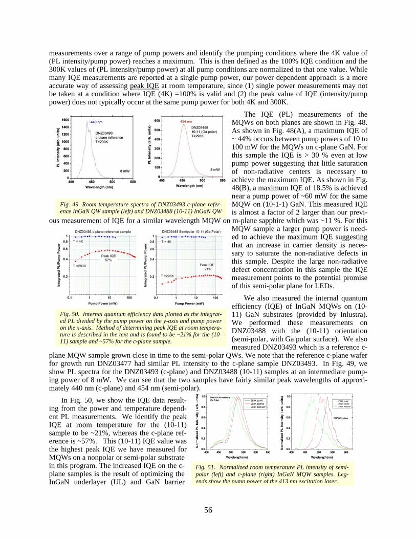
56
Fig. 49. Room temperature spectra of DNZ03493 c-plane refer-ence InGaN QW sample (left) and DNZ03488 (10-11) InGaN QW
Fig. 50. Internal quantum efficiency data plotted as the integrat-ed PL divided by the pump power on the y-axis and pump power on the x-axis. Method of determining peak IQE at room tempera-ture is described in the text and is found to be ~21% for the (10-11) sample and ~57% for the c-plane sample.
Fig. 51. Normalized room temperature PL intensity of semi-polar (left) and c-plane (right) InGaN MQW samples. Leg-ends show the pump power of the 413 nm excitation laser.
400 450 500 550 6000.0
0.2
0.4
0.6
0.8
1.0
Nor
mal
ized
PL
Inte
nsity
( ar
b. u
nits
)
Wavelength (nm)
293K 1mW 293K 10mW 293K 100mW
DNZ3521 cplane
400 450 500 550 600 6500.0
0.2
0.4
0.6
0.8
1.0 DNZ3503-84 semipolar(Ga Polar)
Nor
mal
ized
PL
Inte
nsity
( ar
b. u
nits
)
Wavelength (nm)
293K 1mW 293K 10mW 293K 100mW
measurements over a range of pump powers and identify the pumping conditions where the 4K value of (PL intensity/pump power) reaches a maximum. This is then defined as the 100% IQE condition and the 300K values of (PL intensity/pump power) at all pump conditions are normalized to that one value. While many IQE measurements are reported at a single pump power, our power dependent approach is a more accurate way of assessing peak IQE at room temperature, since (1) single power measurements may not be taken at a condition where IQE (4K) =100% is valid and (2) the peak value of IQE (intensity/pump power) does not typically occur at the same pump power for both 4K and 300K.
The IQE (PL) measurements of the MQWs on both planes are shown in Fig. 48. As shown in Fig. 48(A), a maximum IQE of ~ 44% occurs between pump powers of 10 to 100 mW for the MQWs on c-plane GaN. For this sample the IQE is > 30 % even at low pump power suggesting that little saturation of non-radiative centers is necessary to achieve the maximum IQE. As shown in Fig. 48(B), a maximum IQE of 18.5% is achieved near a pump power of ~60 mW for the same MQW on (10-1-1) GaN. This measured IQE is almost a factor of 2 larger than our previ-
ous measurement of IQE for a similar wavelength MQW on m-plane sapphire which was ~11 %. For this MQW sample a larger pump power is need-ed to achieve the maximum IQE suggesting that an increase in carrier density is neces-sary to saturate the non-radiative defects in this sample. Despite the large non-radiative defect concentration in this sample the IQE measurement points to the potential promise of this semi-polar plane for LEDs.
We also measured the internal quantum efficiency (IQE) of InGaN MQWs on (10-11) GaN substrates (provided by Inlustra). We performed these measurements on DNZ03488 with the (10-11) orientation (semi-polar, with Ga polar surface). We also measured DNZ03493 which is a reference c-
plane MQW sample grown close in time to the semi-polar QWs. We note that the reference c-plane wafer for growth run DNZ03477 had similar PL intensity to the c-plane sample DNZ03493. In Fig. 49, we show PL spectra for the DNZ03493 (c-plane) and DNZ03488 (10-11) samples at an intermediate pump-ing power of 8 mW. We can see that the two samples have fairly similar peak wavelengths of approxi-mately 440 nm (c-plane) and 454 nm (semi-polar).
In Fig. 50, we show the IQE data result-ing from the power and temperature depend-ent PL measurements. We identify the peak IQE at room temperature for the (10-11) sample to be ~21%, whereas the c-plane ref-erence is ~57%. This (10-11) IQE value was the highest peak IQE we have measured for MQWs on a nonpolar or semi-polar substrate in this program. The increased IQE on the c-plane samples is the result of optimizing the InGaN underlayer (UL) and GaN barrier
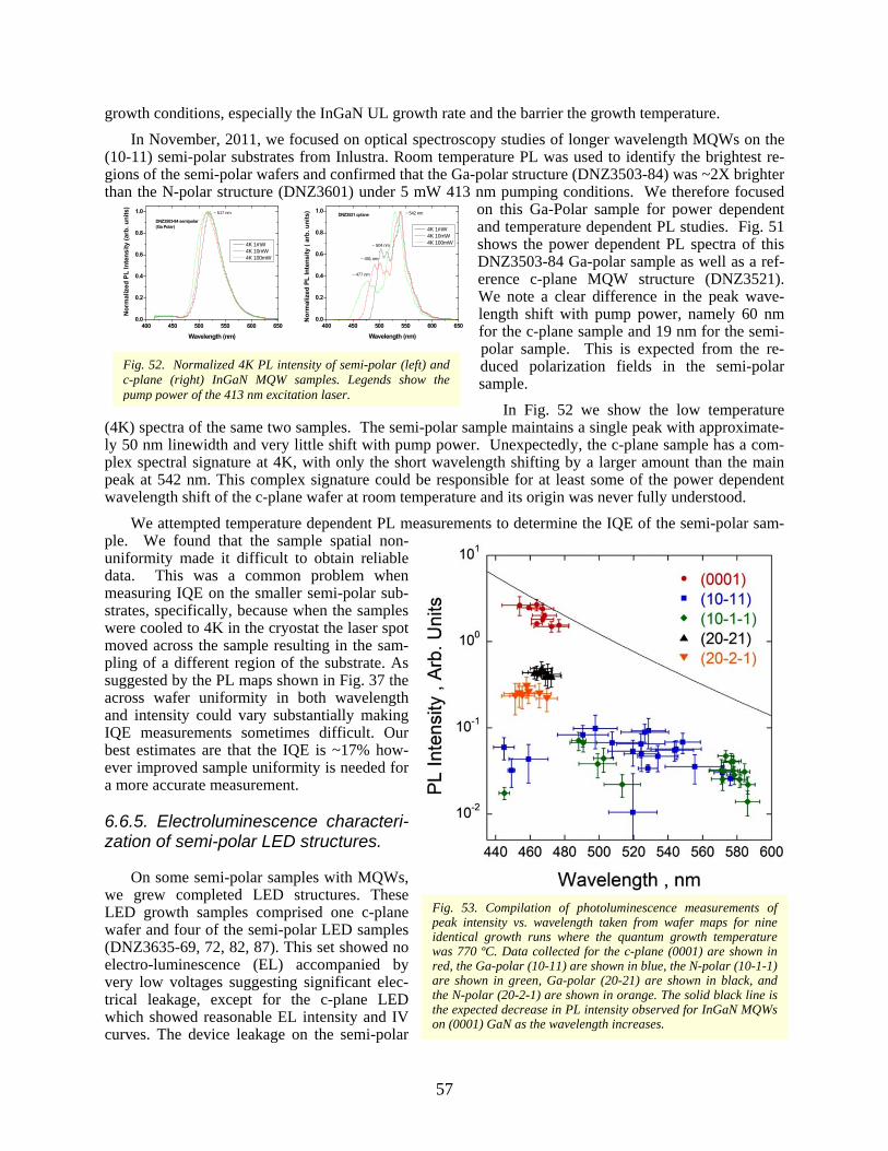
57
Fig. 53. Compilation of photoluminescence measurements of peak intensity vs. wavelength taken from wafer maps for nine identical growth runs where the quantum growth temperature was 770 ºC. Data collected for the c-plane (0001) are shown in red, the Ga-polar (10-11) are shown in blue, the N-polar (10-1-1) are shown in green, Ga-polar (20-21) are shown in black, and the N-polar (20-2-1) are shown in orange. The solid black line is the expected decrease in PL intensity observed for InGaN MQWs on (0001) GaN as the wavelength increases.
Fig. 52. Normalized 4K PL intensity of semi-polar (left) and c-plane (right) InGaN MQW samples. Legends show the pump power of the 413 nm excitation laser.
400 450 500 550 600 6500.0
0.2
0.4
0.6
0.8
1.0DNZ3503-84 semipolar(Ga Polar)
Nor
mal
ized
PL
Inte
nsity
(arb
. uni
ts)
Wavelength (nm)
4K 1mW 4K 10mW 4K 100mW
~ 517 nm
400 450 500 550 600 6500.0
0.2
0.4
0.6
0.8
1.0
~ 477 nm
~ 491 nm
~ 504 nm
~ 542 nmDNZ3521 cplane
Nor
mal
ized
PL
Inte
nsity
( ar
b. u
nits
)
Wavelength (nm)
4K 1mW 4K 10mW 4K 100mW
growth conditions, especially the InGaN UL growth rate and the barrier the growth temperature.
In November, 2011, we focused on optical spectroscopy studies of longer wavelength MQWs on the (10-11) semi-polar substrates from Inlustra. Room temperature PL was used to identify the brightest re-gions of the semi-polar wafers and confirmed that the Ga-polar structure (DNZ3503-84) was ~2X brighter than the N-polar structure (DNZ3601) under 5 mW 413 nm pumping conditions. We therefore focused
on this Ga-Polar sample for power dependent and temperature dependent PL studies. Fig. 51 shows the power dependent PL spectra of this DNZ3503-84 Ga-polar sample as well as a ref-erence c-plane MQW structure (DNZ3521). We note a clear difference in the peak wave-length shift with pump power, namely 60 nm for the c-plane sample and 19 nm for the semi-polar sample. This is expected from the re-duced polarization fields in the semi-polar sample.
In Fig. 52 we show the low temperature (4K) spectra of the same two samples. The semi-polar sample maintains a single peak with approximate-ly 50 nm linewidth and very little shift with pump power. Unexpectedly, the c-plane sample has a com-plex spectral signature at 4K, with only the short wavelength shifting by a larger amount than the main peak at 542 nm. This complex signature could be responsible for at least some of the power dependent wavelength shift of the c-plane wafer at room temperature and its origin was never fully understood.
We attempted temperature dependent PL measurements to determine the IQE of the semi-polar sam-ple. We found that the sample spatial non-uniformity made it difficult to obtain reliable data. This was a common problem when measuring IQE on the smaller semi-polar sub-strates, specifically, because when the samples were cooled to 4K in the cryostat the laser spot moved across the sample resulting in the sam-pling of a different region of the substrate. As suggested by the PL maps shown in Fig. 37 the across wafer uniformity in both wavelength and intensity could vary substantially making IQE measurements sometimes difficult. Our best estimates are that the IQE is ~17% how-ever improved sample uniformity is needed for a more accurate measurement.
6.6.5. Electroluminescence characteri-zation of semi-polar LED structures.
On some semi-polar samples with MQWs, we grew completed LED structures. These LED growth samples comprised one c-plane wafer and four of the semi-polar LED samples (DNZ3635-69, 72, 82, 87). This set showed no electro-luminescence (EL) accompanied by very low voltages suggesting significant elec-trical leakage, except for the c-plane LED which showed reasonable EL intensity and IV curves. The device leakage on the semi-polar

58
Fig. 54. Similar plot to the one shown in Fig. 1, except for a lower quantum well growth temperature of 740 ºC (shown within the blue circle). The red data points shown outside the red circle are for the c-plane (0001) identical growth runs where the QW growth tempera-ture was 770 ºC.
LEDs appears to correlate with cracks in the semi-polar substrates. Later in the program thick undoped GaN was grown by MOCVD in attempt to mitigate these leakage pathways within the bulk GaN sub-strates, resulting in an LED that is described in section 6.11.1.
6.6.6 MQWs on (20-21) semi-polar substrates.
The (20-21) semi-polar substrates were the third set of orientations chosen for this project. The Ga-polar and N-polar (20-21) substrates are in the same family as the previously studied orientation (10-11). Similar to studies reported in October, 2011, we re-peated our best blue MQW structure (optimized for (0001) GaN templates) on 7 of the Ga-polar (20-21) and 7 of the N-polar (20-2-1) substrates in 2 growth runs. The average PL intensity for these growth runs is plotted vs. the average wavelength from PL maps on the wafers in Fig. 53. In Fig. 53, the results for the Ga-polar (20-21) are shown as the black triangles while the results for the N-polar (20-2-1) are shown as the orange upside-down triangles. Also shown in Fig. 53 are the PL intensities for identical growth runs previously reported for growth on the (10-11) and (10-1-1) substrates. As shown in Fig. 53 the PL wave-length for both polarities of the (10-21) substrates are tightly grouped between 450 and 470 nm, similar to the results on (0001). In general, the PL intensities are ~2x larger on the Ga-polar (20-21) substrates com-pared to the N-polar (20-2-1) substrates. However both substrates have MQWs that have intensities ~10x less than MQWs on (0001).
We also conducted one growth run where the MQW growth temperature was lowered to 740 ºC to de-termine if more indium could be incorporated into the MQW to increase the emission wavelength. These results are shown in Fig. 54 (within the blue circle). As shown in Fig. 54, the PL wavelength increases as expected on both semi-polar substrates, however the shift is not as large as the wavelength shift measured on (0001) nor do they produce PL intensities higher than on (0001). We therefore concluded that the (20-21) semi-polar orientation is not likely a favorable orientation for producing brighter green or higher wavelength emitting LEDs.
6.7. Subtask 2.3: Determine the semi-polar orientati on that provides the highest IQE at 540 nm.
Again our major focus in the second year was to determine which semi-polar orientation has the abil-ity to achieve the longest wavelength MQWs while simultaneously producing good emission intensity. Once the longer wavelength substrate was chosen, we then intended on optimizing the IQE for 540 nm emission.
From the work in Section 4.6, it was obvious that the most promising substrate was the Ga-polar (10-11) and N-polar (10-1-1) orientations. We were able to achieve in the 2nd year an IQE around 17 % for 530 nm MQW on (10-11), suggesting that this orientation was the most promising. Unfortunately, only regions on the samples appears to produce this level of PL intensity and improvements in crystal quality were obviously necessary to meet the program goal of producing a 530 nm green LED with an IQE of 50%. Also improvements in the crystal quality of the substrates would have allowed MQW and LED

59
Fig. 55. Representative PL scans of Mg doped GaN films with c-plane, m-plane and (10-13) orientations.
evaluation by x-ray diffraction which we believe is necessary for obtaining a complete understanding of the grown structures.
6.8. Subtask 2.4: Develop p-ty pe doping on m-plane and semi-polar orientations for LEDs.
In the third year of this program we intended on developing LEDs to measure the EQE of our bright-est InGaN MQWs. To enable this possibility we spent part of the 1st year and the end of the second year developing p-type doping on nonpolar and semi-polar substrates. We intended on using PL and Hall Ef-fect measurements to determine the hole con-centrations on top of a undoped GaN layer, however electrical shorting issues, which also complicated the development of LEDs, also limited our ability to conduct Hall Effect measurements. Instead we qualitatively as-sessed the p-type doping of the various non-polar and semi-polar substrates. In this sec-tion we highlight our work on Mg doping of c-plane, m-plane, and (10-13) semi-polar GaN substrates.
For our initial study of Mg doping, we used our standard growth condition for Mg doped GaN on c-plane sapphire. For the p-type doping we used bis-methylcyclopendadienyl-magnesium (Mecp2Mg) as the metalorganic precursor. Typically, c-plane p-GaN films are grown at 200 torr at 970 ºC at a growth rate of ~0.6 µm/hr. using a Mecp2Mg flow rate of 30 sccm (which corresponds to 0.16 µmoles/min of the Mg precursor). Using these growth conditions ~3x1019 cm-3 Mg atoms are incorporated into the lattice resulting in routine hole concentrations of 3-5x1017 cm-3, after standard conditioning runs are conducted.
Using these standard p-type growth conditions, the Mg doping flow rate was varied from 30 to 200 sccm and Mg doped films were grown for 2 hours on insulating c-plane GaN grown on sapphire and Inlustra supplied m-plane and (10-13) semi-polar substrates. Prior to the growth of the Mg-doped GaN an undoped GaN was grown on all three co-loaded substrates in the hope of electrically isolating the p-type GaN from the underlying n-type substrate. The Mg doped GaN films were activated in the MOCVD reac-tor after growth by annealing in flowing N2 at 830 ºC for 10 min. prior to cool down.
Representative PL scans of the Mg doped GaN are shown in Fig. 55. These scans were chosen specif-ically to highlight the common PL signatures observed when c-plane GaN is doped p-type using Mg, which also appear on both the m-plane and (10-13) semi-polar planes. As listed in Fig. 55, the PL scans are for c-plane GaN doped using a 100 sccm flow rate, m-plane GaN doped using 50 sccm flow rate, and (10-13) semi-polar GaN doped using 150 sccm. Note that the flow rate for each of the three PL scans is listed along with the GaN orientation in the upper right-hand legend.
The three common PL features observed when GaN is doped with Mg are the band edge emission peak at 364 nm, a broader donor-acceptor pair (DAP) band peak around 380-390 nm, and an even broader blue band emission peak around 440 nm. The origin of the blue band emission at 440 nm is not entirely clear, however, it has been attributed to possible Mg defect levels or Mg clustering which results when too much Mg is incorporated into the GaN film.

60
Fig. 56. Plots of PL intensity for the DAP band in red and the blue-band in blue vs. Mg flow rate Mg doping of c-plane, m-plane, and (10-13) sub-strates.
Fig. 57. Hall Effect data for p-type GaN grown on c-plane sapphire. The hole concentration and resistivity are plotted vs. the cp2Mg flow rate. The Hall Effect data were measured from 5 different locations from the wafer flat to the wafer top using annealed indium metal contacts.
The intensity of these three common PL features depends on the Mg doping level. At low Mg levels, the PL luminescence is dominated by band-edge emission at 364 nm as shown in the blue m-plane scan in Fig. 55. As the Mg flow increases the DAP band increases in intensity and the band-edge intensity decreases as shown by comparing the blue and green scans. Finally, as the Mg doping level increases further, the blue band luminescence increases in intensity along with a corre-sponding decrease in the DAP band as shown by com-paring the green and red scans. Despite slight wave-length shifts in the positions where the DAP and blue-bands occur, the trend in intensities of all three of the major PL signatures is observed on all three substrates as the Mecp2Mg flow rate increases. The major differ-ence is the flow rate of Mecp2Mg that is required to produce where the band-edge, DAP, and blue band transitions occur.
For p-type GaN grown on c-plane, we have found that the hole concentrations (as measured by Hall Effect measurements) can be correlated to the measured PL intensities of the DAP and blue-bands. We find optimal hole concentrations when the DAP band is decreasing in intensity and the blue-band is increasing in intensity. As a quantitative reference point we define the DAP/blue band crossover point when the PL peak emission intensity of DAP and blue bands are equal. This quantification is shown in Fig. 56 where the DAP (red) and blue (blue curve) band intensities are plotted as a function of the Mecp2Mg flow rates. Extrapolating between the 30 and 50 sccm flow rates suggests a DAP/blue band cross over near 44 sccm for Mg doped GaN on c-plane GaN templates. On the m-plane and (10-13) semi-polar substrates the DAP/blue band cross
over point occurs at higher values, 70 and 130 sccm, respectively. Note that these cross over points will be used primarily as guidance to determine what Mecp2Mg dopant flow rate might produce the highest hole concentrations in these films, and hopefully we will be able to verify these using Hall Effect measurements,
The reason a higher Mg flow rate is required to achieve the DAP to blue-band cross over is not en-tirely clear, however, it could be related to a possi-ble decrease in the Mg incorporation efficiency on the non- and semi-polar substrates. Another possi-bility is that more Mg is necessary to compensate residual n-type defects in the non- and semi-polar

61
substrates. A third possibility is that the onset of Mg clustering or inversion domains do not occur as read-ily on the non- and semi-polar surface compared to the c-plane as pointed out by McLaurin et al. [46].
Attempts to measure the hole concentrations from the series of Mg doped samples were attempted us-ing Hall effect measurements. For some of the samples on the semi-polar substrates holes concentrations of ~1x1018 cm-3 were measured, however, the symmetry of the measured voltages and other reliability factors limit the confidence for these measurements making them somewhat questionable. The unreliabil-ity of the Hall measurements and electrical shorting were major impediments to measuring hole concen-trations on the semi-polar substrates, resulting in us using exclusively PL measurements to access ideal Mg flow rates.
Later in February of 2012, we revisited p-type doping of the Ga- and N-polar substrate orientations which we have recently been depositing InGaN MQWs. Before investigating p-type doping the semi-polar GaN substrates, we revisited baseline p-type doping of c-plane GaN using dopant flow rates rang-ing from 15 to 90 sccm. The hole concentrations and resistivities were averaged over 5 regions along the length of the wafer from the wafer flat to the wafer top as shown in Fig. 57. A peak hole concentration of 1.6x1018 cm-3 occurred at a cp2Mg flow rate of 30 sccm and decreased at lower and higher cp2Mg flow rates. This hole concentration is ~3 times higher than previous measurements of hole concentration in our
MOCVD reactor and we are still trying to understand what caused this increase. One possible explanation was that during the MOCVD reactor clean we replaced the inlet screen which delivers the metalorganics into the growth chamber. This is only speculative, however, since this possibility is hard to test since the exact nature of how the screen would influence hole concentrations is difficult to discern. Another change that we observed is that a 30 sccm flow rate of cp2Mg now provides the best hole concentration, while before the previous reactor clean ~44 sccm flow rates cp2Mg provided optimal hole concentrations as re-ported in the November 2010 monthly progress report.
Since, we previously described how optimal hole concentrations can be correlated to the measured PL intensities of the DAP and blue-bands. We found optimal hole concentrations when the DAP band de-creases in intensity and the blue-band increases in intensity. For the growth experiments performed this month we qualitatively estimated this cross-over point. Based on this estimation of the cross-over point we have listed in Table 2 the optimal cp2Mg flow rates for all of the polar (0001), nonpolar (1-100), and semi-polar planes that we have studied to date. For the first three substrate orientations shown in the table, the cp2Mg flow rates shown in parentheses () were measured using the older doping conditions which required higher doping flow rates. The values shown in Table 2 for these first three substrates were recal-culated based on the current optimal flow for c-plane GaN of 30 sccm and in the older optimal flow of 44 sccm. From these studies, we will use cp2Mg flow rates of 40 sccm for the LEDs we intend to grow on the (10-11) and (10-1-1) semi-polar substrates.
6.9. Subtask 3.1: For best semi-polar plane, develop miscut wafers and deliver to Sandia.
To reach this goal, we will pick the semi-polar orientation with the highest IQE and develop miscut wafers to further optimize the IQE. Similar to the first and second year we will determine the maximum indium concentration obtainable and then optimize emission at 540 nm with high IQE. Once we chose to use the (10-11) semi-polar orientation, miscut angles around both the (10-11) and (10-1-1) substrates were investigated.
Table 2: Estimated best cp2Mg flow rates from PL measurements to obtain optimal doping levels.

62
Fig. 58. Photoluminescence of polar and semi-polar InGaN QWs plotted as a function of the QW growth time. For each sample the PL wavelength (red circles) is plotted along the left axis and the PL intensity (blue squares) is plotted along the right axis. Note that the right axis has loga-rithmic units.
Unfortunately in the third year of this work, our partner in the program, Inlustra went out of business. Prior to shutting down, many (10-11), (10-1-1), (20-21), and (20-2-1) substrates had been delivered to-ward the end of the second year. Although, these substrates were of similar quality to the previously de-livered samples, they allowed us to eventually construct a working LED on a (10-11) semi-polar substrate as shown in Section 4.11. We also were able to obtain substrates from Kyma and Ammono which helped us finish the program. However, since our experience with this set of bulk GaN wafers was more limited due to fewer samples, we were able to build a working LED on a (20-21) semi-polar substrate from Am-mono. In addition, the x-ray diffraction from the MQWs and LEDs grown on the Ammono substrates produced strong intensity InGaN/GaN MQW features which indicated an improvement in the crystalline quality of these GaN substrates.
6.10. Subtask 3. 2: Determine ma ximum indium in MQW on miscut semi-polar GaN substrates.
We had previously looked varying the miscut and QW growth rate in conjunction with QW growth temperature. This work is described in Section 4.6.2 and occurred in the 2nd year of the program. One of the last optimizations we tried was to vary the InGaN QW thickness on both the (10-11), (10-1-1), (20-21), and (20-2-1) semi-polar orientations. For this study we used our standard blue multiple quantum well (MQW) recipe which consists of an InGaN QW grown for ~2.0 min (2.7 nm) with an indium concentration of ~15% at a temperature of 760 ºC. The 5 period MQWs are grown on a 4% indium InGaN underlayer that has a thickness of 180 nm. In previ-ous samples we have observed that these growth conditions produce c-plane MQWs emitting at 440 nm with IQEs of ~70%.
Because of the strong polariza-tion fields along the c-axis direction, the wavefunction overlap and result-ing emission intensity dramatically decreases as the c-plane QW thick-ness increases. The influence of the QW thickness on the PL intensity is shown in the top graph in Fig. 58. The PL intensity for QWs on the (0001) substrate decreases by over a factor of 100 as the QW thickness growth time increases from 2.2 to 4.8 minutes. Also note that the peak PL wavelength increases as the QW thickness increases from 440 nm to 475 nm. Both of these characteristics of the PL emission intensity and wavelength shift are due to the decreased overlap of the electron and hole wavefunctions caused by the strong polarization fields along the c-axis direction.

63
Fig. 59. X-ray diffraction ω/2θ scan of the as grown MQW (red line) on c-plane GaN on sapphire and the subsequent p-side layer grown to complete the LED structure.
For InGaN MQWs on the semi-polar substrates the influence of the polarization fields is reduced and thicker QWs can be used while maintaining good wavefunction overlap. Another added benefit of the thicker QWs is the carrier density can be spread over a larger volume, resulting in a reduced influence of Auger type non-radiative recombination that occurs at higher current densities. As shown in the lower four images in Fig. 58, the decrease in the PL intensity is substantially reduced for the semi-polar sub-strates compared to that on (0001). For the (10-11) substrates, the PL intensity decreases by a factor of 2 and the wavelength is maintained close to 500 nm. For the (10-1-1) substrates, a longer wavelength is maintained near 550 nm and the PL intensity is fairly constant for the QW growth time of 2.2 to 3.5 min. Similar trends are observed for the (20-21) and (20-2-1) substrates. This study demonstrates that QW thicknesses approaching 6 nm (3.5 min in this study) can used for LED structures without the loss of PL or EL intensity. These thicker QW might allow these semi-polar LEDs to be run at higher current densi-ties without the strong efficiency droop which is observed on c-plane LEDs at high drive current. Once we had completed this study our next major goal work to produce a working electro-luminescent device, which on the Inlustra substrates required the growth of thick undoped GaN prior to the LED growth.
6.11. Subtask 3. 3: Develop LED on optimal miscut semi-polar GaN substrate, determine EQE.
LED structures were developed based on single or multiple QWs grown on the various semi-polar substrates. On top of the QWs, a p-type AlGaN electron block layer was grown followed by a p-GaN con-tact layer. For rapid turnaround, “quick-test” LEDs using In-metal contacts were used, and on-wafer test-ing will be performed to get an early indication of the performance of the LED wafer. It was our hope that by using this rapid “quick-test” method we would be able to quickly optimize the p-side of LEDs.
For the first set of growth runs we used (10-11) and (20-21) semi-polar orientations (both Ga- and N-polar) along with MQWs grown on c-plane GaN on sapphire. Next the same p-side AlGaN electron block and p-GaN as we use for a c-plane LED structure was grown. The complete procedure for p-side consisted of heating the wafers up to the growth temperature of the last QW (~760 ºC) growing a thin GaN barrier layer followed by continued heating to 930 ºC for a ~25 nm thick AlGaN electron block layer and ~150 nm thick GaN layer. The difference in x-ray diffrac-tion between the as grown MQW structure and the completed LED structure is shown in Fig. 59 for growth on c-plane GaN on sapphire. Both the AlGaN electron block and GaN layer are visible in the XRD diffraction scan as peaks near ω ~ 17.5º.
These LEDs structures were “quick-tested” by applying indium contacts to the front p-GaN surface and scratching down to the n-GaN region to contact with indium. For the LED on c-plane (0001), the “quick-test” produced an average light intensity output compared to other standard LEDs on c-plane using this same growth recipe. However the LEDs on the Ga-polar (10-11) and N-polar (10-1-1) semi-polar substrates had electrical shorts preventing any measureable light output. The semi-polar LEDs were also electrically shorted when the n-side contact was moved to the back of the semi-polar substrate, suggesting that both lateral (top surface contact) and verti-cal (from bottom to top of the LED) testing produces shorting. It is believed that the shorting is caused by macroscopic defects or cracks within the bulk semi-polar substrates which are electrically conductive; however the exact nature of the electrical shorting was never clearly identified.

64
Fig. 61. Similar time progression as shown in Fig. 60 These images were taken from a smooth region of the substrate. The magnification is 10x.
Fig. 62. Nomarski images of semi-polar (10-11) surface morphology a) prior to growth, and b) after the growth of 10 microns over a region that contains a macroscopic crack. The magnification is 10x.
Fig. 60. Nomarski images of semi-polar (10-11) surface morphology a) prior to growth, b) after the growth of 10 microns, and c) after the growth of 20 microns. These images were taken from the same region near the corner of the semi-polar piece. The magnification is 10x.
6.11.1. LED development on thick undoped GaN layers.
In an effort circumvent the electrical shorting issues associated with LED growth on the semi-polar substrates, 20 microns of undoped GaN was grown on top of the semi-polar GaN substrates prior to the growth of the MQW and LED structures. The growth morphology progression of this thick GaN on the semi-polar substrates is shown in Fig. 60. In Fig. 60, Nomarski images of the as received substrates are shown near one of the substrate corners in Fig. 60(a) and images of the same corner after the growth of 10 and 20 microns are shown in Fig. 60(b) and 60(c). Several growth morphology changes are observed when GaN is grown including ran-dom crystallite growth near the bottom of the image, larger regions which appear to have smooth mor-phology around the edge of the substrate and a somewhat rougher looking region where possible step bunching is evident near the top of the images shown in Figs. 60(b) and 60(c). The evolution of the step bunched region is also seen in the images in Fig. 61 over a region where the substrate is initially rela-tively smooth. In Fig. 62, images are shown of a crack in Fig. 62(a) and the same region is shown in Fig. 62(b) after 10 microns of growth. We tried to locate the same region after 20 microns of growth but could not locate this same region suggesting that we may have overgrown this crack region. Our hope was that by coa-lescing GaN over the crack regions electrical shorting could be pre-vented when testing the LEDs in a lateral configuration.
After the growth of the 20 microns of undoped GaN an additional 5 microns of silicon doped GaN was grown on the substrates, followed by an InGaN underlayer and a 5 period multiple quantum well (MQW). The photoluminescence (PL) measurements of these MQWs are shown in Fig. 63 where the

65
Fig. 64. Electroluminescence spectrum of an LED on a (10-11) semi-polar substrate.
Fig. 63. Plot of the peak PL intensity vs. the PL wave-length for MQWs mapped over the entire c-plane (0001) wafer and the (10-11) and (10-1-1) semi-polar substrates. The MQWs were grown after the growth of 20 microns of undoped GaN and 5 microns of Si doped GaN. The average wavelengths and standard devia-tions for the various surface planes are 474 ± 8 nm for the (0001), 514 ± 16 nm for the (10-11), and 559 ± 11 nm for the (10-1-1).
peak PL intensity is plotted as a function of the peak PL wavelength for the c-plane (0001) template and the (10-11) and (10-1-1) semi-polar substrates. Even though the roughness of the semi-polar substrates increases after the growth of 25 microns of GaN, the MQWs maintain the wavelengths that we have pre-viously reported. For the various surfaces we meas-ured wavelengths of 474 ± 8 nm for the (0001), 514 ± 16 nm for the (10-11), and 559 ± 11 nm for the (10-1-1).
LED structures were completed on these MQW samples and then electrically tested and only one of the LEDs was found to not be electrically shorting. For the “quick-test” measurement, the samples were processed with In metal contacts for electrolumines-cence characterization. Most of the samples had very low light emission and evidence of electrical shorting. One sample, DNZ03980-047, performed significantly better than the rest. In Figure 64, we show the electroluminescence spectra, demonstrat-ing a main peak at 476 nm and a second peak at 409 nm, likely due to the InGaN underlayer beneath the MQW stack. While this sample showed the highest measureable electroluminescence (EL) to date, it is 10x less than the EL intensity measured for similar
wavelength LEDs on c-plane GaN on sapphire.
We also suspected that the lack electrical injec-tion might also be due to the lower hole concentra-tions. After about 2 dozen growth runs we have got-ten our hole concentrations back to > 5x1017 cm-3 for p-type GaN. We then grew additional thick GaN lay-ers on 11 different semi-polar pieces. The thickness of the deposited GaN is ~25 μm thick as measured by variable wavelength optical reflectance on a c-plane GaN on sapphire witness wafer. For these thicker GaN layers the growth pressure was varied from 500 torr to 100 torr for 6 cycles of 1 hour each. Our goal by varying the growth pressure was to in-troduce increased carbon in GaN (at lower pressure) to make the crystals more insulating. LEDs on these thick GaN substrates also showed significant electri-cal leakage making EL measurements to difficult and this approach for improving the electrical isolation from the Inlustra substrates was abandoned.
6.11.2. LED development on other vendor’s semi-polar substrates.
Since the Inlustra substrates had electrical shorting issues, we started using GaN substrates from two different sources which we will be evaluating for the remainder of this program. These substrates are a combination of non-polar and semi-polar orientations some of which we have previously studied. From Ammono we have obtained 2 m-plane and 3 (20-21) semi-polar substrates and 12 collaboration samples

66
Fig. 65. Plot of the normalized photoluminescence intensity vs. wavelength for a 5 period MQW structure grown simultaneously on 4 different surface orienta-tions of GaN. The blue circles are from GaN film grown on c-plane sapphire, while green circles repre-sent the bulk c-plane sample, red circles represent the bulk m-plane sample, black the bulk a-plane sample, and orange the (10-11) semi-polar sample. The solid line shows the usual decrease in PL intensity as the wavelength increases which has been observed for MQWs on c-plane heteroepitaxial GaN.
Fig. 66. Summary plot for previous (open symbols) and current results (filled symbols) showing the average peak photoluminescence intensity as a function of wavelength.
from Kyma, including two each; m-plane, a-plane, (11-22), (10-11), and one each; c-plane, (20-21), (10-13), and (10-12).
In Fig. 65 we show a comparison of the photo-luminescence intensity as a function of wavelength for MQWs placed on our heteroepitaxial GaN on sapphire substrates and four Kyma substrates with orientations along the c-plane (0001), m-plane (10-10), a-plane (11-20), and the (10-11) semi-polar plane. The QW growth temperature is 760 ºC which typically produces blue wavelength QWs (450 nm) on c-plane GaN on sapphire, but has been shown to produce wavelengths of 530 nm on (10-11) and 580 nm on (10-1-1). For Fig. 1, the peak PL intensity is plotted as a function of wave-length from the many data points measured across the entire PL map for each substrate. For the MQW on the heteroepitaxial GaN, the peak inten-sity occurs at wavelengths ranging from 440 to 450 nm as shown by the small blue circles. On the c-plane Kyma substrate, the peak wavelength is shifted to slightly shorter wavelengths ranging from 420 to 440 nm. The main reason for the dif-ference in peak wavelength between the two sub-strates may be the degree of contact with the wafer carrier during growth. Since the heteroepitaxial GaN is likely bowed during the MQW growth, contact with the wafer carrier is reduced resulting in lower actual growth temperature and higher indi-um concentration in the QWs. Conversely, the bulk GaN wafers are flat and likely make better
contact with the wafer carrier, resulting in a higher actual temperature and lower indium concentration in the QWs. The lower intensity on the Kyma c-plane wafer might be due the MQW structure not being op-timized for growth on this substrate. For the other crystal orientations, the MQWs on the a-plane GaN had the lowest wavelengths (~370 nm), followed by the m-plane (~ 410 nm), and the (10-11) semi-polar plane (~480 nm). The MQW on the m-plane appears to have a longer wavelength component near 440 nm; however, the PL intensity for this longer wavelength component was obtained from a smaller, more highly defective region on this crystal.
The results for these MQWs are compared to pre-vious growth experiments on c-plane and the (10-11) and (10-1-1) semi-polar substrates from Inlustra are shown in Fig. 66. As shown in Fig. 66, the c-plane and (10-11) wavelengths on the bulk crystals (filled sym-bols) are similar in range to the wavelengths expected for these two crystallographic orientations. In particu-lar, the PL wavelengths on the (10-11) semi-polar sub-strate is longer in wavelength than for the Kyma c-

67
Figure 67. Plot of the (a) photoluminescence (PL) wavelength and result-ing (b) indium fractions (indium concentrations) for InGaN underlayers grown on six different GaN crystallographic orientations. The x-axis is the angle from the c-plane either along the a-axis (for (11-2x) planes) of the m-axis (for (10-1x) and (20-21). The indium concentration was estimated assuming bulk emission and neglecting the influence of polarization fields.
Fig. 68. X-ray diffraction (XRD) scan (red) for 5 period multiple quantum well (MQW) on an InGaN underlayer on c-plane GaN grown on sapphire. The blue line is the dynamic diffraction anal-ysis of the XRD scan, yielding the fitting parameters a 3.3% indi-um concentration for the 197 nm thick InGaN underlayer and a MQW structure with 2.6 nm thick QWs containing 14.2% indium surrounded by 6.7 nm thick GaN barriers. The order of the su-perlattice peaks are denoted by the (…-2, -1, 0, +1…) labels with a measured superlattice spacing of 9.3 nm (QW + GaN barrier thicknesses).
plane substrate and other c-plane heteroepitaxial substrates and is in the correct range to produce green wavelengths LEDs.
To better understand the indium incorporation as a function of substrate orientation, a set of seven substrates were split into two groups along with a companion c-plane GaN on sapphire wafer. On these non-polar and semi-polar substrates we grew an InGaN underlayer (UL) at 850 ºC to a thickness of ~170 nm. On these InGaN films, photoluminescence and x-ray diffraction (XRD) measurements were made to
determine the indium concentration and estimate the thickness. Dynamic diffraction analysis of the InGaN films grown on the c-plane GaN wafers yielded indium concentra-tions of 3.3 and 3.5% and a thick-ness of ~170 nm. The measured PL wavelengths for the InGaN on the c-plane wafers were 376 and 377 nm. Following the correlation between bulk InGaN PL wavelength to indi-um concentrations developed by Wu et al. [14], we obtain indium con-centrations of 3.2 and 3.3 % which is close to the indium concentrations obtained from XRD.
Using the PL measurements from the non-polar and semi-polar substrates, we followed the same pro-cedure to estimate the indium concentrations on each of the substrates. As shown in Fig. 67(a), the meas-ured PL wavelengths are plotted vs. the inclination angle from the c-plane. (Note that following this defi-nition both m-plane (10-10) and a-plane (11-20) will have angles equal to 90º). In Fig. 67(b) the resulting indium concentration for each orientation following Wu et al. is esti-mated [14]. We found that the highest indi-um concentrations (~5.5 %) occur on the two (20-21) semi-polar substrates and the lowest concentrations (< 1%) occur on (10-12) and (11-20) substrates. This set of growth runs establishes that the (20-21) semi-polar substrate apparently incorporates more indium for this specific set of InGaN underlayer growth conditions and therefore the (20-21) substrates will be used to devel-op green wavelength LEDs.
On top of the InGaN UL, we grew mul-tiple quantum wells (MQWs) in two separate growth runs. The 5 period QWs were grown using our standard blue wavelength tempera-ture of 760 ºC and the GaN barriers at 800 ºC. Prior to the MQW growth, a 5 min. con-tinuation of the InGaN UL was first grown to prevent contamination or interface states near the MQWs. An XRD scan (red) for the MQWs grown on c-plane GaN is shown in Fig. 68 along with the dynamic diffraction analysis shown in blue. From the dynamic

68
Fig. 69. X-ray diffraction scans of the underlayer (UL) grown on the (20-21) substrate in blue followed by the multiple quantum wells (MQWs) on top of this growth in red. The order of the su-perlattice peaks are denoted by the (…-2, -1, 0, +1…) labels with a measured superlattice spacing of 9.4 ± 0.1 nm (QW + GaN barrier thicknesses).
Fig. 70. Demonstration of first blue-wavelength LED on (20-21) GaN substrate.
diffraction analysis we obtain the following fitting parameters; the InGaN UL has a 3.3% indium concentration and is ~200 nm thick; and the InGaN MQW structure has QWs that contain 14.2% indium and a thickness of 2.6 nm thick surrounded by 6.7 nm thick GaN barriers. In Fig. 68, the diffraction order of the superlattice peaks are denoted by the (…-2, -1, 0, +1…) labels and have a superlattice spac-ing of 9.3 nm (QW + GaN barrier thickness-es). For both c-plane GaN wafers the PL peak wavelengths were 433 ± 2 nm and 437 ± 2 nm as measured over the center inch diameter of the wafer. This is the same region that the non-polar and semi-polar reside in during growth in the 1/4 inch wafer cutouts.
In Fig. 69 we show XRD scans for the InGaN UL and MQW grown on an Ammono (20-21) bulk substrate. The ω/2θ radial scan for the substrate and the InGaN UL is shown in blue and is offset from the MQW scan by dividing the scan intensities by 10. The XRD signal was aligned on the InGaN UL peak, and as shown in Fig. 69, the substrate peak
occurs near 35.25º and the InGaN UL peak occurs near 34.9º. Based on the PL peak wavelength for this UL the estimated indium concentration is 5.6 ± 0.6 % which is 70% more indium than found on the c-plane GaN for the same growth conditions.
After the MQW growth, the XRD was again aligned to the InGaN UL peak resulting in the scan shown in red in Fig. 69. The key peak positions are labeled and include the GaN template, InGaN UL, and the MQW superlattice peaks denoted by the (…-2, -1, 0, +1…) labels. Measurement of the angular distance between the superlattice peaks give a spacing of 9.4 ± 0.1 nm (QW + GaN barrier thicknesses) which is very similar to the spacing of 9.3 nm for the superlattice spacing on c-plane GaN as mentioned above. For this wafer the PL peak wavelength near the center was 454 nm, which is longer than the 437 nm measured on the companion c-plane wafer, suggesting more indium incorporation (< 15%) on the (20-21) substrate compared to the (0001) wafer.
On top of the MQW grown on top of the (20-21) sub-strate from Ammono, we completed the LED structure. The LED’s p-side structure consisted of a p-type AlGaN elec-tron block layer followed by a p-type GaN epilayer, with the entire p-side grown at a temperature of 970 ºC. In elec-troluminescence (EL) quick-test studies, the LED exhibited a blue-emission wavelength at ~450 nm as shown in Fig. 70; this wavelength is similar to the wavelength previously measured in photoluminescence studies of the same sam-ple. The EL intensity was ~50-100 smaller than observed for similar-wavelength LEDs grown on c-plane sapphire. Considering that the (20-21)-oriented LED heterostructure was constructed from three different growth runs, with characterization performed in between each growth, we consider the observed EL a promising first result on these new substrates.

69
Fig. 71. x-ray diffraction (XRD) scans for a 5-period multi-ple quantum well (MQW) grown on a (20-21) GaN substrate. The red scan was measured with the substrate’s a-plane surface nor-mal oriented perpendicular to the diffraction plane, and the blue scan was measured with the a-plane surface normal oriented parallel to the diffraction plane. For both scans the XRD intensi-ty was optimized for the InGaN underlayer (UL) peak. The plot-ted intensities in blue are vertically offset to facilitate visual comparison of the satellite peaks.
Figure 72. XRD scan measured with the sample’s a-direction oriented perpendicular to the diffraction plane. The colored scans are rocking-curve scans performed at the maxima of selected diffraction peaks seen in the initial ome-ga/2theta scan. The similarly narrow rocking-curve peakwidths seen for the InGaN UL, the MQW satellites, and the GaN substrate indicates that little or no strain relaxation is seen by XRD with the sample in the “perpendicular” ori-entation.
Using (20-21) x-ray diffraction (XRD), we also analyzed the as-grown MQW hetero-structure in order to determine additional structural aspects of the InGaN underlayer (UL) and the InGaN QWs. Figure 71 shows resulting ω/2θ radial scans measured using a complementary pair of orthogonal sample ori-entations (details of the sample orientations are described and illustrated in Fig. 71). For both scans, the XRD intensity was optimized using the (20-21) InGaN UL peak instead of the main (20-21) GaN diffraction peak, be-cause the optimal ω/2θ offset did not coincide for these two epilayers’ diffraction peaks. The observed lack of coincident alignment is per-haps a first indication of strain relaxation due to misfit-dislocation formation within the sample. The XRD intensity was divided by a factor of 10 for the scan along the c-direction to offset it from the scan along the a-direction. Note that the peak diffraction positions occur at similar values of ω for both scans.
Subsequent XRD rocking-curve studies of this sample (shown in Figs. 72 and 73) are also consistent with the occurrence of signifi-cant strain relaxation within the sample. Fig-
ure 72 shows a replot (solid black line) of the ω/2θ scan of Fig. 71 that was taken in the perpendicular sample orientation. In addition, Fig. 72 superimposes plots of rocking-curve scans (colored lines) that were measured about each selected maxima seen in the ω/2θ scan. Figure 73 is analogous to Fig. 72 except that it shows data taken in the parallel sample orientation. When comparing Fig. 72 to Fig. 73, note in Fig. 72 that the rocking-curve peakwidths are in all cases quite narrow. Howev-er, in Fig. 73, the rocking-curve peakwidths are substantially broadened for the InGaN UL and the InGaN/GaN MQWs, but the rocking curve of the GaN substrate remains narrow, just as in Fig. 72. The selective broadening of the just the UL and MQW peakwidths indicates the onset of ani-sotropic strain relaxation. This relaxation occurs by misfit-dislocation glide along a preferred line direction, as expected for InGaN growth on semi-polar GaN [47].
Given the observed peakwidth trends, we can further infer that the observed strain relaxation initiates during growth of the initial thick InGaN underlayer and likely continues during MQW growth. Clearly, defect generation during the InGaN UL or QW growth should be avoided since these defects are likely to produce de-creased radiative efficiency, as is the case for the LED shown in Fig. 70. We concluded that our

70
Table 3. Rocking curve linewidths for various XRD peaks measured with the sample oriented both perpendicular (2nd column) and parallel (3rd col-umn) to the a-direction on the semi-polar sample. The 4th column contains the ratio of the parallel to perpendicular FWHM.
Figure 73. XRD scan measured with the sample’s a-direction oriented parallel to the diffraction plane. The col-ored scans are rocking-curve scans performed at the maxi-ma of selected diffraction peaks seen in the initial ome-ga/2theta scan. The rocking-curve peakwidths for the InGaN UL and the MQW satellites are much broader while the GaN rocking-curve peakwidth remains narrow. The in-crease in the peakwidth of the UL and MQWs indicates that a large degree of strain relaxation is seen by XRD with the sample in the “parallel” orientation. The contrasting re-sults seen in Figs. 72 and 73 indicate that strain-relaxing dislocations in the sample are preferentially oriented along a single line direction.
Fig. 74. Structure of the single quantum well LED grown on the bulk GaN (20-21) substrate.
next growth run would avoid the thick InGaN UL (likely with higher indium concentration) under the MQWs structure and to possibly grow only a single- QW LED on the remaining two (20-21) semi-polar substrates. The resulting thinner InGaN/GaN heterostructures will be less likely to strain relax and are thus expected to have higher efficiency.
The structure of the LED is shown in Fig. 74, and consists of a single, thick, InGaN QW grown on a dilute indium concentration InGaN under-layer (UL). The single QW was capped with an undoped GaN spacer layer, followed by an Al-GaN electron block layer and a p-type GaN layer capped with a p-type contact layer. For this sam-ple the InGaN QW was thicker (~10 nm) com-pared to QWs on c-plane GaN (~2-3 nm) to take advantage of the increased electron/hole wave-function overlap due to the reduced polarization fields on this semi-polar plane. Also, the entire structure was grown in a single growth run to avoid interfaces exposed to air as was done in previous LEDs on semi-polar GaN.
XRD radial (ω/2θ) scans of the LED struc-ture are shown in Figs. 75 and 76. The main dif-ference between the two scans shown in Figs. 75 and 76 is that the crystal is rotated by 90º in Fig.
76 with respect to its’ orientation in Fig. 75. The scan in Fig. 75 was measured with the x-ray beam paral-lel to the nominal a-plane direction. In the diffraction scan, the main GaN substrate peak is labeled along with the InGaN underlayer (UL), the GaN single QW layer, and the AlGaN electron block layer. These peak structures can be identified by approximating a dynamic diffraction analysis through the measured diffraction data. Also shown in Figs. 75 and 76 are superimposed the rocking-curve scans (color lines)
that were measured at the selected maxima seen in the ω/2θ scans. The FWHM of the peakwidths measured in Figs. 75 and 76 are listed in Table 3, along with the value of the FWHM measured in Fig. 76 divided by the FWHM measured in Fig. 75 (column 4). From Table 3, it appears that the FWHM for the InGaN UL and the AlGaN EB lay-ers are similar to the underlying GaN substrate, while the FWHM for the InGaN QW is twice that of the underlying GaN substrate. A simi-lar trend is also observed in Fig. 76 where the FWHM for the UL and EB layers are similar to the substrate peak along this scan direction.

71
Fig. 77. ω/2θ x-ray diffraction (XRD) scan measured for the c-plane GaN on sapphire. The red scan is the measured x-ray signal and the blue curve is a dynamic diffraction analy-sis. The fitting parameters are listed in Table 4 in column 2.
Fig. 75. ω/2θ XRD scan measured with the sample’s a-direction oriented perpendicular to the diffraction plane. The colored scans are rocking-curve scans performed at the maxima of selected diffraction peaks seen in the initial ome-ga/2theta scan. The similarly narrow rocking-curve peakwidths seen for the InGaN UL, the MQW satellites, and the GaN substrate indicates that little or no strain relaxation is seen by XRD with the sample in the “perpendicular” ori-entation.
Fig. 76. XRD scan measured with the sample’s a-direction oriented parallel to the diffraction plane. The colored scans are rocking-curve scans performed at the maxima of select-ed diffraction peaks seen in the initial omega/2theta scan. The rocking-curve peakwidths for the InGaN UL and the MQW satellites are only slightly broader compared to measurements measured along the a-direction as shown in Fig. 75 and listed in Table 3. The slight increase in the peakwidths of the InGaN UL, InGaN QW, and AlGaN EB indicates that for growth along this direction, there might be a small degree of strain relaxation with the sample in the “parallel” orientation.
Note that the ratio of the FWHM observed in Fig. 76 are approximately 3.2 to 3.6 times those measured in Fig. 75. This may suggest a very slight relaxation along this direction, however, compared to the LED sample shown in Figs. 71 to 73, the relaxation is near zero.
Unfortunately, the LED structure shown in Fig. 74 did not produce any measureable electro-luminescence due to electrical shorting of the LED. Following this issue with electrical shorting, we de-veloped a 5 MQW version of the same LED structure shown in Fig. 74 on an Ammono (20-21) semi-polar substrate. Again the “quick-tested” of this sample showed shorting and did not produce any measureable electroluminescence. The XRD analysis of this sample also suggests that no sig-nificant strain relaxation of the MQW was ob-served. Rocking curve measurements through the main GaN, InGaN/GaN superlattice and AlGaN electron block layer showed no major peak broadening also suggesting no significant strain relaxation during the sample growth. This was the last Ammono semi-polar substrate that we had available for study.
Shown in Figs. 77 and 78 are the ω/2θ radial scans for the LED structure on c-plane GaN on sapphire (Fig. 77) and on the Ammono (20-21) semi-polar substrates (Fig. 78). The XRD exper-imental scans are shown in red and the dynamic diffraction fits are shown by the blue curves. The dynamic diffraction parameters used for the fit in Fig. 78 are for the (0004) XRD reflection. These

72
Table 4. XRD fits for the (0002) diffraction peak for Fig. 77 from the (0001) surface along with the fit for the semi-polar (20-21) for Fig. 78 using the (0004) diffraction fit denoted with (*).
Fig. 78. ω/2θ XRD scan measured with the sample’s a-direction oriented parallel to the diffraction plane. The red scan is the measured x-ray signal and blue curve is a fit using dynamic diffraction analysis. For the fit the (0004) dynamic diffraction analysis crystal parameters were used since this reflection is close to the (20-21) semi-polar c-plane spacing (see the text for details). The fitting parame-ters are listed in Table 4 in column 3.
values were used for the fit since the 2θ angles are close for the (0004) and (20-21) reflections and only (0002), (0004), and (0006) dynamic dif-fraction fits can be made with the current soft-ware. For the (0004) reflection the 2θ GaN peak is 72.85º, while for the (20-21) the 2θ GaN peak is ~70.50º, which means that the thicknesses es-timated by this approach for the (20-21) might be slightly underestimated. The fits for both the (0002) and the (20-21) are listed in Table 4 and the fits suggest that similar indium concentration is obtained in both structures. The wavelength of the LED could not be verified using photolumi-nescence (PL) since the p-GaN contact layer was too thick for adequate penetration of the laser to excite the MQW structure on both samples.
After using the last of the Ammono wafers, we ordered 6 more substrates with the expected arrival time of 8 week. On these substrates we eventually grew additional LED structures to conclude the program. The end date of this pro-gram was scheduled to be January 15th 2013; however, we asked for and were granted a no cost extension until April 15th, 2013 to complete the LEDs on the recently ordered Ammono sub-strates.
The new Ammono substrates arrived in March of 2013. On these substrates we grew InGaN MQWs on top of a dilute indium InGaN underlayer, simultane-ously, and after characterization we would grow the p-side contact layer. Before the growth of the MQW structure, a several micron Si doped GaN layer was grown, resulting in roughening of the (10-11) and (20-21) substrates and some roughening around the edges on the (20-2-1) substrate. The resulting radial XRD scans are shown in Fig. 79 for the MQW films grown on a) (0001) c-plane GaN on sapphire as well as the semi-polar substrates, b) (10-11), c) (20-21), and d) (20-2-1). The XRD scans with the clearest diffraction features were obtained on the (0001) and (20-2-1) sub-strates and dynamic diffraction fits (red line through data) for both of these scans are shown in Table 5. Be-cause dynamic diffraction scan for the (20-2-1) reflec-
tion was not available, we used the (0004) which as mentioned previously in this report is close the (20-2-1) reflection. The close fit between the (20-2-1) diffraction scan and the dynamic diffraction fit indicated that minimal lattice relaxation occurred during the growth of the MQWs on this substrate.
From the fit parameters listed in Table 5 there is good agreement in thicknesses and indium concen-tration between the two films, except for the indium concentration and thickness of the QWs. For the MQWs grown on c-plane GaN the 2.3 nm thick QWs had an indium concentration of 17 % while on the semi-polar (20-2-1) substrate the 2.9 nm thick QWs had a higher indium concentration of 25%. This is the clearest evidence that we have obtained in this program that the indium concentration on the (20-2-1) can be increased above that on (0001) using the same growth conditions.

73
Fig.79. XRD radial scans of the a) (0002), b) (20-21), c) (10-11), and d) (20-2-1) reflections. In the figure the GaN template peak is shown along with the InGaN underlayer (UL) peak, and the super lattice peaks denoted numerically from -10 to +6. The fits shown in red on figures a) and d) are from the dynamic diffraction analysis using the (0002) for a) and (0004) for d) shifted in angle to match up the GaN substrates peaks.
Table 5. XRD fits for the (0002) diffraction peak for Fig. 79 from the (0001) surface along with the fit for the semi-polar (20-21) using the (0004) diffraction fit denoted with (*).
The PL scans for all four samples are shown in Fig. 80. For these scans a pulsed 266 nm laser was used which tends to provide a higher peak power than the 325 nm HeCd cw laser that we have usually used for this work. From the PL scans shown in Fig. 80, the main GaN peak is observed near 360-365 nm and varies slightly depending on the substrate. In addition on the (0001) and (20-2-1) substrates there is a main MQW peak near 450 nm and almost non-existent peaks for the (10-11) and (20-21) substrates. We
were not able to ascertain if the decreased PL emission intensity was due to the increased substrate roughness, since only one set of samples was available for this study.
Full LED structures were grown on the second set of received substrates. LED “quick-tests” on these substrates did not produce any visible light due to electrical shorting. Shorting and weak emission inten-sity was also observed on the c-plane GaN substrate, suggesting there were issues with the p-type layers. In anticipation of this experiment, we grew and tested an

74
Fig. 80. PL intensity scans vs. wavelength for the MQWs XRD scans shown in Fig. 79. Only MQWs grown on the (0001) and (20-2-1) substrates have appreciable intensity near 450 nm.
LED on c-plane GaN. From this LED we did observe electroluminescence from the LED; however it was only half as bright as some of our brightest “quick-test” LEDs. Unfortunate-ly, we were not able to conclude the program with further examples of working LEDs on the Ammono bulk substrates.
6.12. Subtask 3.4: Develop 540 nm InGaN MQW struc-tures with IQE of 50%.
Our goal in this subtask was to use a standard process for top-emitting devices employing a semi-transparent NiO p-contact. We would then take the processed LED struc-tures will be diced into die and mounted on standard TO-type headers for testing. LED testing would have included L-I-V measure-ments using both CW and pulsed-current in-put and would have employed a calibrated integrating sphere to obtain quantitative values of LED exter-nal quantum efficiency. LED internal quantum efficiency will then be estimated from knowledge of the extraction efficiency of the particular LED chip geometry. Since we developed no promising LEDs from the “quick-test” surveys we were unable to proceed with work on this subtask.

75
7. COMPARISON OF ACCOMPLISHMENTS TO PROPOSED GOALS
The program milestones are listed in Table 6. The milestones are a combination of date driven ac-complishments proposed at the beginning of the program that we thought were necessary to reach the program goals, including quantitative measures of IQE and EQE in 540 nm emitting MQWs and LEDs. As described in Section 4.2.8, the IQE will be measured using variable-temperature PL measurements, while the EQE measurements will be performed using a standard LED package where the extraction effi-ciency is understood. These EQE measurements will then be scaled to reflect EQE measurements that should occur in a state-of-the-art package where the light extraction efficiency is ~80% or better.
Table 6.
Task 1. Develop InGaN MQWs on basal or miscut m-plane GaN substrates Months*
1.1 Develop epi-ready m-plane polished crystals at Inlustra and deliver to Sandia. 2
1.2 Determine maximum indium composition in MQWs on m-plane GaN substrates. 5
1.3 Explore MQWs on miscut m-plane GaN to determine maximum IQE** and wavelength. 9
1.4 Initial growth of MQWs on semi-polar to determine maximum IQE and wavelength. 12
Criterion for success: To establish wavelength and IQE limits of QW growth on miscut m-plane. The target for success is 540 nm with 20% IQE.
12
Task 2. Develop InGaN MQWs on semi-polar GaN substrates (3 different orienta-tions)
Months*
2.1 Develop epi-ready semi-polar polished crystals at Inlustra and deliver to Sandia. 13
2.2 Determine maximum indium composition in MQWs on semi-polar GaN substrates. 16
2.3 Determine semi-polar orientation that provides the highest IQE at 540 nm. 20
2.4 Develop p-type doping on m-plane and semi-polar orientations for LEDs. 22
Criteria for success: Down-select to orientations that give the highest MQW IQE and longest wave-lengths. The target for success is 540 nm with 35% IQE.
24
Task 3. Optimize InGaN MQWs on miscut semi-polar GaN substrates. Months*
3.1 For best semi-polar plane, develop miscut wafers at Inlustra and deliver to Sandia. 25
3.2 Determine maximum indium in MQW on miscut semi-polar GaN substrates. 28
3.3 Develop LED on optimal InGaN MQWs on semi-polar GaN substrates, determine EQE.*** 30
3.4 Develop 540 nm InGaN MQW structures with IQE of 50%. 32
Criteria for success: To develop 540 nm LED with an EQE of 40%. The EQE of the LED will be measured in a standard package and the light extraction will be estimated based on the standard package’s design.
36
* months are listed from the start date of the program. ** IQE of InGaN MQWs will be determined by temperature-dependent photoluminescence *** EQE values will be determined by LED L-I measurements using a calibrated integrating sphere. We estimate EQE values of ~20% from Fig. 1 which would be at state-of-the-art for this wavelength. Based on a 80% extraction efficiency [18]using advanced packaging and thin-film flip-chip designs we estimate an IQE of 25% at 540 nm as shown in Fig 1. Our EQE milestones of 40% in year 3 would be double the current estimated state-of-the-art. Low-er-end packaging strategies with reduced extraction efficiency will be employed for the LED fabricated in this pro-posal and the resulting EQE will be scaled appropriately to that would be expected in a state-of-the-art package.

76
7.1. Evaluation of Progress on First Year Milestones The Milestones for the first year are listed below along with the criterion for success in the first column. In the 2nd and 3rd columns are listed the proposed time frame from the start of the program and the actual completion data for each Milestone. Below the chart is the progress during the program for each Milestone.
Table 7.
Task 1. Develop InGaN MQWs on basal or miscut m-plane GaN substrates Months Actual Months
1.1 Develop m-plane polished crystals at Inlustra and deliver to Sandia. 2 6
1.2 Determine maximum indium composition in MQWs on m-plane. 5 10
1.3 Determine maximum IQE and wavelength on miscut m-plane GaN. 9 NA
1.4 Initial work on semi-polar to determine maximum IQE and wavelength. 12 12
Criterion for success: To establish wavelength and IQE limits of QW growth on miscut m-plane. The target for success is 540 nm with 20% IQE. 12 12
Subtask 1.1 – The program started on January 15th, 2010 after some delay in confirming the monies had arrived at Sandia. A contract for the non-polar and semi-polar substrates was in place by March 26th, 2010 and the first m-plane substrates delivered on June 30th. Prior to that deliver five m-plane practice wafers were received April 15th, 2010. The first semi-polar (10-13) wafers received Sept. 29th, 2010.
Subtask 1.2 – The maximum indium composition resulted in wavelengths as large as 535 nm, however PL luminescence intensity for this sample was very low. Better PL intensity was achieved for MQW on m-plane that had wavelengths around 480 nm which was determined to be not long enough for this pro-gram. We estimated that the indium concentration in these MQWs grown on m-plane GaN ranged from 20 to 25 %.
Subtask 1.3 – We decided not to complete this milestone, since we did not achieve > 500 nm emission for MQWs grown on m-plane.
Subtask 1.4 – Initial MQW growth runs were conducted on (10-13) and (10-1-3) semi-polar substrates received from Inlustra in September 29th, 2010.
Criterion for Success – We achieved MQWs on m-plane GaN with an IQE of 11% at a wavelength of 466 nm. The measured IQE was slightly over half of the target IQE and well short of the target wavelength of 540 nm.

77
7.2. Evaluation of Progress on Second Year Milestones The Milestones for the second year are listed below along with the criterion for success in the first column. In the 2nd and 3rd columns are listed the proposed time frame from the start of the program and the actual completion data for each Milestone.
Table 8.
Task 2. Develop InGaN MQWs on semi-polar GaN substrates (3 different orientations)
Months Actual Months
2.1 Develop epi-ready semi-polar polished crystals and deliver to Sandia. 13 13
2.2 Determine maximum indium composition in MQWs on semi-polar GaN. 16 18 - 24
2.3 Determine semi-polar plane that provides the highest IQE at 540 nm. 20 20
2.4 Develop p-type doping on m-plane and semi-polar orientations for LEDs.
22 12 (26)
Criteria for success: Down-select to orientations that give the highest MQW IQE and longest wavelengths. The target for success is 540 nm with 35% IQE.
24 24
Subtask 2.1 – The substrates we explored in the second year were the (10-13), (10-11), and (20-21). The-se substrates were regularly delivered regularly throughout 2nd year with the (20-21) substrates delivered in Nov. 2011. Both the Ga-polar (ex. 10-11) and N-polar (ex. 10-1-1) directions were developed for each of the substrates.
Subtask 2.2 – By August of 2011, we had determined that both the (10-11) and (10-1-1) produced MQWs with the longest wavelengths. However, we had not yet fully examine the (20-21) substrates until Decem-ber of 2011. Even after this evaluation of the (20-21) substrates the (10-11) and (10-1-1) still produced the longest wavelength MQWs of 530 nm on (10-11) and 580 nm of (10-1-1). The maximum indium incorpo-rated on these two semi-polar planes could not be determined from XRD.
Subtask 2.3 – The (10-11) and (10-1-1) semi-polar planes allowed us to get the longest wavelengths with the highest IQE.
Subtask 2.4 – The incorporation of Mg into the non-polar and semi-polar GaN planes was investigated in two separate timeframes, in December of 2010 and February of 2012. Due to electrical shorting and carri-er leakage Hall Effect measurements could not be routinely done and we had to rely on PL signatures to determine the ideal Mg doping flow.
Criteria for Success – We chose to use the (10-11) and (10-1-1) semi-polar planes for since these semi-polar planes produce the longest wavelengths. On (10-11) achieved IQE of 21% at a wavelength of 454 nm and 17% at a wavelength of 530 nm, and on (10-1-1) achieved an IQE of 18.5% at a wavelength of 473 nm. The (10-11) semi-polar plane at 530 nm was close in wavelength to our target wavelength and about on half the measured target IQE.

78
7.3. Evaluation of Progress on Third Year Milestones The Milestones for the third year are listed below along with the criterion for success in the first column. In the 2nd and 3rd columns are listed the proposed time frame from the start of the program and the actual completion data for each Milestone.
Table 9.
Task 3. Optimize InGaN MQWs on miscut semi-polar GaN substrates. Months Actual Months
3.1 For best semi-polar plane, develop miscut wafers and deliver to Sandia. 25 22
3.2 Determine maximum QW indium on miscut semi-polar GaN substrates. 28 22
3.3 Develop LED on best semi-polar GaN substrates, determine EQE.*** 30 39
3.4 Develop 540 nm InGaN MQW structures with IQE of 50%. 32 -
Criteria for success: To develop 540 nm LED with an EQE of 40%. The EQE of the LED will be measured in a standard package and the light extrac-tion will be estimated based on the standard package’s design.
36 40
Subtask 3.1 – Miscut semi-polar substrates of (10-11) and (10-1-1) were delivered toward the second year. The miscut directions were measured along the a- and c-directions; however the measured PL wave-length and intensity varied substantially across the substrates, making any definitive conclusions on the exact miscut needed to maximum indium incorporation impossible.
Subtask 3.2 – Since XRD MQW signals were weaker due to crystal mosaic, stacking faults, and lack of dynamic diffraction software, clear assessment of the indium concentration did not occur until MQWs were grown on Ammono (20-21) substrates
Subtask 3.3 – Many attempts were made to grow and test LEDs on Inlustra substrates, with the result of only one working adequately for a “quick-test”. Later we were also able to achieve one working LED on an Ammono substrate, however the EL intensity was too low to warrant further packaging for the deter-mination of EQE.
Subtask 3.4 – Not achieved due to LEDs having not enough EL intensity in the “quick-tests” and having too much electrical leakage.
Criteria for Success – We were able to achieved MQWs on (10-11) having had an IQE of 17% at a wave-length of 530 nm, but unfortunately not able to produce a LED with sufficient EL emission intensity to warrant packaging and further testing. We were close to our target wavelength of 540 nm (we achieved 530 nm) at about 1/3 of the target IQE of 50% (we achieved 17%).

79
Table 10. Summary of standard wavelengths, maximum wavelengths, and IQEs @ wavelengths that were achieved during this program. The first column gives the Miller indices of the substrates used. The second column lists the wavelength achieved using our standard blue MQW recipe on c-plane GaN. The * denotes substrates that were provided by Kyma Tech-nologies Inc. The third column lists the maximum wavelength of MQW achieved on each substrate. The fourth column lists the IQE at wavelength for the variable temperature PL measurements were made. The ** is because independent of the cur-rent program we have achieved IQE > 90 % on c-plane GaN as reported by Guan-Bo Lin and coworkers [5]. The § symbol denotes that the piece used for this measurement moved in the cryostat so that the IQE could only be estimated. The last col-umn denotes the substrates on which a working LEDs were obtained.
8. CONCLUSIONS
We summarize our work on this project in Tables 6 and 7. In Table 6 is listed the various polar, non-polar, and semi-polar substrates studied in the program along with the resulting wavelength, IQE, and LED information. Our goal here is to determine which orientations of GaN incorporate the most indium for a given growth temperature so that the substrates can be ranked to determine the most promising can-didates for future work.
One of our standard tests was to determine the MQW wavelength for a standard 440 nm MQW recipe that we have developed for c-plane GaN. The wavelength results for each of the substrates are listed in the second column in Table 6. From this evaluation both the non-polar substrates have wavelengths that are shorter than c-plane, while the (10-11) and (10-1-1) produce the longest wavelengths. The numbers in parenthesis are for substrates provided by Kyma Technologies Inc. The third column lists that maximum wavelength achieved on each of the substrates. Typically, substrates which had increased wavelengths compared to c-plane from the 440 nm standard recipe also could produce longer wavelengths compared c-plane GaN. Note that on the (10-11) and (10-1-1) wavelengths out to 580 nm are achieved, suggesting these substrates should be further studied for yellow wavelength LEDs. In the fourth column are listed photoluminescence measurements of IQE with the room temperature wavelength. The highest IQE meas-ured was 21 % at 454 nm on a (10-11) substrate, while at the longest wavelength of 530 nm had an IQE of 17 % also on (10-11) substrates. As noted in the last column, working LEDs were fabricated on (0001), (10-11), and (20-21) substrates.

80
Table 11. Ranking of GaN substrates for their uptake of indium. All results are relative to the indium concentration obtained on (0001) with + num-bers indicating increased indium incorporation and – numbers indicating reduced indium incorporation. The results of Wernicke et al. [2] are shown in the third column and the results of Zhao et al. [3] are shown in the fourth column.
Another way of sorting the sub-strates is shown in Table 7. For the data show in Table 7 the PL wave-lengths were used with c-plane being the standard and assigned the value 0. For wavelengths less than c-plane GaN, negative values are used, while for wavelengths greater than c-plane positive values of used. As shown in the table the substrates with the longest wavelengths are the (10-11) with a +4 and the (10-1-1) with a +5. Also shown in Table 7 are comparisons of to the work of Wernicke and coworkers in the third column and from Zhao and coworkers in the fourth column. Com-parison of the rankings shows fairly good agreement for the (20-21) and (20-2-1) substrates, except for the (20-21) substrate from Wernicke which is assigned a -1. This table mainly con-firms that the (10-11) substrate is most likely to give wavelengths longer than c-plane GaN.

81
9. REFERENCES
1. Yamada, H., et al., Effects of off-axis GaN substrates on optical properties of m-plane InGaN/GaN light-emitting diodes. Journal of Crystal Growth, 2008. 310(23): p. 4968-4971.
2. Wernicke, T., et al., Indium incorporation and emission wavelength of polar, nonpolar and semipolar InGaN quantum wells. Semiconductor Science and Technology, 2012. 27(2).
3. Zhao, Y.J., et al., Indium incorporation and emission properties of nonpolar and semipolar InGaN quantum wells. Applied Physics Letters, 2012. 100(20): p. 201108.
4. Fellows, N., et al., Increased Polarization Ratio on Semipolar (11(2)over-bar2) InGaN/GaN Light-Emitting Diodes with Increasing Indium Composition. Japanese Journal of Applied Physics, 2008. 47(10): p. 7854-7856.
5. Guan-Bo, L., et al., Method for determining the radiative efficiency of GaInN quantum wells based on the width of efficiency-versus-carrier-concentration curve. Applied Physics Letters, 2012. 101(24): p. 241104 (5 pp.)-241104 (5 pp.).
6. Speck, J.S. and S.F. Chichibu, Nonpolar and Semipolar Group III Nitride-Based Materials. Mrs Bulletin, 2009. 34(5): p. 304-312.
7. Hardy, M.T., et al., Trace analysis of non-basal plane misfit stress relaxation in (20(2)over-bar1) and (30(3)over-bar(1)over-bar) semipolar InGaN/GaN heterostructures. Applied Physics Letters, 2012. 100(20).
8. Po Shan, H., et al., Stress relaxation and critical thickness for misfit dislocation formation in (10-10) and (30-3-1) InGaN/GaN heteroepitaxy. Applied Physics Letters, 2012. 100(17): p. 171917 (4 pp.)-171917 (4 pp.).
9. Nakamura, S., Current Status of GaN-Based Solid-State Lighting. Mrs Bulletin, 2009. 34(2): p. 101-107.
10. Amano, H., et al., Metalorganic Vapor-Phase Epitaxial-Growth of a High-Quality GaN Film Using an AlN Buffer Layer. Applied Physics Letters, 1986. 48(5): p. 353-355.
11. Nakamura, S., GaN Growth Using GaN Buffer Layer. Japanese Journal of Applied Physics Part 2-Letters, 1991. 30(10A): p. L1705-L1707.
12. Monemar, B. and G. Pozina, Group III-nitride based hetero and quantum structures. Progress in Quantum Electronics, 2000. 24(6): p. 239-290.
13. Wetzel, C., et al., Light-emitting diode development on polar and non-polar GaN substrates. Journal of Crystal Growth, 2008. 310(17): p. 3987-3991.
14. Wu, J., et al., Small band gap bowing in In1-xGaxN alloys. Applied Physics Letters, 2002. 80(25): p. 4741-4743.
15. Liliental-Weber, Z., et al., Relaxation of InGaN thin layers observed by x-ray and transmission electron microscopy studies. Journal of Electronic Materials, 2001. 30(4): p. 439-444.
16. Pereira, S., et al., Strain and composition distributions in wurtzite InGaN/GaN layers extracted from x-ray reciprocal space mapping. Applied Physics Letters, 2002. 80(21): p. 3913-3915.
17. Shimizu, M., et al., Metalorganic vapor phase epitaxy of thick InGaN on sapphire substrate. Japanese Journal of Applied Physics Part 1-Regular Papers Short Notes & Review Papers, 1997. 36(6A): p. 3381-3384.

82
18. Krames, M.R., et al., Status and future of high-power light-emitting diodes for solid-state lighting. Journal of Display Technology, 2007. 3(2): p. 160-175.
19. Graham, D.M., et al., Optical and microstructural studies of InGaN/GaN single-quantum-well structures. Journal of Applied Physics, 2005. 97(10).
20. Sonderegger, S., et al., High spatial resolution picosecond cathodoluminescence of InGaN quantum wells. Applied Physics Letters, 2006. 89(23).
21. Rao, M., D. Kim, and S. Mahajan, Compositional dependence of phase separation in InGaN layers. Applied Physics Letters, 2004. 85(11): p. 1961-1963.
22. Koleske, D.D., et al., Indium induced step transformation during InGaN growth on GaN. Applied Physics Letters, 2010. 97(7).
23. Humphreys, C.J., et al., Three-Dimensional Atom Probe Characterisation of III-Nitride Quantum Well Structures. Springer Proceedings in Physics, 1, Microscopy of Semiconducting Materials, 2007: Springer.
24. Craven, M.D., et al., Structural characterization of nonpolar (11-20) a-plane GaN thin films grown on (1-102) r-plane sapphire. Applied Physics Letters, 2002. 81(3): p. 469-471.
25. Paskova, T., et al., High-quality bulk a-plane GaN sliced from boules in comparison to heteroepitaxially grown thick films on r-plane sapphire. Applied Physics Letters, 2006. 89(5).
26. Okamoto, K., et al., Dislocation-free m-plane InGaN/GaN light-emitting diodes on m-plane GaN single crystals. Japanese Journal of Applied Physics Part 2-Letters & Express Letters, 2006. 45(42-45): p. L1197-L1199.
27. Fujito, K., et al., High-quality nonpolar m-plane GaN substrates grown by HVPE. Physica Status Solidi a-Applications and Materials Science, 2008. 205(5): p. 1056-1059.
28. Kim, K.C., et al., Improved electroluminescence on nonpolar m-plane InGaN/GaN quantum wells LEDs. Physica Status Solidi-Rapid Research Letters, 2007. 1(3): p. 125-127.
29. Behmenburg, H., et al., m-plane GaN/InGaN/AlInN on LiAlO(2) grown by MOVPE. Physica Status Solidi B-Basic Solid State Physics, 2008. 245(5): p. 893-895.
30. Chen, C.Q., et al., Ultraviolet light emitting diodes using non-polar a-plane GaN-AlGaN multiple quantum wells. Japanese Journal of Applied Physics Part 2-Letters, 2003. 42(9AB): p. L1039-L1040.
31. Iso, K., et al., High brightness blue InGaN/GaN light emitting diode on nonpolar m-plane bulk GaN substrate. Japanese Journal of Applied Physics Part 2-Letters & Express Letters, 2007. 46(36-40): p. L960-L962.
32. Yamada, H., et al., Compositional dependence of nonpolar m-plane InxGa1-xN/GaN light emitting diodes. Applied Physics Express, 2008. 1(4).
33. Sato, H., et al., High power and high efficiency green light emitting diode on free-standing semipolar (11-22) bulk GaN substrate. Physica Status Solidi-Rapid Research Letters, 2007. 1(4): p. 162-164.
34. Sato, H., et al., Optical properties of yellow light-emitting diodes grown on semipolar (11-22) bulk GaN substrates. Applied Physics Letters, 2008. 92(22).
35. Funato, M., et al., Blue, green, and amber InGaN/GaN light-emitting diodes on semipolar {1122} GaN bulk substrates. Japanese Journal of Applied Physics Part 2-Letters & Express Letters, 2006. 45(24-28): p. L659-L662.

83
36. Creighton, J.R., D.D. Koleske, and C.C. Mitchell, Emissivity-correcting near-UV pyrometry for group-III nitride OMVPE. Journal of Crystal Growth, 2006. 287(2): p. 572-576.
37. Du, D.X., et al., Systematic prediction of kinetically limited crystal growth morphologies. Physical Review Letters, 2005. 95(15).
38. Yamada, H., et al., Impact of substrate miscut on the characteristic of m-plane InGaN/GaN light emitting diodes. Japanese Journal of Applied Physics Part 2-Letters & Express Letters, 2007. 46(45-49): p. L1117-L1119.
39. Zhang, Y.C., J.P. Sizemore, and M.F. Doherty, Shape evolution of 3-dimensional faceted crystals. Aiche Journal, 2006. 52(5): p. 1906-1915.
40. Domen, K., et al., Analysis of polarization anisotropy along the c axis in the photoluminescence of wurtzite GaN. Applied Physics Letters, 1997. 71(14): p. 1996-1998.
41. Tsujimura, H., et al., Characteristics of polarized electroluminescence from m-plane InGaN-based light emitting diodes. Japanese Journal of Applied Physics Part 2-Letters & Express Letters, 2007. 46(41-44): p. L1010-L1012.
42. Chang, S.P., et al., Low Droop Nonpolar GaN/InGaN Light Emitting Diode Grown on m-Plane GaN Substrate. Journal of the Electrochemical Society, 2010. 157(5): p. H501-H503.
43. Farrell, R.M., et al., Effect of carrier gas and substrate misorientation on the structural and optical properties of m-plane InGaN/GaN light-emitting diodes. Journal of Crystal Growth, 2010. 313(1): p. 1-7.
44. Koleske, D.D., et al., Improved brightness of 380 nm GaN light emitting diodes through intentional delay of the nucleation island coalescence. Applied Physics Letters, 2002. 81(11): p. 1940-1942.
45. Romanov, A.E., et al., Strain-induced polarization in wurtzite III-nitride semipolar layers. Journal of Applied Physics, 2006. 100(2).
46. McLaurin, M., et al., Growth of p-type and n-type m-plane GaN by molecular beam epitaxy. Journal of Applied Physics, 2006. 100(6).
47. Romanov, A.E., et al., Basal plane misfit dislocations and stress relaxation in III-nitride semipolar heteroepitaxy. Journal of Applied Physics, 2011. 109(10).

84
DISTRIBUTION 1 MS1086 Daniel D. Koleske 01126 (electronic copy) 1 MS1086 Stephen R. Lee 01126 (electronic copy) 1 MS1086 Michael E. Coltrin 01126 (electronic copy) 1 MS1086 Mary H. Crawford 01126 (electronic copy) 1 MS1086 Robert M. Biefeld 01126 (electronic copy) 1 MS0899 Technical Library 09536 (electronic copy)

85
