semi-transparent photovoltaic glazing based on ... · regular article semi-transparent photovoltaic...
TRANSCRIPT
EPJ Photovoltaics 9, 2 (2018)© T. Sidali et al., published by EDP Sciences, 2018https://doi.org/10.1051/epjpv/2017009
EPJ PhotovoltaicsEPJ Photovoltaics
Available online at:www.epj-pv.org
REGULAR ARTICLE
Semi-transparent photovoltaic glazing based on electrodepositedCIGS solar cells on patterned molybdenum/glass substratesTarik Sidali1, Adrien Bou1, Damien Coutancier2, Elisabeth Chassaing2, Bertrand Theys2, Damien Barakel3,Richard Garuz3, Pierre-Yves Thoulon1, and Daniel Lincot2,*
1 Crosslux, 1200 Avenue Olivier Perroy, 13790 Rousset, France2 CNRS, Institut Photovoltaïque Ile de France (IPVF), 30 Route Départementale 128, 91120 Palaiseau, France3 IM2NP, Avenue Escadrille Normandie Niemen, Case 231, 13397 Marseille Cedex 20, France
* e-mail: d
This is an O
Received: 25 August 2017 / Accepted: 13 December 2017
Abstract. In this paper, a new way of preparing semi-transparent solar cells using Cu(In1�xGax)Se2 (CIGS)chalcopyrite semiconductors as absorbers for BIPV applications is presented. The key to the elaboration processconsists in the co-electrodeposition of Cu-In-Ga mixed oxides on submillimetric hole-patterned molybdenumsubstrate, followed by thermal reduction to metallic alloys and selenisation. This method has the advantage ofbeing a selective deposition technique where the thin film growth is carried out only on Mo covered areas. Thus,after annealing, the transparency of the sample is always preserved, allowing light to pass through the device. Acomplete device (5� 5 cm2) with 535mm diameter holes and total glass aperture of around 35% shows an opencircuit voltage (VOC) of 400mV. Locally, the I-V curves reveal a maximum efficiency of 7.7%, VOC of460mV, JSC of 24mA.cm�2 in an area of 0.1 cm2 with 35% aperture. This efficiency on the semi-transparent areais equivalent to a record efficiency of 11.9% by taking into account only the effective area.
Keywords: PV glass / BIPV / CIGS thin films / semi-transparent solar cell / electrodeposition / see-throughsolar cell / submillimetric pattern / bottom-up solar cell
1 Introduction
Photovoltaic glass (PV glass) with controlled transparencyis an emerging application in the field of building integratedphotovoltaics (BIPV) which is also a new way to producezero energy buildings. Classically, PV glass is manufac-tured according to two methods: from a naturally semi-transparent material, by precisely controlling its thickness,or by structuring an opaque thin film material.
Currently, the second solution is the most widespreadbecause it uses technologies with high efficiencies and goodreliability, and may exhibit a neutral spectral rendering.This is achieved using crystalline silicon cells spaced apartand laminated in between two sheets of glass. Even if thissolution is working and of a high efficiency, this glazing isaesthetically inferior, and quickly reaches its limits from anarchitectural and thermal point of view.
To perfect the aesthetic factor and play on transparen-cy of the crystalline silicon, Sunways [1] has worked on theindustrialization of a laser structuration that allows
pen Access article distributed under the terms of the Creative Comwhich permits unrestricted use, distribution, and reproduction
transparencies between 20 and 30% with 2–5mm holes.Then, from a certain viewing distance (superior to fewmeters) from inside to outside of the building windows, thehuman eyes are unable to distinguish the holes, giving PVglass a “see-through” or tinted appearance. But, thedifficulties to realize smaller holes without degrading thePV performances, excessive time processing, and loss of theablated materials have led to the ending of these studies.
Thin film solar cell technologies are also well adapted forsuch PV glass applications. Several materials have beeninvestigated during past decades: hydrogenated amorphoussilicon cells (a-Si:H), cadmium telluride cells (CdTe), copperindium gallium diselenide cells (CIGS) and all organic solarcells (various materials). The older solution with a-Si:Hpresents a low efficiency of around 7% on large module(record of 13.6% efficiency for cell efficiency in a multi-junction configuration [2], much lower than CIGS and CdTesingle junction counterparts) with transparencies rarelyhigher than 20% and an amber color. Creation of patterns byphotolithography and laser on a-Si:Hmodule to be able to seethrough the panel allows more neutral color by capturing thewhole solar spectrum on the aperture area, but the loss inefficiency limits the transparency to a low value (∼30%)[3–5]. For example, two of the major industrial actors on this
mons Attribution License (http://creativecommons.org/licenses/by/4.0),in any medium, provided the original work is properly cited.
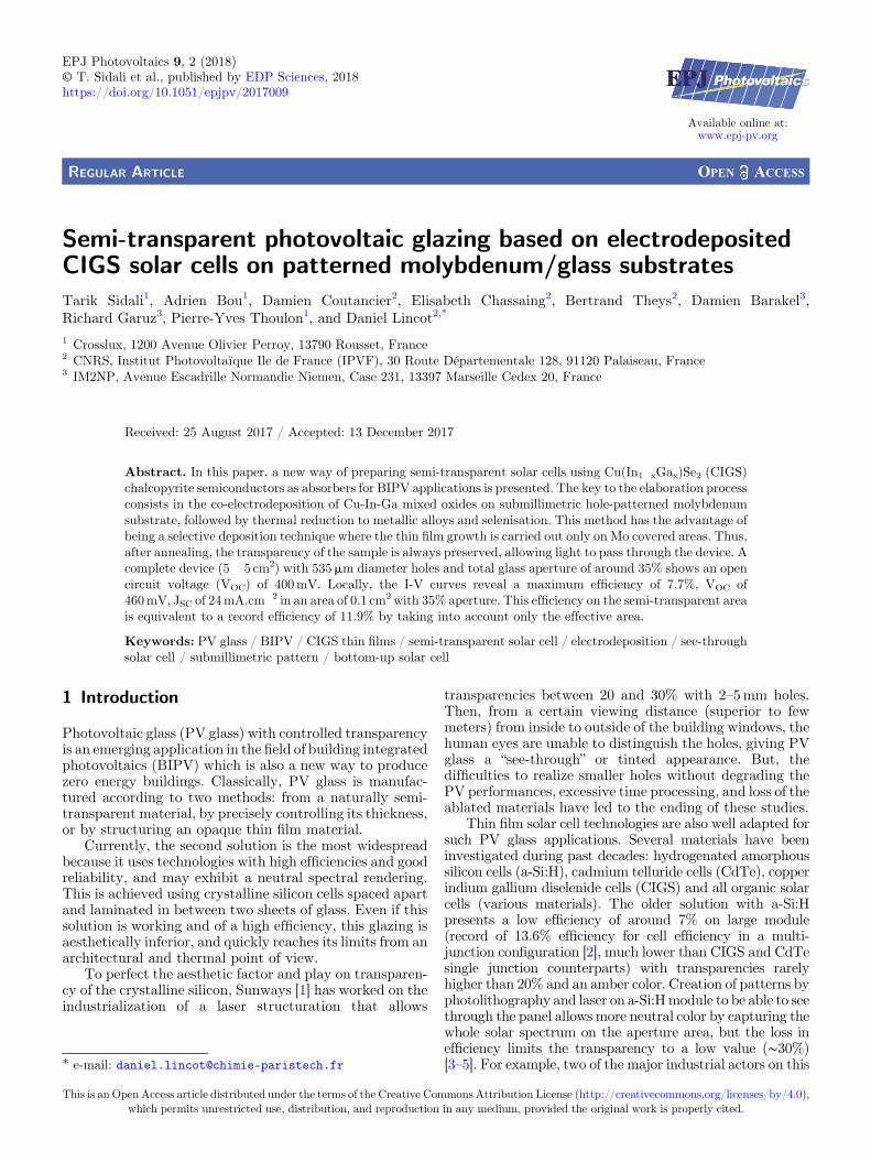
Mo
glass
Mo patterning
Electrodeposition
Hydrogen thermal reduction treatment
Selenization
Cu-In-Ga Cu-In-Ga oxides
Cu(In,Ga)Se2
CdS + ZnO
Fig. 1. Processing steps for the fabrication of semi-transparent CIGS solar cells based on the Glass/patterned Mo/CIGS/CdS/ZnOarchitecture.
2 T. Sidali et al.: EPJ Photovoltaics 9, 2 (2018)
technology, OnyxSolar and PolySolar, announce outputefficiencies around 3% at 30% of transparency.
The CdTe technology has the advantage to have a higherefficiency than a-Si:H (around 22% in cell [2] and 18.6% inindustrial module [6]). CdTe can be deposited as semi-transparent thin film or be structured when deposited as athicker opaque film. For example, PolySolar presentsefficiencies between 7 and 8% for solar windows with avisible light transmission of 30% [4]. The problem of thetoxicity of cadmium remains a drawback to the deploymentof CdTe in buildings. CIGS presents record cell efficienciesup to 22.6% [7], even higher than CdTe, with moduleefficiencies comparable to CdTe at about 18% [8]. The CIGStechnology has the advantage to be able to work withminuteamount of cadmium (30–50nm CdS buffer layer) as used inthe record cell and by several module manufacturers, andmore and more without cadmium by the progressivesubstitution of CdS buffer layers by ZnS based buffer layers,in particular by the leading industrial manufacturer [9].
Finally, the organic solution, by using low cost materialsand production methods (roll-to-roll) at low thicknesses(<500 nm for the whole stack), allows homogeneoustransparencies by playing simply on the thicknesses of thedifferent materials. Nevertheless, from an industrial point ofview, this solution is not yet mature and still presentslimitations due to lifespan and efficiency (record of 12–13%in cell [2], in strong evolution since 2007).
The CIGS technology is very promising for enteringinto this PV glass field since it can deliver high efficiencysolar cells (22.6% record) or modules and already exists inthe market for power applications. This is why the use ofCIGS, a long lifespan and high efficiency technology, is avery adequate solution for semi-transparent PV glazingand is the object of our study. Nevertheless, existingstructuration approaches remain limited to drilling holes inthe whole stack at the end of the module manufacturingprocess, with difficulties to achieve submillimetric pat-terns, limiting the flexibility of the process, the quality ofthe visual rendering and the execution speed.
Localized deposition techniques can naturally allowgrowth on defined areas without masking. Such self-alignedgrowth techniques include electrodeposition or ink pro-
cesses. In this study, we chose electrodeposited solar cells.Electrodeposition, which has already been proven to be anefficient industrial method for standard modules, allowsefficiencies up to 14% [10] in module and 17.3% in cell. Byadopting bottom-up solar cell synthesis via localizedgrowth processes, we have the advantage of drasticallylimiting raw material consumption, in comparison withapproaches based on post-deposition patterning. This is ofcrucial importance to limit the price of the final PV glassand also in the perspective of improving the environmentalimpact by limiting the use of rare elements (indium andgallium).We also have the possibility to reduce the patternsize largely under the millimeter without degrading the PVperformance. This approach has been recently successfullystudied for CIGS electrochemical deposition on onemillimeter wide molybdenum lines in view of CIGSmicrocell applications under concentration [11].
The objective of this paper is to describe our electro-deposited bottom-up solar cell synthesis on laser-struc-tured glass/molybdenum substrates with submillimeterhole patterns fully compatible with see-through PVwindows for BIPV application.
2 Experimental methods
The approach to create glass aperture in the classical glass/Mo/CIGS/buffer/ZnO/AZO structure is to start from alaser patterned Mo back contact (900 nm deposited by DCsputtering), and selectively deposit the CIGS layer only onthe Mo covered areas (Fig. 1). A key method allowing suchselective deposition of CIGS is electrodeposition. Electro-deposited CIGS solar cells have been prepared in theclassical configuration on glass/Mo substrate using anelectrodeposition route introduced recently in the field, andknown as the oxide route [12]. It consists in depositing alayer of mixed copper, indium and gallium oxides/hydroxides by cathodic deposition from an aqueoussolution of nitrate salts. Then the oxides are reduced tometals through hydrogen thermal treatment, followedby selenisation to form CIGS (Fig. 1). A record efficiencyof 12.4% [13] has been obtained with mean values around

(a) (b)
Fig. 2. (a) Glass/Mo substrate (5� 5 cm2) with laser patterned Mo back contact zone (4� 4 cm2) in the center after theelectrodeposition of CIGS. (b) SEM details of the structured Mo surface with conformal CIGS cells giving the size of the holes of thepattern.
T. Sidali et al.: EPJ Photovoltaics 9, 2 (2018) 3
11% [14]. This process has been adapted for the depositionon patterned Mo substrates. The deposition have beencarried out in an aqueous electrolyte at room temperaturecontaining 13mM of copper(II) nitrate, 20mM of indiumnitrate and 10mM of gallium nitrate, acidified by nitricacid addition (pH 1.8). The bath composition was chosen tolead to molar ratios Cu/(In+Ga) and Ga/(Ga+ In) ofabout 0.9 and 0.3, respectively to lead to good qualityabsorbers. The electrochemical set up was Biologic VSPpotentiostat operating in the three electrode configurationat a fixed applied potential versus a calomel referenceelectrode. Typical patterns are ∼535mm diameter holeswith ∼775mm spacing, leading to ∼240mm wide Mochannels at minimum (Fig. 2) and total glass aperture of∼35%. The solar cells are completed by the deposition of50 nm of CdS buffer layer by chemical bath deposition, anda window layer composed of 80 nm intrinsic ZnO and400 nm Al-doped ZnO by RF sputtering. Optoelectronicproperties of devices were determined by current–voltagecharacteristics measured under standard AM 1.5G con-ditions using an AAA class solar simulator (Newport); ahomemade spectral response (EQE) setup was used todetermine the short circuit current in full and semi-transparent areas of the device. Photocurrent mapping hasbeen realized by means of specific LBIC equipmentdedicated to large area studies and developed in theframework of the Equipex ANR project called DURASOL.This homemade LBIC can perform large-scale photocur-rent mappings (1.7m� 1.2m, resolution: 1mm) as well assmall-scale photocurrent mappings (1mm� 1mm, resolu-tion: 10mm). The light source is a polychromatic whitelight but it can also be monochromatic in the visible rangefrom 400 to 1200 nm. In this work, the mappings wereobtained with the white light and the small scale and high-resolution mode has been used.
3 Results and discussion
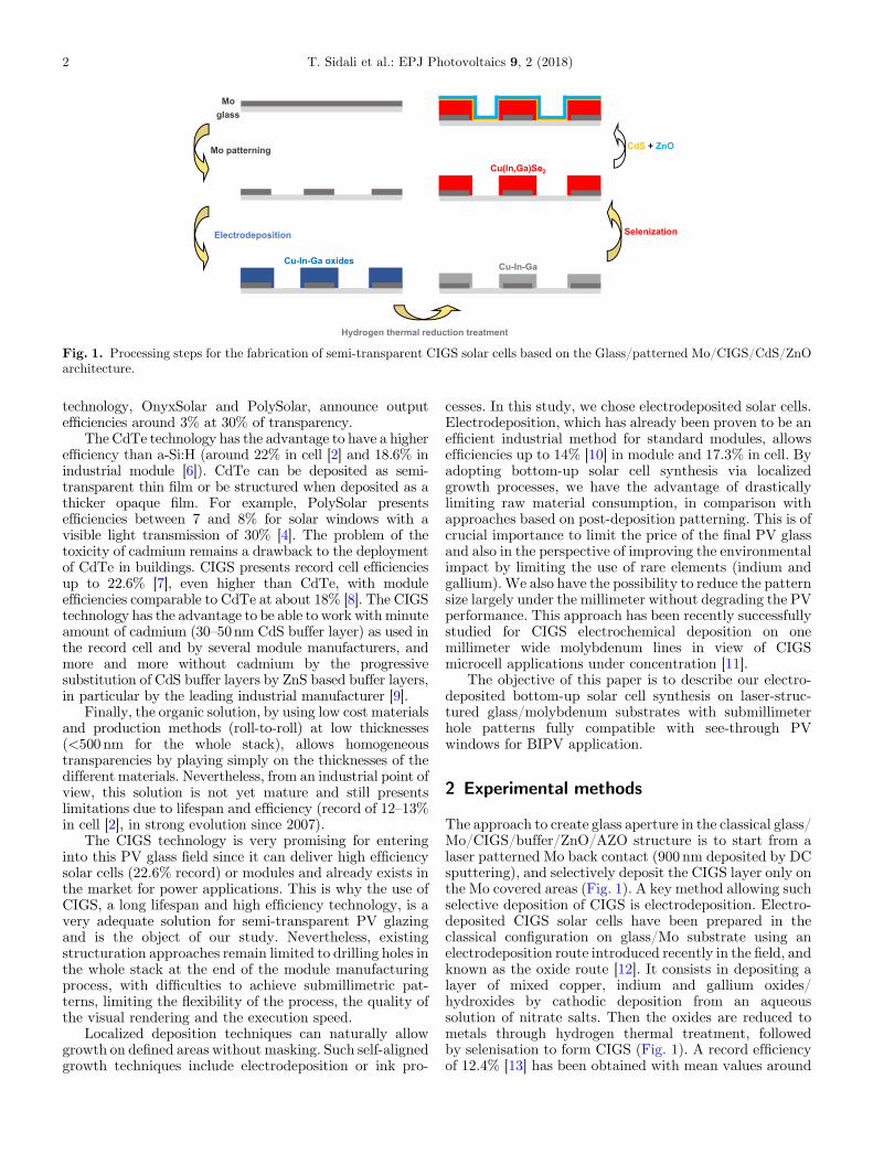
We succeeded in obtaining conformal deposits of CIGS onthe patterned Glass/Mo substrates as shown in Figures 2and 3. Figure 3 shows the surface morphology at thedifferent steps of the production of the CIGS layer.
Globally, we can note that the pattern size is preserved ineach step validating the bottom-up technique on submilli-meter patterns. The SEM images, presented in Figure 3a,show that the patterned Mo is completely covered by theCu-In-Ga oxide/hydroxide precursor film. No depositioninside the holes can be observed; thereby the transparencyof the device is preserved. The deposition is homogeneouswith some cracks resulting from partial dehydration of thefilm. The composition will allow obtaining good perfor-mance of CIGS with Cu/(In+Ga) and Ga/(In+Ga)ratios of 0.77 and 0.34, respectively. Differences areobserved with the deposition on plain Mo substrates sincethe diffusion regimes from the solution are different [11],requiring some adjustment in the deposition parameters.After reduction heat treatment under flowing purehydrogen (Fig. 3b), again, no deposition is observedinside the holes. The precursor has a metallic aspect,which is confirmed by XRD with the formation of metallicindium and a metallic alloy of CuInGa [14]. The CGI andGGI ratios, around 0.84 and 0.30, respectively, change alittle bit, probably due to loss of indium by evaporationduring annealing. After selenisation (Fig. 3c), thetransparency of the sample is also preserved with nodeposition inside the holes. The XRD analysis shows twophases: CIS on the top and CIGS [14] with a GGI ratio of0.25. This explains the decrease in the GGI ratio probablyrelated to the gallium diffusion at the back contact duringthis annealing step [14]. We can note that this gradientwith an increase of gallium towards the Mo contact is verybeneficial to the cell performances.
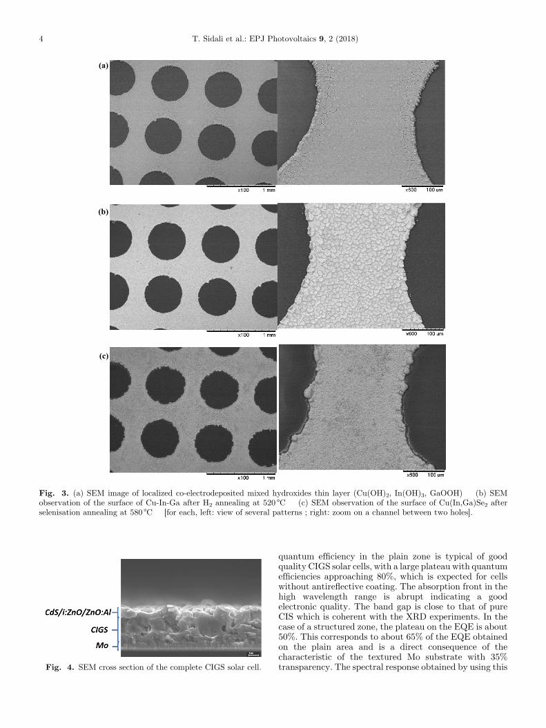
Figure 4 presents SEM cross section of the completeCIGS solar cell in full area between holes. The CIGSthickness is about 2.6mm with large grains near the frontcontact and small grains near the molybdenum backcontact which is due to the gallium diffusion [14].
Solar cells characterizations were performed to deter-mine the PV properties. On Figure 5, a photograph isshown of a 5� 5 cm2 sample with a Ni/Al contacting gridwith 5mm distance between the lines.
This configuration allows carrying out spectral responsemeasurements on localized zones of the substrate usingmodulated illumination. Figure 6 shows spectral responsemeasurements on a patterned zone and on a plain one. The
(a)
(b)
(c)
Fig. 3. (a) SEM image of localized co-electrodeposited mixed hydroxides thin layer (Cu(OH)2, In(OH)3, GaOOH) � (b) SEMobservation of the surface of Cu-In-Ga after H2 annealing at 520 °C � (c) SEM observation of the surface of Cu(In,Ga)Se2 afterselenisation annealing at 580 °C � [for each, left: view of several patterns ; right: zoom on a channel between two holes].
Fig. 4. SEM cross section of the complete CIGS solar cell.
4 T. Sidali et al.: EPJ Photovoltaics 9, 2 (2018)
quantum efficiency in the plain zone is typical of goodquality CIGS solar cells, with a large plateau with quantumefficiencies approaching 80%, which is expected for cellswithout antireflective coating. The absorption front in thehigh wavelength range is abrupt indicating a goodelectronic quality. The band gap is close to that of pureCIS which is coherent with the XRD experiments. In thecase of a structured zone, the plateau on the EQE is about50%. This corresponds to about 65% of the EQE obtainedon the plain area and is a direct consequence of thecharacteristic of the textured Mo substrate with 35%transparency. The spectral response obtained by using this

(a)
(b)
Fig. 5. (a) View of a completed device over the 5� 5 cm2 patterned substrate, with Ni/Al contacting grid deposited on top of the ZnOlayer, (b) and on a part of this sample the preparation of isolated smalls cells with varnish (around 0.1 cm2).
Fig. 6. EQE curves in full (black) and semi-transparent (red)areas.
T. Sidali et al.: EPJ Photovoltaics 9, 2 (2018) 5
correction factor is shown in the figure and superposes wellwith that of the plain substrate. This demonstrates that thePV characteristics of the internal CIGS junction are notaffected by the structuration of the substrate which is animportant information for the relevance of the technology.
The expected photocurrent density under standardAM1.5 1000W/m2 illumination has been calculated by theintegration of quantum efficiencies under the solar spec-trum.This leads, fromFigure 6, to 31.1 and 21.3mA/cm2 forplain and semi-transparent areas respectively.
Figure 7a presents the I-V curves of the complete device(5� 5 cm2) under illumination and in darkness.
The curve under illumination leads to an open circuitpotential of 400mV, a short circuit current around9mA/cm2 and a fill factor of 27%. While the open circuitvoltage is correct, the short circuit current density and thefill factor are much lower than expected, in particular forthe photocurrent. As a consequence the conversionefficiency is very low at the percentage level. A shuntresistance effect can be excluded since the slope on the I-Vcurve in the dark at the origin is much lower than thatunder illumination, corresponding to a shunt resistancevalue about 750V.cm2. On the contrary, the behavior
under illumination fits with a strong series resistance effectwhich is also visible on the I-V curve in dark with the quasilinear variation in the positive polarization domain. To testthis hypothesis, measurements have been carried out onsmall solar cells distributed all over the substrate, withareas around 10mm2 (Fig. 5b). The results are shown inFigure 7b for a series of cells along the width of thesubstrate in a structured Mo zone. It appears that the I-Vcurves are of much better quality with the suppression ofthe strong detrimental series resistance effect. The PVparameters now reach for the best cell a VOC of 460mV, aJSC of 24.4mA/cm2 and a fill factor of 56%. The JSC value isnow consistent with that expected from the spectralresponse analysis. The corresponding efficiency is 7.7%.Taking into account the transparency factor of 35% leadsto an equivalent efficiency on the plain substrate of 11.9%,which is close to the record efficiencies previously obtainedon plain substrates for this process [13,14]. This demon-strates that there are no significant losses due to thestructuration of the molybdenum back contact. This is keyresult for the validity of this approach for high efficiencyPV glazing.
Further experiments have been carried out to map theproperties of the 5� 5 cm2 device and shown in Figure 8.Figure 8a shows an LBIC mapping of the whole devicecorresponding to the conditions of Figure 7a. We canobserve the photocurrent generation on the zones coveredwith CIGS over the whole substrate. However the amplitudeof the LBIC signal is strongly varying from bottom to top.This indicates losses along the vertical direction andconfirms the series resistance effect evidenced from theglobal I-V curve. It can be related to series resistance in theZnO layer and to resistive Ni/Al contact.
Mapping experiments (Fig. 8b) have been made afterthe formation of small isolated cells all over the substrate(Fig. 5b) corresponding to the I-V curves presented inFigure 7b. We can see a much more homogeneous andefficientPV response over thewhole device, with efficienciesbetween about 5% and almost 8%, with good performanceeven in the regions where the LBICmeasurement shows low

Fig. 8. (a) LBIC measurements; (b) mapping of localized efficiencies.
Fig. 7. (a) I-V curves on complete device; (b) localized I-V curves on 0.1 cm2 surfaces with holes.
6 T. Sidali et al.: EPJ Photovoltaics 9, 2 (2018)
collection of electrons. This confirms the high impact of theZnO layer on series resistances over the whole device area.
4 Conclusion
In this paper, we have presented a successful experimentalprocess to prepare semi-transparent solar cells using Cu(In1�xGax)Se2 (CIGS) chalcopyrite semiconductors asabsorber for BIPV applications via electrodeposition onstructured Mo substrates with submillimetric patterns.
We obtained a 7.7% efficiency value for a see-throughsolar cell with 35% of aperture area on glass correspondingto a Mo substrate comprising holes of about 535mm indiameter. This represents an equivalent efficiency of 11.9%for a solar cell on plain substrate, which is similar to thehighest values previously achieved with this process. Thetransparency of the sample is preserved all along theprocess. These first results already represent the proof ofconcept of the electrodeposition approach for PV glazing.Next steps will be the optimization of this concept and theincrease of the sample size (15� 15 cm2) to make anoperational demonstrator device. Moreover, for industrialpurposes, the electrodeposition process has the advantageof nicely scaling to larger device areas (60� 120 cm2 and
beyond), as required for PV windows, which is the currentdevelopment at Crosslux.
This work has been done in the frame of a collaboration contractbetween Crosslux and CNRS at IRDEP. The IRDEP team isacknowledged for its support.We would like to thank Anne-Marie GONCALVES and ArnaudETCHEBERRY from the Institut Lavoisier de Versailles (ILV)for their experimental support.These results have been presented at PVTC 2017 in Marseille andpartially presented at JNPV 2016.
References
1. P. Fath, S. Keller, A. Boueke, R. Kuhn, E. Bucher, inConference Record of the Twenty-Eighth IEEE PhotovoltaicSpecialists Conference � 2000 (Cat. No.00CH37036), IEEE(2000), pp. 335–338
2. Best research-Cell Efficiencies, National Renewable EnergyLaboratory: www.nrel.gov/pv/assets/images/efficiency-chart.png
3. A. Takeoka, S. Kouzuma, H. Tanaka, H. Inoue, K.Murata, M.Morizane, N. Nakamura, H. Nishiwaki, M.Ohnishi, S. Nakano,Y. Kuwano, Sol. Energy Mater. Sol. Cells 29, 243 (1993)

T. Sidali et al.: EPJ Photovoltaics 9, 2 (2018) 7
4. Polysolar, Building Integrated Transparent PhotovoltaicGlass, http://www.polysolar.co.uk
5. ASI Glass, http://www.schott.com/d/france/a753c14e-c34c-4cf3-9289-90c790ec7da1/1.0/schott_asi_glass_brochure_fr.pdf
6. M.A. Green, Y. Hishikawa, W. Warta, E.D. Dunlop, D.H.Levi, J. Hohl-Ebinger, A.W.H. Ho-Baillie, Prog. Photo-voltaics Res. Appl. 25, 668 (2017)
7. P. Jackson, R. Wuerz, D. Hariskos, E. Lotter, W. Witte, M.Powalla, Phys. Status Solidi � Rapid Res. Lett. 10, 583(2016)
8. J. Nam, Y. Kang, D. Lee, J. Yang, Y.-S. Kim, C.B. Mo, S.Park, D. Kim, Prog. Photovoltaics Res. Appl. 24, 175 (2016)
9. K. Rui, Y. Takeshi, A. Shunsuke, H. Atsushi, F.T. Kong, K.Takuya, S. Hiroki, in 2016 IEEE 43th Photovolt. Spec.
Conf. PVSC 2016 Portland(OR) USA, June 2016 (2016),pp. 3–7
10. C. Broussillou, C. Viscogliosi, A. Rogee, S. Angle, P.P. Grand,S. Bodnar, C. Debauche, J.L. Allary, B. Bertrand, C. Guillou,L. Parissi, S. Coletti, in 2015 IEEE 42nd PhotovoltaicSpecialist Conference (PVSC), IEEE (2015), pp. 1–5.
11. A. Duchatelet, K. Nguyen, P.P. Grand, D. Lincot, M. Paire,Appl. Phys. Lett. 109, 253901 (2016)
12. A. Duchatelet, G. Savidand, N. Loones, E. Chassaing, D.Lincot, J. Electrochem. Soc. 161, D3120 (2014)
13. A. Duchatelet, T. Sidali, N. Loones, G. Savidand, E.Chassaing, D. Lincot, Sol. Energy Mater. Sol. Cells 119,241 (2013)
14. T. Sidali, A. Duchatelet, E. Chassaing, D. Lincot, Thin SolidFilms 582, 69 (2015)
Cite this article as: Tarik Sidali, Adrien Bou, Damien Coutancier, Elisabeth Chassaing, Bertrand Theys, Damien Barakel,Richard Garuz, Pierre-Yves Thoulon, Daniel Lincot, Semi-transparent photovoltaic glazing based on electrodeposited CIGS solarcells on patterned molybdenum/glass substrates, EPJ Photovoltaics 9, 2 (2018)