semiconductor detectors an introduction to semiconductor detector physics as applied to particle...
TRANSCRIPT
Semiconductor detectors
An introduction to semiconductor detector physics
as applied to particle physics
Contents
4 lectures – can’t cover much of a huge field
• Introduction
• Fundamentals of operation
• The micro-strip detector
• Radiation hardness issues

Lecture 3 – Microstrip detector
• Description of device• Carrier diffusion
– Why is it (sometimes) good• Charge sharing
– Cap coupling– Floating strips
• Off line analysis• Performance in magnetic field• Details
– AC coupling– Bias resistors– Double sides devices

What is a microstrip detector?
• p-i-n diode
• Patterned implants as strips– One or both sides
• Connect readout electronics to strips
• Radiation induced signal on a strip due to passage under/close to strip
• Determine position from strip hit info
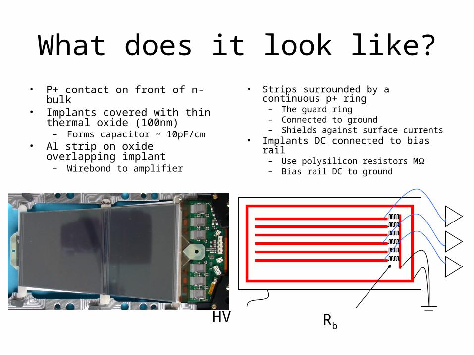
What does it look like?• P+ contact on front of n- bulk• Implants covered with thin thermal
oxide (100nm)– Forms capacitor ~ 10pF/cm
• Al strip on oxide overlapping implant– Wirebond to amplifier
• Strips surrounded by a continuous p+ ring
– The guard ring– Connected to ground– Shields against surface currents
• Implants DC connected to bias rail– Use polysilicon resistors M– Bias rail DC to ground
HV Rb

AC coupled strip detector
HV
Rbias
CAC
Cfeedback

Capacitive coupling
• Strip detector is a RC network
• Cstrip to blackplace = 0.1 x Cinterstrip
• Csb || Cis ignore Csb
• Fraction of charge on B due to track at A:
ACeff
eff
effACis
ACisB
CBA
B
CBA
B
CC
CK
CCC
CCC
CCC
C
QQQ
QK
2 isAC CCas
smallisK
C
CK
CC
AC
is
iseff
A
B
C
ACC
ACC
ACC
isC
isCsQ

Resolution
• Delta electrons– See lecture 2
• Diffusion• Strip pitch
– Capacitive coupling– Read all strips– Floating strips
• Incident Angle• Lorentz force
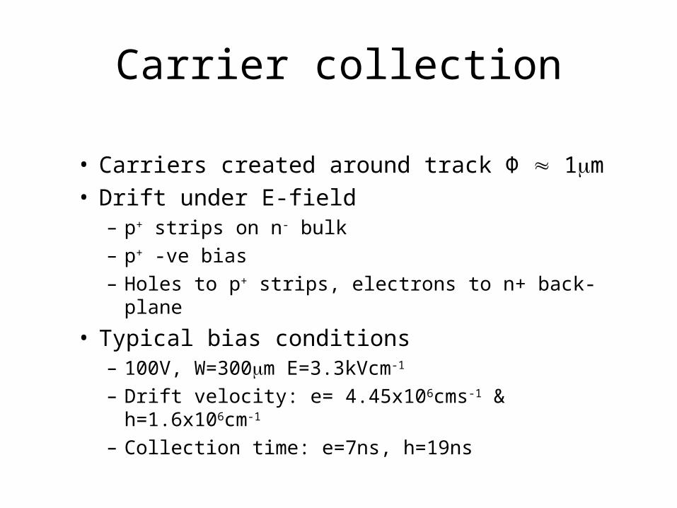
Carrier collection
• Carriers created around track Φ 1m• Drift under E-field
– p+ strips on n- bulk– p+ -ve bias– Holes to p+ strips, electrons to n+ back-plane
• Typical bias conditions– 100V, W=300m E=3.3kVcm-1
– Drift velocity: e= 4.45x10⁶cms-1 & h=1.6x106cm-1
– Collection time: e=7ns, h=19ns

Carrier diffusion
• Diffuse due to conc. gradient dN/dx– Gaussian
• Diffusion coefficient:
• RMS of the distribution:• Since D & tcoll 1/
– Width of distribution is the same for e & h
• As charge created through depth of substrate– Superposition of Gaussian distribution
dxDt
x
DtN
dN
4
exp4
1 2
q
kTD
collDt2
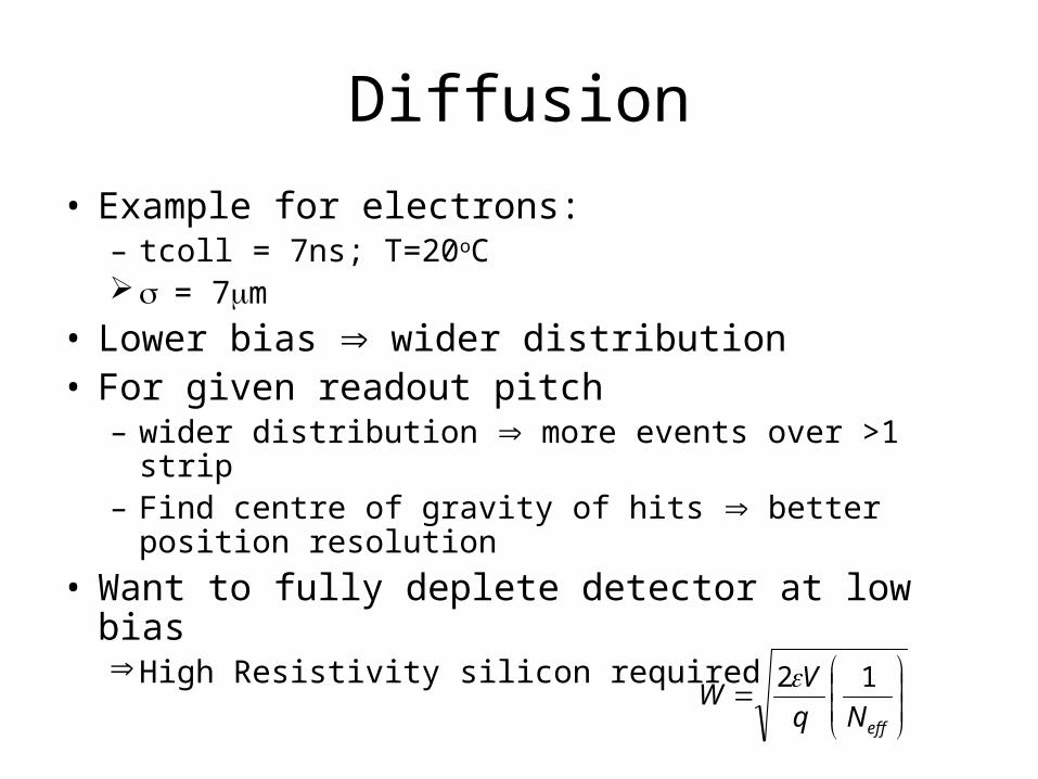
Diffusion
• Example for electrons:– tcoll = 7ns; T=20oC= 7m
• Lower bias wider distribution• For given readout pitch
– wider distribution more events over >1 strip– Find centre of gravity of hits better position
resolution
• Want to fully deplete detector at low biasHigh Resistivity silicon required
effNq
VW
12

Resolution as a f(V)
• V<50V– charge created in undeleted region lost, higher noise
• V>50V– reduced drift time and diffusion width less charge sharing
more single strips
0
1
2
3
4
5
0 20 40 60 80 100
Bias (V)
Res
olu
tio
n (
mic
ros)Spatial
resolution as a function of bias
Vfd = 50V

Resolution due to detector design
• Strip pitch– Very dense– Share charge over many strips– Reconstruct shape of charge and find CofG– Signal over too many strips lost signal (low S/N)
• BUT– FWHM ~ 10m– Technology limited to strip pitch 20m
• Signal on 1 or 2 strips only for normal incident, no B-field
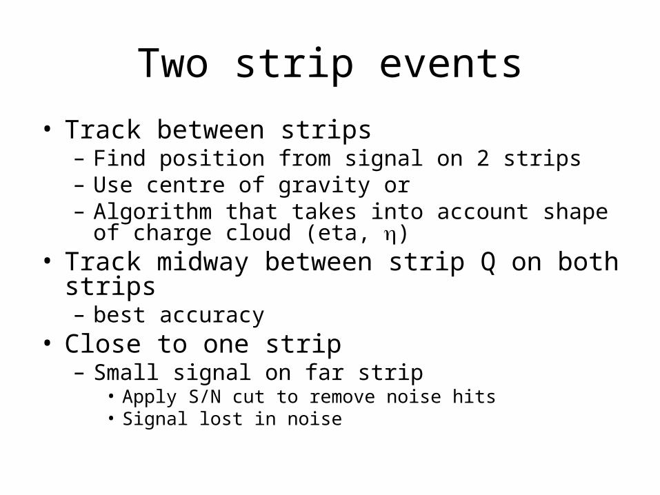
Two strip events
• Track between strips– Find position from signal on 2 strips– Use centre of gravity or– Algorithm that takes into account shape of charge
cloud (eta, )• Track midway between strip Q on both strips
– best accuracy• Close to one strip
– Small signal on far strip• Apply S/N cut to remove noise hits• Signal lost in noise

Off line analysis
• Binary readout– No information on the signal size– Large pitch and high noise
• Get a signal on one strip only
-½ pitch ½ pitch
P(x) <x> = 0
1212
1
)(
)(
21
21
2
21
21
22
Pitch
dxxPx
dxxPxxx

Floating strips
• Large Pitch (60m)
• Intermediate strip
1/3 tracks on both stripsAssume = 2.2m2/3 on single strips = 40/12 = 11.5mOverall:
= 1/3 x 2.2 + 2/3 x 11.5 = 8.4m
60m
20m
20m 20m 20m Capacitive charge coupling2/3 tracks on both stripsNO noise losses due to cap coupling1/3 tracks on single strips = 2/3 x 2.2 + 1/3 x 20/12
= 3.4m
Assume 20m strip pitch = 2.2m

– Have signal on each strip– Assume linear charge sharing between strips
Centre of Gravity
PHL PHR
P
x
stripsii
stripsiii
PH
xPH
X
RL
R
PHPH
PPHX
Q on 2 strips & x = 0 at left strip
e.g. PHL = 1/3PHR
PP
X4
3
4331
43031

Eta function
– Non linear charge sharing due to Gaussian charge cloud shape
PHL PHR
P
x
More signal on RH strip than predicted with uniform charge cloud shape
Non-linear function to determine track position from relative pulseheights on strips

Measure Eta function
• Testbeam with straight tracks
• Reconstruct tracks through detector under test
• Measure deposited charge as a function of incident particle track position

Lorentz force
• Force on carriers due to magnetic force
• Perturbation in drift direction– Charge cloud centre drifts from track position– Asymmetric charge cloud– No charge loss is observed
• Can correct for if thickness & B-field known
E H L
vh
ve
B
c
vEqF
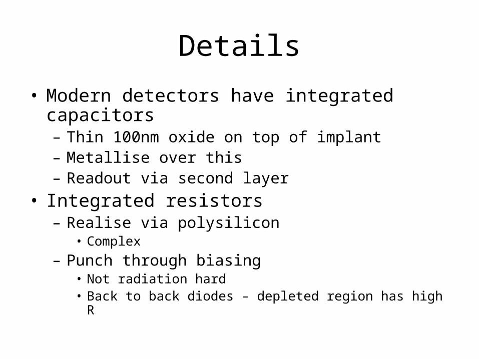
Details
• Modern detectors have integrated capacitors– Thin 100nm oxide on top of implant– Metallise over this– Readout via second layer
• Integrated resistors– Realise via polysilicon
• Complex
– Punch through biasing• Not radiation hard• Back to back diodes – depleted region has high R

Details
• Double sided detectors– Both p- and n-side pattern
• Surface charge build up on n-side– Trapped +ve charge in SiO– Attracts electrons in silicon near surface– Shorts strips together– p+ spray to increase inter-strip resistance