semiconductor detectors for gamma/neutron security imaging · carried out by the detector physics...
TRANSCRIPT

Paul Sellin, Department of Physics
Semiconductor detectors for gamma/neutron security imaging
Paul SellinDepartment of Physics
University of SurreyGuildford, UK
Paul Sellin, Department of Physics
Overview
A summary of two case studies related to security applications, carried out by the Detector Physics group at Surrey:
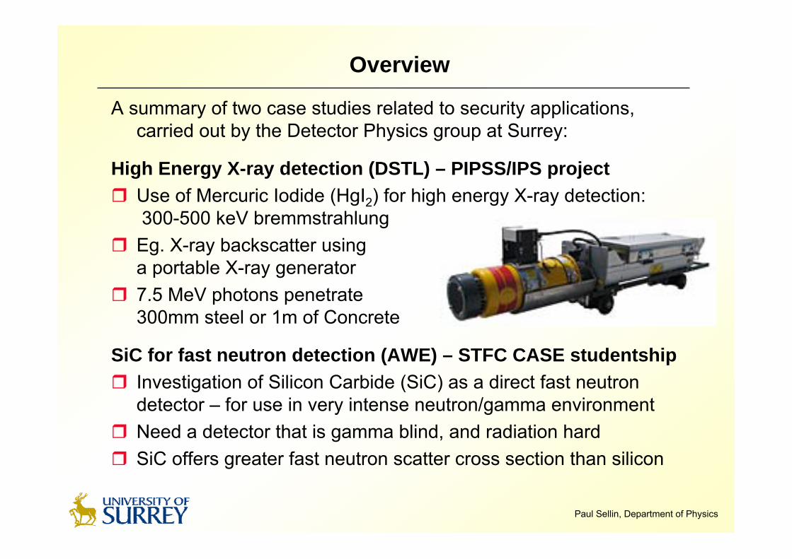
High Energy X-ray detection (DSTL) – PIPSS/IPS project Use of Mercuric Iodide (HgI2) for high energy X-ray detection:
300-500 keV bremmstrahlung Eg. X-ray backscatter using
a portable X-ray generator 7.5 MeV photons penetrate
300mm steel or 1m of Concrete
SiC for fast neutron detection (AWE) – STFC CASE studentship Investigation of Silicon Carbide (SiC) as a direct fast neutron
detector – for use in very intense neutron/gamma environment Need a detector that is gamma blind, and radiation hard SiC offers greater fast neutron scatter cross section than silicon
Paul Sellin, Department of Physics
Some challenges in X-ray Spectroscopy
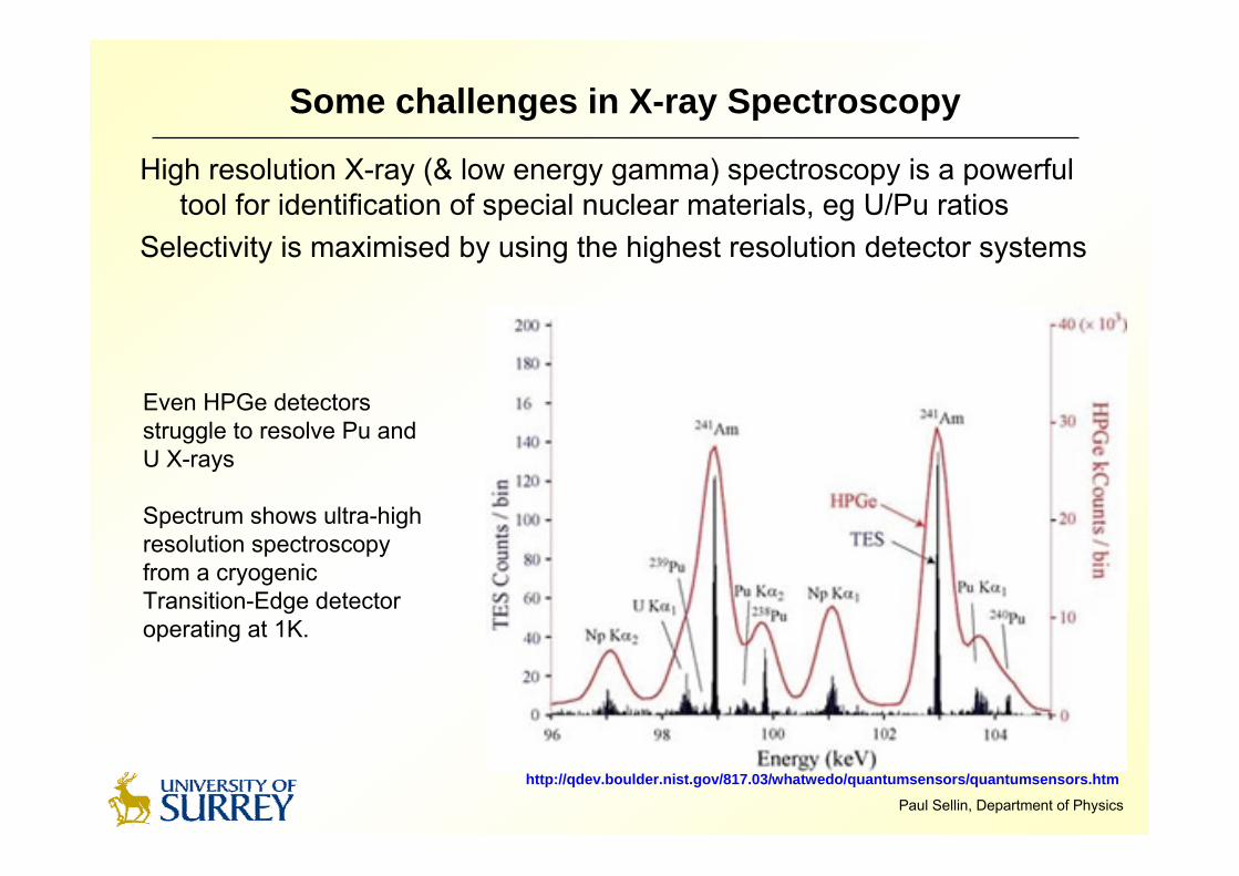
High resolution X-ray (& low energy gamma) spectroscopy is a powerful tool for identification of special nuclear materials, eg U/Pu ratios
Selectivity is maximised by using the highest resolution detector systems
Even HPGe detectors struggle to resolve Pu and U X-rays
Spectrum shows ultra-high resolution spectroscopy from a cryogenic Transition-Edge detector operating at 1K.
http://qdev.boulder.nist.gov/817.03/whatwedo/quantumsensors/quantumsensors.htm

Paul Sellin, Department of Physics
Low energy gammas from Uranium
Typical spectrum from Highly Enriched Uranium (HEU)235U contains a characteristic gamma line at 185 keV, that is resolvable
with a HPGe detector, in the absence of Compton background from higher energy lines
Unfortunately, the backscatter peak from 137Cs is at ~180 keV…

Paul Sellin, Department of Physics
Imaging of gamma rays
Gamma imaging methods are being adopted in security applications, eg. stand-off imaging, which borrow techniques from astronomy and medical imaging applications
Truck-mounted coded aperture imaging arrays are being developed in theUS which combine the imaging of NaI ‘pixel’ detectors with the gamma selectivity of high resolution Ge detectors:
L. J. Mitchell et al, Mobile Imaging and Spectroscopic Threat Identification (MISTI), paper SD1-2, IEEE Nuclear Science
Symposium Dresden 2008

Paul Sellin, Department of Physics
Coded aperture imaging detectors
Key elements of the coded aperture imaging system:1. lead tiles for coded aperture mask2. Ge detector linear area for selectivity (gamma spectroscopy)3. 2D array of NaI detectors for maximum imaging sensitivity4. LN2 dewars for Ge detector cooling
L. J. Mitchell et al, Mobile Imaging and Spectroscopic Threat Identification (MISTI), paper SD1-2, IEEE Nuclear Science
Symposium Dresden 2008

Paul Sellin, Department of Physics
Motivation for high-Z detector materialsMany groups are developing alternative ‘room temperature’ detectors: high detection efficiency at gamma ray energies high Z, ideally >32 room temperature operation wide band gap semiconductor large active volume high quality semiconductor
Photon energy (keV)50 100 150 200 250 300 350 400 450 500
Det
ectio
n E
ffici
ency
(%)
1
10
100
SiGaAsCdTeHgI2TlBr
Calculated for 500m thick material

Paul Sellin, Department of Physics
Semiconductor pixel detectors
There has been a lot of recent activity in transferring bump-bonded pixel detector technology from Silicon to High-Z materials (eg CZT)
Semiconductor pixel detectors providemuch higher spatial resolution thanscintiallator-based imaging arrays
Various groups have developed CZT pixel detector demonstrators eg. 20x20 pixel array, 250m pitch
full spectroscopy 20x10x5 mm pixellated CZT with 300m pixel pitch
CZT
Epoxy on pad
Stud on pad
ASIC
The stud-epoxy flip chip bond process
Surrey and RAL are partners in the Basic Technology ‘HEXITEC’ project to develop fully spectroscopic CZT pixel arrays RAL now has capability for silver-loaded epoxy bump bonding at <300m pitch, which is required for fragile II-VI materials
Paul Sellin, Department of Physics
PIPSS/IPS collaboration with DSTL
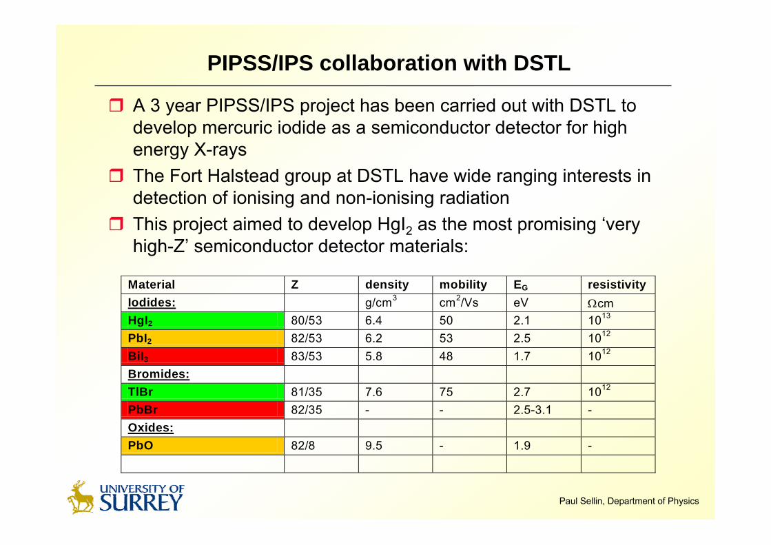
A 3 year PIPSS/IPS project has been carried out with DSTL to develop mercuric iodide as a semiconductor detector for high energy X-rays
The Fort Halstead group at DSTL have wide ranging interests in detection of ionising and non-ionising radiation
This project aimed to develop HgI2 as the most promising ‘very high-Z’ semiconductor detector materials:
Material Z density mobility EG resistivity Iodides: g/cm3 cm2/Vs eV cm HgI2 80/53 6.4 50 2.1 1013 PbI2 82/53 6.2 53 2.5 1012 BiI3 83/53 5.8 48 1.7 1012 Bromides: TlBr 81/35 7.6 75 2.7 1012 PbBr 82/35 - - 2.5-3.1 - Oxides: PbO 82/8 9.5 - 1.9 -

Paul Sellin, Department of Physics
www.realtimeradiography.com
Mercuric Iodide – polycrystalline and single crystalHgI2 is the most promising Z~80 detector material – available as either
single crystal or as a thick-film Thick film HgI2 has been used as an X-ray photoconductor coating for
amorphous silicon X-ray imaging panels – direct coating of polycrystalline HgI2 using low temperature physical vapour deposition
Single crystal HgI2 has much better charge transport properties, and significantly higher energy resolution
HgI2 is a soft material which tends to sublime at room temperature, and special handling is required
single crystal HgI2

Paul Sellin, Department of Physics
Digital pulse shaping with HgI2 detectors
HgI2 shows very low electron and hole mobility, eg ~40 cm2/Vs for electrons
The optimum pulse shaping time is therefore very long, eg. 30sDigital pulse processing methods are used, with software corrections:
137Cs gamma, before correction 137Cs gamma, after correction

Paul Sellin, Department of Physics
High resolution spectroscopy using ‘electron only’electrodes
High quality gamma ray spectrum of single crystal HgI2 using ‘Frisch Grid’ electrodes
L.J. Meng et al, “Spectroscopic Performance of Thick HgI2Detectors”,TNS 53 (2006) 1706-1712

Paul Sellin, Department of Physics
Escape peaks in HgI2All high-Z detectors suffer from photoelectric ‘escape peaks’ – satellite peaks
formed at a fixed energy below the main photopeak due to escape of K-shell X-rays from the detector material:
Hg K-shell energies:
K1 = 68.9 keV (46%)K2 = 70.8 keV (28%)
K1 = 80.2 keV (11%)K2 = 82.5 keV (4%)K3 = 79.8 keV (6%)

Paul Sellin, Department of Physics
Development of a linear array
1.4 mm
0.4 m3.8 m
Schematic top view of the strip detector – 13 strips on 2mm pitch
Cross-sectional view of the HgI2 strip module, mounted on a PCB substrate
The final phase of the project has been to extend the individual HgI2 detector technology to a linear 1D array of ‘short’ strips
The aim is to produce an imaging prototype without the cost of a full 2D pixel array
Detector tests are in progress, eg. with a focussed X-ray or synchrotron beam

Paul Sellin, Department of Physics
Strip detector demonstrator system
We are using the RAL multi-channel spectroscopy NUCAM ASIC which is optimised for low noise X-ray measurements
The motherboard can accommodate up to 4 plug-in detector boards, also suitable for use with CZT detectors

Paul Sellin, Department of Physics
Inelastic neutron imaging
Inelastic neutron scatter imaging is a valuable inspection method for munitions and other special materials.
The emitted gamma ray is characteristic of the chemical species in the item, eg. distinguishing between high explosive, and chemicals such as blister agents and nerve gas
The techniques required a
portable neutron source such as
252Cf, and a high resolution gamma ray spectrometer
Paul Sellin, Department of Physics
Neutron detection for security applications
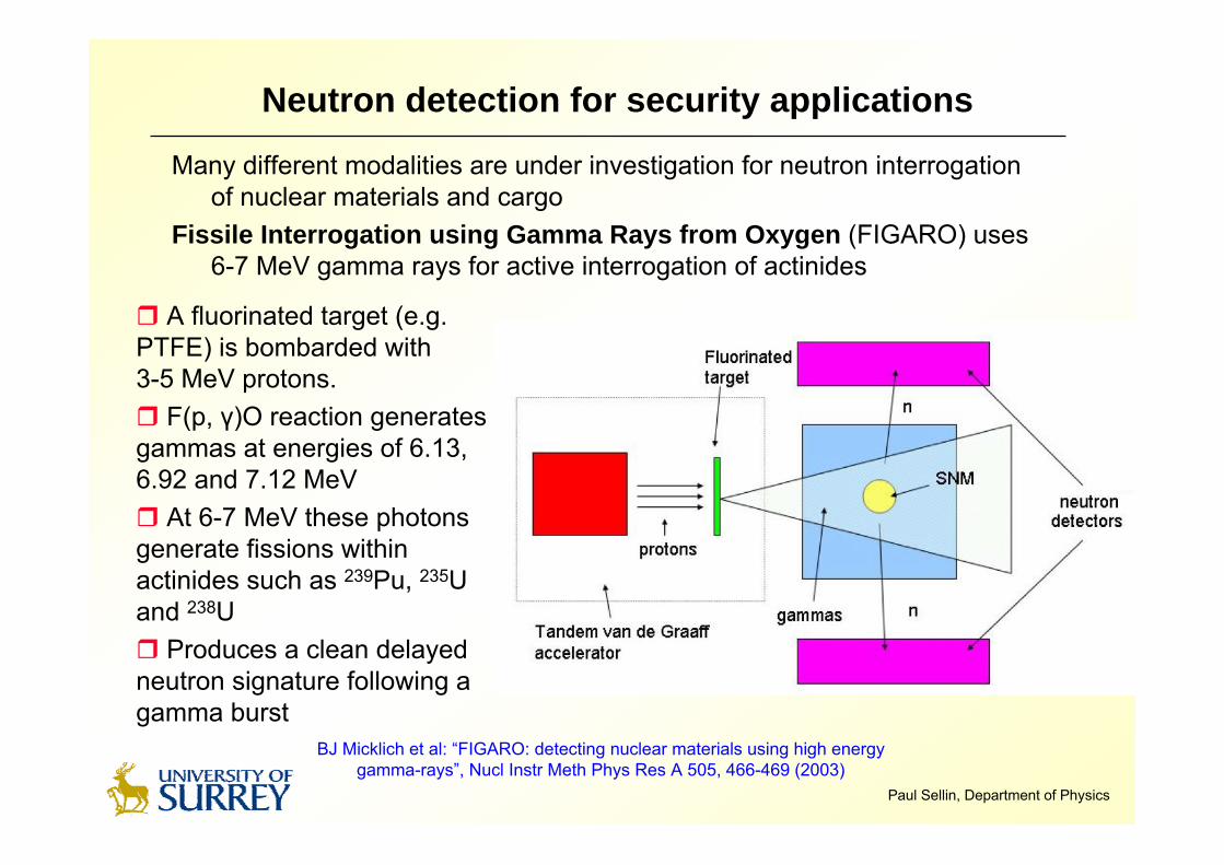
Many different modalities are under investigation for neutron interrogation of nuclear materials and cargo
Fissile Interrogation using Gamma Rays from Oxygen (FIGARO) uses 6-7 MeV gamma rays for active interrogation of actinides
A fluorinated target (e.g. PTFE) is bombarded with 3-5 MeV protons. F(p, γ)O reaction generates gammas at energies of 6.13, 6.92 and 7.12 MeV At 6-7 MeV these photons generate fissions within actinides such as 239Pu, 235U and 238U Produces a clean delayed neutron signature following a gamma burst
BJ Micklich et al: “FIGARO: detecting nuclear materials using high energy gamma-rays”, Nucl Instr Meth Phys Res A 505, 466-469 (2003)

Paul Sellin, Department of Physics
Carbon-based neutron detectors
New semiconductor detector technologies are being developed for fast neutron detection – optimised for high flux environments
The deposited energy from fast neutron elastic scattering is strongly dependent on the mass of the scattering atom:
NMAX EAAE 2)1(
4
For neutron interrogation techniques carbon-based detectors record ~2x more deposited energy than Si
The figure shows the maximum deposited energy for different detector materials, irradiated with 14 MeV neutrons
Paul Sellin, Department of Physics
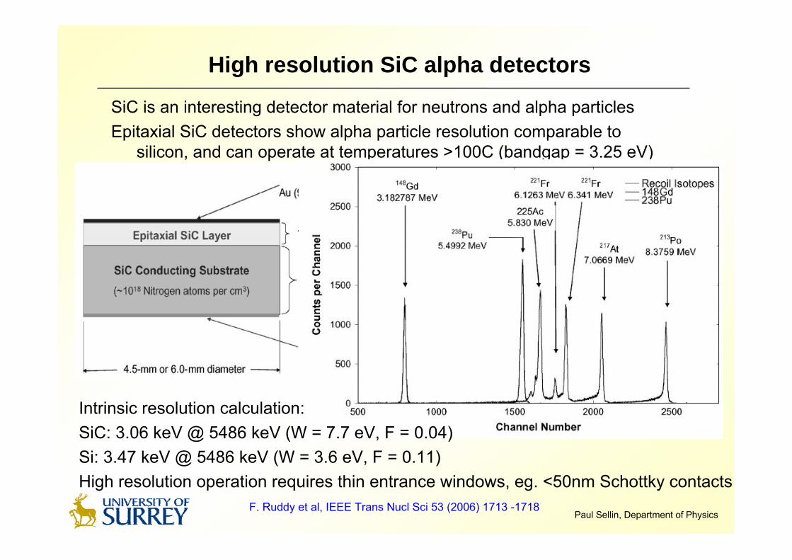
High resolution SiC alpha detectors
SiC is an interesting detector material for neutrons and alpha particlesEpitaxial SiC detectors show alpha particle resolution comparable to
silicon, and can operate at temperatures >100C (bandgap = 3.25 eV)
F. Ruddy et al, IEEE Trans Nucl Sci 53 (2006) 1713 -1718
Intrinsic resolution calculation:SiC: 3.06 keV @ 5486 keV (W = 7.7 eV, F = 0.04)Si: 3.47 keV @ 5486 keV (W = 3.6 eV, F = 0.11)High resolution operation requires thin entrance windows, eg. <50nm Schottky contacts
Paul Sellin, Department of Physics
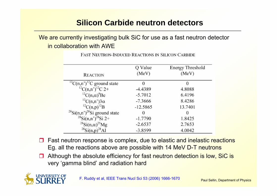
Silicon Carbide neutron detectors
We are currently investigating bulk SiC for use as a fast neutron detectorin collaboration with AWE
Fast neutron response is complex, due to elastic and inelastic reactionsEg. all the reactions above are possible with 14 MeV D-T neutrons
Although the absolute efficiency for fast neutron detection is low, SiC is very ‘gamma blind’ and radiation hard
F. Ruddy et al, IEEE Trans Nucl Sci 53 (2006) 1666-1670

Paul Sellin, Department of Physics
12C(n,)9Be reaction in SiC
Example neutron spectrum from a SiC detector – the dominant peak is the 12C(n,) reaction groundstate at 8.30 MeV
90m thick detector

Paul Sellin, Department of Physics
Conclusions
New developments in gamma and neutron detector technologies are required by security applications
There is considerable potential for knowledge transfer from the High Energy Physics and Nuclear Physics research areas to security problems
High-Z gamma detectors are required for good energy resolution & room temperature operation –CZT and HgI2 continue to develop as promising candidates
Carbon-based detectors such as diamond and SiCoffer good potential for neutron detection in security interrogation applications

Paul Sellin, Department of Physics
Acknowledgements
Our thanks to STFC and to many collaborators who have contributed to this work:
University of SurreyPeter Bryant, Sandeep Chaudhuri,
Annika Lohstroh, Veeramani Perumal
RALPaul Seller, Matthew Veale, Matthew Wilson
DSTLIan Jupp
AWEMark Ellis, John O’Malley, Stacey Robertson