semiconductor industry: how value chain is about...
TRANSCRIPT
© 2010
Copyrights © Yole Développement SARL. All rights reserved.
Semiconductor Industry: How
Value Chain is about to
Change… JC Eloy
CEO, YOLE Développement.
Infineon
Nokia FCI
NXPSTATs ChipPAC
AT&S
© 2010 • 2Copyrights © Yole Développement SARL. All rights reserved.
Yole DeveloppementCompany Presentation
© 2010 • 3Copyrights © Yole Développement SARL. All rights reserved.
Yole Développement
• Yole Développement is a market research and strategy consulting company, founded in 1998 and involved in the following fields:
• MEMS, including microfluidics
• Advanced packaging (3D IC, TSV, SoC, WLP…)
• Power electronics
• LED & HB LED
• Compound semiconductor business (SiC, GaN, AlN, ZnO, Thick SOI…) at substrate and device level
• Photovoltaic, from equipment and materials to cell business
• Our research is performed by in-house personnel conducting open-endeddiscussion based interviews.
• 20 full time analysts with technical and marketing degrees
• Primary research includes over 2,500 interviews annually
• Our customers‟ base and perspectives are global.
© 2010 • 4Copyrights © Yole Développement SARL. All rights reserved.
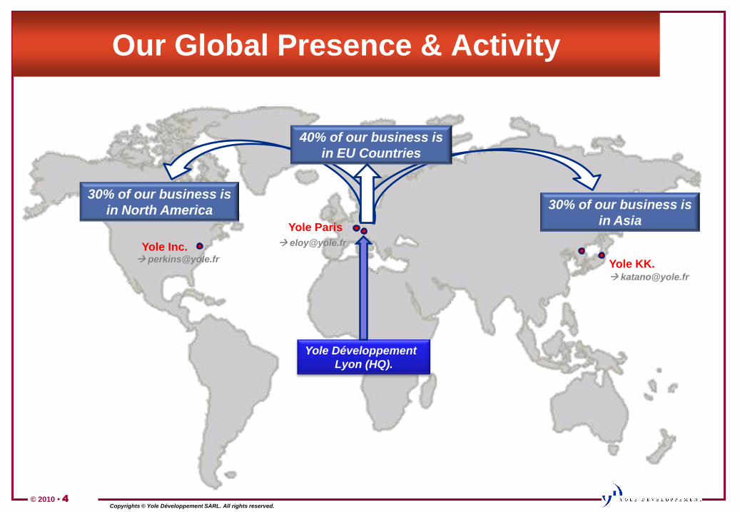
Our Global Presence & Activity
Yole Inc.
Yole Développement
Lyon (HQ).
Yole Paris
Yole KK.
30% of our business is
in North America 30% of our business is
in Asia
40% of our business is
in EU Countries
© 2010 • 5Copyrights © Yole Développement SARL. All rights reserved.
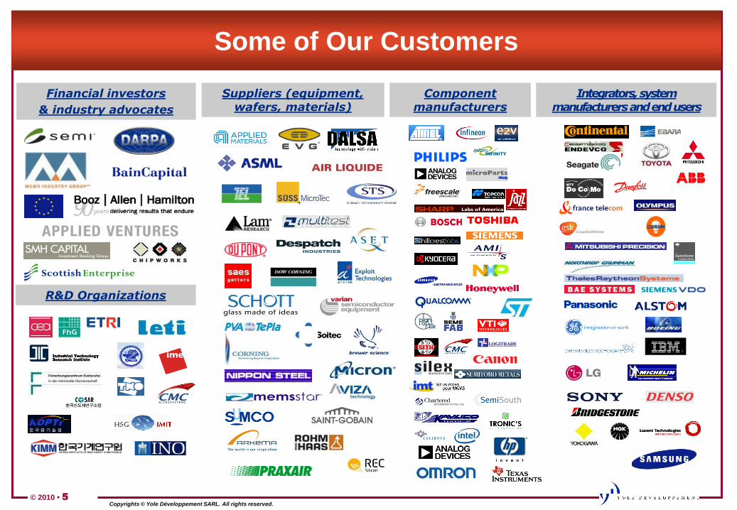
Some of Our Customers
Financial investors
& industry advocates
R&D Organizations
Suppliers (equipment, wafers, materials)
Component manufacturers
Integrators, system manufacturers and end users
© 2010 • 6Copyrights © Yole Développement SARL. All rights reserved.
Custom Analysis Services
• Market research and marketing analysis• Identification of new applications and markets
• Set-up of market segmentation
• Proposal of marketing and action plans
• Strategic analysis• Analysis of positioning to create value
• Development of action plans to improve company performance
• Support in implementation and fund raising
• Technology evaluation• Analysis of technical areas and definition of technology strategy
• Process cost analysis and cost comparison
• Development of product and technology roadmap
• Specific services for investors by Yole Finance• Evaluation and analysis of business plans
• Evaluation of production infrastructure
• Expertise and due diligence before M&A– Company, market and technology expertise
– Strategy, marketing and technical due diligence
© 2010 • 7Copyrights © Yole Développement SARL. All rights reserved.
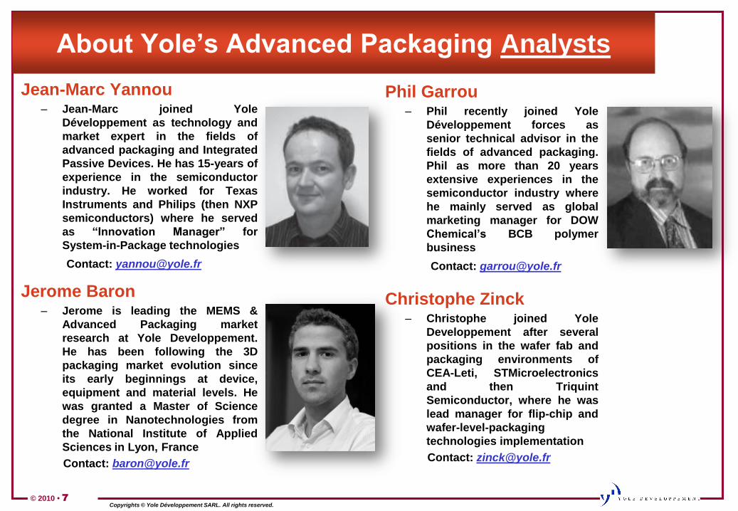
About Yole‟s Advanced Packaging Analysts
Jean-Marc Yannou– Jean-Marc joined Yole
Développement as technology and
market expert in the fields of
advanced packaging and Integrated
Passive Devices. He has 15-years of
experience in the semiconductor
industry. He worked for Texas
Instruments and Philips (then NXP
semiconductors) where he served
as “Innovation Manager” for
System-in-Package technologies
Contact: [email protected]
Jerome Baron– Jerome is leading the MEMS &
Advanced Packaging market
research at Yole Developpement.
He has been following the 3D
packaging market evolution since
its early beginnings at device,
equipment and material levels. He
was granted a Master of Science
degree in Nanotechnologies from
the National Institute of Applied
Sciences in Lyon, France
Contact: [email protected]
Phil Garrou– Phil recently joined Yole
Développement forces as
senior technical advisor in the
fields of advanced packaging.
Phil as more than 20 years
extensive experiences in the
semiconductor industry where
he mainly served as global
marketing manager for DOW
Chemical‟s BCB polymer
business
Contact: [email protected]
Christophe Zinck– Christophe joined Yole
Developpement after several
positions in the wafer fab and
packaging environments of
CEA-Leti, STMicroelectronics
and then Triquint
Semiconductor, where he was
lead manager for flip-chip and
wafer-level-packaging
technologies implementation
Contact: [email protected]

© 2010 • 8Copyrights © Yole Développement SARL. All rights reserved.
Some of Our Customers
Financial investors
& industry advocates
R&D Organizations
Suppliers (equipment, wafers, materials)
Component manufacturers
Integrators, system manufacturers and end users
© 2010 • 9Copyrights © Yole Développement SARL. All rights reserved.
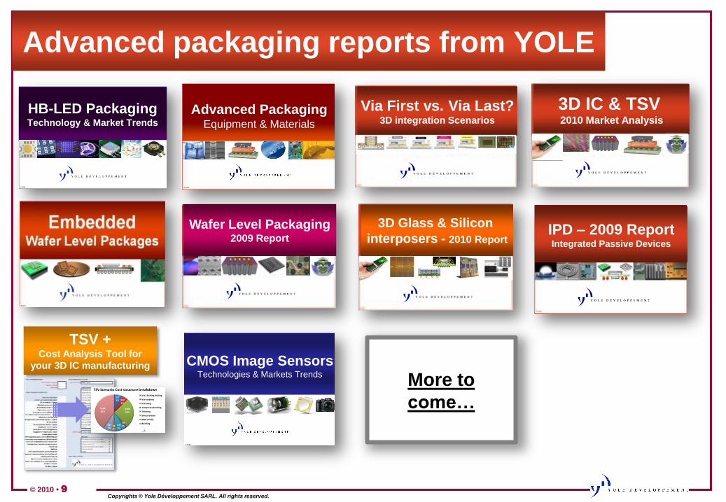
Via First vs. Via Last?3D integration Scenarios
I
M
E
C
S
i
l
e
x
F
r
e
e
s
c
a
l
e
N
o
k
i
a
D
u
P
o
n
t
TSV +Cost Analysis Tool for
your 3D IC manufacturing
3D IC & TSV 2010 Market Analysis
I
M
E
C
S
i
l
e
x
F
r
e
e
s
c
a
l
e
N
o
k
i
a
D
u
P
o
n
t
$27
7% $23
6%
$109
26%
$82%$37
9%$92%
$317%
$168
41%
TSV Scenario Cost structure breakdown
Via / Etching Drilling
Via Isolation
Via filling
Temporary bonding
Thinning
Stress release
BEOL (Pads)
Bonding
IPD – 2009 ReportIntegrated Passive Devices
Wafer Level Packaging2009 Report
N
o
k
i
a
3D Glass & Silicon
interposers - 2010 Report
© 2010
Copyrights © Yole Développement SARL. All rights reserved.
Advanced PackagingEquipment & Materials
NEC-Schott
SUSS Brewer ScienceSTSEVG
DuPont
© 2009
Copyrights © Yole Développement SARL. All rights reserved.
HB-LED Packaging Technology & Market Trends
IR
Osram
© 2010
CMOS Image Sensors Technologies & Markets Trends
BC TechTessera
Chipworks
More to
come…
Advanced packaging reports from YOLE
© 2010 • 10Copyrights © Yole Développement SARL. All rights reserved.
Advanced Packaging
evolutions…
© 2010 • 11Copyrights © Yole Développement SARL. All rights reserved.
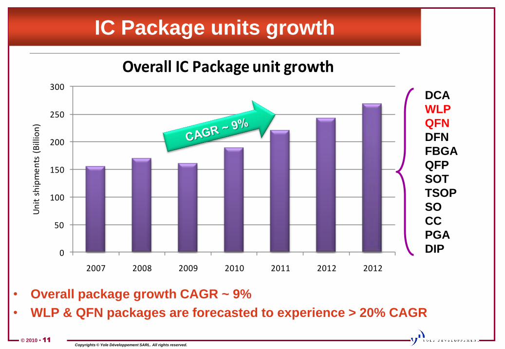
IC Package units growth
• Overall package growth CAGR ~ 9%
• WLP & QFN packages are forecasted to experience > 20% CAGR
0
50
100
150
200
250
300
2007 2008 2009 2010 2011 2012 2012
Un
it s
hip
me
nts
(B
illio
n)
Overall IC Package unit growth
DCA
WLP
QFN
DFN
FBGA
QFP
SOT
TSOP
SO
CC
PGA
DIP
© 2010 • 12Copyrights © Yole Développement SARL. All rights reserved.
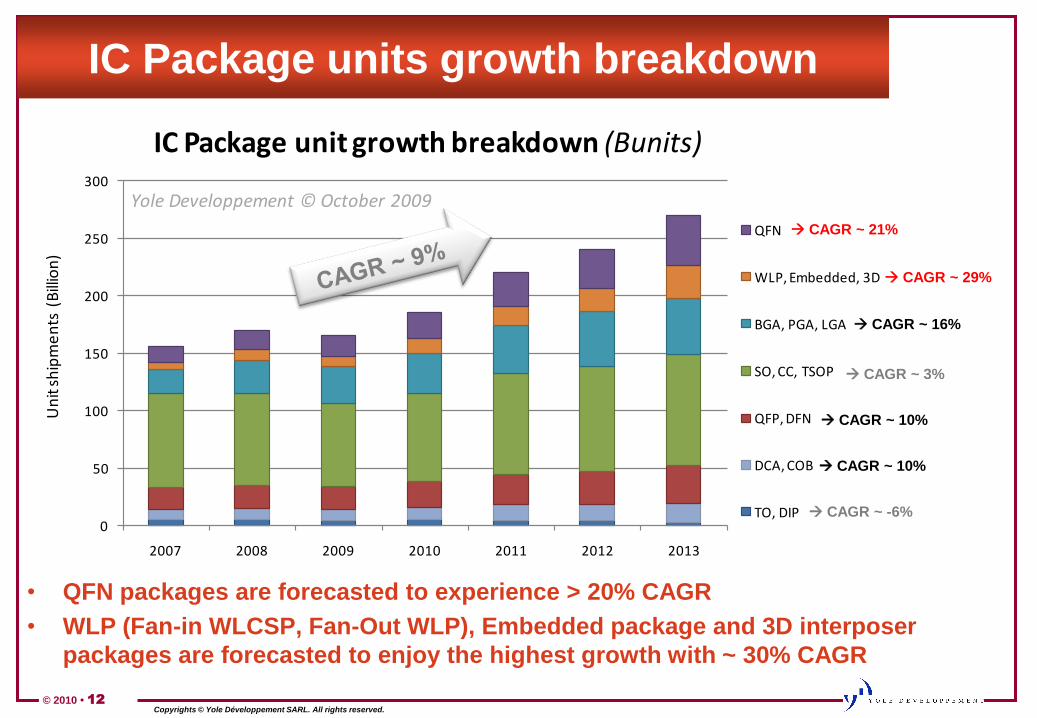
IC Package units growth breakdown
0
50
100
150
200
250
300
2007 2008 2009 2010 2011 2012 2013
Un
it s
hip
me
nts
(B
illio
n)
IC Package unit growth breakdown (Bunits)
QFN
WLP, Embedded, 3D
BGA, PGA, LGA
SO, CC, TSOP
QFP, DFN
DCA, COB
TO, DIP
Yole Developpement © October 2009
CAGR ~ 21%
CAGR ~ 29%
CAGR ~ 16%
CAGR ~ 10%
CAGR ~ 3%
CAGR ~ 10%
CAGR ~ -6%
• QFN packages are forecasted to experience > 20% CAGR
• WLP (Fan-in WLCSP, Fan-Out WLP), Embedded package and 3D interposer
packages are forecasted to enjoy the highest growth with ~ 30% CAGR
© 2010 • 13Copyrights © Yole Développement SARL. All rights reserved.
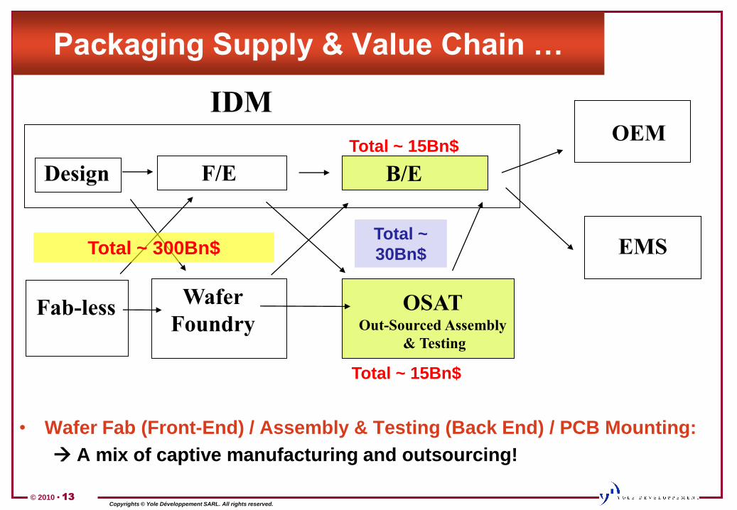
Packaging Supply & Value Chain …
• Wafer Fab (Front-End) / Assembly & Testing (Back End) / PCB Mounting:
A mix of captive manufacturing and outsourcing!
EMS
Wafer
FoundryOSAT
Out-Sourced Assembly
& Testing
IDMOEM
F/E B/E
Fab-less
Total ~ 15Bn$
Total ~ 15Bn$
Design
Total ~ 300Bn$Total ~
30Bn$
© 2010 • 14Copyrights © Yole Développement SARL. All rights reserved.
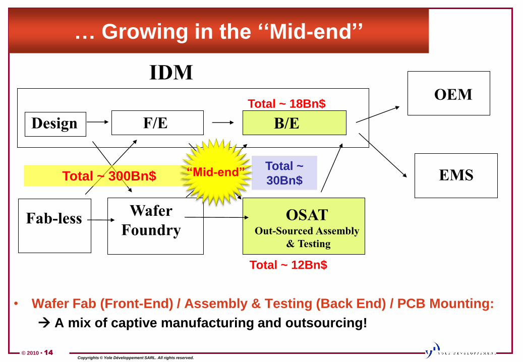
… Growing in the „„Mid-end‟‟
• Wafer Fab (Front-End) / Assembly & Testing (Back End) / PCB Mounting:
A mix of captive manufacturing and outsourcing!
EMS
Wafer
FoundryOSAT
Out-Sourced Assembly
& Testing
IDMOEM
F/E B/E
Fab-less
Total ~ 18Bn$
Total ~ 12Bn$
Design
Total ~ 300Bn$Total ~
30Bn$“Mid-end”
© 2010 • 15Copyrights © Yole Développement SARL. All rights reserved.
MOTHERBOARD &
SUBSTRATE
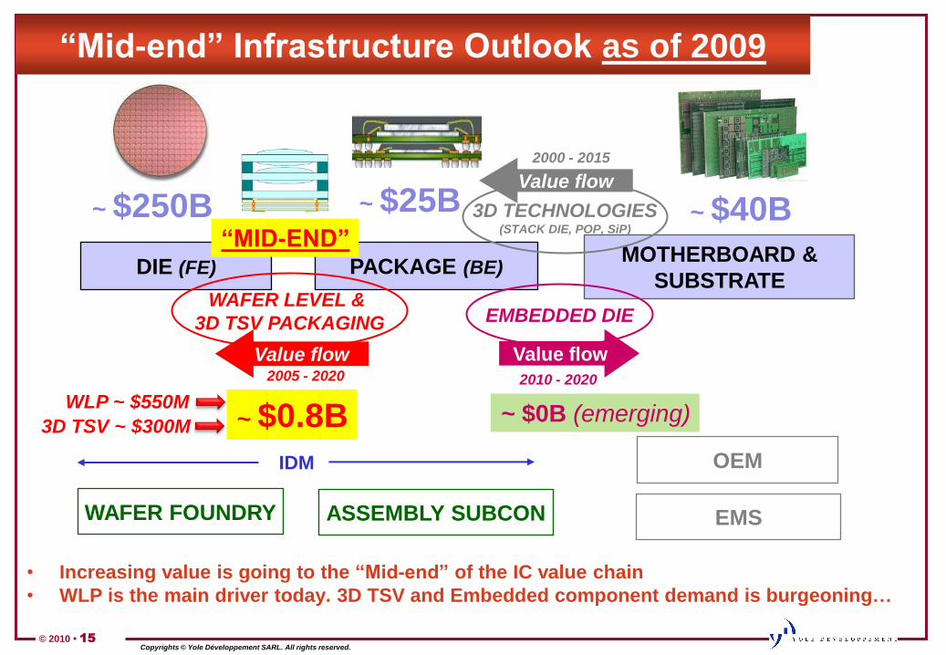
“Mid-end” Infrastructure Outlook as of 2009
DIE (FE) PACKAGE (BE)
WAFER FOUNDRY ASSEMBLY SUBCON
IDM
“MID-END”
EMBEDDED DIE
EMS
OEM
WAFER LEVEL &
3D TSV PACKAGING
Value flow Value flow
3D TECHNOLOGIES(STACK DIE, POP, SiP)
Value flow
2000 - 2015
2010 - 20202005 - 2020
~ $250B ~ $25B
~ $0.8B
~ $40B
~ $0B (emerging)
• Increasing value is going to the “Mid-end” of the IC value chain
• WLP is the main driver today. 3D TSV and Embedded component demand is burgeoning…
WLP ~ $550M
3D TSV ~ $300M
© 2010 • 16Copyrights © Yole Développement SARL. All rights reserved.
MOTHERBOARD &
SUBSTRATE
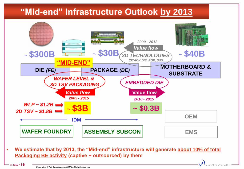
“Mid-end” Infrastructure Outlook by 2013
DIE (FE) PACKAGE (BE)
WAFER FOUNDRY ASSEMBLY SUBCON
IDM
“MID-END”
EMBEDDED DIE
EMS
OEM
WAFER LEVEL &
3D TSV PACKAGING
Value flow Value flow
3D TECHNOLOGIES(STACK DIE, POP, SiP)
Value flow
2000 - 2012
2010 - 20152005 - 2015
~ $300B ~ $30B
~ $3B
~ $40B
~ $0.3B
• We estimate that by 2013, the “Mid-end” infrastructure will generate about 10% of total
Packaging BE activity (captive + outsourced) by then!
WLP ~ $1.2B
3D TSV ~ $1.8B
© 2010 • 17Copyrights © Yole Développement SARL. All rights reserved.
MOTHERBOARD &
SUBSTRATE
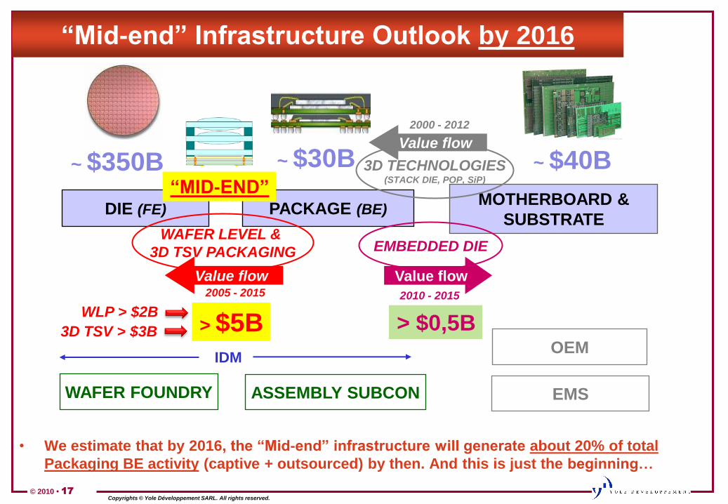
“Mid-end” Infrastructure Outlook by 2016
DIE (FE) PACKAGE (BE)
WAFER FOUNDRY ASSEMBLY SUBCON
IDM
“MID-END”
EMBEDDED DIE
EMS
OEM
WAFER LEVEL &
3D TSV PACKAGING
Value flow Value flow
3D TECHNOLOGIES(STACK DIE, POP, SiP)
Value flow
2000 - 2012
2010 - 20152005 - 2015
~ $350B ~ $30B
> $5B
~ $40B
> $0,5B
• We estimate that by 2016, the “Mid-end” infrastructure will generate about 20% of total
Packaging BE activity (captive + outsourced) by then. And this is just the beginning…
WLP > $2B
3D TSV > $3B
© 2010 • 18Copyrights © Yole Développement SARL. All rights reserved.
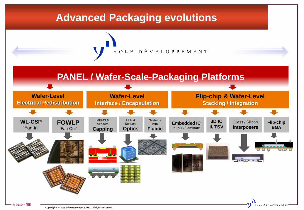
Advanced Packaging evolutions
PANEL / Wafer-Scale-Packaging Platforms
Wafer-Level Electrical Redistribution
Wafer-Level Interface / Encapsulation
Flip-chip & Wafer-LevelStacking / Integration
WL-CSP„Fan-in‟
FOWLP„Fan-Out‟
MEMS &
Sensors
Capping
Systems
with
Fluidic
Glass / Silicon
interposersFlip-chip
BGA
3D IC
& TSVEmbedded IC in PCB / laminate
Courtesy of DALSA
LED &
Sensors
Optics
© 2010 • 19Copyrights © Yole Développement SARL. All rights reserved.
FOCUS ON FAN OUT WLP AND
EMBEDDED DIE.
© 2010 • 20Copyrights © Yole Développement SARL. All rights reserved.
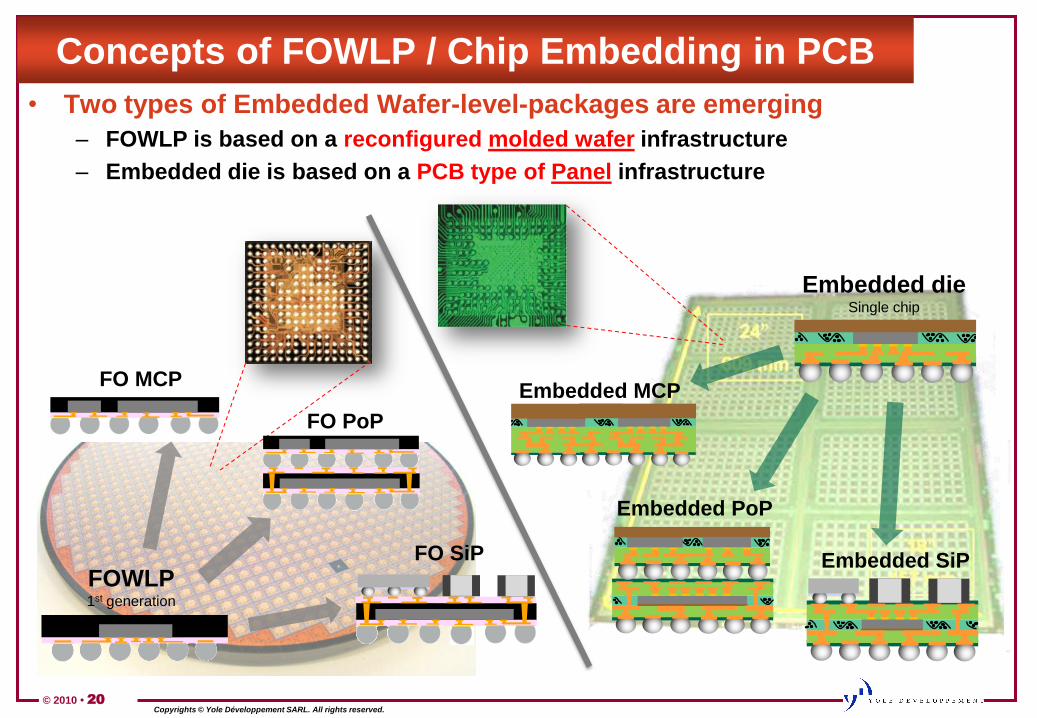
Concepts of FOWLP / Chip Embedding in PCB
• Two types of Embedded Wafer-level-packages are emerging
– FOWLP is based on a reconfigured molded wafer infrastructure
– Embedded die is based on a PCB type of Panel infrastructure
FOWLP1st generation
Embedded dieSingle chip
Embedded SiP
Embedded PoP
FO MCP
FO SiP
FO PoP
Embedded MCP
© 2010 • 21Copyrights © Yole Développement SARL. All rights reserved.
CSR
WLP preparationCu pads + Wafer Test + Wafer
Thinning / Polishing
Supply Chain for Embedded Chip Packaging
OEMsBalling &
Board level Test
AT&S (AT) production line by Q3-2010
Casio Micronics (JP)
Imbera / Daeduck (FI / KR) production line by Q2-2010
Ibiden (JP)
Taiyo Yuden (JP)
Flip-Chip International (US)
SMT / SiPModule integrators
CMK (JP) Murata
Toshiba
NSCNXP
UTAC / NEPES (SG / KR)
Dyconex (Swiss) pilot line ready
Renesas / NEC
TIInfineon
Maxim ICDenso
STEricsson
SEMCO (KR) production line in qualification
Chip Embedding
process
BE stepsMarking, Dicing, inspection,
Tape & Reel
Samsung
Epcos -TDK (GE / JP) pilot line ready
OKI Printed Circuits (JP)
Compass technology (China)
NEC (JP)
Dialog Semi
Bosch
PanasonicNEC Toppan (JP) Casio
CireTec (FR)
STMicro
QualcommVTI
IPS (US)
Fujitsu
Sony
ADI
Thalesams
ASE (TW)
Schweizer Electronic (GE)
Nokia
Pana
sonic
LG
Seagate
ContinentalAmkor (KR)Toyota
Seurin
Medtronic
Motorola
Clover Electronics (JP)
StatsChipPAC (SG)
SPIL (TW)
DNP (JP)
Samsung
© 2010 • 22Copyrights © Yole Développement SARL. All rights reserved.
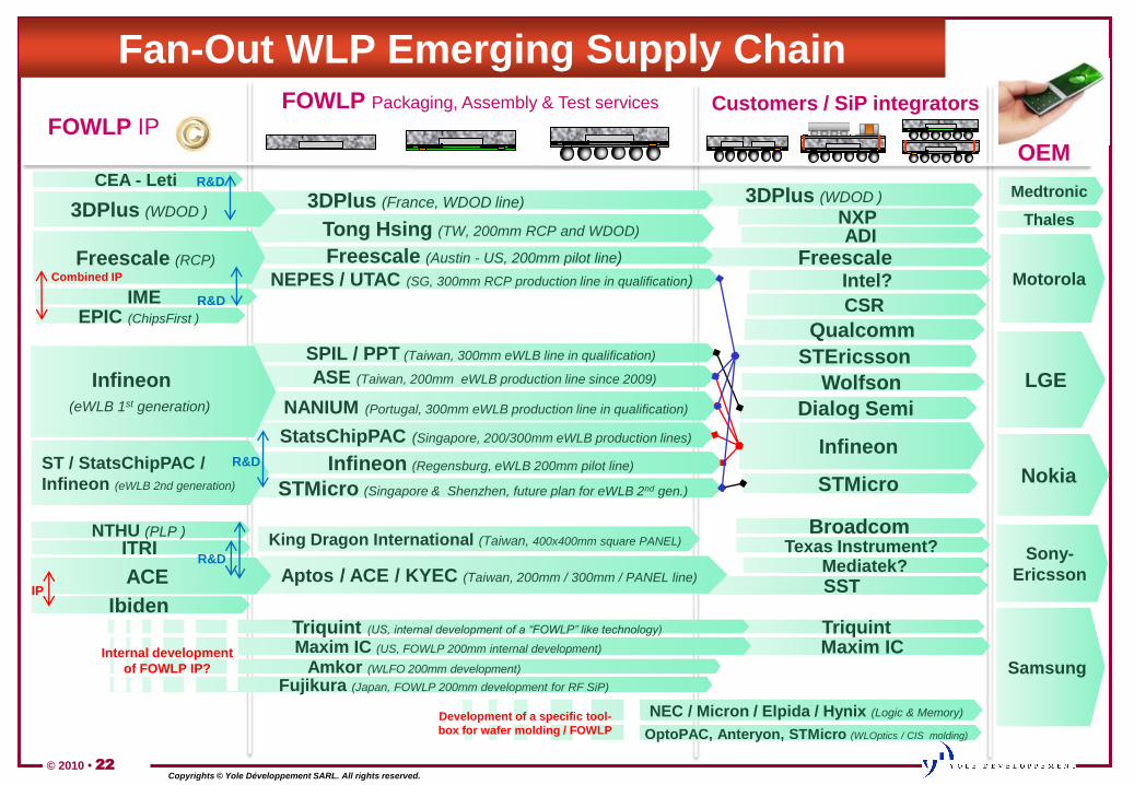
Tong Hsing (TW, 200mm RCP and WDOD)
3DPlus (WDOD )3DPlus (France, WDOD line)
STMicro
Mediatek?
SST
Nokia
Samsung
LGE
Infineon
Freescale
NANIUM (Portugal, 300mm eWLB production line in qualification) Dialog Semi
Wolfson
ADI
STEricsson
Fan-Out WLP Emerging Supply Chain
StatsChipPAC (Singapore, 200/300mm eWLB production lines)
SPIL / PPT (Taiwan, 300mm eWLB line in qualification)
FOWLP IPOEM
ITRI
Aptos / ACE / KYEC (Taiwan, 200mm / 300mm / PANEL line)
IME
Customers / SiP integrators
ASE (Taiwan, 200mm eWLB production line since 2009)
NEC / Micron / Elpida / Hynix (Logic & Memory)
Triquint
NEPES / UTAC (SG, 300mm RCP production line in qualification)
FOWLP Packaging, Assembly & Test services
EPIC (ChipsFirst )
Infineon (Regensburg, eWLB 200mm pilot line)
ACE
Infineon
(eWLB 1st generation)
Freescale (Austin - US, 200mm pilot line) Freescale (RCP)
Ibiden
Intel?
CSR
STMicro (Singapore & Shenzhen, future plan for eWLB 2nd gen.)
ST / StatsChipPAC /
Infineon (eWLB 2nd generation)
Motorola
Sony-
Ericsson
Texas Instrument?
OptoPAC, Anteryon, STMicro (WLOptics / CIS molding)
Combined IP
IP
R&D
R&D
R&D
Development of a specific tool-
box for wafer molding / FOWLP
NTHU (PLP )
3DPlus (WDOD )
CEA - Leti R&D
King Dragon International (Taiwan, 400x400mm square PANEL)
Amkor (WLFO 200mm development)
Qualcomm
Broadcom
Maxim ICMaxim IC (US, FOWLP 200mm internal development)
Fujikura (Japan, FOWLP 200mm development for RF SiP)
Triquint (US, internal development of a “FOWLP” like technology)
Internal development
of FOWLP IP?
Medtronic
ThalesNXP
© 2010 • 23Copyrights © Yole Développement SARL. All rights reserved.
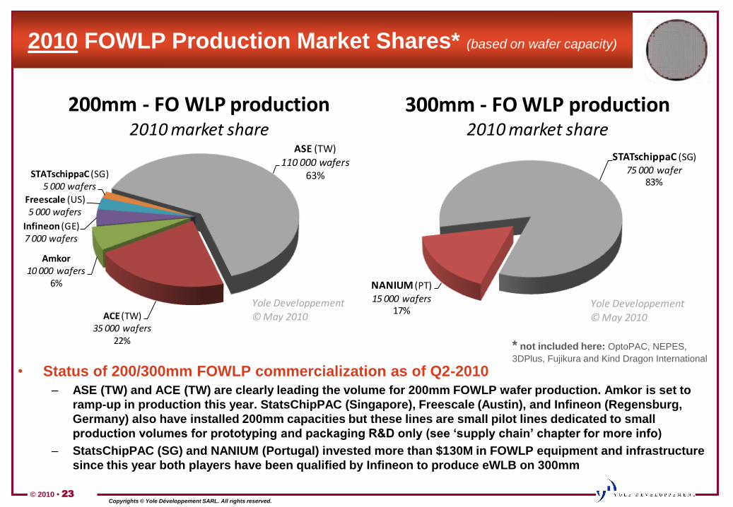
ASE (TW)110 000 wafers
63%
ACE (TW)35 000 wafers
22%
Amkor 10 000 wafers
6%
Infineon (GE)7 000 wafers
Freescale (US)5 000 wafers
STATschippaC (SG)5 000 wafers
200mm - FO WLP production 2010 market share
Yole Developpement
© May 2010
2010 FOWLP Production Market Shares* (based on wafer capacity)
• Status of 200/300mm FOWLP commercialization as of Q2-2010
– ASE (TW) and ACE (TW) are clearly leading the volume for 200mm FOWLP wafer production. Amkor is set to
ramp-up in production this year. StatsChipPAC (Singapore), Freescale (Austin), and Infineon (Regensburg,
Germany) also have installed 200mm capacities but these lines are small pilot lines dedicated to small
production volumes for prototyping and packaging R&D only (see „supply chain‟ chapter for more info)
– StatsChipPAC (SG) and NANIUM (Portugal) invested more than $130M in FOWLP equipment and infrastructure
since this year both players have been qualified by Infineon to produce eWLB on 300mm
* not included here: OptoPAC, NEPES,
3DPlus, Fujikura and Kind Dragon International
STATschippaC (SG)
75 000 wafer83%
NANIUM (PT)
15 000 wafers17%
300mm - FO WLP production 2010 market share
Yole Developpement © May 2010
© 2010 • 24Copyrights © Yole Développement SARL. All rights reserved.
FOCUS ON 3D TSV.
© 2010 • 25Copyrights © Yole Développement SARL. All rights reserved.
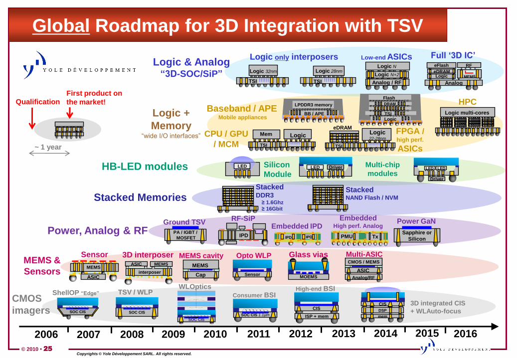
Global Roadmap for 3D Integration with TSV
2007 2008 2009 2010 2011 2012 2013 2014 20162006 2015
MEMS &
Sensors
MEMS cavity
MEMS
Cap
Sensor
ModuleMEMS
ASIC
CMOS
imagersSOC CIS
WLOptics
SOC CIS
ShellOP “Edge”
SOC CIS
TSV / WLP
SOC CIS 1.1µm
Consumer BSI
3D interposer
interposer
ASIC MEMS
Multi-ASICCMOS / MEMS
ASIC
Analog/RFSensor
Opto WLP
MOEMS
Glass vias
Power, Analog & RFIPD IPD
Embedded IPDPA / IGBT /
MOSFET
Ground TSV
Stacked DDR3
≥ 1.6Ghz
≥ 16Gbit
Stacked NAND Flash / NVMStacked Memories
Logic +
Memory “wide I/O interfaces” Mem Logic
TSI
CPU / GPU
/ MCM
eDRAMLogic22-28nm
TSI
FPGA / high perf.
ASICs
Logic & Analog “3D-SOC/SiP”
HB-LED modules LED Driver Multi-chip
modulesLED Silicon
Module
CIS
High-end BSI
ISP + mem
Low-end ASICsLogic N
Logic N+2
Analog / RF
PMU Tx
Embedded High perf. Analog
QualificationFirst product on
the market!
~ 1 year
Baseband / APEMobile appliances
RFeFlash
Logic
Analog
eDRAMMEMS
Full „3D IC‟
Logic multi-cores
HPC
RF-SiP
IPD
Logic 32nm
TSI
Logic only interposers
Logic 28nm
TSI
3D integrated CIS
+ WLAuto-focusDSP
mem
CIS
Logic
Flash
TSI
DRAM
BB / APE
LPDDR3 memory
Sapphire or
Silicon
Power GaN
LED
Driver
LED
© 2010 • 26Copyrights © Yole Développement SARL. All rights reserved.
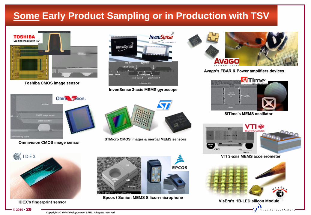
Some Early Product Sampling or in Production with TSV
Avago‟s FBAR & Power amplifiers devices
VTI 3-axis MEMS accelerometer
VisEra‟s HB-LED silicon ModuleIDEX‟s fingerprint sensor
Omnivision CMOS image sensor
Epcos / Sonion MEMS Silicon-microphone
Toshiba CMOS image sensor
InvenSense 3-axis MEMS gyroscope
STMicro CMOS imager & inertial MEMS sensors
SiTime‟s MEMS oscillator
© 2010 • 27Copyrights © Yole Développement SARL. All rights reserved.
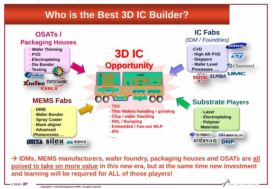
Who is the Best 3D IC Builder?
IDMs, MEMS manufacturers, wafer foundry, packaging houses and OSATs are all
poised to take on more value in this new era, but at the same time new investment
and learning will be required for ALL of those players!
3D IC Opportunity
MEMS Fabs- DRIE
- Wafer Bonder
- Spray Coater
- Mask aligner
- Advanced
Photoresists …
OSATs / Packaging Houses
- Wafer Thinning
- PVD
- Electroplating
- Die Bonder
- Testing
SRAM
SRAM
FLA
SH
Logic
Trans
ceiver
BAW / SAW filters Integrated PassivesDSP
PA module
SRAM
SRAM
DRAM
Control
ler
NOR
DRAM
DRAM
NAND
NAN
D
Substrate Players
- Laser
- Electroplating
- Polymer
Materials
- TSV
- Thin Wafers handling / grinding
- Chip / wafer Stacking
- RDL / Bumping
- Embedded / Fan-out WLP
- IPD
- …
IC Fabs(IDM / Foundries)
-CVD
- High AR PVD
- Steppers
- Wafer Level
Processes ….
© 2010 • 28Copyrights © Yole Développement SARL. All rights reserved.
FOCUS ON SILICON AND GLASS
INTERPOSER.
© 2010 • 29Copyrights © Yole Développement SARL. All rights reserved.
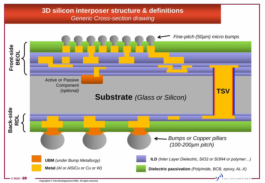
3D silicon interposer structure & definitionsGeneric Cross-section drawing
Substrate (Glass or Silicon)
Fro
nt-
sid
e
BE
OL
Fine-pitch (50µm) micro bumps
Bumps or Copper pillars
(100-200µm pitch)
Active or Passive
Component
(optional) TSV
Back
-sid
e
RD
L
UBM (under Bump Metallurgy)
Metal (Al or AlSiCu or Cu or W) Dielectric passivation (Polyimide, BCB, epoxy, AL-X)
ILD (Inter Layer Dielectric, SiO2 or Si3N4 or polymer…)
© 2010 • 30Copyrights © Yole Développement SARL. All rights reserved.
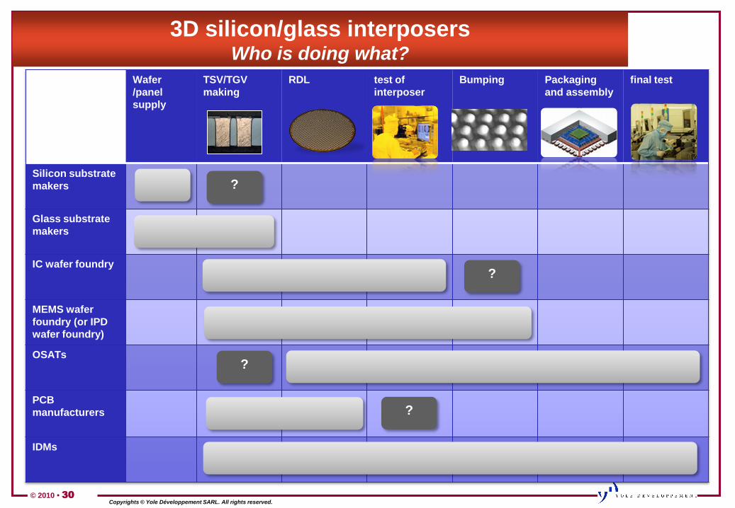
3D silicon/glass interposersWho is doing what?
Wafer
/panel
supply
TSV/TGV
making
RDL test of
interposer
Bumping Packaging
and assembly
final test
Silicon substrate
makers
Glass substrate
makers
IC wafer foundry
MEMS wafer
foundry (or IPD
wafer foundry)
OSATs
PCB
manufacturers
IDMs
?
?
?
?
© 2010 • 31Copyrights © Yole Développement SARL. All rights reserved.
Mid-end Packaging InfrastructureFirst conclusions
• „Mid-end‟ business ~ 20% of BE packager revenues by 2016
– Driver for these players is to sustain growth & preserve margins in this cost
competitive market
– Challenge: annual R&D investment budget usually low
• „Mid-end‟ business ~ 2% of FE semiconductor revenues by 2016 only
– Not driven by revenues generated!
– Rather interested by the potential behind this integration:
• In order to package everything by themselves and not rely on
subcontractors as packaging is now becoming increasingly strategic to
control!
• To climb in the electronic value chain by integrating more additional
functions and moving to “system” integration
• High interest for 3D from system integrator companies in medical (Medtronic,
SJM…) and automotive areas (Honda, Toyota, Denso, Bosch…)
– 3D IC integration with TSV implies possible changes in the electronic value
chain: could OEMs & system integrator players become the next “SOC
makers”?
© 2010 • 32Copyrights © Yole Développement SARL. All rights reserved.
For more information …
Take a look at our websites
www.i-micronews.fr
Please make a stop at Yole booth: N° C2135
Feel free to give me your business card to receive the electronic copy of my slides.