semiconductor switches for aerospace alternating- current power applications … · 2013-08-31 ·...
TRANSCRIPT

NASA TM X-1495
SEMICONDUCTOR SWITCHES FOR AEROSPACE ALTERNATING-
CURRENT POWER APPLICATIONS
By J a m e s Vrancik
Lewis Research Center Cleveland, Ohio
D
NATIONAL AERONAUTICS AND SPACE ADMINISTRATION
For sale by the Clearinghouse for Federal Scientific and Technicol Information Springfield, Virginia 22151 - CFSTl price $3.00
e .
https://ntrs.nasa.gov/search.jsp?R=19680006180 2018-07-13T17:23:36+00:00Z

SEMICONDUCTOR SWITCHES FOR AEROSPACE ALTERNATING-
CURRENT POWER APPLICATIONS
by James V r a n c i k
Lewis Research Center
SUMMARY
The purpose of this investigation was to obtain insight into the merits and drawbacks of ac static switches, with particular attention to their application as aerospace power switches.
Several ac static switches utilizing various semiconductor devices were studied with attention given to power loss, harmonic content, leakage, and temperature effects.
The main desirable characteristics are probable high reliability (based on the fact that there are no known wear out modes) and long life, no moving parts, high vibration and shock resistance, and immunity to atmospheric conditions.
A specific design was made to provide an example application for the devices and circuits investigated in this report. A breadboard-type three-phase static switch for space use was designed, built, and tested. The breadboard switch was used as a motor starter for a 4-ampere fuel pump motor. The switch performance was determined and the power loss found to be 12 watts while transferring 800 watts (1.4 kVA). Other char- acteristics determined were harmonic content (( 1.0 percent) and leakage (resistance in off state 2 50 kQ). The switch was tested over a heat-sink temperature range of -40' to 80' C.
INTRODUCTION
Switches intended for operation in aerospace power systems must generally meet such requirements as long life, high reliability, operation in a vacuum as well as full and partial atmospheres, etc. These requirements are not readily achieved with electromechanical switches. Since semiconductors, such as transistors and silicon con- trolled rectifiers (SCR's), are now considered quite reliable, capable of long life, and

contain no moving parts, there has been considerable effort expended to utilize these ?'static" elements to replace electromechanical devices such as switches and relays (see refs. 1 to 3).
Static switches are well suited for applications such as feedback control, positioning of antennas or solar arrays, or other applications that require a large number of oper- ations since their reliability does not appear to be a function of the number of operations.
The purpose of this investigation was to obtain insight into the merits and drawbacks of static ac switches with particular attention to their application as aerospace ac power switches.
the merits of transistors, silicon controlled rectifiers (SCR's), and bidirectional triode thyristors when used for alternating-current switching. Particular interest was paid to the power loss in the switch as a function of load current, and the effect of tempera- ture on the performance of the switch. Other characteristics such as rroff'' losses and harmonic content were also considered.
This discussion is limited to the power handling components of an ac static switch. The triggering of a switch, although important, is too large a subject to be discussed herein. Usually, the means of triggering a switch are determined by the specific appli- cation and the type of power supplies available.
The characteristics of SCR's, transistors, and bidirectional triode thyristors were compared to determine the most appropriate load-carrying semiconductors for use in a static switch for motor control.
A specific design was made to provide an example application for the devices and circuits investigated. A breadboard model of a switch which will operate a 400-hertz three-phase 120/208 -volt, 4-ampere pump motor was designed, built, and tested. One of the most significant characteristics of the breadboard switch is that the power needed to turn on the load-carrying elements is drawn from the voltage drop across the switch, instead of being supplied by the control signal.
An important area of future study in the field of static switches which is not dis- cussed in this report is reliability. Semiconductors supposedly have a relatively high reliability, but a static switch uses a number of semiconductors along with passive ele- ments, such as resistors and capacitors, so it is important to determine the reliability of the complete assembly.
In this investigation, several single-phase static switches were studied to determine
1
'A bidirectional triode thyristor is a device which may be triggered from blocking to conducting state for either polarity of applied voltage. This device will perform most of the functions of two SCR's connected in inverse parallel.
2

IN IT I AL INVEST I G AT IO N
Three basic a c switching arrangements that can be employed in static switches are shown in figure 1.
The symbol [ T I is for control elements such as transistors, SCR's or bidirec- tional triode thyristors. The arrow indicates current direction.
The circuit of figure l(a) contains only two devices, or one in each current path, so it represents the minimum power loss possible for a static switch.
When in the off or blocking state, both devices are subjected to full line voltage in both the forward and reverse directions. When in the on or conducting state, each de- vice is subjected to a reverse voltage equal to the forward conducting voltage of the other device.
The circuit of figure l(b) contains four devices and therefore has more power loss. However, it has the advantage of having a common control point which may simplify the control circuit.
Neither control device is ever subjected to a reverse voltage greater than the for- ward conducting voltage of the parallel diode (= 1 V). However, when in the off state, the diodes are subjected to a reverse voltage equal to full line voltage, and the parallel control devices are subjected to this same voltage, but in their forward direction. Thus, the control devices must be capable of blocking full line voltage in the forward direction and 1 volt in the reverse direction.
The circuit of figure l(c) contains five devices (three in each current path) and therefore has the highest power loss. It has the advantage of only one control element and therefore needs only one control signal. This control element is active in both cur- rent directions, so it carr ies twice the average current (and dissipates twice the power) as each control element in the other circuits.
The control device is never subjected to a reverse voltage but, of course, it must be capable of withstanding full line voltage in the forward direction. If the control de- vice for this switch is a SCR, difficulty may be encountered at high supply frequencies in turning the switch off due to an insufficient amount of time for the device to commutate.
(a) Inverse-parallel. (b) Back to back. (c) Bridge.
Figure 1. - Alternating-current static switching arrangements.
3

The basic switching arrangements of figure 1 can be used with SCR's and transis- tors. However, the state-of-the-art of transistors greatly limits the voltage of the sys- tem when the switch is built in arrangement (a) since the base-to-emitter junction must be able to withstand full line voltage when the switch is in the off state. For typical high power silicon transistors, the base-to-emitter breakdown voltage is 15 to 20 volts maxi- mum, which is unsuitable for all systems with voltages higher than 15 volts rms . How- ever, transistors are readily available for use in switch configurations (b) and (c).
A third type of semiconductor that can be used in a static switch is a bidirectional triode thyristor. A bidirectional triode thyristor is a four-layer silicon device that has the electrical characteristics of two inverse-parallel SCR's; that is, the device can be triggered from a blocking state to a conducting state for either polarity of applied volt- age. The triggering signal required is of the same magnitude as that needed for a SCR, but unlike the SCR, the signal can be of either polarity. Since it is a single device, it requires only one heat sink, whereas two are needed for the inverse-parallel SCR switch.
Power Loss as Function of Current
To compare the different switch configurations using different semiconductor de- vices, the power loss (as a function of current) of each device is calculated. Then, to find the power loss of a given configuration, all that is necessary is to add the power losses of the series components.
sine wave: It can usually be assumed that the current through the device is a half-wave rectified
1 = 1 s i n 8 O s 6 < a M
I = 0 a 5 8 < 2 a
The average power loss in a semiconductor device can be calculated by using
2a p l o s s = ~ ~ Ivde
The voltage drop for a diode, SCR, or a bidirectional thyristor can be approximated by equation (3) and for a transistor by equation (4):
4

V = A + B log I
V = IRsat
(3)
(4)
where
V
I instantaneous cur rent
peak current
instantaneous vo It age drop
IM A, B constants
Rsat saturation resistance of transistor
Equation (3) is not the usual form found in textbooks o r specification sheets. However, an examination of any specification sheet for SCR's, diodes, or bidirectional triode thyristors will show that when the logarithm of the forward current is plotted against the voltage drop, the curve is essentially linear within the rating of the device. Equation (3) expresses this linear dependence. The power loss is then
when combining (1) , (2), and (3) and integrating, or
- - IkRsa t 'loss 4
when combining (1), (2), and (4) and integrating. The relative power loss of the various semiconductors can be compared by selecting the current state-of-the-art components and applying the corresponding power loss calculation.
For comparison, semiconductors rated to operate in a switch configuration with a sine wave of current of 10 amperes peak and a voltage of 400 volts peak were considered. With these devices and adequate cooling, the switch would have a nominal rating of 5 ampere rms and 220 volts rms.
perature of 25' C was found to be The SCR selected was a MCR1308. The maximum voltage drop at a junction tem-
V = 1.19 + 0.15 log I
from reference 4.
5

The diode chosen was a 1N1206A suitable for spacecraft application (JPL JPEC ZPP 2746-3006-€3). The maximum voltage drop was found to be
V = 0.883 + 0 .12 log I
from reference 5.
0 . 1 ohm (see ref. 6) or The transistor selected was a 2N2583 and had a maximum saturation resistance of
v = I(0. 1)
The bidirectional triode thyristor chosen was a SC45D. The maximum voltage drop was found to be
V = 1.06 + 0 . 3 9 log I
from reference 7.
rent as a function of peak current. The power loss of the SCR, diode, and bidirectional triode thyristor are approximately straight lines since the forward voltage across these devices is nearly constant for all values of current within their ratings. Therefore, the power loss is approximately proportional to the current. The transistor, however, re- sembles a constant resistance so i ts power loss is proportional to the current squared.
The various static switch configurations can now be compared by adding the power loss of the components. As an example, referring to figure 1, the power loss of cir-
Figure 2 shows the power loss of the various semiconductors for one half-wave cur-
Figure 2. - Power loss of various semiconductors when conducting one-half sine wave of current.
6

TABLE I. - COMPARISON O F POWER LOSS
O F VARIOUS SWITCH CONFIGURATIONS
I Power loss
General equation Value for IM= 7A
W @RMs = 5 ~ ) 7
5.4
9.4
13.4
6.4
5.4
5.0
cuit (a) is the sum of the losses of two SCR's, each conducting one-half of a sine wave of current (2PScR(IM)).
rms. The switches can be grouped into two groups according to their power loss. Switches A, D, and F have losses between 5 and 6 .5 watts. The inverse-parallel SCR switch (A) and its electrical equivalent, the bidirectional triode thyristor (F), have the lowest power loss. The thyristor has the added advantages of being packaged in one unit (one heat sink required) and having only one contact lead.
sistor bridge circuits (C and E) understandably have the highest power loss (3 compo- nents in series in each leg).
Table I compares the power loss of the various circuits when conducting 5 amperes
Switches B, C, and E have losses between 9.4 and 13.4 watts. The SCR and tran-
When comparing B to D and C to E, it can be seen that when a transistor replaces a
7

SCR, the power loss of the switch decreases. This is due to the fact that for devices which have the same maximum current rating the power loss of the transistor is signifi- cantly less than that of a SCR.
When low power loss is a main objective, the obvious circuits to use are A, I) and F in table I.
Off Los se s
Since transistors and SCR's do not exhibit infinite resistance characteristics in the off state, the small but finite current that does flow can cause heating that can damage the semiconductor. Typical high quality SCR's, such as the MCR 1308, used to illus- trate "on" losses have a minimum effective blocking resistance of 50 kilohms. In a 120-volt system, this represnets an off loss of 300 milliwatts.
A diode, such as the previously mentioned 1N1206A, has a minimum resistance of 600 kilohms. In a 120-volt system, this represents an off loss of only 25 milliwatts.
A transistor, such as the 2N2580, has a minimum blocking resistance of 100 kil- ohms, which represents a loss of 150 milliwatts in a 120-volt system. And last, the bidirectional triode thyristor has a minimum blocking resistance of 80 kilohms, which represents a loss of 180 milliwatts in a 120-volt system.
These numbers are for specific devices, but they represent approximately the state-of -the-art of semiconductors. In general, SCR's usually have the lowest blocking resistance and diodes, the highest, with transistors and bidirectional triode thyristors somewhere in between.
HARMONIC CONTENT
Due to the nonlinear voltage drop across the switches, harmonics are introduced into the load voltage, which, for some applications, may be undesirable. An examina- tion of some of the characteristics of semiconductors can show how some of the harmonic content is produced.
An SCR, or a diode, can be represented by a high resistance until the current through it is high enough to take it past the knee of the current-voltage curve where it then takes on the characteristics of a constant voltage drop. This effect tends to distort the leading part of the sinusoid of voltage across a load in series with the SCR or diode.
of the SCR into conduction. If 0 is the angle in degrees that conduction is delayed (see fig. 3) then the total harmonic content (THC) introduced into the sine wave is THC (percent) 5 0 . 4 0: (see appendix A).
This effect can be made more pronounced with a SCR circuit by delaying the firing
8

Figure 3. - Sine wave with conduction delayed by Boo.
ultant wave, ?Es + E' sin wt
rE' sin wt I
Figure 4. - Square wave plus a s ine wave used to approximate the voltage drop across a n ac static switch.
Since
then
eo = 0.44 t
in a 400-hertz system and
THC 5 0.06 t percent
i f t is in microseconds. Thus, if a static switch takes 20 microseconds to turn on, the THC introduced by this delay would be less than 1 .2 percent.
square wave, the total harmonic content in the resultant voltage wave of the load (sine minus square) is
If the voltage drop across a static switch during conduction is approximated by a
THC (percent) = (9)
(see appendix B) where Es is the voltage of the square wave across the switch and Eo is the peak voltage of the supply sine wave. Finally, if the voltage drop across a switch
9

is approximated by a square wave plus a sine wave, and the sine wave has a maximum voltage of E (see fig. 4), then the harmonic content is 1
( 4 / 4 Es( 100) THC (percent) =
Eo - (4/r)ES - E'
For example, if a 5-ampere transistor switch voltage drop can be approximated by a square wave of 0 . 6 volt plus a sine wave of 0 . 6 volt when the peak line voltage is 160 volts, then
Es = 0 . 6 V
1 E = 0 . 6 V
Eo = 160 V
THC = 0 . 3 percent
The specific application will determine if this amount of total harmonic distortion is ac- ceptable or not.
troduced on the a c load by the switch, which may be caused by unequal voltage drops across the switch during opposite halves of the sine wave. However, this is usually less than 0 .1 volt, and with proper component selection, it can be reduced even further.
Another form of distortion that can be caused by a static switch is a de voltage in-
TEMPERATURE EFFECTS
As the temperature of an SCR is increased, the forward voltage drop, at currents within its rating, decreases slightly and the losses in the SCR decrease (see refs. 4 and 5).
For the SCR MCR 1308 previously discussed, the voltage drop decreases to V = 1.08 + 0.183 log I when the junction temperature is increased from 25' to 100' C. This corresponds to a change in power'loss of from 2.70 to 2.46 watts or 9 percent at a peak current of 7 amperes. This same effect is present in diodes and bidirectional triode thyristors, but in transistors the effect may be in either direction, depending on type (PNP or NPN), material, doping, etc. It has already been pointed out that the power loss in the switch, when it is in the off state, can be significant compared to its
10

loss when conducting. This is especially true when the switch is at a high temperature since the leakage of the components in the reverse direction increases as temperature increases. This increased leakage current tends to heat the junction even more, pro- ducing more leakage. Eventually, thermal runaway may occur unless proper cooling techniques are used. The junction temperature limits of state-of -the-art silicon semi- conductor is from -65' to 125' C with some SCR's and transistors rated as high as 150' C and some diodes rated as high as 200' C.
OVERLOADS AND OVERVOLTAGE
In the event of a fault in the load circuit, the semiconductors can be damaged if not properly protected. The most common method of protection is to fuse the switch con-
2 sistent with the I t rating and surge ratings of the semiconductors used. Some loads will draw high inrush or surge currents at startup, and both the fuse and
the semiconductors must be capable of withstanding this current. The ability of a semi- conductor to withstand this current is given in the ratings as the maximum nonrecurrent peak surge forward current.
The switch must be protected against voltage transients in the line voltage or the load exceeding the breakdown voltage of the semiconductor used in the switch. This can be done by using a line filter or a semiconductor that has a higher breakdown voltage than any transient voltage that may occur. In general, semiconductors are available with breakdown voltages in excess of 600 volts.
DESIGN OF BREADBOARD SWITCH FOR SPECIFIC APPLfCATlON
Requi rements
A static switch was designed for the specific application of motor starting. For this investigation a three-phase, 120/208-volt, 4OO-hertz, 4-ampere, motor (see fig. 5) was used to power an aircraft booster fuel pump.
It was assumed that a 10-volt dc signal would be available to turn the switch on, and removal of this voltage would turn the switch off. It was further assumed that no other power supply would be required to operate the switch. An attempt was made to mini- mize the losses of the switch and the control power required to operate it. The switch was to operate with a heat-sink range of -40' to 80' C.
were experimentally determined. The startup characteristics of the motor are shown in For the purpose of describing the load, some of the characteristics of the motor

C-66-3966
Figure 5. - Fuel pump and motor assembly.
Time, sec
Figure 6. - Motor startup and turnoff.
figure 6 where the top trace is the line-to-line voltage at the load with a steady-state value of 3.75 amperes rms. A peak current of 9.75 amperes rms or 2.6 per unit was drawn at startup from the power supply used. Since the power supply voltage drooped during startup, a higher current would be expected from a stiffer power supply.
in figure 7.
shown in figure 8.
The phase relation between voltage and current for steady-state operation is shown
Curves of line-to-line voltage and power factor as a function of line current are
12

> ai m rn
0 > c -
360
180
0
-180
-360
a c- S 0 L L
3 U
I In1 I I I I I I I I
3.50 3.70 3.90 4.10 4.30 4.50 4.70 Line current, A-rrns
Figure 8. - Motor characteristics.
0 .58
13

D esc r i pt io n of Switch Opera t i o n
The decision to use SCR's instead of bidirectional triode thyristor or transistor was achieved by the process of elimination. Bidirectional triode thyristors are not yet avail- able in the current range required to operate the pump motor with sufficient safety mar- gin.
an inductive load such as the pump motor (power factor of 0.60), a large inductive volt- age spike may occur and damage the transistor. Thus, special circuits must be used to either protect the transistor from these spikes or to increase the time for the transistor to turn off.
have the characteristic of turning off only when a zero current condition exists, thus eliminating all voltage spikes.
The design philosophy called for a minimum amount of power drain from the control signal. It was therefore decided that the control signal would be used to turn on a small switch which, in turn, would supply turnon power to the main SCR's from the ac line.
Since the control signal may or may not be grounded, it was decided to use an oscillator-transformer-rectifier circuit to provide isolation between the control signal and the switch. This also allows the use of only one control signal to operate all three phases of the switch.
oscillator circuit, rectifier and filter, drive circuit, and power-handling circuit.
alternately conduct and cut off. This circuit is commonly called a Royer Oscillator (see ref. 8). The oscillator was originally designed for operation at 1 kilohertz, but due to high losses in the transformer, the frequency was lowered to 300 hertz.
The input is 10 volts dc at 10 milliamperes (100 mw) and the oscillator efficiency is approximately 60 percent, leaving an output power of 60 milliwatts. It was experi- mentally determined that the switch would operate over its temperature range with con- trol signal input of 5 volts at 5 milliamperes. Below this voltage the oscillator (and thus the entire switch) would be inoperative.
6 milliamperes each. Each winding feeds a full-wave bridge rectifier and filter, the output of which is 2 volts. This voltage is applied to the drive transistor (Q3) which sat- urates and in turn supplies power from the power line to the power handling SCR's
Transistors, however, will turn off as soon as the base drive is removed, and for
However, SCR's are readily available in the current ranges being considered and
The four main sections (see fig. 9) of the switch design for this application a r e
The oscillator is an astable multivibrator which utilizes two signal transistors that
The oscillator transformer has three output windings, designed for 3.5 volts at
through D5, D8, R7 and D6, D7, R6. .
14

Load
Oscillator c i rcu i t Transformer, rectif ier and f i l ter Drive c i rcu i t Power-handling c i rcu i t
Figure 9. - Alternating-current static switch c i rcu i t diagram,
The switch has positive turnon for any temperature between -40' to 80' C when the power line voltage is greater than or equal to 8 volts.
Under normal conditions, the drive transistor dissipates less than 0 . 1 watt. How- ever, if the switch is turned on when the ac supply voltage is at its maximum, the base drive will not be sufficient to hold the transistor in saturation. For this particular ap- plication, it was found that as much as 225 watts peak power may be dissipated in the drive transistor; thus, a high power transistor must be used.
of 14 amperes for a range of heat-sink temperatures from -40' to 80' C. The switch has a design rating of 4 amperes and has a continuous overload capability
APPARATUS AND TEST PROCEDURE
Since the apparatus and test procedure are of secondary importance to this report, they were placed in appendix C.
15

TEST DATA AND RESULTS
Power Loss
The power loss in the switch was measured as a function of the line current for vari- ous heat-sink temperatures. The experimental data are presented in figure 10, and photographs of the voltage drop across the switch at various temperatures are shown in figure 11. The curves and photographs show that the power loss per unit current de- creases as temperature increases. The curves are approximately straight lines since the voltage drop across a SCR does not vary appreciably as the current changes.
one half-wave of current is It was shown at the beginning of this report that the power loss of an SCR conducting
- ! e ( . + l o g 2 - l + l 0 g I N I ) - ploss
Since the switch has s ix SCR's, the total power loss is
ploss, total = 6ploss
temperature,
16
15
?Z 14 VI- VI 0 - L
13 a
12
11 3.5 3.7 3.9 4.1 4.3 4.5 4.7
Line current, A-rms
Figure 10. -Total power loss in three-phase ac static switch as function of line current.
16

0 1 2 3 4 5
(a) Current, 3.9 amperes; heat-sink temperature, 80' C.
0 1 2 3 4 5
(bbcurrent , 3.9 amperes; heat-sink temperature, 30" C.
0 1 2 3 4 5
Time, msec
(c) Current, 3.9 amperes; heat-sink temperature, -40' C.
Figure 11. - Switch voltage as a function of t ime and temperature.
17

The constants were determined to be
A = 1.21
B = 0.22
from reference 9. The curve of calculated power loss is superimposed in figure 10. A total of 1365 volt-amperes and 830 watts was delivered to the motor at 210 volts
line-to-line and 3.75 amperes. At this current, the switch loss was 12 watts at 46' C. This results in an efficiency of
830 830 + 12
x 100 = 98.6 percent
It should be realized that such efficiency figures may be misleading since the loss in the switch is determined almost completely by the current passing through it. In a high voltage system, a given switch would have a higher efficiency than it would in a low voltage system for the same power transfer.
The drive circuit used for this switch draws no more than 2 milliwatts average power from the power line, so there would be little to gain by improving its efficiency.
Off Losses
the The leakage of the switch when in the off condition was measured
ambient temperature at rated voltage (see fig. 12).
120
100
5 80
YI
E,
c' [I: a I I
60 :e m m Y m
3 40
20 0 20 40 60 80 100 120
Heat-sink temperature, "C
Figure 12. - Switch leakage (120-V system) a s function of temperature.
as a function of
18

Time, msec
Figure 13. - Leakage current through three-phase static switch at 80" C heat- sink temperature.
At a heat-sink temperature of 80' C, the switch has a leakage current of 55 micro- amperes at a line-to-neutral voltage of 120 volts rms. This corresponds to an effec- tive resistance of greater than 2 megohms. At room temperature, the effective resist- ance is 5 megohms.
figure 13. The off power loss in the switch at 80' C is approximately 6 milliwatts due to leakage; therefore, a small amount of cooling must be provided to keep the semi- conductor temperature below the rated maximum.
A photograph of the 400-cycle leakage current waveshape at 80' C is shown in
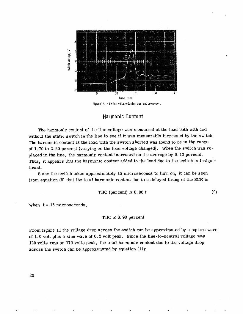
Commutation Time
The minimum commutation time for this application will be defined as the amount of time the sine wave takes to go from -1 to 1 volt (the drop across an SCR during conduc- tion). In a 129-volr: 400-hertz system, this time is 4 .7 microseconds. The total com- mutation time measured from figure 14 is approximately 15 microseconds. During the commutation time, a voltage r i se occurs across the switch. This voltage rise is due to the fact that a voltage (no greater than 8 V) must be present across the firing circuit to provide power to the gates of the SCR's to turn them on. The fact that this voltage rise must be present to turn the SCR's on partially explains the increase in commutation time from 4.7 to 15 microseconds. This voltage rise could be eliminated by supplying SCR gate power directly from the control signal at the expense of increased size and weight of the control signal circuit.
19
>
Time, p e c
Figure 14. - Switch voltage dur ing cur ren t crossover
Harmonic Content
The harmonic content of the line voltage was measured at the load both with and without the static switch in the line to see if it was measurably increased by the switch. The harmonic content at the load with the switch shorted was found to be in the range of 1.70 to 2.50 percent (varying as the load voltage changed). When the switch was re- placed in the line, the harmonic content increased on the average by 0.13 percent. Thus, it appears that the harmonic content added to the load due to the switch is insigni- ficant.
Since the switch takes approximately 15 microseconds to turn on, it can be seen from equation (9) that the total harmonic content due to a delayed firing of the SCR is
THC (percent) i 0.06 t (9)
When t = 15 microseconds,
THC i 0.90 percent
From figure 11 the voltage drop across the switch can be approximated by a square wave of 1.0 volt plus a sine wave of 0.2 volt peak. Since the line-to-neutral voltage was 120 volts r m s or 170 volts peak, the total harmonic content due to the voltage drop across the switch can be approximated by equation (11):
20

4/aEs( 100) THC (percent) =
Eo - 4/nEs - E'
where
E, = 1.0 V
Eo = 170 V
E' = 0.2 V
THC = 0.37 percent
Thus, for the worst case, the THC due to the switch cannot exceed 0.9 + 0.4 percent or 1.3 percent. Experiment shows the THC of the load increases 0.13 percent on the av- erage due to the static switch.
Characteristics During Turnon and Turnoff
The turnon time is defined as the time between the application of the control signal
Figure 15 illustrates the turnon of the static switch. The control signal was applied and full conduction of the switch.
at the point where the sweeps begin (the oscilloscope was triggered by the control sig-
4
300 -- E L L > 3
- c 8
S
$ 150 > 0 3
g o 3 VI
-1%
0 .4 .8 1.2 1.6
Time, msec
Figure 15. - Turnon characteristics of three-phase static switch control signal applied at t ime zero. 21

Q
c- S a L L
3 u a S -I .-
> 3MJ
0 0
-300
a- m m
> U m 0
c -
Time, msec
Figure 16. - Turnoff characteristics of three-pane static switch control signal removed at time zero.
nal). The top curve shows the current through the switch, and the lower curve shows the voltage across the switch. The voltage collapses to zero (*l V) and the current begins approximately 200 microseconds (sweep speed of 200 psec/cm) after the control signal was applied. If the filter capacitor C3 of figure 9 was made smaller, the turnon time would decrease at the expense of more ripple being sent to the base of the drive transistor. The choice of a 0.1-microfarad capacitor was a compromise between low ripple and high speed.
The turnoff time will not be defined since the only way an SCR can be turned off is by reducing the current to zero. Therefore, with no control signal, the gate drive is removed from the SCR's and the switch will turn off the next time the sine wave of cur- rent passes through zero. Figure 16 illustrates the turnoff of the switch. The top curve is the current through the switch and the bottom curve is the voltage across the load. A s the current tries to reverse, the switch turns off and the voltage across the load drops to the induced voltage of the motor (generator action).
Figure 16 seems to indicate that the current overshoots and then slowly lreturns to the zero position, but this is actually due to the discharge of a capacitor at the input of the oscilloscope.
Design Improvement
A small but significant design change was made at the end of the test program. As was pointed out earlier, it is possible for the drive transistor (Q3) (see fig. 9) to dissi- pate over 200 watts for a short time if the switch is turned on at the peak line-to-line voltage. This necessitates using a large power transistor €or the drive transistor. A
22
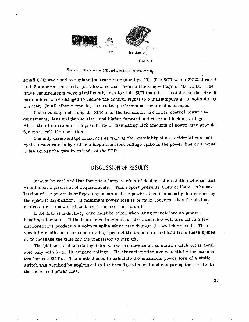
SCR Transistor Qg
C-66-3970
Figure 17. - Comparison of SCR used to replace drive transistor Q9
small SCR was used to replace the transistor (see fig. 17). The SCR was a 2N2329 rated at 1.6 amperes r m s and a peak forward and reverse blocking voltage of 400 volts. The drive requirements were significantly less for this SCR than the transistor so the circuit parameters were changed to reduce the control signal to 5 milliampers at 10 volts direct current. In all other respects, the switch performance remained unchanged.
The advantages of using the SCR over the transistor are lower control power re- quirements, less weight and size, and higher forward and reverse blocking voltage. Also, the elimination of the possibility of dissipating high amounts of power may provide for more reliable operation.
cycle turnon caused by either a large transient voltage spike in the power line or a noise pulse across the gate to cathode of the SCR.
The only disadvantage found at this time is the possibility of an accidental one-half
DISCUSSION OF RESULTS
It must be realized that there is a large variety of designs of ac static switches that would meet a given set of requirements. This report presents a few of them. The se- lection of the power-handling components and the power circuit is usually determined by the specific application. If minimum power loss is of main concern, then the obvious choices for the power circuit can be made from table I.
handling elements. If the base drive is removed, the transistor will turn off in a few microseconds producing a voltage spike which may damage the switch or load. Thus, special circuits must be used to either protect the transistor and load from these spikes or to increase the time for the transistor to turn off.
The bidirectional triode thyristor shows promise as an ac static switch but is avail- able only with 6- or 10-ampere ratings. Its characteristics are essentially the same as two inverse SCR's. The method used to calculate the maximum power loss of a static switch was verified by applying it to the breadboard model and comparing the results to the measured power loss.
If the load is inductive, care must be taken when using transistors as power-
23
D

The calculation for the maximum total harmonic content predicted a maximum ap- proximately 10 times larger than that measured for the breadboard switch. However, the total harmonic content produced by the power supply was two times as large as the calculated maximum total harmonic content produced by the switch. It is difficult to predict how these two sources of harmonics combine. The harmonics produced by the switch may cancel some of the harmonics produced by the power supply making any measurement of the increase of total harmonic content almost meaningless.
400 hertz, 120/208-volt three-phase system used to control a 4-ampere motor. The switch can operate with a heat-sink temperature of from -40' to 80' C. The control of the switch is accomplished by supplying a low-power dc signal of 10 volts to the control terminals. A control current of 5 milliamperes was realized when an SCR was used in- stead of the drive transistor Q3. The transistor Q3 used a control current of 10 milliamperes.
The use of 400-hertz power supplies throughout this report should in no way imply a limitation to the frequency that an ac static switch can handle. However, 400 hertz was used for this report since it seems to be the most popular choice for space power systems presently under study. For higher frequencies, the harmonic content may in- crease slightly, but all other switch characteristics should remain the same (i. e., power loss, off loss, etc.).
The merits of the static switch must be weighed against this power loss for a given ap- plication.
It was found that the off losses were of the order of a few 10's of milliwatts. This power would usually be ignored except for the small amount of heating it would cause in the semiconductor.
The harmonic content introduced into the load was not precisely determined, but it does introduce less than 1 percent. This amount of harmonic content is negligible for the application of motor starting, but may be a consideration for other applications.
The turnon time was determined to be approximately 200 microseconds and turnoff occurred within one cycle of current after the removal of the control signal.
The power loss, harmonic content, off loss, and limited temperature range are all factors to be considered for any proposed application. The desirable characteristics of static switch are absent of moving parts (and the associated wear), and the high gain possibilities between the control power and the power transferred. Also, semiconduc- tors appear to have high vibration and shock tolerance, probable high reliability, and long life. In addition, semiconductors can operate in almost any type of atmosphere, and they are capable of a large number of operations.
The final switch in this investigation meets the requirements of operating in a
The 4-ampere ac switch tested had a total power loss of approximately 12 watts.
24

Due to their capacity for a large number of operation, static switches are particu- larly suited to applications such as on-off type regulation, position controls for the ori- entation of solar panels, radio antennas, flashing lights, etc. They are also useful in applications which require fast response time, such as the interconnection of alternators for parallel operation. Also, due to their relatively high resistance to shock and vibra- tion, a static switch is well suited to application where accidental switching caused by mechanical vibration or shock cannot be tolerated. For instance, a switch which acti- vates a rocket destruct mechanism or a door opening mechanism.
Lewis Research Center, National Aeronautics and Space Administration,
Cleveland, Ohio, September 8, 1967, 120 - 27 - 04 -43 - 2 2.
25
APPENDIX A
DETERMINATION OF TOTAL HARMONIC CONTENT
DUE TO FINITE FIRING ANGLE
For a sine wave with the first 9, degrees cut off, it can be shown that the Fourier series is
1 2
E = - a, + a1 cos e + a2 cos 28 + . . an cos ne + . . .
+ bl sin 0 + b2 s in 28 + . . . bn sin ne + . . .
where
a = O 0
'M 2 al = - -sin B o a
an = 0 for n = even
cos(1 - n)eo cos(1 + n)eo for n > 1 and odd I +
1 - n l + n
+ s i n e cos0 0
b = O for n = even n
IM bn = - a
26
- sin(1 - n)Oo _____ for n > 1 and odd
1 - n
sin(1 + n)Qo
- l + n I

and eo is the delayed conduction angle as shown in figure 3 (p. 9). When the Fourier series is used to determine the rms value of the fundamental and integration is per- formed under the curve to find the total r m s value of the wave, the total harmonic content can be determined by using
The relation between the total harmonic content and the firing angle is shown in figure 18. The straight line THC = 0.4 8, can be used to approximate the relation between
total harmonic content and firing angle for angles less than 20'.
25
2 20 2
E 15
W
W Q
e-
c C 0 u u I= .- 0 10 E
g 5
m xz - B
0 10 20 30 40 50 Firing angle, 8, deg
Figure 18. -Total harmonic content a s function of firing angle.
27

APPENDIX B
TOTAL HARMONIC CONTENT DUE TO VOLTAGE DROP ACROSS SWITCH
APPROXIMATED BY A SUMMATION OF SINE AND SQUARE WAVES
The voltage drop across an ac static switch can be approximated by the sum of a square wave and a sine wave.
The voltage across the load is the supply voltage minus the switch drop. Knowing this, one can calculate the total harmonic content (THC) of the load voltage assuming a perfect sinusoid of voltage from the supply.
28

Ein = Eo s in 6
3 - - ~ ~ i n 0 +------- s in 30 +- sin 50 + . . Esq a 3 5
Esin = E' s in 0
- - - n= 3 odd
4 E, X 100 a THC (percent) =
4 Eo - E' - - Es a
29

APPENDIX C
Instrument type
Iron vane (0 to 250 V) I ron vane (0 to 10 A ) Electrodynamometer
True rms, electronic
Electronic meter Electrodymamometer
(0 to 20 W) Mu1 t ipoint, potent iometei
(0 to 500 W)
meter
APPARATUS AND TEST PROCEDURE
Accuracy
22-Percent F. S.a +?Percent F. S. a +1/4-Percent F. S. a
&!-Percent reading
23-Percent readin kU4-Percent F. S. 2
The switch was used to control an aircraft booster fuel pump mounted in a 55-gallon drum of kerosene. The source of power was a 2.5 kVA, 120/208-volt, three-phase, 400- hertz aircraft rotating inverter power supply.
The line-to-line voltage, line current, control current and voltage, and the load power in each phase were constantly monitored (see fig. 19).
The power loss in each phase of the switch was measured with a high precision watt- meter for various currents and temperatures.
Oscilloscope pictures were taken of the voltage drop across the switch, and the com- mutation (zero) time of the switch was measured from these pictures. A distortion an- alyzer was used to measure the harmonic content across each phase of the load with, and without, the switch in the line.
The leakage through the switch in the off condition and the power loss in the switch in the on condition were recorded as a function of heat-sink temperature.
Oscilloscope pictures were taken of (1) the voltage drop across the switch, (2) the current through the switch, and (3) the voltage drop across the load during turnon and
Power supply
400 Hz, three
grounded)
N
15-MHz oscillo- - scope P,
To measure
Line-to-line voltage, VLL Line current, IL Load power,
Line-to-neutral voltage, VLN
Harmonic content, HC Switch power, P,
Temperature
a ~ . s., full scale.
Figure 19. - Alternating-current static switch test circuit.
30

(a) Front.
C-66-3969 (b) Rear.
Figure 20. - Three-phase alternating-current static switch.
turnoff. A l l six SCR's and the three power transistors were mounted on one 6 by 6 by 3/16 inch aluminum plate and were electrically insulated from the plate by mica washers. The temperature at the following points were measured and recorded by means of a multipoint thermocouple recorder:
31

Figure 21. - Instrumentation for three-phase alternating-current static switch.
32

Kerosene (55-gal drum)
Figure 22. - Schematic of pump motor test setup.
(1) SCR stud (6) (2) Aluminum plate close to the SCR mounting nut (6) (3) Power transistor case (3) (4) Oscillator transformer (1)
A photograph of the actual switch is shown in figure 20, and the instrumentation is shown in figure 21. A schematic of the pump motor test setup is shown in figure 22.
The test schedule was as follows: (1) Measure the harmonic content in the load voltage with the switch shorted, for
(2) Measure the following at heat sink temperatures of -40' C, 40' C, and 80' C four different motor currents.
(a) Three-phase line currents (b) Three-phase line-to-line voltage (c) Voltage drop across switch (take pictures) (d) Total three-phase switch power (e) Total three-phase load power (f) Control voltage (g) Control current (h) Harmonic content of load voltage (i) All monitored temperatures
(3) Repeat test (1) to determine repeatability and stability of system. (4) Determine the turnon and turnoff characteristics of static switch. T) Measure leakage for heat-sink temperatures of -40' to 80' C.
33

REFERENCES
1. Marion, B. A. ; and Lenhart, N. D. : System Control and Protection for Paralleled Static Converters or Inverters. Rep. No. WAED64.44E (NASA CR-54242), Westinghouse Electric Corp. , 1964.
2. Stock, R. N. ; and Powell, R. W. : Development of a Solid State Electrical Distribu- tion System. (AFASD-TDR-63-805, AD-422380), American Machine and Foundry Co., Oct. 1963.
3. Underbrink, G. P. : SCR Power Inverter Study. Rep. No. 6017.05, Temco Elec- tronics Div., Ling-Temco-Vought, Inc., Nov. 10, 1962. (Available from DDC as AD-299126).
4. Anon. : Specification Sheet MCR 1308, Motorola, Inc.
5. Anon. : Technical Data 54-162, Westinghouse Electric Corp., p. 11.
6. Anon. : Data Sheet 2N2583, Delco Engineering.
7. Anon. : Specification Sheet 175.15, General Electric Co., Apr. 1965.
8. Royer, G. H. : A Switching Transistor D-C to A-C Converter Having an Output Fre- quency Proportional to the D-C Input Voltage. Trans. AIEE, vol. 74, pt. I, 1955, pp. 322-326.
9. Anon. : Specification Sheet 160.40, General Electric Co. , May 1965.
34 NASA-Langley, 1968 - 9 E-4026