sensors and actuators a: physical - university of washington · c. luo et al. / sensors and...
TRANSCRIPT

Dm
Ca
b
ARRAA
KPPMIPAI
1
pptttFpseapei
ba
0h
Sensors and Actuators A 201 (2013) 1– 9
Contents lists available at SciVerse ScienceDirect
Sensors and Actuators A: Physical
jo ur nal homepage: www.elsev ier .com/ locate /sna
evelopment of a lead-zirconate-titanate (PZT) thin-filmicroactuator probe for intracochlear applications
huan Luoa, G.Z. Caob, I.Y. Shena,∗
Department of Mechanical Engineering, University of Washington, Seattle, WA 98195-2600, USADepartment of Material Science & Engineering, University of Washington, Seattle, WA 98195-2120, USA
a r t i c l e i n f o
rticle history:eceived 28 February 2013eceived in revised form 27 June 2013ccepted 30 June 2013vailable online xxx
eywords:ZT thin filmZT probeicroactuator
ntracochlear applicationsarylene package
a b s t r a c t
In this paper, we present design, fabrication, and testing results of a small-scale piezoelectric lead-zirconate-titanate (PZT) thin-film microactuator probe that could be implanted in the inner ear forhearing rehabilitation. The PZT probe would generate a pressure wave directly stimulating perilymphin the cochlea to provide acoustic stimulation. Specifically, the PZT probe is 1-mm wide, 10-mm long,and 0.4-mm thick with a PZT thin-film diaphragm at the tip of the probe serving as an acoustic actuator.The diaphragm size is 0.8 mm × 0.8 mm and the probe is packaged with parylene of 0.25-�m thickness.The design effort includes finite element simulations to determine thickness of the parylene package aswell as back-of-the-envelope calculations of implantation depth of the PZT probe. The fabrication workincludes deposition of a PZT thin film via sol–gel processes, deep reaction ion etching to form an array ofvibrating PZT diaphragms, dicing the wafer to release the PZT probes, and application of parylene layerto package the PZT probes. The testing effort includes measurements of actuator velocity (via a laser
coustic stimulationmpedance
Doppler vibrometer) and impedance (via an impedance analyzer) in air and in water. After the PZT probeis submerged in water, its displacement gradually increases and saturates at around 2 h. Impedance mea-surements also show a similar trend. To explain these phenomena, we hypothesize that water infiltratesinto the PZT thin film via diffusion, thus increasing the dielectric constant of the PZT film. SEM imagesreveal numerous nano-pores on PZT and probe surfaces, indirectly supporting the hypothesis. The PZT
for 55
probe functions in water. Introduction
Hearing loss is a common disability in aging seniors and peo-le who work long hours in noisy environments. The majority ofersons with hearing loss have sensori-neural impairments, dueo dysfunction or loss of cochlear hair cells. For people with mildo moderate hearing loss, conventional hearing aids can amplifyhe sound level and provide a significant degree of rehabilitation.or moderately severe to profound hearing loss (e.g., nearly deaf),atients may undergo surgical placement of a cochlear implant thattimulates the auditory nerve electrically. Many individuals, how-ver, retain only low-frequency hearing. Traditional hearing aidsre often marginally effective for these patients. Moreover, theseatients have not been candidates for standard cochlear implantsither, because there is a risk to damage the low-frequency hearingn surgery [1].
Recently, there is evidence that the most effective type of reha-ilitation for this growing cadre of patients is to combine electricalnd acoustic stimulation (CEAS) in the same ear [1–3]. The basic
∗ Corresponding author. Tel.: +1 206 543 5718; fax: +1 206 685 8047.E-mail address: [email protected] (I.Y. Shen).
924-4247/$ – see front matter © 2013 Elsevier B.V. All rights reserved.ttp://dx.doi.org/10.1016/j.sna.2013.06.027
h without breaking down.© 2013 Elsevier B.V. All rights reserved.
idea is to use a cochlear implant with a shortened electrode toelectrically stimulate the high-frequency region (i.e., electric stimu-lation). A traditional hearing aid is then used to amplify the acousticsignal delivered to the low-frequency region (i.e., acoustic stimula-tion). A future strategy for CEAS is to replace the traditional hearingaid with an intracochlear acoustic actuator, which generates pres-sure waves in the cochlea serving as the acoustic stimulation [4,5].The intracochlear acoustic actuator can be integrated with a short-ened electrode to form a hybrid cochlear implant (Fig. 1) leading toa single and totally implantable device.
Despite its novelty, a major obstacle has been the availabil-ity of an acceptable intracochlear acoustic actuator. The size ofcochlea is about the size of a pea. The actuator can have a maximalcross section of about 1 mm to be potentially implanted in cochlea.The intracochlear actuator must have large enough displacementand acoustic impedance to move perilymph fluid inside cochleato generate pressure waves. Also, the intracochlear actuator mustbe properly packaged to function in the aqueous environment incochlea.
To prove the concept of this strategy, the authors have beendeveloping intracochlear microactuators using Lead-Zirconate-Titanate (PZT) thin films since 2004 [6–9]. The development effortsinclude conceptual design, fabrication, prototyping, testing, and

2 C. Luo et al. / Sensors and Ac
nbsFstdswattaflsfis[ths
aistodeanmipao
Fig. 1. Conceptual design of a hybrid cochlear implant.
umerical simulations. The microactuators take the form of a mem-rane structure consisting of four parts: a silicon diaphragm, a bulkilicon substrate, a PZT thin film layer, and a pair of electrodes; seeig. 2. (Note that the parts in Fig. 2 are not drawn in proportion.) Theilicon diaphragm is a moving component of the actuator anchoredo the silicon substrate. As a result of its small thickness, the siliconiaphragm has low structural stiffness compared with the sub-trate. On top of the silicon diaphragm is a layer of PZT thin filmith a pair of bottom and top electrodes. When a driving voltage is
pplied to the electrodes, the PZT thin film extends or contracts inhe plane of the diaphragm, thus creating a bending moment to flexhe diaphragm out of its plane. Such PZT thin-film membrane actu-tors have appeared in many MEMS applications including microuidic devices (pumps, valves and nozzles) [10–14], micro opticcanners [15–19], micro-deformable mirrors [20–22], micro highdelity speakers [23,24], micro bio-device [25–27], micro ultra-onic device [28,29], micro gyroscope [30], and fuel cell membrane13]. Similarly, the diaphragm structure is widely used in variousransducers, such as micro energy generators [31–33], micro energyarvesters [34,33,35], micro mass sensors [36,37], micro pressureensors [38], and micro distance sensor [39].
Nonetheless, transition from an actuator platform in Fig. 2 ton actual probe that can be potentially implantable is not triv-al. Many challenges need to be overcome. The first challenge istructural rigidity. The past development efforts on PZT microac-uators in [6–9] are all at the wafer level. Therefore, all four edgesf the PZT diaphragm are rigidly anchored in the wafer. When theiaphragm is diced off the wafer, its anchor is significantly weak-ned. As a result, natural frequencies of the microactuator dropnd frequency bandwidth is reduced. Moreover, the microactuatoreeds to be packaged in order to function in the aqueous environ-ent in cochlea. Therefore, the presence of packaging materials will
ncrease the thickness of the diaphragm reducing the actuator dis-lacement. Therefore, a thorough analysis is needed to design themount of anchor, a proper implantation depth, and the thicknessf the packaging materials.
Fig. 2. Schematic drawing of a PZT thin-film microactuator (not to scale).
tuators A 201 (2013) 1– 9
The second challenge is fabrication—in particular a novel releasemechanism that dices the PZT probes off the wafer in large quan-tities. Poor selection of the release mechanism will not onlysignificantly reduce the yield of the final PZT probes, but alsomake the fabrication process very inefficient. After the PZT probesare released, they need to be tested for quality assurance first,then packaged by parylene, and finally tested again. Therefore, itbecomes critical to design a novel fixture that handles the dicedPZT probes effectively, so that the subsequent fabrication processcan be streamlined.
The third challenge is testing. Since the probes will be usedto generate pressure waves in intracochlear perilymph fluid, theprobes need to be tested in an aqueous environment to ensure theirperformance before they are implanted. For example, the probesshall not become shorted during an acute animal test, the probesshall generate enough displacement in the aqueous environment,and so on.
The purpose of this paper is to report how we overcome thesechallenges to develop a PZT thin-film microactuator probe thatcould be potentially implanted in cochlea for acute animal tests. Forthe rest of the paper, we will first demonstrate a conceptual designof a PZT probe that can be implanted in cochlea to generate acous-tic pressure waves. Then we conduct a finite element analysis todesign key parameters of the probe, such as implantation depth andthe thickness of parylene package. The next step is to fabricate theprobes. In this step, we will address the key challenges discussedabove, including the release mechanism and fixture design. Finally,we will present experimental results, while the probe is tested inair and in water, to demonstrate the probe’s performance. We con-duct the experiments by measuring frequency response functions(FRFs) and impedance to ensure that the measurements are con-sistent. New phenomena are observed and hypotheses are made toexplain these new phenomena.
2. Conceptual design
Fig. 3 illustrates a conceptual design of the PZT thin-filmmicroactuator probe. The dimensions of the probe are 1 mm wide,10 mm long, and 0.4 mm thick. At the tip of the probe, there is aPZT diaphragm serving as an acoustic actuator. The PZT diaphragmhas the same design as shown in Fig. 2 with a size of 0.8 mm by0.8 mm, while the thickness h of the diaphragm is roughly 2 to 3 �m.This leads to a thin-wall structure anchoring three sides of the PZTdiaphragm, with the thickness of the thin walls being 100 �m andthe height being 400 �m; see the backside of the probe in Fig. 3. Wewill verify via experiments if the thin walls are strong enough toanchor the PZT diaphragm without losing its frequency bandwidth.
To boost the actuator displacement, we use dual top electrodesshown in Fig. 4 instead. When the diaphragm deforms, the cen-tral portion and the outer portion of the diaphragm always haveopposite curvatures. For example, if the diaphragm experiences anupward displacement, the central portion is concave downwardand the other portion is concave upward. When the two electrodesare driven in an out-of-phase manner, the actuator displacementcan be increased by a margin of 30% [9].
The PZT actuator probes also have lead wires for bottom and topelectrodes of the PZT diaphragm. The entire actuator is packagedwith parylene of no more than 2-�m thick. The proper thicknesswill be determined via a finite element analysis.
For the target intracochlear application, the tip of thePZT microactuator probe—roughly the first 1–1.5 mm—will be
implanted inside the basilar region of cochlea. (The length of theimplanted portion will be referred as “implantation depth” for therest of the paper.) After the tip of the PZT probe is implanted incochlea, the probe will be anchored to skull bone. The tip portion
C. Luo et al. / Sensors and Actuators A 201 (2013) 1– 9 3
PZT th
otasga
3
oreia
3
mtrpeoacfvtd(
di
The frequency bandwidth of the PZT actuator probe will belimited by the lowest natural frequency of the probe. When the PZTdiaphragm is located in a wafer, its four edges are rigidly anchored.
Fig. 5. Finite element model of PZT actuator with parylene coating package.
Fig. 3. Conceptual design of a
f the probe will then form a cantilever beam inside cochlea, whilehe remaining part of the actuator probe will be outside the skull toccommodate lead wires for power and measurement electronics;ee Fig. 3. In order not to degrade the probe’s performance, the tar-et implantation depth will be confirmed by theoretical analysesnd experimental measurements.
. Theoretical analyses
The theoretical analyses have two objectives to achieve. The firstbjective is to estimate how much the packaging materials willeduce the actuator displacement. This will be achieved via a finitelement analysis. The second objective is to estimate how much themplantation depth will affect the actuator bandwidth. This will bechieved via a back-of-the-envelope calculation.
.1. Actuator displacement
We modify the finite element model in [9] to estimate howuch parylene package reduces the actuator displacement. Since
he finite element model has been described in detail in [9], it is notepeated here to save space. The modification includes a layer ofarylene added on the top surface covering the PZT diaphragm, toplectrodes, and the anchor; see Fig. 5. Additionally, a second layerf parylene is added to the bottom of the diaphragm portion of thectuator. Since parylene deposition used in the probe fabrication isonformal, both layers will be deposited at the same time. There-ore, the thicknesses of the two layers are identical and must bearied simultaneously in the finite element model. Material proper-ies of parylene (N-type) used in the finite element analysis includeensity (1.11 g/cm3), Young’s modulus (2.4 GPa), and Poisson’s ratio
0.4).Fig. 6 shows how thickness of the parylene layer affects actuatorisplacement in percentage. The actuator displacement is normal-
zed with that of a reference actuator with no parylene package. In
Fig. 4. Schematic drawing of a dual top electrode design.
in-film microactuator probe.
addition the thickness of the reference PZT diaphragm portion is2.22 �m thick. According to Fig. 6, a 2-�m thick parylene packagewill reduce the actuator displacement by 30%.
3.2. Actuator bandwidth
Fig. 6. Reduction of actuator displacement as a function of parylene thickness.
4 C. Luo et al. / Sensors and Actuators A 201 (2013) 1– 9
Table 1Upper and lower bounds of the first natural frequency.
Probe length Lmax (mm) Lmin (mm) bmax (mm) bmin (mm) Lower bound fmin (kHz) Upper bound fmax (kHz) Exp. results (kHz)
12.2 11.30 2.279 1 3.11 5.56 4.30
Atttttab
aftqttb
aeLetbmabmc
f
oli(
dawwlto
Fq
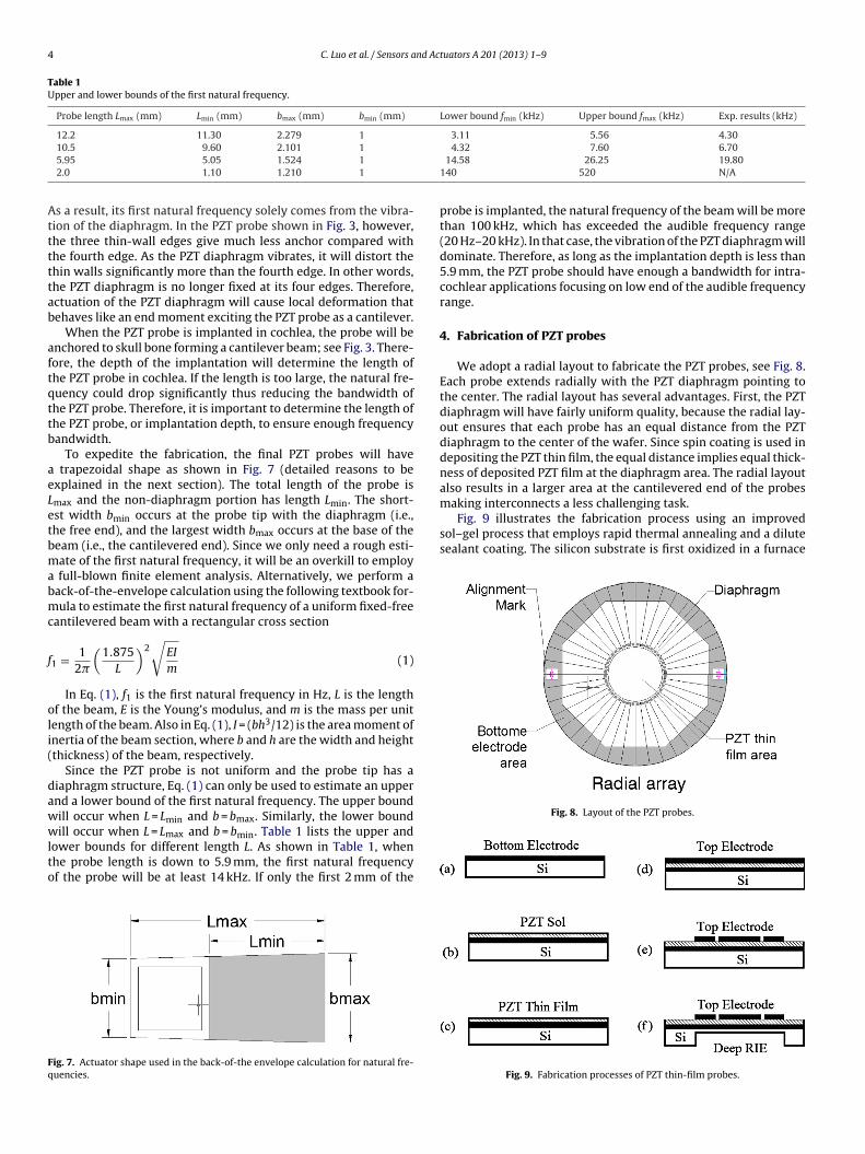
making interconnects a less challenging task.Fig. 9 illustrates the fabrication process using an improved
sol–gel process that employs rapid thermal annealing and a dilutesealant coating. The silicon substrate is first oxidized in a furnace
Fig. 8. Layout of the PZT probes.
10.5 9.60 2.101 1
5.95 5.05 1.524 1
2.0 1.10 1.210 1
s a result, its first natural frequency solely comes from the vibra-ion of the diaphragm. In the PZT probe shown in Fig. 3, however,he three thin-wall edges give much less anchor compared withhe fourth edge. As the PZT diaphragm vibrates, it will distort thehin walls significantly more than the fourth edge. In other words,he PZT diaphragm is no longer fixed at its four edges. Therefore,ctuation of the PZT diaphragm will cause local deformation thatehaves like an end moment exciting the PZT probe as a cantilever.
When the PZT probe is implanted in cochlea, the probe will benchored to skull bone forming a cantilever beam; see Fig. 3. There-ore, the depth of the implantation will determine the length ofhe PZT probe in cochlea. If the length is too large, the natural fre-uency could drop significantly thus reducing the bandwidth ofhe PZT probe. Therefore, it is important to determine the length ofhe PZT probe, or implantation depth, to ensure enough frequencyandwidth.
To expedite the fabrication, the final PZT probes will have trapezoidal shape as shown in Fig. 7 (detailed reasons to bexplained in the next section). The total length of the probe ismax and the non-diaphragm portion has length Lmin. The short-st width bmin occurs at the probe tip with the diaphragm (i.e.,he free end), and the largest width bmax occurs at the base of theeam (i.e., the cantilevered end). Since we only need a rough esti-ate of the first natural frequency, it will be an overkill to employ
full-blown finite element analysis. Alternatively, we perform aack-of-the-envelope calculation using the following textbook for-ula to estimate the first natural frequency of a uniform fixed-free
antilevered beam with a rectangular cross section
1 = 12�
(1.875
L
)2√
EI
m(1)
In Eq. (1), f1 is the first natural frequency in Hz, L is the lengthf the beam, E is the Young’s modulus, and m is the mass per unitength of the beam. Also in Eq. (1), I = (bh3/12) is the area moment ofnertia of the beam section, where b and h are the width and heightthickness) of the beam, respectively.
Since the PZT probe is not uniform and the probe tip has aiaphragm structure, Eq. (1) can only be used to estimate an uppernd a lower bound of the first natural frequency. The upper boundill occur when L = Lmin and b = bmax. Similarly, the lower bound
ill occur when L = Lmax and b = bmin. Table 1 lists the upper andower bounds for different length L. As shown in Table 1, whenhe probe length is down to 5.9 mm, the first natural frequencyf the probe will be at least 14 kHz. If only the first 2 mm of the
ig. 7. Actuator shape used in the back-of-the envelope calculation for natural fre-uencies.
4.32 7.60 6.7014.58 26.25 19.80
140 520 N/A
probe is implanted, the natural frequency of the beam will be morethan 100 kHz, which has exceeded the audible frequency range(20 Hz–20 kHz). In that case, the vibration of the PZT diaphragm willdominate. Therefore, as long as the implantation depth is less than5.9 mm, the PZT probe should have enough a bandwidth for intra-cochlear applications focusing on low end of the audible frequencyrange.
4. Fabrication of PZT probes
We adopt a radial layout to fabricate the PZT probes, see Fig. 8.Each probe extends radially with the PZT diaphragm pointing tothe center. The radial layout has several advantages. First, the PZTdiaphragm will have fairly uniform quality, because the radial lay-out ensures that each probe has an equal distance from the PZTdiaphragm to the center of the wafer. Since spin coating is used indepositing the PZT thin film, the equal distance implies equal thick-ness of deposited PZT film at the diaphragm area. The radial layoutalso results in a larger area at the cantilevered end of the probes
Fig. 9. Fabrication processes of PZT thin-film probes.

C. Luo et al. / Sensors and Actuators A 201 (2013) 1– 9 5
aa(trF1aTttotiiptd
ttaPSfieaFw
iDpiholdf
ttpIeaa4a
af
Fig. 11. Photo of a fabricated PZT thin-film microactuator probe.
in water. These tests and their results are explained in detail asfollows.
Fig. 10. Blowup view of the mask used in DRIE (units: �m).
t 1045 ◦C for 2 h to grow a SiO2 layer of 500 nm thick. Then layer silicon nitride of 200 nm thick is deposited by PECVDplasma enhanced chemical vapor deposition). The bottom elec-rode consists of Pt/Ti layers with thickness of 100 nm and 50 nm,espectively (Fig. 9(a)). The PZT film is spin-coated three times.or the first two coatings, the sintering temperature is 650 ◦C for5 min. For the third coating, the sol is diluted 50% by acetic acidnd sintering temperature is 450 ◦C for 10 min (Fig. 9(b) and (c)).he top electrode layer consists of Au/Cr layers through evapora-ion (Fig. 9(d)). The top electrode layer is then patterned to formhe center and outer electrodes (Fig. 9(e)). Finally, the backsidef the silicon is etched via deep reactive ion etch (DRIE) to formhe diaphragm suspension (Fig. 9(f)). The thickness of the PZT films measured around 1 �m. Please note that the schematic draw-ngs in Fig. 9 mainly illustrate the fabrication process of the PZTrobes (e.g., electrodes and diaphragms). Mechanisms to releasehe PZT probes from the wafer are not included in Fig. 9 and will beiscussed later in detail.
Now let us explain how the fabrication process in Fig. 9 works inhe context of the radial layout in Fig. 8. First of all, a bottom elec-rode is deposited over the entire wafer (cf. Fig. 9(a)). Then the grayrea along the perimeter in Fig. 8 is shielded with blue tapes. Next,ZT thin film is deposited using spin coating (cf. Fig. 9(b) and (c)).ince part of the bottom electrode is taped, the resulting PZT thinlm will only appear over the white, octagonal area of Fig. 8. Toplectrodes are then fabricated onto the PZT thin film (cf. Fig. 9(d)nd (e)). (Note that the top electrodes are not explicitly shown inig. 8.) Finally, DRIE is used to form the PZT diaphragms (cf. Fig. 9(f)),hich appear as tiny dark squares in Fig. 8.
The PZT probes are simultaneously released from the wafer dur-ng the step of DRIE. Fig. 10 shows a blowup view of the mask used inRIE. The gray area is the etch-away portion by DRIE, and the whiteortion defines the resulting PZT probes. The etch-away portion
ncludes two parts. The first part is the square diaphragms, whichave already been explained extensively in Figs. 8 and 9(f). The sec-nd part is release slots that are either radial or circular in shapeocating around each PZT probe. (These release slots also appear asark radial lines and circle in Fig. 8.) They are explained in detail asollows.
These release slots around each PZT probe are very critical. Athe end of DRIE, not only are the PZT diaphragms formed but alsohese slots that gently support the PZT probes. At this time, the PZTrobes can be easily released from the wafer by breaking these slots.
n order to break these slots easily, the width of the slots needs toxceed a critical value. After a few trials and errors, we find that
slot width of at least 200 �m is needed. Fig. 11 shows photos of released PZT probe. In general, the thickness of the PZT probe is00 �m, while the thickness h of the diaphragm is roughly 2–3 �m
s designed in Fig. 3.After the probes are released, they are placed in a special fixturend secured via Silicone; see Fig. 12. The released probes have dif-erent protrusion portions in the fixture to mimic the implantation
Fig. 12. Fixture holding released probes for parylene packaging.
depths. The fixture and the probes are then packaged with confor-mal parylene coating. Fig. 13 shows cross sectional view of a PZTprobe at the diaphragm area. The thickness of the parylene coatingis 0.25 �m. Based on the calculation in Fig. 6, the 0.25-�m thickparylene will reduce actuator displacement no more than 5%. Afterthe packaging, the PZT probes along with the Silicone can be easilyreleased from the fixture for testing.
5. Experimental measurements
After the PZT probes are packaged, they are tested in air and
Fig. 13. Cross sectional views of the PZT diaphragm packaged with parylene.

6 C. Luo et al. / Sensors and Actuators A 201 (2013) 1– 9
Table 2Displacement and natural frequency of PZT probes before and after parylene package is coated.
Device Displacement Natural frequency
Before coating (nm/V) After coating (nm/V) Variation (%) Before coating (kHz) After coating (kHz) Variation (%)
1 10.18 9.95 97.74 59.79 58.19 97.34
5
oib(
abtP
aesPPmf
F
2 11.38 11.32 99.473 12.65 12.50 98.814 14.73 14.45 98.10
.1. Tests in air
The purpose of the tests is to establish a reference measurementf a PZT probe before it goes into a functional test in water. Specif-cally, the tests allow us to identify proper implantation depth andoundary conditions to maintain the bandwidth of the PZT probecf. Section 3.2).
Fig. 14 shows a PZT probe and its setup. The PZT probe is fixed ton aluminum block at its base via epoxy. The amount of epoxy cane added incrementally; see epoxy 1 to epoxy 4 in Fig. 14. By varyinghe amount of epoxy, we can control the implantation depth of theZT probe in the experiments.
The experimental setup includes a spectrum analyzer, an AVCmplifier to drive piezoelectric load, and a laser Doppler vibrom-ter (LDV). A source in the spectrum analyzer generates a sweptine signal to the AVC amplifier, which subsequently drives the
ZT probe. In the meantime, the LDV measures velocity of theZT diaphragm at its center. The swept sine voltage and the LDVeasurement are processed by the spectrum analyzer to generaterequency response functions (FRFs) of the PZT probe. Fig. 15 shows
Fig. 14. A PZT probe and its experimental setup.
ig. 15. Measured frequency response functions at various implantation depths.
58.82 57.75 98.1856.91 54.87 96.4258.38 56.42 96.64
some measured FRFs. The measurements clearly indicate that ashorter implantation depth results in a higher natural frequency.
Table 1 also compares the measured natural frequency withthe theoretical predictions using the back-of-the-envelope calcula-tions. The comparison shows that the measured natural frequenciesnicely fall within the upper and lower bounds predicted from theback-of-the-envelope calculations.
Table 2 compares the measured displacement and natural fre-quency of several PZT probes before and after the parylene packageis coated. Experimental results show that the parylene coatingreduces the displacement and the natural frequency no more than3% and 4%, respectively.
5.2. Tests in water
Packaged and unpackaged PZT probes are submerged in deion-ized (DI) water for performance tests. Two types of tests areconducted. One is impedance test. Basically, one top electrode(either the center or the outer electrode) and the bottom electrodesare connected to an impedance analyzer to measure the impedanceof the PZT probe. The other test is the LDV measurement describedin Section 5.1. Since the LDV compares the reflected beam with areference beam to obtain its measurement, the measured veloc-ity will depend on the index of refraction of the medium throughwhich the laser beam has traveled. When the test is conducted inthe water, the measurements have to be divided by the index ofrefraction in order to obtain the true velocity of the PZT probe.
As a reference, Fig. 16 shows measured impedance (both mag-nitude and phase) of an unpackaged PZT probe when submerged inDI water. The impedance is measured from the center electrode tothe bottom electrode. The impedance magnitude and phase mea-surements refer to the left and right axes, respectively. When theunpackaged PZT probe is in air, the phase is nearly 90◦ (−89◦ to beexact) indicating that the resistance is very large and the systemis nearly a capacitor. When the unpackaged probe is submerged in
water, the impedance magnitude drops significantly, and the phasechanges to −77◦, implying that the surrounding water has affectedthe PZT probe by substantially reducing the resistance. When theprobe is taken out of the water, the impedance returns to its originalFig. 16. Measured impedance (magnitude and phase) of an unpackaged PZT probesubmerged in deionized water.

C. Luo et al. / Sensors and Actuators A 201 (2013) 1– 9 7
Fm
vo
emnpfTtieii
Pmaorl5bd12aaodp
Fm
ig. 17. Measured impedance (magnitude and phase) of a packaged PZT probe sub-erged in deionized water.
alue. Also, the change of impedance, when the probe is in and outf the water, is immediate.
In comparison, Fig. 17 shows the impedance (center to bottomlectrodes) of a PZT probe packaged with parylene when sub-erged in and taken out of DI water. First of all, the impedance does
ot experience a sudden change as in the case of the unpackagedrobe. Moreover, the phase of the impedance changes only slightlyrom −89◦ to −88◦, even the packaged probe is in the water for 5 h.his indicates that the parylene package has protected the elec-rodes and the PZT thin film reasonably well and very little energys lost to the surrounding water. The impedance magnitude, how-ver, decreases gradually once the packaged probe is submergedn water. This indicates that the surrounding water has somehowncreased the capacitance of the PZT probe.
Fig. 18 shows the measured displacement when the packagedZT probe is submerged in the water. Specifically, the measure-ents come from FRFs measured via the LDV and the spectrum
nalyzer. The data points presented in Fig. 18 are the magnitudef FRFs at 3 kHz. Three rounds of experiments are conducted forepeatability. The first round of experiment is to test the enduranceimit of the probe, so the displacement is measured at 28, 31, and4 h. (These data are crammed into Fig. 18 for reference, denotedy the cross markers.) In the second round of the experiment, theisplacement is measured more frequently (e.g., half-and-hour or-hour increments) after the probe is submerged in the water to4 h. The measured displacement starts to increase from 10 nm/Vs the packaged PZT probe is submerged in water, and saturatesround 22 nm/V in about 2 h to a steady value. The third round
f experiment focuses on the first 2 h to ensure that the measuredisplacement is repeatable. Experimental results show that the dis-lacement indeed increases in the first 2 h. The blowup view inig. 18. Measured displacements (via LDV) of a packaged PZT probe when sub-erged in water.
Fig. 19. Measured impedance (magnitude and phase) of a packaged PZT probe sub-merged in deionized water; 0–5 h.
Fig. 18 shows the measured results for the first 2 h. To ensure thatthis displacement increase is not from thermal drift of the LDV, weconduct a separate experiment in the air for 2 h. The measured dis-placement remains at 10 nm/V. So the displacement increase is notfrom the thermal drift of the LDV.
The impedance measurements also support the observation thatthe displacement increases in the first 2 h. Fig. 19 shows a blowupview of the impedance measurements from the center to bottomelectrodes shown in Fig. 17 for the first 5 h. Initially, the impedancemagnitude drops at a faster rate, and gradually stabilizes around2 h. Specifically, in the first 2 h, the impedance magnitude drops ata rate of 264 ohm/h. After 2 h, the impedance magnitude drops at arate of 167 ohm/h. Something must have happened in the first 2 hin order to account for the nearly 100 ohm/h difference. This agreeswith the observation that the displacement has changed in the first2 h.
In interpreting the impedance measurements, it is more impor-tant to compare the impedance difference between two timeintervals instead of the absolute measured values of the impedancefor the following reason. Since the interconnects—where theimpedance measurements are taken—are located at the far endfrom the PZT diaphragm, the PZT diaphragm and the lead wires(including the interconnects) on the probe all contribute to themeasured impedance. As shown in Fig. 12, the far ends of the PZTprobes are embedded in Silicone in the fixture while parylene iscoated. When the PZT probes, together with the Silicone, are takenout of the fixture, certain surfaces of the Silicone are not coatedwith parylene. Therefore, when the entire PZT probe is submergedin a Petri dish of water, the water gradually soak into the Sili-cone increasing the dielectric constant of the Silicone causing the
impedance to drop.With this background information, it is obvious that the fasterimpedance drop in the first 2 h implies that the impedance of thePZT diaphragm has dropped in the first 2 h and eventually saturates
Fig. 20. Schematic drawing of the hypothesis.

8 C. Luo et al. / Sensors and Actuators A 201 (2013) 1– 9
ectrod
adAtftme
5
in
m(TTwotwTrt
ichvt
Fsfc3achtipWwsisfid
Fig. 21. High-magnification SEM images; (left) PZT surface before top el
t the end of the 2 h. When the impedance of the PZT diaphragmrops, the electric current supplied to the PZT diaphragm increases.ccording to the constitutive equation of linear piezoelectricity,
his means that the displacement has to increase. Therefore, theaster impedance drop in Fig. 19 for the first 2 h is consistent withhe displacement increase in Fig. 18 for the first 2 h. The displace-
ent increase is a real phenomenon; it is not a measurementrror.
.3. Hypothesis and evidence
It is by all means counter-intuitive that a PZT probe actuallyncreases its displacement when it is submerged in the water. Aatural question is what causes this phenomenon.
From a broader picture, there are two mechanisms that aechanical system can increase its displacement at a frequency
e.g., 3 kHz) far lower than its natural frequency (e.g., 80 kHz).he first mechanism is that the stiffness of the system is reduced.his is rather unlikely, because there are no obvious sources thatould reduce the stiffness of the PZT probe in the water. More-
ver, stiffness is inversely proportional to the displacement. Sincehe displacement has changed from 10 nm/V in air to 22 nm/V inater, it implies a more than 50% reduction of stiffness in the water.
here are no known mechanisms causing such a significant stiffnesseduction in water in such a short time scale. Therefore, we rule outhis possibility.
The second mechanism is that the excitation to the system hasncreased. According to the impedance measurements in Fig. 19, theapacitance (and thus the dielectric constant) of the PZT diaphragmas increased in the first 2 h. This implies that excitation per unitoltage applied to the PZT diaphragm has increased. But where doeshe increase of dielectric constant come from?
We hypothesize that water has infiltrated into the PZT thin film.ig. 20 shows a schematic drawing of the hypothesis. As we know,ol–gel derived PZT thin films tend to be porous. Nano-channelsorm under the porous PZT surface as a result of the sol–gel pro-esses. When the top electrode is deposited at a pressure around
× 10−6 torr, the deposition is unidirectional. Therefore, only therea directly facing the pores is covered with the top electrode. Inontrast, the parylene molecules, deposited at a pressure of 0.1 torr,ave a much smaller mean free path in the deposition chamber;herefore, the parylene coating is omni-directional. Therefore, allnterior surfaces will be coated with parylene, and the presence ofarylene successfully insulates the top electrodes from the water.hen the PZT probe is tested in air, the nano-channels are filledith air (dielectric constant ≈1) resulting in a low dielectric con-
tant of the PZT thin film (about 270). When the PZT probe is tested
n water, the nano-channels are filled with water (dielectric con-tant ≈80), thus increasing the dielectric constant of the PZT thinlm resulting in larger excitation to and displacement of the PZTiaphragm.es are coated, and (right) PZT surface after top electrodes are deposited.
To support the hypothesis, we have taken SEM image usinga 200,000× magnification; see Fig. 21. The images on the left(200,000× and 40,000×) are taken immediately after the PZT thinfilm is deposited. The images on the right (200,000× and 40,000×)are taken immediately after the top electrodes are deposited ontothe PZT thin film. All the SEM images show numerous pores on thesurface allowing water molecules to infiltrate.
6. Conclusions
In this paper, we have successfully designed, fabricated, andtested a PZT thin-film microactuator probe that can be potentiallyimplanted in cochlea for animal trials. For the design phase of thePZT probes, the finite element simulations show that reduction ofactuator displacement due to the parylene package is less than 3% ifthe thickness of parylene is 0.25 �m. The back-of-the-envelope cal-culation ensures that the actuator bandwidth exceeds the audiblefrequency range when the implantation length is less than 5.9 mm.For the fabrication phase of the PZT probes, the radial mask layoutsturn out to be very effective. Using DRIE as a release mechanism todice the fabricated PZT probes off the wafer is a success. Use of aholder fixture proves to be important when handling the PZT probesbefore, during, and after the parylene deposition. For the testingphase of the research, it proves to be critical to have both LDV andimpedance measurements in order to understand the complicatedphysics associated with the PZT probes. When submerged in water,the tested PZT probe functions normally for 55 h without failure,indicating that the parylene package is indeed functional. More-over, the PZT probe increases its displacement in the first 2 h as aresult of an increase of its dielectric constant. This phenomenon canbe well supported via a hypothesis that water molecules have infil-trated into the PZT thin film due to nano-pores on the film surfaceas a result of sol–gel processes.
Acknowledgments
This material is based upon work supported by the NationalScience Foundation under Grant No. CBET-1159623. Any opinions,findings, and conclusions or recommendations expressed in thismaterial are those of the authors and do not necessarily reflect theviews of the National Science Foundation.
References
[1] B.J. Gantz, C. Turner, K.E. Gfeller, M.W. Lowder, Preservation of hearing incochlear implant surgery: advantages of combined electrical and acousticalspeech processing, The Laryngoscope 115 (2005) 796–802.
[2] B.S. Wilson, D.T. Lawson, J.M. Muller, R.S. Tyler, J. Kiefer, Cochlear implants:
some likely next steps, Annual Review of Biomedical Engineering 5 (2003)207–249.[3] M.F. Dorman, R.H. Gifford, Combining acoustic and electric stimulation in theservice of speech recognition, International Journal of Audiology 49 (2010)912–919.

nd Ac
[
[
[
[
[
[
[
[
[
[
[
[
[
[
[
[
[
[
[
[
[
[
[
[
[
[
[
[
[38] M. Olfatnia, T. Xu, et al., Piezoelectric circular microdiaphragm based pressure
C. Luo et al. / Sensors a
[4] C.C. Lee, C.R. Hume, G.Z. Cao, I.Y. Shen, Development of PZT thin-film microac-tuators for hybrid cochlear implants, in: Abstracts of 2005 Conference onImplantable Auditory Prostheses, Asilomar, CA, USA, August 1–4, 2005.
[5] C.C. Lee, C.R. Hume, G.Z. Cao, I.Y. Shen, A feasibility study of PZT thin-filmmicroactuators for hybrid cochlear implants, in: Proceedings of 27th AnnualInternational Conference of the IEEE Engineering in Medicine and Biology Soci-ety, Paper #1034, Shanghai, China, September 1–4, 2005.
[6] C.C. Lee, Q. Guo, G.Z. Cao, I.Y. Shen, Effect of electrode size and silicon residueon piezoelectric membrane actuators, Sensors and Actuators A-Physical 147(2008) 279–285.
[7] C.C. Lee, C.R. Hume, G.Z. Cao, I.Y. Shen, Temporary packaging of PZT thin-filmmicroactuators, Integrated Ferroelectrics 101 (2009) 121–131.
[8] C.-C. Lee, G.Z. Cao, I.Y. Shen, Effects of residual stresses onlead–zirconate–titanate (PZT) thin-film membrane microactuators, Sensorsand Actuators A—Physical 159 (2010) 88–95.
[9] G.Z. Chuan Luo, I.Y. Cao, Shen, Enhancing displacement of lead-zirconate-titanate (PZT) thin-film membrane microactuators via a dual electrode design,Sensors and Actuators A—Physical 173 (2012) 190–196.
10] Y. Choe, L. Wang, et al., On-chip integration of eight directional droplet ejectorsfor inking a spot with eight droplets without ejector movement, in: Interna-tional Solid-State Sensors, Actuators and Microsystems Conference, 2011.
11] M. Kagerer, D. Rumschoettel, et al., Fabrication and application of a chemicalresistant low-cost microdrop generator, in: International Mechanical Engineer-ing Congress and Exposition, IMECE, 2011.
12] Y. Luo, M. Lu, et al., A polymer-based bidirectional micropump driven by a PZTbimorph, Microsystem Technologies 17 (3) (2011) 403–409.
13] H.-K. Ma, J.-S. Wang, et al., The performance of a novel pseudo-bipolar bi-cellpiezoelectric proton exchange membrane fuel cell with a smaller nozzle anddiffuser, Journal of Power Sources 196 (18) (2011) 7564–7571.
14] E. Sayar, B. Farouk, Multifield analysis of a piezoelectric valveless micropump:Effects of actuation frequency and electric potential, Smart Materials and Struc-tures 21 (7) (2012).
15] U. Baran, D. Brown, et al., Resonant PZT MEMS scanner for high-resolutiondisplays, Journal of Microelectromechanical Systems 21 (6) (2012) 1303–1310.
16] K.H. Gilchrist, D.E. Dausch, et al., Electromechanical performance of piezoelec-tric scanning mirrors for medical endoscopy, Sensors and Actuators, A: Physical178 (2012) 193–201.
17] K.H. Koh, T. Kobayashi, et al., Novel piezoelectric actuation mechanism for agimbal-less mirror in 2D raster scanning applications, Journal of Micromechan-ics and Microengineering 21 (7) (2011).
18] S. Matsushita, I. Kanno, et al., Metal-based piezoelectric microelectromechani-cal systems scanner composed of Pb(Zr, Ti)O3 thin film on titanium substrate,Microsystem Technologies 18 (6) (2012) 765–771.
19] S. Yuana, W. Liu, et al., Analysis and test of an optical scanner actuated by PZTfilms, in: 6th China International Conference on High-Performance Ceramics,CICC-6, August, 2009.
20] E.-H. Yang, Y. Hishinuma, et al., Thin-film piezoelectric unimorph actuator-based deformable mirror with a transferred silicon membrane, Journal ofMicroelectromechanical Systems 15 (5) (2006) 1214–1225.
21] M.A. Matin, D. Akai, et al., Characterization of the deflection of a new epitaxial
piezoelectric micro-mirror: modeling and experiment, Materials Science andEngineering B: Solid-State Materials for Advanced Technology 175 (2) (2010)129–135.22] M. Sato, S. Tsuda, et al., Development of piezoelectric MEMS deformable mirror,Springer Verlag, Heidelberg, Germany, 2010, Tiergartenstrasse 17, D-69121.
[
tuators A 201 (2013) 1– 9 9
23] Y. Choe, S. Chen, E.S. Kim, High fidelity loud microspeaker based on PZT bimorphdiaphragm, in: NSTI Nanotechnology Conference and Expo, February, 2010, pp.316–319.
24] J. Cho, S. Jang, H. Nam, A piezoelectrically actuated mems speaker withpolyimide membrane and thin film pb(zr ti)o3(pzt) actuator, Integrated Fer-roelectrics 105 (2) (2009) 7–36.
25] X. Ting, M. Jianmin, et al., Investigation of the effect of adsorption inducedsurface stress on the resonant frequency of PZT membrane based biosensors,in: 2010 5th IEEE International Conference on Nano/Micro Engineered andMolecular Systems (NEMS 2010), 20–23, January, 2010.
26] S. Li, W. Ren, et al., Ferroelectric thin film diaphragm resonators for bio-detection, in: 12th International Meeting on Ferroelectricity, IMF-12 and the18th IEEE International Symposium on Applications of Ferroelectrics, ISAF-18,August, 2009.
27] D.F. Wang, X. Li, et al., Ring-shaped PZT film resonator for bio-sensing appli-cations in liquid environment, in: 25th Eurosensors Conference, September,2011.
28] I.O.M. Kanja, et al., High sensitivity ultrasonic transducer array for 2-Dhydrop0hone application, using an epitaxial PZT thin film grown on -Al2O3/Si, in: 15th International Conference on Solid-State Sensors, Actuators andMicrosystems, June, 2009.
29] G.L. Smith, R.Q. Rudy, et al., Integrated thin-film piezoelectric traveling waveultrasonic motors, in: 16th International Solid-State Sensors. Actuators andMicrosystems Conference, June, 2011.
30] I. Ahmed, D. Halupka, et al., A 3-axis PZT-based MEMS gyroscope in 0.18 mCMOS, in: 38th European Solid State Circuits Conference, ESSCIRC, September,2012.
31] E. Fuentes-Fernandez, L. Baldenegro-Perez, Optimization ofPb(Zr0.53,Ti0.47)O3 films for micropower generation using integratedcantilevers, Solid-State Electronics 63 (1) (2011) 89–93.
32] I. Kuehne, M. Schreiter, et al., A novel MEMS design of a piezoelectric generatorfor fluid-actuated energy conversion, in: Smart Sensors, Actuators, and MEMSV, April, 2011.
33] I. Kanno, T. Ichida, et al., Power-generation performance of lead-free(K,Na)NbO3 piezoelectric thin-film energy harvesters, Sensors and Actuators,A 179 (2012) 132–136.
34] S. Kimura, S. Tomioka, et al., Improved performances of acoustic energy har-vester fabricated using sol/gel lead zirconate titanate thin film, Japanese Journalof Applied Physics 50 (6 (Part 2)) (2011).
35] K. Wasa, T. Matsushima, et al., Thin-film piezoelectric materials for a betterenergy harvesting MEMS, Journal of Microelectromechanical Systems 21 (2)(2012) 451–457.
36] D. Isarakorn, D. Briand, et al., Finite element analysis and experiments ona silicon membrane actuated by an epitaxial PZT thin film for localized-mass sensing applications, Sensors and Actuators, B 153 (1) (2011)54–63.
37] D.G. Hwang, Y.M. Chae, et al., Fabrication and characterization of PZT (lead zir-conate titanate) bridge-shaped resonator for mass sensing application, Journalof Electroceramics 29 (3) (2012) 225–234.
sensors, Sensors and Actuators, A 163 (1) (2010) 32–36.39] E. Heinonen, J. Juuti, et al., High performance thin film PZT ultrasonic transducer
by CSD for distance measurements in water, Journal of Electroceramics 27 (1)(2011) 24–28.