sequential plasma activated process for silicon …mrhowlader/publications/sequnetial...
TRANSCRIPT
Sequential Plasma Activated Process for Silicon Direct Bonding
M. M. R. Howladera, T. Sugab, H. Itohb, M. J. Kimc
a Engineering Physics Department, and Electrical and Computer Engineering Department, McMaster University, Hamilton, Ontario L8S 4L7, Canada
b Department of Precision Engineering, The University of Tokyo, Tokyo 113-8656, Japan c Department of Electrical Engineering, University of Texas at Dallas, Texas, USA
Sequential plasma activated bonding (SPAB) process consisting of oxygen reactive ion etching (RIE) and nitrogen microwave radical plasma was developed for silicon direct bonding at room temperature. A strong influence of plasma time and gas pressure on voids was found both in the SPAB and O2 RIE processes. Tensile strength and surface roughness are functions of oxygen RIE, nitrogen radical time and gas pressure. Improved tensile strength was achieved in the SPAB process. High resolution transmission electron microscope (HRTEM) observations showed a thicker silicon oxide interfacial layer from the SPAB process than that from the O2 RIE process. The increase in thickness of interfacial oxide layers in both processes after annealing at 600°C for 2 h in air is attributed to the oxygen concentration of silicon bulk wafers. The SPAB process can be explained by the reaction between two metastable surfaces, which allows water removal from interface, resulting in covalent Si-O-Si bonding.
Introduction Silicon direct bonding (SDB) refers to joining two flat, mirror-polished, and clean silicon surfaces by different direct bonding techniques, such as hydrophilic, hydrophobic, fusion, and plasma activation bonding. Hydrophilic surfaces are prepared by cleaning the wafers in RCA1 solution (NH4OH:H2O2:H2O=1:1:5) for removing organic contaminants, and sometimes in RCA2 solution (HCl:H2O2:H2O=1:1:6) for removing metal and alkaline contaminants (1). Hydrophilic surfaces are covered by a native oxide and a high density of OH groups. The hydrophilic surfaces changes into hydrophobic surfaces if they are dipped in HF acid. In this case, the surfaces are terminated with hydrogen. Hydrophilic and hydrophobic bonding processes for silicon rarely refer to fusion bonding (2), but this name is misleading because the process temperatures are in the range of 700-1000°C, which are used for the enhancement of bonding energy. These temperatures are lower than the fusion point of Si, which is 1400 °C.
In plasma activation bonding, reactive ion etching (RIE) (3,4), inductively coupled plasma (ICP) (5,6), and ultra-violet (UV) (7) radiation plasma are carried out in different atmospheres such as Ar, O2, N2, and H2. Sometimes plasma and RCA treated surfaces need to be dipped in H2O to increase the number of OH molecules on the surfaces. Due to the termination of OH (for hydrophilic and plasma) and H (hydrophobic), the processed surfaces need to be heated after contact to enhance the bonding energy. While the hydrophilic and plasma bonded surfaces produce an amorphous interface layer of SiO2 after heating, the hydrophobic bonded Si/Si surfaces result in Si-Si covalent bonding at the interface as in bulk Si. The bonded wafers by plasma process have been heated at
ECS Transactions, 3 (6) 191-202 (2006)10.1149/1.2357070, copyright The Electrochemical Society
191
192
lower (200-400°C) (3-7) temperatures than those made by hydrophilic and hydrophobic bonding processes (500-1000°C) (1,2,8). Further reduction of the temperature in the plasma bonding processes allows for the alleviation of heating problems, such as alignment difficulty, gas formation in the cavity, and damage of temperature-sensitive active and passive structures. In addition, the process complexities, such as a dip in water or RCA clean, after plasma treatment should be avoided. Therefore, the development of a chemical free room temperature (RT) plasma bonding process is indispensable.
A plasma bonding process has been developed by combining the effects of physical sputtering of oxygen RIE and chemical reactivity of nitrogen MW radical on the same surface at RT. This is a two step surface activation method, called sequential plasma activated bonding (SPAB) process (9). The physical sputtering of O2 RIE plasma removes surface contaminants and oxidizes surfaces. Subsequent processing using N2 radical generates chemically unstable silicon surfaces. After exposing the surfaces in ambient, the combined effect of oxygen plasma and N2 radical enhances bonding strength equivalent to the hydrophobic and hydrophilic bonding processes. The strong bonding strength is due to spontaneous reactions between the metastable surfaces. The advantage of the method is the capability to bond delicate micro-electro-mechanical system (MEMS), and diverse temperature-sensitive components and devices without high external load. It also allows bonding at RT. The SPAB process has been successfully applied for wafer-level bare silicon/silicon (9), glass/glass (10,11), and patterned Si/glass bonding (11) at RT. The article presents further insights into the bonding mechanism of silicon/silicon bonding using the SPAB process at RT.
Experimental Procedure
P-type double side mirror polished Czochralsky (CZ) grown (100) Si wafers with a thickness of 725 µm were used. The resistance of the wafers was 25-30 Ohm. Wafer surfaces were activated in a low vacuum pressure using a 13.85 MHz oxygen radio frequency (RF) plasma followed by 2.45 GHz N2 MW plasma at room temperature. Before surface activation using the SPAB process and O2 RIE plasma, the wafers were not dipped in wet chemical and water. In the case of MW plasma, a system to extract electrically neutral radicals was developed. Radicals can chemically activate the wafer surfaces. On the other hand, ions generated in RIE in the RF plasma were accelerated by self-bias voltage to increase physical bombardment capability. The plasma source powers were 200 and 2000 W, respectively for the RF and MW plasma.
For sequential activation, the wafer surfaces were processed by oxygen RIE plasma for 60 s at 30 Pa and then subsequently processed by additional nitrogen radicals for 60 s at 30 Pa unless mentioned otherwise. In order to generate RIE plasma and radicals in one chamber, an RF discharge electrode and an ion-trapping metal plate for MW plasma were used as shown in figure 1. In this configuration, RIE plasma is generated by the discharge between the ion trapping metal plate and the RF electrode (Fig. 1a). MW plasma was generated and passed through the ion-trapping metal plate to generate a neutralized nitrogen beam (charge-free radicals) by absorbing ions in the holes of the metal plate (Fig. 1b). By the help of the independent plasma generation with the MW and RF discharge systems, a wafer surface can be activated by ions with high bombardment energy, and by radicals without bombardment energy in one plasma chamber. Oxygen gas for RIE plasma and nitrogen gas for radical generation were used. Tables I and II show the plasma generating conditions and surface activation parameters for different experiments.
ECS Transactions, 3 (6) 191-202 (2006)

193
Figure 1. Schematic diagrams for sequential plasma activated bonding (SPAB) process consisting of (a) O2 RIE plasma system with self-biased condition and (b) N2 MW radical plasma. In the SPAB process, O2 RIE plasma was generated followed by N2 radical extracted from MW plasma. The chamber pressure was 10 Pa.
After surface activation, the wafers were contacted under hand-applied pressure outside the vacuum chamber in a clean room atmosphere at room temperature. Finally the contacted wafers were cold rolled under 100 kg to remove air trapped across the interface. Bulk equivalent high bonding strength was found after 24h. Table I. Experimental conditions of plasma parameters in the O2 RIE plasma activated bonding process. Plasma Power [W] Time [s] Pressure [Pa]
10 30 – – – 60 30 50 75 100 300 30 – – –
200
1200 30 – – – Table II. Plasma parameters used in the sequential plasma activated bonding (SPAB) process. In the SPAB process, the wafer surfaces were activated by O2 RIE plasma for 60 s at 30 Pa followed by N2 MW radical treatment at different time and gas pressure.
Mode Plasma Power [W] Time [s] Pressure [Pa]
O2 RIE Plasma 200 60 30 30 30 30
10 30 – – – 60 30 50 75 100 300 30 – – –
N2 MW Radical 2000
1200 30 – – –
N2 N2
Exhaust
MW Plasma
Sample
Glass plate
2.45 GHz Micro wave
Rectangular waveguide
Radicals Ion trapping plate
Surface wave Plasma
(b)
O2 O2
Exhaust
RF Plasma Sample
Electrode
Ion trapping plate Glass plate
13.56 MHz Radio Frequency
Matching Box
(a)
ECS Transactions, 3 (6) 191-202 (2006)

194
Results and Discussion
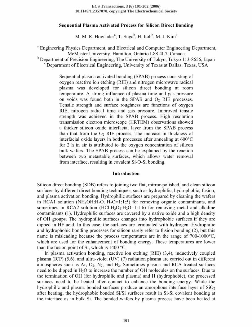
Plasma processing time and gas pressure of O2 RIE and N2 radical plasma are the main controlling parameters for bonding. To investigate the influence of process parameters on the activation of wafer surfaces and bonding quality, we investigated the bonded interfaces using infrared transmission images, tensile strength, surface roughness, and mcorstructural observation as a function of activation time and gas pressure. Since the SPAB process consists of physical activation using O2 RIE plasma and chemical activation using the N2 radical, we carried out a comparative study of the results in insights in relation to the bonding mechanism of silicon/silicon. Figure 2 shows the nitrogen radical time and gas pressure dependence on Si/Si interface using infrared transmission observation.
Infrared (IR) Transmission Images.
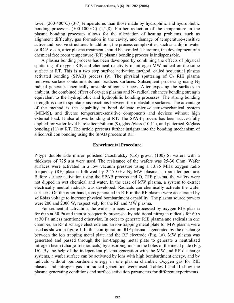
A number of voids can be seen at the peripheral region of the bonded interface. The number of voids was higher at the peripheral regime than at the center area. Insufficient surface activation of the peripheral region compared to the central surface area and wafer warpage during activation are most likely responsible for void generation at periphery. Although the number of voids was increased, as shown in Fig. 2(a) and (b), there was no strong correlation between the nitrogen radical time and pressure, and the voids in the SPAB process. In O2 RIE process, the number of voids and the size of the voids increased as a function of plasma processing time and gas pressure, as shown in Fig. 3(a) and (b), which is in contrast to the SPAB process. Generally voids form due to the trapped air and small particles during bonding across the interface (7,12). But it is unlikely here that the presence of small particles and trapped air is the cause of void generation because we bonded the wafers at identical ambient conditions except for the changes in the process parameters of O2 RIE and N2 radical. Weigand et al. (13) suggested that the increase of the oxide layer and surface roughness of Si treated with O2 plasma could be detrimental to the size of interface voids. Therefore the characteristic difference between surfaces in the O2 RIE and SPAB processes may be attributed to the voids.
(a)
(b)
ECS Transactions, 3 (6) 191-202 (2006)
195
Figure 2. IR transmission images of nitrogen radical (a) time and (b) gas pressure dependence of Si/Si interface bonded by using the sequential plasma activation process.
(a)
Figure 3. IR transmission images of O2 plasma (a) time and (b) gas pressure
dependence of Si/Si interface bonded by using the RIE process. Tensile Strength.
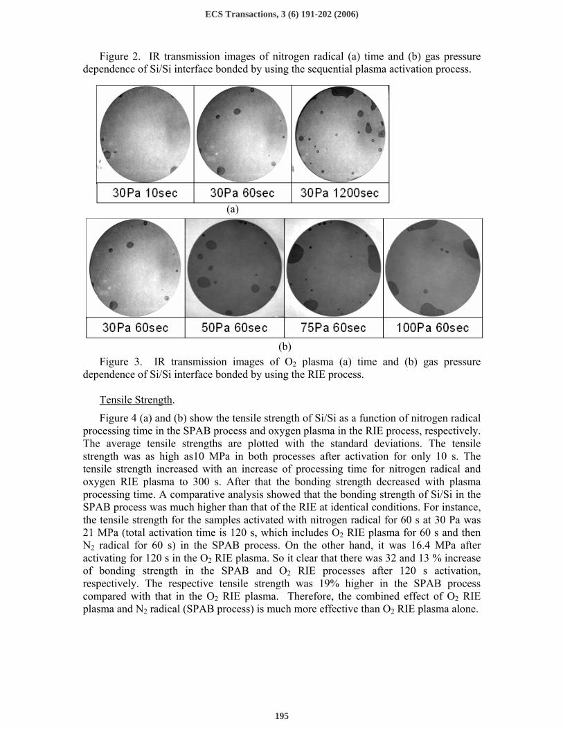
Figure 4 (a) and (b) show the tensile strength of Si/Si as a function of nitrogen radical processing time in the SPAB process and oxygen plasma in the RIE process, respectively. The average tensile strengths are plotted with the standard deviations. The tensile strength was as high as10 MPa in both processes after activation for only 10 s. The tensile strength increased with an increase of processing time for nitrogen radical and oxygen RIE plasma to 300 s. After that the bonding strength decreased with plasma processing time. A comparative analysis showed that the bonding strength of Si/Si in the SPAB process was much higher than that of the RIE at identical conditions. For instance, the tensile strength for the samples activated with nitrogen radical for 60 s at 30 Pa was 21 MPa (total activation time is 120 s, which includes O2 RIE plasma for 60 s and then N2 radical for 60 s) in the SPAB process. On the other hand, it was 16.4 MPa after activating for 120 s in the O2 RIE plasma. So it clear that there was 32 and 13 % increase of bonding strength in the SPAB and O2 RIE processes after 120 s activation, respectively. The respective tensile strength was 19% higher in the SPAB process compared with that in the O2 RIE plasma. Therefore, the combined effect of O2 RIE plasma and N2 radical (SPAB process) is much more effective than O2 RIE plasma alone.
(b)
ECS Transactions, 3 (6) 191-202 (2006)
196
Figure 4. Tensile strength dependence of (a) nitrogen MW radical time in the SPAB process, and (b) oxygen plasma time in the RIE process. In the SPAB process, the oxygen plasma was kept constant for 60 s at 30 Pa. In the O2 RIE plasma, the O2 gas pressure was kept constant at 30 Pa.
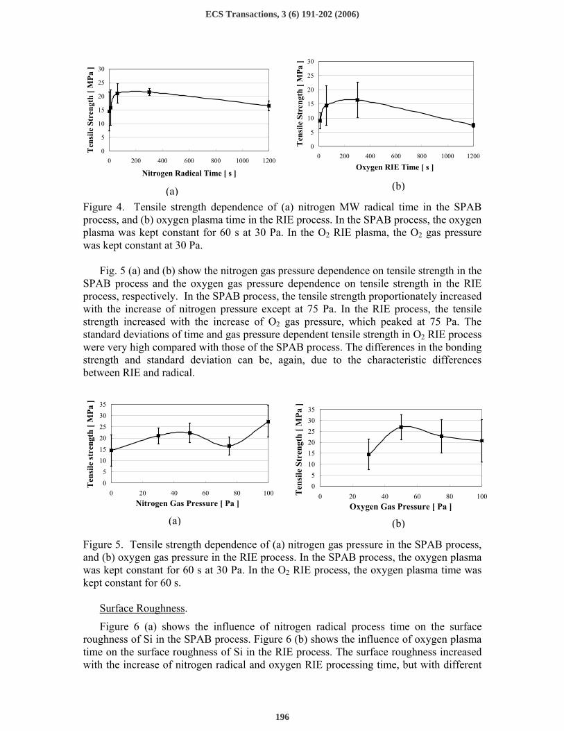
Fig. 5 (a) and (b) show the nitrogen gas pressure dependence on tensile strength in the
SPAB process and the oxygen gas pressure dependence on tensile strength in the RIE process, respectively. In the SPAB process, the tensile strength proportionately increased with the increase of nitrogen pressure except at 75 Pa. In the RIE process, the tensile strength increased with the increase of O2 gas pressure, which peaked at 75 Pa. The standard deviations of time and gas pressure dependent tensile strength in O2 RIE process were very high compared with those of the SPAB process. The differences in the bonding strength and standard deviation can be, again, due to the characteristic differences between RIE and radical.
Figure 5. Tensile strength dependence of (a) nitrogen gas pressure in the SPAB process, and (b) oxygen gas pressure in the RIE process. In the SPAB process, the oxygen plasma was kept constant for 60 s at 30 Pa. In the O2 RIE process, the oxygen plasma time was kept constant for 60 s.
Surface Roughness.
Figure 6 (a) shows the influence of nitrogen radical process time on the surface roughness of Si in the SPAB process. Figure 6 (b) shows the influence of oxygen plasma time on the surface roughness of Si in the RIE process. The surface roughness increased with the increase of nitrogen radical and oxygen RIE processing time, but with different
0
5
10
15
20
25
30
0 200 400 600 800 1000 1200
Nitrogen Radical Time [ s ]
Ten
sile
Str
engt
h [ M
Pa ]
0
5
10
15
20
25
30
35
0 20 40 60 80 100Nitrogen Gas Pressure [ Pa ]
Ten
sile
stre
ngth
[ M
Pa ]
05
101520253035
0 20 40 60 80 100Oxygen Gas Pressure [ Pa ]
Ten
sile
Str
engt
h [ M
Pa ]
0
5
10
15
20
25
30
0 200 400 600 800 1000 1200
Oxygen RIE Time [ s ]
Ten
sile
Str
engt
h [ M
Pa ]
(b)
(a) (b)
(a)
ECS Transactions, 3 (6) 191-202 (2006)
197
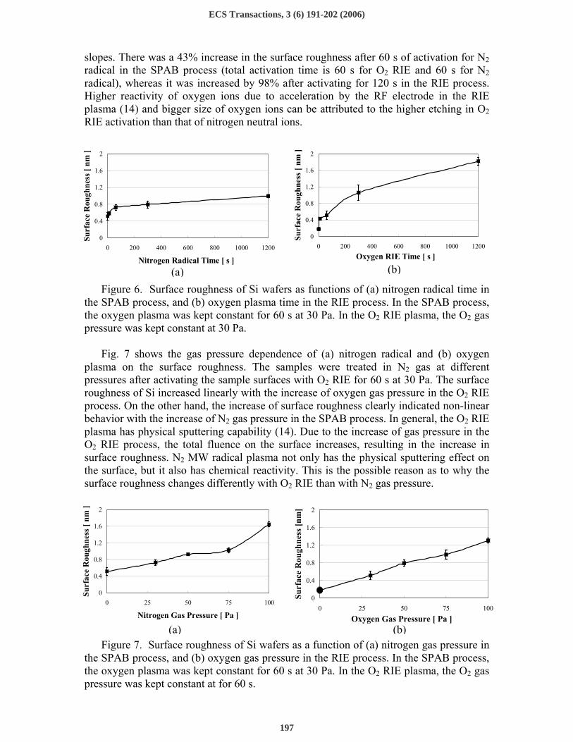
slopes. There was a 43% increase in the surface roughness after 60 s of activation for N2 radical in the SPAB process (total activation time is 60 s for O2 RIE and 60 s for N2 radical), whereas it was increased by 98% after activating for 120 s in the RIE process. Higher reactivity of oxygen ions due to acceleration by the RF electrode in the RIE plasma (14) and bigger size of oxygen ions can be attributed to the higher etching in O2 RIE activation than that of nitrogen neutral ions.
Figure 6. Surface roughness of Si wafers as functions of (a) nitrogen radical time in
the SPAB process, and (b) oxygen plasma time in the RIE process. In the SPAB process, the oxygen plasma was kept constant for 60 s at 30 Pa. In the O2 RIE plasma, the O2 gas pressure was kept constant at 30 Pa.
Fig. 7 shows the gas pressure dependence of (a) nitrogen radical and (b) oxygen
plasma on the surface roughness. The samples were treated in N2 gas at different pressures after activating the sample surfaces with O2 RIE for 60 s at 30 Pa. The surface roughness of Si increased linearly with the increase of oxygen gas pressure in the O2 RIE process. On the other hand, the increase of surface roughness clearly indicated non-linear behavior with the increase of N2 gas pressure in the SPAB process. In general, the O2 RIE plasma has physical sputtering capability (14). Due to the increase of gas pressure in the O2 RIE process, the total fluence on the surface increases, resulting in the increase in surface roughness. N2 MW radical plasma not only has the physical sputtering effect on the surface, but it also has chemical reactivity. This is the possible reason as to why the surface roughness changes differently with O2 RIE than with N2 gas pressure.
Figure 7. Surface roughness of Si wafers as a function of (a) nitrogen gas pressure in
the SPAB process, and (b) oxygen gas pressure in the RIE process. In the SPAB process, the oxygen plasma was kept constant for 60 s at 30 Pa. In the O2 RIE plasma, the O2 gas pressure was kept constant at for 60 s.
0
0.4
0.8
1.2
1.6
2
0 200 400 600 800 1000 1200Oxygen RIE Time [ s ]
Surf
ace
Rou
ghne
ss [
nm ]
0
0.4
0.8
1.2
1.6
2
0 25 50 75 100
Nitrogen Gas Pressure [ Pa ]
Surf
ace
Rou
ghne
ss [
nm ]
0
0.4
0.8
1.2
1.6
2
0 25 50 75 100Oxygen Gas Pressure [ Pa ]
Surf
ace
Rou
ghne
ss [n
m]
0
0.4
0.8
1.2
1.6
2
0 200 400 600 800 1000 1200
Nitrogen Radical Time [ s ]
Surf
ace
Rou
ghne
ss [
nm ]
(a) (b)
(b) (a)
ECS Transactions, 3 (6) 191-202 (2006)

198
A considerable change in the surface roughness was observed right after starting O2 RIE and N2 MW radical processing, as shown in Fig. 6(a) and (b). This can be explained in the following way. While starting plasma and radical processing, the reactions at the near surface compared with to that of the far surface inside the silicon bulk are most likely be different. At the near surface, it is feasible that the formation and structure of materials is unstable, leading to an abrupt change in the surface roughness after plasma and radical processing. At the far surface, the formation and structure are stable resulting in stable reactions (15). Therefore the surface layers of silicon at near surface control the surface activation, whereas the internal layers far from top surface do not have influence on surface activation. The surface roughness increases after prolonged plasma and radical processing. The surface activation increases up to a certain time and regime, then saturates and finally varies as a logarithmic function. Subsequently the surface roughness gradually increases, which lowers the bonding strength and the bonding quality at the interface.
Microstructural Observation.
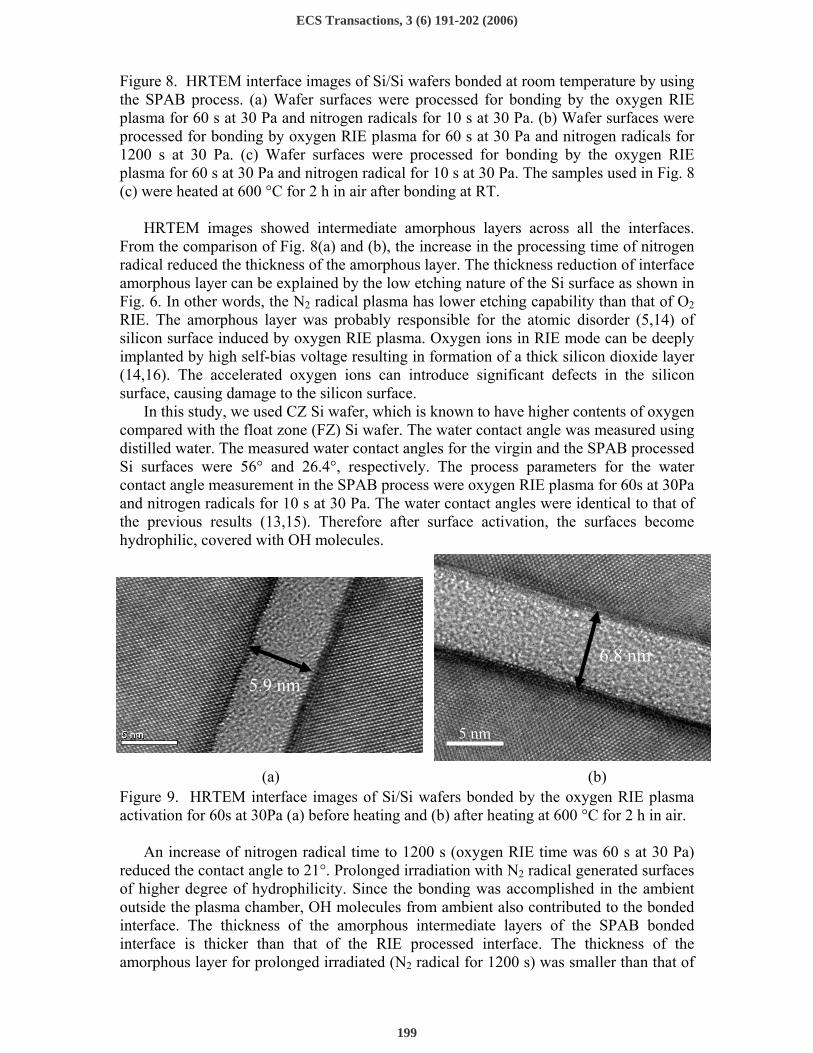
Figure 8(a), and (b) show N2 MW radical processing time influence of SPAB process on the interface images of Si/Si bonded wafers. JEOL 2010 was used for the observation. The bonding conditions for the samples used for Fig. 8(a) were oxygen RIE plasma time 60 s at 30 Pa and nitrogen radical time 10 s at 30 Pa. The bonding conditions for the samples used for Fig. 8 (b) were oxygen RIE plasma time 60 s and nitrogen radical time 1200 s at 30 Pa. Figure 8 (c) shows the HRTEM image of Si/Si interface after heating of the bonded samples being used for figure 8(a). The heating temperature was 600°C for 2 h in air.
5 nm
7.3 nm
9.8 nm
5 nm
8.7 nm
(a) (b)
(c)
ECS Transactions, 3 (6) 191-202 (2006)
199
Figure 8. HRTEM interface images of Si/Si wafers bonded at room temperature by using the SPAB process. (a) Wafer surfaces were processed for bonding by the oxygen RIE plasma for 60 s at 30 Pa and nitrogen radicals for 10 s at 30 Pa. (b) Wafer surfaces were processed for bonding by oxygen RIE plasma for 60 s at 30 Pa and nitrogen radicals for 1200 s at 30 Pa. (c) Wafer surfaces were processed for bonding by the oxygen RIE plasma for 60 s at 30 Pa and nitrogen radical for 10 s at 30 Pa. The samples used in Fig. 8 (c) were heated at 600 °C for 2 h in air after bonding at RT.
HRTEM images showed intermediate amorphous layers across all the interfaces. From the comparison of Fig. 8(a) and (b), the increase in the processing time of nitrogen radical reduced the thickness of the amorphous layer. The thickness reduction of interface amorphous layer can be explained by the low etching nature of the Si surface as shown in Fig. 6. In other words, the N2 radical plasma has lower etching capability than that of O2 RIE. The amorphous layer was probably responsible for the atomic disorder (5,14) of silicon surface induced by oxygen RIE plasma. Oxygen ions in RIE mode can be deeply implanted by high self-bias voltage resulting in formation of a thick silicon dioxide layer (14,16). The accelerated oxygen ions can introduce significant defects in the silicon surface, causing damage to the silicon surface.
In this study, we used CZ Si wafer, which is known to have higher contents of oxygen compared with the float zone (FZ) Si wafer. The water contact angle was measured using distilled water. The measured water contact angles for the virgin and the SPAB processed Si surfaces were 56° and 26.4°, respectively. The process parameters for the water contact angle measurement in the SPAB process were oxygen RIE plasma for 60s at 30Pa and nitrogen radicals for 10 s at 30 Pa. The water contact angles were identical to that of the previous results (13,15). Therefore after surface activation, the surfaces become hydrophilic, covered with OH molecules.
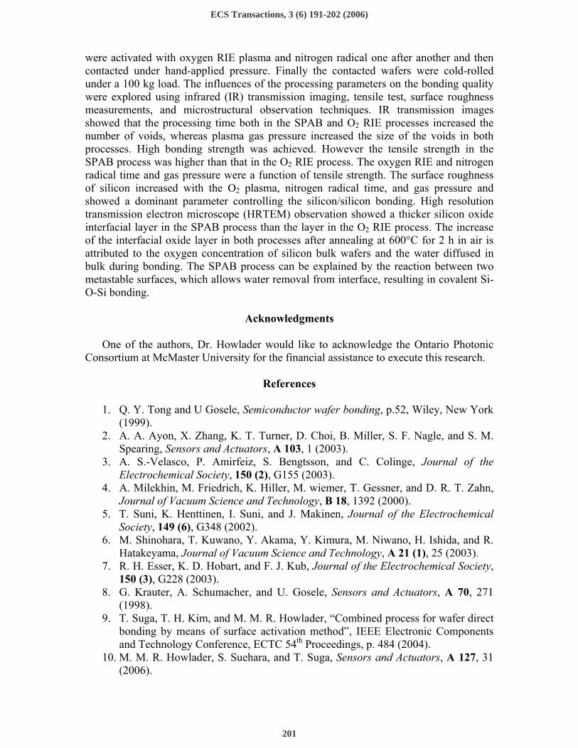
Figure 9. HRTEM interface images of Si/Si wafers bonded by the oxygen RIE plasma activation for 60s at 30Pa (a) before heating and (b) after heating at 600 °C for 2 h in air.
An increase of nitrogen radical time to 1200 s (oxygen RIE time was 60 s at 30 Pa)
reduced the contact angle to 21°. Prolonged irradiation with N2 radical generated surfaces of higher degree of hydrophilicity. Since the bonding was accomplished in the ambient outside the plasma chamber, OH molecules from ambient also contributed to the bonded interface. The thickness of the amorphous intermediate layers of the SPAB bonded interface is thicker than that of the RIE processed interface. The thickness of the amorphous layer for prolonged irradiated (N2 radical for 1200 s) was smaller than that of
5 nm
6.8 nm 5.9 nm
(a) (b)
ECS Transactions, 3 (6) 191-202 (2006)

200
the shorter irradiated (N2 radical for 10 s) sample. Prolonged irradiation with N2 radical after O2 RIE plasma may lead chemical reactions, which have a dominant effect, to increase porosity in the amorphous layer. This is in agreement with the surface porosity in Si surface induced by O2 plasma (5,15,17). The porous layers accommodate OH groups (5) and have increased water diffusivity (14). The presence of these layers can be attributed to the shrinkage of amorphous layers. Further investigation with electron energy loss spectroscopy is planned to gain insight in order to clarify the role of N2 radical on the interfacial amorphous layer.
Figure 9(a) and (b) show the HRTEM interface images of Si/Si wafers bonded by the oxygen RIE plasma activation for 60 s at 30 Pa before heating and after heating at 600°C for 2 h in air, respectively. If we compare figures 8(a) and 9(a), we can see that there are amorphous oxide layers across the interfaces. Since the native oxide of Si is about 1 nm (16), the increase in oxide thickness across the interface by 6-8 times is indicative of oxidation induced by O2 RIE and nitrogen radical. Further comparison indicated lower contribution of sequential activation on oxide thickness than of O2 RIE. The heating influence on the amorphous layer across the interface can clearly be seen in SPAB (compare 8(a) and 8(c)) and O2 RIE plasma (compare 9(a) and 9(b)) processes. The thickness of the amorphous layers increased by about 1 nm in both processes after heating at 600 °C for 2 h. As mentioned previously, the silicon wafers used in this work were CZ type, which has relatively high oxygen content. The oxygen concentration in silicon bulk wafers moves toward interface after getting thermal energy and diffuses into the amorphous layer, thereby increases the thickness of the amorphous layer after heating. Consistent results of a thickening interfacial oxide layer in CZ bonded wafers after annealing have been reported (19). In addition, the water diffused in the bulk of silicon wafers during chemical reactions in O2 RIE and nitrogen radical dissociates into OH and H, and contributes to the amorphous layer.
Bonding Mechanism
The bonding mechanism of the SPAB process is similar to that of the hydrophilic bonding process. The only difference between the SPAB and hydrophilic processes is that in the SPAB process, the surfaces are activated in such a way so that no heating is required to enhance the bonding strength. Without heating, the spontaneous reactions between the sequential activated surfaces resulted in strong bonding. As previously mentioned, the SPAB process is a two step activation process. In the first step, O2 RIE plasma removes the native oxide of Si surface by physical sputtering and generates oxides on silicon surface. In the second step, nitrogen radical produces thermodynamically and chemically unstable surfaces, which probably contain oxygen and nitrogen. The metastable surfaces become more hydrophilic after sequential activation, which is justified by the decrease of the water contact angle at that condition. The activated surfaces are also believed to have increased porosity. When metastable surfaces are contacted in atmospheric air with moderate humidity, OH molecules from the air that stick to the surfaces react with hydrogen, producing water. The water diffuses in porous silicon oxynitride layers and resulted in covalent bonding of Si-O-Si.
Conclusions
Sequential plasma activation (SPAB) process utilizing the physical sputtering of oxygen reactive ion etching (RIE) and the chemical reactivity of nitrogen microwave (MW) radical was developed for room-temperature silicon direct bonding (SDB). The wafers
ECS Transactions, 3 (6) 191-202 (2006)
201
were activated with oxygen RIE plasma and nitrogen radical one after another and then contacted under hand-applied pressure. Finally the contacted wafers were cold-rolled under a 100 kg load. The influences of the processing parameters on the bonding quality were explored using infrared (IR) transmission imaging, tensile test, surface roughness measurements, and microstructural observation techniques. IR transmission images showed that the processing time both in the SPAB and O2 RIE processes increased the number of voids, whereas plasma gas pressure increased the size of the voids in both processes. High bonding strength was achieved. However the tensile strength in the SPAB process was higher than that in the O2 RIE process. The oxygen RIE and nitrogen radical time and gas pressure were a function of tensile strength. The surface roughness of silicon increased with the O2 plasma, nitrogen radical time, and gas pressure and showed a dominant parameter controlling the silicon/silicon bonding. High resolution transmission electron microscope (HRTEM) observation showed a thicker silicon oxide interfacial layer in the SPAB process than the layer in the O2 RIE process. The increase of the interfacial oxide layer in both processes after annealing at 600°C for 2 h in air is attributed to the oxygen concentration of silicon bulk wafers and the water diffused in bulk during bonding. The SPAB process can be explained by the reaction between two metastable surfaces, which allows water removal from interface, resulting in covalent Si-O-Si bonding.
Acknowledgments
One of the authors, Dr. Howlader would like to acknowledge the Ontario Photonic Consortium at McMaster University for the financial assistance to execute this research.
References
1. Q. Y. Tong and U Gosele, Semiconductor wafer bonding, p.52, Wiley, New York
(1999). 2. A. A. Ayon, X. Zhang, K. T. Turner, D. Choi, B. Miller, S. F. Nagle, and S. M.
Spearing, Sensors and Actuators, A 103, 1 (2003). 3. A. S.-Velasco, P. Amirfeiz, S. Bengtsson, and C. Colinge, Journal of the
Electrochemical Society, 150 (2), G155 (2003). 4. A. Milekhin, M. Friedrich, K. Hiller, M. wiemer, T. Gessner, and D. R. T. Zahn,
Journal of Vacuum Science and Technology, B 18, 1392 (2000). 5. T. Suni, K. Henttinen, I. Suni, and J. Makinen, Journal of the Electrochemical
Society, 149 (6), G348 (2002). 6. M. Shinohara, T. Kuwano, Y. Akama, Y. Kimura, M. Niwano, H. Ishida, and R.
Hatakeyama, Journal of Vacuum Science and Technology, A 21 (1), 25 (2003). 7. R. H. Esser, K. D. Hobart, and F. J. Kub, Journal of the Electrochemical Society,
150 (3), G228 (2003). 8. G. Krauter, A. Schumacher, and U. Gosele, Sensors and Actuators, A 70, 271
(1998). 9. T. Suga, T. H. Kim, and M. M. R. Howlader, “Combined process for wafer direct
bonding by means of surface activation method”, IEEE Electronic Components and Technology Conference, ECTC 54th Proceedings, p. 484 (2004).
10. M. M. R. Howlader, S. Suehara, and T. Suga, Sensors and Actuators, A 127, 31 (2006).
ECS Transactions, 3 (6) 191-202 (2006)

202
11. M. M. R. Howlader, S. Suehara, H. Takagi, T. H. Kim, R. Maeda, and T. Suga, IEEE Adv. Packag, 30(1), (2006).
12. X. X. Zhang and J.-P. Raskin, Journal of Microelectromechanical Systems, 140 (2), 368 (2005).
13. M. Wiegand, M. Reiche, and U. Gösele, Journal of the Electrochemical Society, 147 (7), 2734 (2000).
14. D. Pasquariello, C. Hedlund, and K. Hjort, Journal of the Electrochemical Society, 147 (7), 2699 (2000).
15. K. S.-Henriksen, M. M. V. Taklo, A. Hanneborg, and G. U. Jensen, Sensors and Actuators, A 102, 99 (2002).
16. M. M. Visser, S. Weichel, R. de Reus, and A. B. Hanneborg, Sensors and Actuators, A 97-98, 434 (2002).
17. A. Weinert, P. Amirfeiz, and S. Bengtsson, Sensors and Actuators, A 92, 214 (2001).
18. D. Resnik, D. Vrtacnik, U. Aljancic, S. Amon, Sensors and Actuators, A 80, 68 (2000).
19. K.-Y. Ahn, R. Stengl, T. Y. Tan, U. Gosele, and P. Smith, Appl. Phys. A 50, 85 (1990).
ECS Transactions, 3 (6) 191-202 (2006)