serial ata international organization: serial ata ... · serial ata international organization:...
TRANSCRIPT
Serial ATA International Organization:
Serial ATA Interoperability Program Revision 1.4.3 Unified Test Document Version 1.01
May 29, 2012
SATA-IO Board Members:
Dell Computer Corporation Hewlett Packard Corporation
Hitachi Global Storage Technologies, Inc. Intel Corporation
Marvell Semiconductor, Inc. PMC-Sierra, Inc.
SanDisk Seagate Technology
Western Digital Corporation
2
Serial ATA International Organization: Serial ATA Interoperability Program Unified Test Document is available for download at http://www.sata-io.org.
DOCUMENT DISCLAIMER THIS DOCUMENT IS PROVIDED TO YOU “AS IS” WITH NO WARRANTIES WHATSOEVER, INCLUDING ANY WARRANTY OF MERCHANTABILITY, NON-INFRINGEMENT, OR FITNESS FOR ANY PARTICULAR PURPOSE. THE AUTHORS OF THIS DOCUMENT DISCLAIM ALL LIABILITY, INCLUDING LIABILITY FOR INFRINGEMENT OF ANY PROPRIETARY RIGHTS, RELATING TO USE OR IMPLEMENTATION OF INFORMATION IN THIS DOCUMENT. THE AUTHORS DO NOT WARRANT OR REPRESENT THAT SUCH USE WILL NOT INFRINGE SUCH RIGHTS. THE PROVISION OF THIS DOCUMENT TO YOU DOES NOT PROVIDE YOU WITH ANY LICENSE, EXPRESS OR IMPLIED, BY ESTOPPEL OR OTHERWISE, TO ANY INTELLECTUAL PROPERTY RIGHTS. Copyright 2002-2011, Serial ATA International Organization. All rights reserved. For more information about Serial ATA, refer to the Serial ATA International Organization website at http://www.sata-io.org. All product names are trademarks, registered trademarks, or servicemarks of their respective owners. All test procedures and techniques outlined in this UTD shallbe free of restriction necessary for implementation and shallobserve absolute IP neutrality. Should a member identify any section of this document which references or suggests test methodology which is restricted, it should be brought to the attention to the Logo committee and reviewed with the intent of removal from this document. Serial ATA International Organization contact information:
SATA-IO 3855 SW 158th Drive Beaverton Oregon 97006 USA Tel: +1 (503) 619-0572 Fax: +1 503-644-6708 E-mail: mailto:[email protected]
3
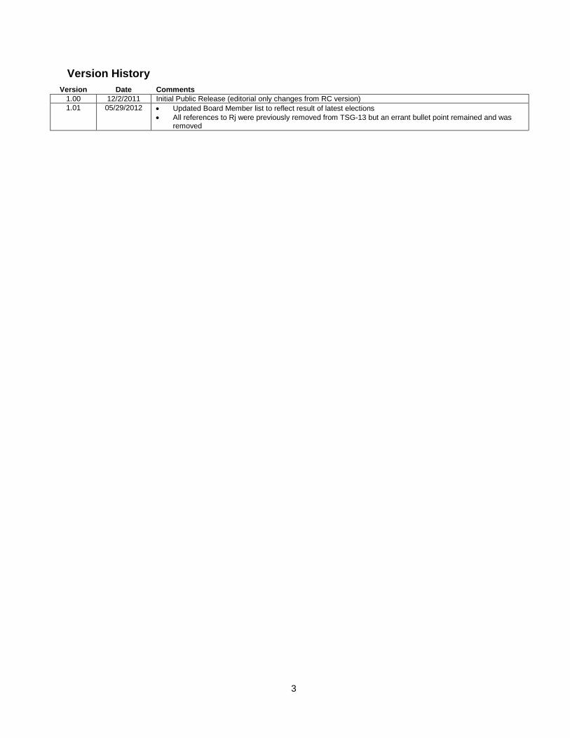
Version History Version Date Comments
1.00 12/2/2011 Initial Public Release (editorial only changes from RC version) 1.01 05/29/2012 • Updated Board Member list to reflect result of latest elections
• All references to Rj were previously removed from TSG-13 but an errant bullet point remained and was removed
4
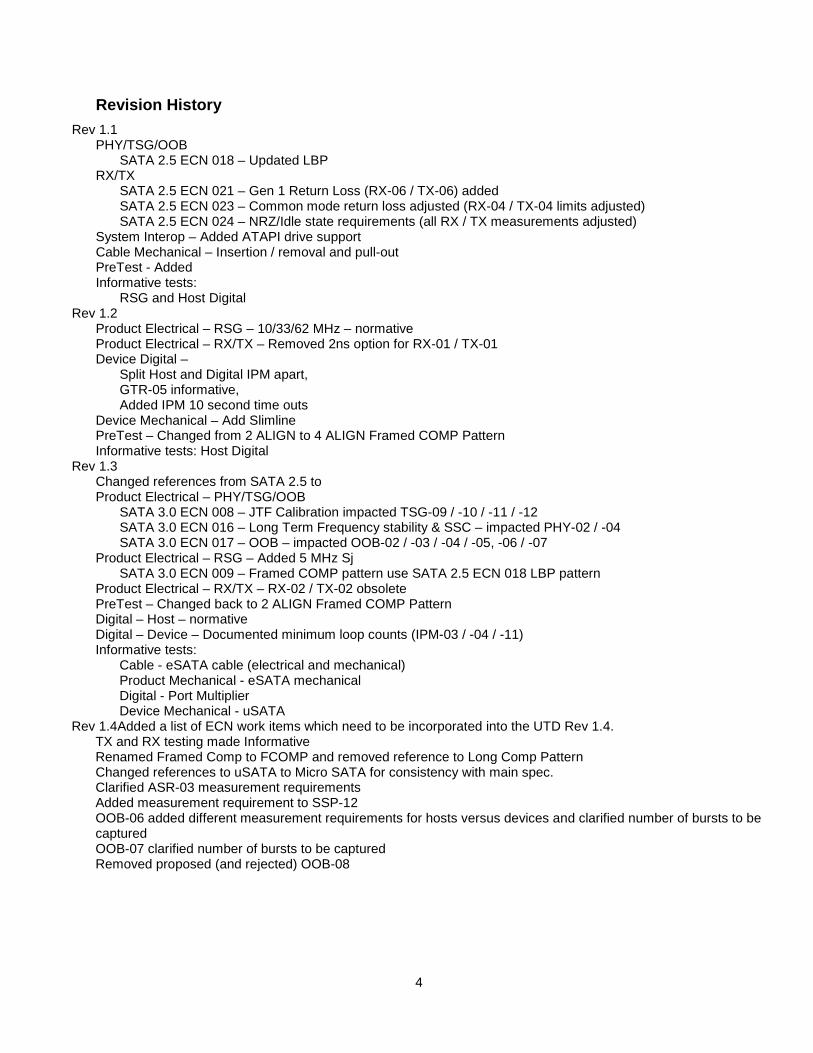
Revision History Rev 1.1
PHY/TSG/OOB SATA 2.5 ECN 018 – Updated LBP
RX/TX SATA 2.5 ECN 021 – Gen 1 Return Loss (RX-06 / TX-06) added SATA 2.5 ECN 023 – Common mode return loss adjusted (RX-04 / TX-04 limits adjusted) SATA 2.5 ECN 024 – NRZ/Idle state requirements (all RX / TX measurements adjusted)
System Interop – Added ATAPI drive support Cable Mechanical – Insertion / removal and pull-out PreTest - Added Informative tests:
RSG and Host Digital Rev 1.2
Product Electrical – RSG – 10/33/62 MHz – normative Product Electrical – RX/TX – Removed 2ns option for RX-01 / TX-01 Device Digital –
Split Host and Digital IPM apart, GTR-05 informative, Added IPM 10 second time outs
Device Mechanical – Add Slimline PreTest – Changed from 2 ALIGN to 4 ALIGN Framed COMP Pattern Informative tests: Host Digital
Rev 1.3 Changed references from SATA 2.5 to Product Electrical – PHY/TSG/OOB
SATA 3.0 ECN 008 – JTF Calibration impacted TSG-09 / -10 / -11 / -12 SATA 3.0 ECN 016 – Long Term Frequency stability & SSC – impacted PHY-02 / -04 SATA 3.0 ECN 017 – OOB – impacted OOB-02 / -03 / -04 / -05, -06 / -07
Product Electrical – RSG – Added 5 MHz Sj SATA 3.0 ECN 009 – Framed COMP pattern use SATA 2.5 ECN 018 LBP pattern
Product Electrical – RX/TX – RX-02 / TX-02 obsolete PreTest – Changed back to 2 ALIGN Framed COMP Pattern Digital – Host – normative Digital – Device – Documented minimum loop counts (IPM-03 / -04 / -11) Informative tests:
Cable - eSATA cable (electrical and mechanical) Product Mechanical - eSATA mechanical Digital - Port Multiplier Device Mechanical - uSATA
Rev 1.4Added a list of ECN work items which need to be incorporated into the UTD Rev 1.4. TX and RX testing made Informative Renamed Framed Comp to FCOMP and removed reference to Long Comp Pattern Changed references to uSATA to Micro SATA for consistency with main spec. Clarified ASR-03 measurement requirements Added measurement requirement to SSP-12 OOB-06 added different measurement requirements for hosts versus devices and clarified number of bursts to be captured OOB-07 clarified number of bursts to be captured Removed proposed (and rejected) OOB-08
5
Table of Contents 1. Goals, Objectives, & Constraints............................................................................................................................... 9
1.1. References ......................................................................................................................................................... 9 1.1.1. Definitions ................................................................................................................................................. 11 1.1.2. Conventions .............................................................................................................................................. 12
1.2. Product Classes ............................................................................................................................................... 13 1.2.1. Expected Behavior .................................................................................................................................... 13 1.2.2. Measurement Requirements .................................................................................................................... 13 1.2.3. Pass/Fail Criteria ....................................................................................................................................... 13
1.3. Methods of Implementation .............................................................................................................................. 13 1.4. Test Product Considerations ............................................................................................................................ 14
1.4.1. Common Host/Device/Port Multiplier BIST Considerations ...................................................................... 14 1.4.2. Device specific considerations .................................................................................................................. 14 1.4.3. Cable Considerations ................................................................................................................................ 14 1.4.4. Host Considerations .................................................................................................................................. 14 1.4.5. Port Multiplier Considerations ................................................................................................................... 15
2. Interoperability Specification Test Summary ........................................................................................................... 15 2.1. General Test Requirements ............................................................................................................................. 18
2.1.1. GTR-01 – Software Reset......................................................................................................................... 18 2.1.2. GTR-02 – SATA Gen-2 or above Signaling Speed Backwards Compatibility .......................................... 18 2.1.3. GTR-03 – DMA Protocol Support ............................................................................................................. 19 2.1.4. GTR-04 – General SATA Support ............................................................................................................ 20 2.1.5. GTR-05 : Unrecognized FIS receipt (Informative) .................................................................................... 21
2.2. Native Command Queuing ............................................................................................................................... 21 2.2.1. NCQ-01 : Forced Unit Access................................................................................................................... 21 2.2.2. NCQ-02 : Read Log Ext log page 10h support ......................................................................................... 22 2.2.3. NCQ-03 : Intermix of Legacy and NCQ commands ................................................................................. 22 2.2.4. NCQ-04 : Device response to malformed NCQ command ....................................................................... 23 2.2.5. NCQ-05 : DMA Setup Auto-Activate ......................................................................................................... 25
2.3. Asynchronous Signal Recovery ....................................................................................................................... 25 2.3.1. ASR-01 : COMINIT response interval ....................................................................................................... 25 2.3.2. ASR-02 : COMINIT OOB Interval ............................................................................................................. 26 2.3.3. ASR-03 : COMRESET OOB Interval ........................................................................................................ 26
2.4. Software Settings Preservation ........................................................................................................................ 26 2.4.1. SSP-01 : Initialize Device Parameters ...................................................................................................... 27 2.4.2. SSP-02 : Read/Write Stream Error Log .................................................................................................... 27 2.4.3. SSP-03 : Security Mode State .................................................................................................................. 28 2.4.4. SSP-04 : Set Address Max ....................................................................................................................... 28 2.4.5. SSP-05 : Set Features – Write Cache Enable/Disable ............................................................................. 29 2.4.6. SSP-06 : Set Features – Set Transfer Mode ............................................................................................ 30 2.4.7. SSP-07 : Set Features – Advanced Power Management Enable/Disable ............................................... 30 2.4.8. SSP-08 : Set Features – Read Look-Ahead ............................................................................................. 31 2.4.9. SSP-09 : Set Features – Release Interrupt .............................................................................................. 31 2.4.10. SSP-10 : Set Features – Service Interrupt ............................................................................................ 32 2.4.11. SSP-11 : Set Multiple Mode (Informative) ............................................................................................. 32 2.4.12. SSP-12 : Set Features – Write-Read-Verify.......................................................................................... 33
2.5. Interface Power Management .......................................................................................................................... 33 2.5.1. IPM-01 : Partial State exit latency (host-initiated) ..................................................................................... 34 2.5.2. IPM-02 : Slumber State exit latency (host-initiated) ................................................................................. 34 2.5.3. IPM-03 : Speed matching upon resume (host-initiated) ........................................................................... 35 2.5.4. IPM-04 : NAK of requests when support not indicated ............................................................................. 36 2.5.5. IPM-05 : Response to PMREQ_P ............................................................................................................ 37 2.5.6. IPM-06 : Response to PMREQ_S ............................................................................................................ 37 2.5.7. IPM-07 : Device default setting for device initiated requests .................................................................... 38 2.5.8. IPM-08 : Device Initiated Power Management enable / disable ............................................................... 38
6
2.5.9. IPM-09 : Partial State exit latency (device-initiated) ................................................................................. 39 2.5.10. IPM-10 : Slumber State exit latency (device-initiated) .......................................................................... 40 2.5.11. IPM-11 : Speed matching upon resume (device-initiated) .................................................................... 41
2.6. Digital Optional Features .................................................................................................................................. 42 2.6.1. DOF-01 : Asynchronous notification ......................................................................................................... 42 2.6.2. DOF-02 : Phy speed indicator .................................................................................................................. 43
2.7. Mechanical - Cable Assembly - Standard Internal and eSATA ....................................................................... 43 2.7.1. MCI-01 : Visual and Dimensional Inspections .......................................................................................... 44 2.7.2. MCI-02 : Insertion Force (Latching and Non-Latching) ............................................................................ 44 2.7.3. MCI-03 : Removal Force (Non-Latching) .................................................................................................. 45 2.7.4. MCI-04 : Removal Force (Latching) .......................................................................................................... 45 2.7.5. MCX-05 : Cable Pull-out - internal (normative) and eSATA (informative) cables ..................................... 45 2.7.6. MCE-01 : Visual and Dimension Inspection for eSATA cables (informative) ........................................... 45
2.8. Electrical - Cable Assembly – Standard Internal and eSATA .......................................................................... 46 2.8.1. SI-01 : Mated Connector Impedance ........................................................................................................ 46 2.8.2. SI-02 : Cable Absolute Impedance ........................................................................................................... 47 2.8.3. SI-03 : Cable Pair Matching ...................................................................................................................... 47 2.8.4. SI-04 : Common Mode Impedance ........................................................................................................... 48 2.8.5. SI-05 : Differential Rise Time .................................................................................................................... 49 2.8.6. SI-06 : Intra-Pair Skew .............................................................................................................................. 49 2.8.7. SI-07 : Insertion Loss ................................................................................................................................ 49 2.8.8. SI-08 : Differential to Differential Crosstalk: NEXT ................................................................................... 50 2.8.9. SI-09 : Inter-Symbol Interference .............................................................................................................. 50
2.9. Mechanical – Device - Standard Internal Connector ....................................................................................... 51 2.9.1. MDI-01 : Connector Location .................................................................................................................... 51 2.9.2. MDI-02 : Visual and Dimensional Inspections .......................................................................................... 53
2.10. Mechanical – Device - Power Connector ..................................................................................................... 54 2.10.1. MDP-01 : Visual and Dimensional Inspections ..................................................................................... 54
2.11. Mechanical – Host - Standard Internal Connector ....................................................................................... 54 2.11.1. MHI-01 : Visual and Dimensional Inspections (Informative) ................................................................. 54
2.12. Mechanical – Drive/Host – eSATA Connector (informative) ........................................................................ 55 2.12.1. MXE-01 : Visual and Dimension Inspection .......................................................................................... 55
2.13. Phy General Requirements .......................................................................................................................... 56 2.13.1. PHY-01 : Unit Interval ............................................................................................................................ 56 2.13.2. PHY-02 : Frequency Long Term Stability .............................................................................................. 56 2.13.3. PHY-03 : Spread-Spectrum Modulation Frequency .............................................................................. 56 2.13.4. PHY-04 : Spread-Spectrum Modulation Deviation ................................................................................ 57
2.14. Phy Transmitter Requirements ..................................................................................................................... 57 2.14.1. TX-01 : Pair Differential Impedance(Informative) .................................................................................. 57 2.14.2. TX-02 : Single-Ended Impedance (Obsolete) ....................................................................................... 57 2.14.3. TX-03 : Gen2 (3 Gbps) Differential Mode Return Loss (Informative) ................................................... 58 2.14.4. TX-04 : Gen2 (3 Gbps) Common Mode Return Loss (Informative) ...................................................... 58 2.14.5. TX-05 : Gen2 (3 Gbps) Impedance Balance (Informative) ................................................................... 59 2.14.6. TX-06 : Gen1 (1.5 Gbps) Differential Mode Return Loss (Informative) ................................................ 60 2.14.7. TX-07 : Gen3 (6 Gbps) Differential Mode Return Loss (Informative) ................................................... 60 2.14.8. TX-08 : Gen3 (6 Gbps) Impedance Balance (Informative) ................................................................... 61
2.15. Phy Transmit Signal Requirements .............................................................................................................. 62 2.15.1. TSG-01 : Differential Output Voltage .................................................................................................... 62 2.15.2. TSG-02 : Rise/Fall Time (Informative) .................................................................................................. 63 2.15.3. TSG-03 : Differential Skew (Informative) .............................................................................................. 64 2.15.4. TSG-04 : AC Common Mode Voltage ................................................................................................... 64 2.15.5. TSG-05 : Rise/Fall Imbalance (Obsolete) ............................................................................................. 65 2.15.6. TSG-06 : Amplitude Imbalance (Obsolete) ........................................................................................... 65 2.15.7. TSG-07 : Gen1 (1.5 Gbps) TJ at Connector, Clock to Data, fBAUD/10 (Obsolete) ................................. 65 2.15.8. TSG-08 : Gen1 (1.5 Gbps) DJ at Connector, Clock to Data, fBAUD/10 (Obsolete) ................................ 65 2.15.9. TSG-09 : Gen1 (1.5 Gbps) TJ at Connector, Clock to Data, fBAUD/500 ................................................. 66
7
2.15.10. TSG-10 : Gen1 (1.5 Gbps) DJ at Connector, Clock to Data, fBAUD/500 ................................................ 66 2.15.11. TSG-11 : Gen2 (3 Gbps) TJ at Connector, Clock to Data, fBAUD/500 .................................................... 67 2.15.12. TSG-12 : Gen2 (3 Gbps) DJ at Connector, Clock to Data, fBAUD/500 ................................................... 67 2.15.13. TSG-13: Gen3 (6 Gbps) Transmit Jitter .............................................................................................. 67 2.15.14. TSG-14 : Gen3 (6 Gbps)TX Maximum Differential Voltage Amplitude ................................................. 68 2.15.15. TSG-15 : Gen3 (6 Gbps) TX Minimum Differential Voltage Amplitude ................................................. 68 2.15.16. TSG-16 : Gen3 (6 Gbps) Tx AC Common Mode Voltage ..................................................................... 69
2.16. Phy Receiver Requirements ......................................................................................................................... 69 2.16.1. RX-01 : Pair Differential Impedance (Informative) ................................................................................ 69 2.16.2. RX-02 : Single-Ended Impedance (Obsolete) ....................................................................................... 70 2.16.3. RX-03 : Gen2 (3 Gbps) Differential Mode Return Loss (Informative) ................................................... 70 2.16.4. RX-04 : Gen2 (3 Gbps) Common Mode Return Loss (Informative) ...................................................... 71 2.16.5. RX-05 : Gen2 (3 Gbps) Impedance Balance(Informative) .................................................................... 71 2.16.6. RX-06 : Gen1 (1.5 Gbps) Differential Mode Return Loss (Informative) ................................................ 72 2.16.7. RX-07 : Gen3 (6 Gbps) Differential Mode Return Loss (Informative) ................................................... 72 2.16.8. RX-08 : Gen3 (6 Gbps) Impedance Balance (Informative) ................................................................... 73
2.17. Phy Receive Signal Requirements ............................................................................................................... 74 2.17.1. General RSG Calibration Requirements ............................................................................................... 74 2.17.2. RSG-01 : Gen1 (1.5 Gbps) Receiver Jitter Tolerance Test .................................................................. 76 2.17.3. RSG-02 : Gen2 (3 Gbps) Receiver Jitter Tolerance Test ..................................................................... 77 2.17.4. RSG-03 : Gen3 (6 Gbps) Receiver Jitter Tolerance Test ..................................................................... 77 2.17.5. RSG-04 : Reserved place holder .......................................................................................................... 78 2.17.6. RSG-05 : Receiver Stress Test at +350 ppm ........................................................................................ 78 2.17.7. RSG-06 : Receiver Stress Test With SSC (Informative) ....................................................................... 78
2.18. Phy OOB Requirements ............................................................................................................................... 78 2.18.1. OOB-01 : OOB Signal Detection Threshold .......................................................................................... 79 2.18.2. OOB-02 : UI During OOB Signaling ...................................................................................................... 79 2.18.3. OOB-03 : COMINIT/RESET and COMWAKE Transmit Burst Length .................................................. 80 2.18.4. OOB-04 : COMINIT/RESET Transmit Gap Length ............................................................................... 80 2.18.5. OOB-05 : COMWAKE Transmit Gap Length ........................................................................................ 80 2.18.6. OOB-06 : COMWAKE Gap Detection Windows ................................................................................... 81 2.18.7. OOB-07 : COMINIT/COMRESET Gap Detection Windows .................................................................. 83
2.19. Port Multiplier Requirements (informative) ................................................................................................... 85 2.19.1. PM-01 : Device Port 0 Enabled by Default............................................................................................ 85 2.19.2. PM-02 : General Status and Control Register (GSCR) Access ............................................................ 86 2.19.3. PM-03 : Port Status and Control Register (PSCR) Access ................................................................... 87 2.19.4. PM-04 : 3 Gbps Backwards Compatibility ............................................................................................. 88 2.19.5. PM-05 : Interface Power Management, H – PM, Host Initiated ............................................................ 88 2.19.6. PM-06 : Interface Power Management, H - PM, PM Initiated ............................................................... 90 2.19.7. PM-07 : Interface Power Management, PM - Dev, PM Initiated ........................................................... 91 2.19.8. PM-08 : Interface Power Management, PM - Dev, Dev Initiated .......................................................... 92 2.19.9. PM-09 : Speed matching upon resume (H-PM interface) ..................................................................... 93 2.19.10. PM-10 : Speed matching upon resume (PM-Dev interface) ................................................................. 95 2.19.11. PM-11 : Port Multiplier Reset Response ............................................................................................... 96 2.19.12. PM-12 : Device Port 0 Hot Plug with non-PM aware host software. ..................................................... 97 2.19.13. PM-13 : Hot Plug with PM aware host software. ................................................................................... 98 2.19.14. PM-14 : FIS Sent To a Disabled Device Port. ....................................................................................... 99 2.19.15. PM-15 : FIS Sent To a Invalid Device Port Address. ............................................................................ 99 2.19.16. PM-16 : Test For PM-aware Host ....................................................................................................... 100
3. System Interoperability Tests ................................................................................................................................ 100 3.1. System Description ........................................................................................................................................ 100
3.1.1. System Product Selection ....................................................................................................................... 101 3.1.2. System Interoperability non-PUT Cable requirements ........................................................................... 101 3.1.3. System Interoperability Host Requirements for Device testing .............................................................. 101 3.1.4. System Interoperability Device Requirements for Host testing .............................................................. 102
3.2. System Interoperability Test Description ....................................................................................................... 102
8
3.2.1. Resource requirements ........................................................................................................................... 103 3.2.2. SYS-01: System Interoperability Test Requirements ............................................................................. 103 3.2.3. System Interop Pass / Fail Criteria ......................................................................................................... 104
3.3. System Interoperability Test Tool Validation requirements ........................................................................... 104 3.3.1. SYT-01 – Data pattern validation ............................................................................................................ 105 3.3.2. SYT-02 – Data pattern alignment ........................................................................................................... 105 3.3.3. SYT-03 – 8 KB Data FIS usage .............................................................................................................. 105 3.3.4. SYT-04 – Data error detection ................................................................................................................ 105 3.3.5. SYT-05 – Complete Data set, including Host caching and retries.......................................................... 106 3.3.6. SYT-06 - Data file signatures .................................................................................................................. 106 3.3.7. SYT-07 - Data Pattern set....................................................................................................................... 106 3.3.8. SYT-08 - Test duration ............................................................................................................................ 106 3.3.9. SYT-09 – System Configuration ............................................................................................................. 106 3.3.10. SYT-10 – OS Install ............................................................................................................................. 107
4. Calibration and Verification of Jitter Measurement Devices (JTF Cal) ................................................................. 107 4.1. SATA 3.0 ECN 009 Long FRAMED COMP Pattern ...................................................................................... 110
9
1. Goals, Objectives, & Constraints This document defines the test requirements specific to the SATA-IO Interoperability Program. Many of the test requirements are associated with a subset of requirements included in Serial ATA Revision 3.1 and these test requirements are based upon the requirements for the Serial ATA protocol and features, intended to verify a subset of the Specification requirements and ensuring compatibility for Serial ATA. Not every feature or capability within the Serial ATA architecture may be included in the Integrator’s List testing. The requirements are driven by the necessary capabilities of the Specification that can be verified by functional testing. There are additional test requirements which are intended to verify general system interoperability which are not associated with any Specification requirements. Some of the goals and requirements for the Interoperability Program documentation include:
• Maintain adherence to Serial ATA Specification(s) across all SATA products • Maintain compatibility with older hosts & devices without compromising product adherence to the
Specification • Deliver standard test requirements for Serial ATA products
1.1. References This document is not a Serial ATA Specification but includes requirements for testing adherence to a subset of the Serial ATA Specification guidelines, in addition to system interoperability tests. This document makes reference to the following Specifications and documents:
• Serial ATA Revision 3.1. Available for download at www.sata-io.org. • AT Attachment with Packet Interface – 6 (ATA/ATAPI-6). Draft available at www.t13.org. Published
ATA/ATAPI Specifications available from ANSI at webstore.ansi.org or from Global Engineering. • Serial ATA Interoperability Program Revision 1.3 Policy Document. Available for download at www.sata-
io.org. • Serial ATA Interoperability Program Revision 1.3 Description Document. Available for download at www.sata-
io.org.
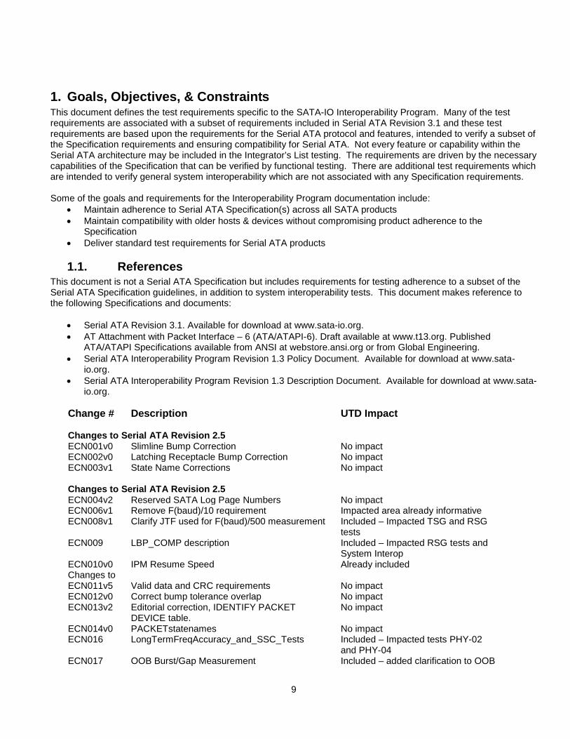
Change # Description UTD Impact Changes to Serial ATA Revision 2.5 ECN001v0 Slimline Bump Correction No impact ECN002v0 Latching Receptacle Bump Correction No impact ECN003v1 State Name Corrections No impact Changes to Serial ATA Revision 2.5 ECN004v2 Reserved SATA Log Page Numbers No impact ECN006v1 Remove F(baud)/10 requirement Impacted area already informative ECN008v1 Clarify JTF used for F(baud)/500 measurement Included – Impacted TSG and RSG
tests ECN009 LBP_COMP description Included – Impacted RSG tests and
System Interop ECN010v0 IPM Resume Speed Already included Changes to ECN011v5 Valid data and CRC requirements No impact ECN012v0 Correct bump tolerance overlap No impact ECN013v2 Editorial correction, IDENTIFY PACKET
DEVICE table. No impact
ECN014v0 PACKETstatenames No impact ECN016 LongTermFreqAccuracy_and_SSC_Tests
Included – Impacted tests PHY-02 and PHY-04
ECN017 OOB Burst/Gap Measurement Included – added clarification to OOB
10
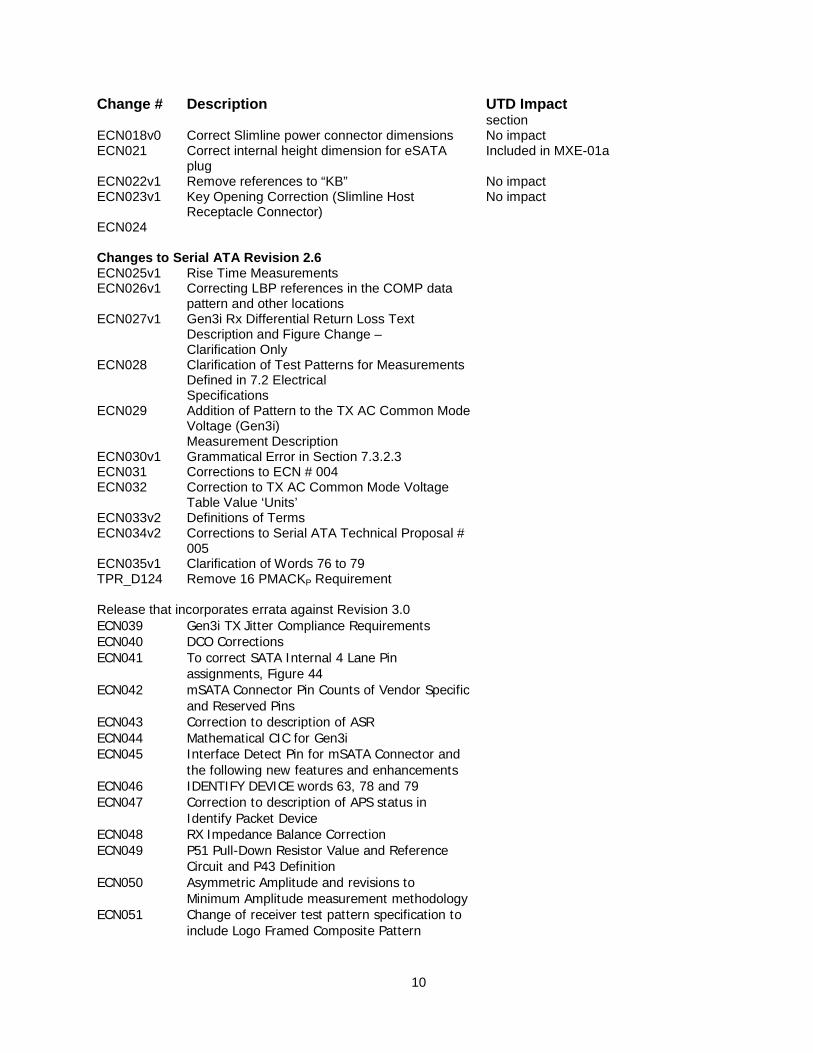
Change # Description UTD Impact section
ECN018v0 Correct Slimline power connector dimensions No impact ECN021 Correct internal height dimension for eSATA
plug Included in MXE-01a
ECN022v1 Remove references to “KB” No impact ECN023v1 Key Opening Correction (Slimline Host
Receptacle Connector) No impact
ECN024 Changes to Serial ATA Revision 2.6 ECN025v1 Rise Time Measurements ECN026v1 Correcting LBP references in the COMP data
pattern and other locations
ECN027v1 Gen3i Rx Differential Return Loss Text Description and Figure Change – Clarification Only
ECN028 Clarification of Test Patterns for Measurements Defined in 7.2 Electrical Specifications
ECN029 Addition of Pattern to the TX AC Common Mode Voltage (Gen3i) Measurement Description
ECN030v1 Grammatical Error in Section 7.3.2.3 ECN031 Corrections to ECN # 004 ECN032 Correction to TX AC Common Mode Voltage
Table Value ‘Units’
ECN033v2 Definitions of Terms ECN034v2 Corrections to Serial ATA Technical Proposal #
005
ECN035v1 Clarification of Words 76 to 79 TPR_D124 Remove 16 PMACKP Requirement Release that incorporates errata against Revision 3.0 ECN039 Gen3i TX Jitter Compliance Requirements ECN040 DCO Corrections ECN041 To correct SATA Internal 4 Lane Pin
assignments, Figure 44
ECN042 mSATA Connector Pin Counts of Vendor Specific and Reserved Pins
ECN043 Correction to description of ASR ECN044 Mathematical CIC for Gen3i ECN045 Interface Detect Pin for mSATA Connector and
the following new features and enhancements
ECN046 IDENTIFY DEVICE words 63, 78 and 79 ECN047 Correction to description of APS status in
Identify Packet Device
ECN048 RX Impedance Balance Correction ECN049 P51 Pull-Down Resistor Value and Reference
Circuit and P43 Definition
ECN050 Asymmetric Amplitude and revisions to Minimum Amplitude measurement methodology
ECN051 Change of receiver test pattern specification to include Logo Framed Composite Pattern
11
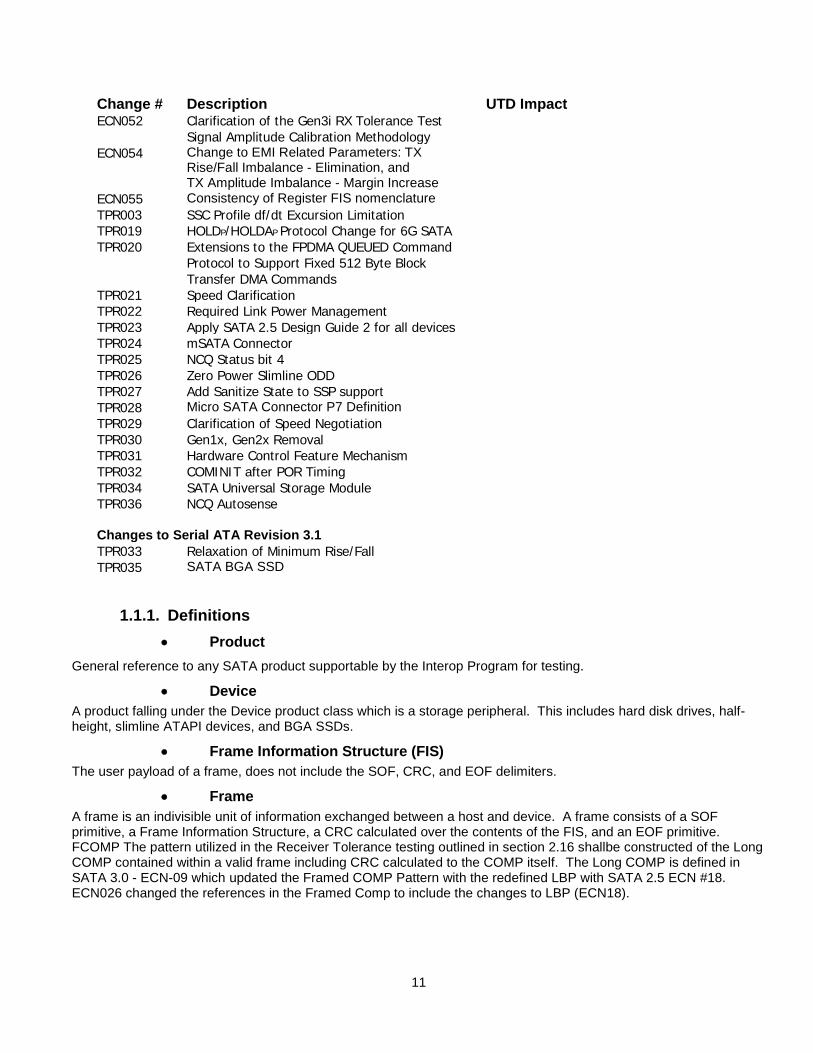
Change # Description UTD Impact ECN052 Clarification of the Gen3i RX Tolerance Test
Signal Amplitude Calibration Methodology
ECN054 Change to EMI Related Parameters: TX Rise/Fall Imbalance - Elimination, and TX Amplitude Imbalance - Margin Increase
ECN055 Consistency of Register FIS nomenclature TPR003 SSC Profile df/dt Excursion Limitation TPR019 HOLDP/HOLDAP Protocol Change for 6G SATA TPR020 Extensions to the FPDMA QUEUED Command
Protocol to Support Fixed 512 Byte Block Transfer DMA Commands
TPR021 Speed Clarification TPR022 Required Link Power Management TPR023 Apply SATA 2.5 Design Guide 2 for all devices TPR024 mSATA Connector TPR025 NCQ Status bit 4 TPR026 Zero Power Slimline ODD TPR027 Add Sanitize State to SSP support TPR028 Micro SATA Connector P7 Definition TPR029 Clarification of Speed Negotiation TPR030 Gen1x, Gen2x Removal TPR031 Hardware Control Feature Mechanism TPR032 COMINIT after POR Timing TPR034 SATA Universal Storage Module TPR036 NCQ Autosense
Changes to Serial ATA Revision 3.1 TPR033 Relaxation of Minimum Rise/Fall TPR035 SATA BGA SSD
1.1.1. Definitions • Product
General reference to any SATA product supportable by the Interop Program for testing.
• Device A product falling under the Device product class which is a storage peripheral. This includes hard disk drives, half-height, slimline ATAPI devices, and BGA SSDs.
• Frame Information Structure (FIS) The user payload of a frame, does not include the SOF, CRC, and EOF delimiters.
• Frame A frame is an indivisible unit of information exchanged between a host and device. A frame consists of a SOF primitive, a Frame Information Structure, a CRC calculated over the contents of the FIS, and an EOF primitive. FCOMP The pattern utilized in the Receiver Tolerance testing outlined in section 2.16 shallbe constructed of the Long COMP contained within a valid frame including CRC calculated to the COMP itself. The Long COMP is defined in SATA 3.0 - ECN-09 which updated the Framed COMP Pattern with the redefined LBP with SATA 2.5 ECN #18. ECN026 changed the references in the Framed Comp to include the changes to LBP (ECN18).
12
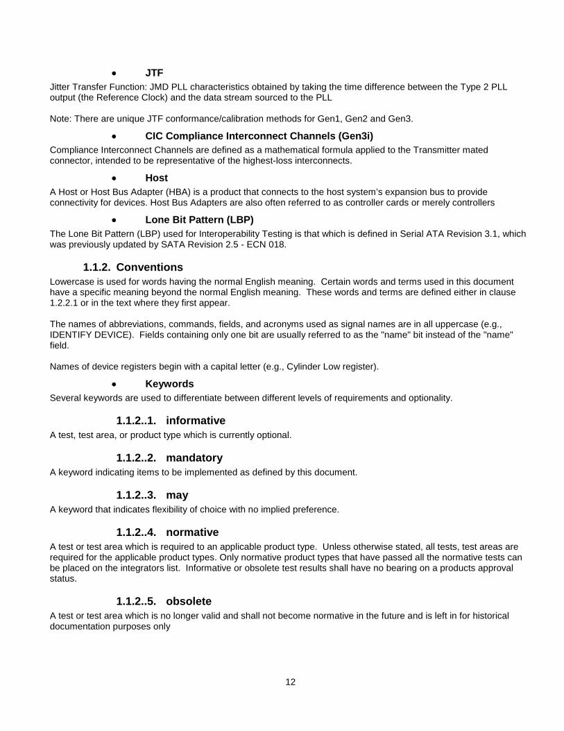
• JTF Jitter Transfer Function: JMD PLL characteristics obtained by taking the time difference between the Type 2 PLL output (the Reference Clock) and the data stream sourced to the PLL Note: There are unique JTF conformance/calibration methods for Gen1, Gen2 and Gen3.
• CIC Compliance Interconnect Channels (Gen3i) Compliance Interconnect Channels are defined as a mathematical formula applied to the Transmitter mated connector, intended to be representative of the highest-loss interconnects.
• Host A Host or Host Bus Adapter (HBA) is a product that connects to the host system’s expansion bus to provide connectivity for devices. Host Bus Adapters are also often referred to as controller cards or merely controllers
• Lone Bit Pattern (LBP) The Lone Bit Pattern (LBP) used for Interoperability Testing is that which is defined in Serial ATA Revision 3.1, which was previously updated by SATA Revision 2.5 - ECN 018.
1.1.2. Conventions Lowercase is used for words having the normal English meaning. Certain words and terms used in this document have a specific meaning beyond the normal English meaning. These words and terms are defined either in clause 1.2.2.1 or in the text where they first appear. The names of abbreviations, commands, fields, and acronyms used as signal names are in all uppercase (e.g., IDENTIFY DEVICE). Fields containing only one bit are usually referred to as the "name" bit instead of the "name" field. Names of device registers begin with a capital letter (e.g., Cylinder Low register).
• Keywords Several keywords are used to differentiate between different levels of requirements and optionality.
1.1.2..1. informative A test, test area, or product type which is currently optional.
1.1.2..2. mandatory A keyword indicating items to be implemented as defined by this document.
1.1.2..3. may A keyword that indicates flexibility of choice with no implied preference.
1.1.2..4. normative A test or test area which is required to an applicable product type. Unless otherwise stated, all tests, test areas are required for the applicable product types. Only normative product types that have passed all the normative tests can be placed on the integrators list. Informative or obsolete test results shall have no bearing on a products approval status.
1.1.2..5. obsolete A test or test area which is no longer valid and shall not become normative in the future and is left in for historical documentation purposes only
13
1.1.2..6. optional A keyword that describes test requirements that are not required by this document. However, if any optional compliance point defined by the document is implemented, the feature shall be implemented in the way defined by the Serial ATA standard.
1.1.2..7. shall A keyword indicating a mandatory requirement. Designers are required to implement all such mandatory requirements to ensure interoperability with other Serial ATA standard conformant products.
1.1.2..8. should A keyword indicating flexibility of choice with a strongly preferred alternative. Equivalent to the phrase “it is recommended”.
1.2. Product Classes Due to the difference in architecture and design of Serial ATA products, the test requirements shallbe distinguishable between the following types of products:
• Device : hard disk drive, half-height ATAPI device, slimline ATAPI device, eSATA device, or SSD BGA • Cable (Standard internal or eSATA) • Host : HBA, chipset, add-in controller, or eSATA • Port Multiplier (internal or eSATA)
Each test associated with a Specification requirement may have separately defined Expected Behavior for each of the above product classes. In each case, there may be different methodology for both testing the test requirement and determining the pass/fail criteria. Each test requirement shallinclude the following: Expected Behavior, Measurement Requirements, and Pass/Fail Criteria. The general definition of these subjects is below.
1.2.1. Expected Behavior All of the test requirements have expected behavior as defined in Serial ATA Revision 3.1. All of the expected behavior for each test requirement directly shall refer to the appropriate Serial ATA Specification requirement(s) being tested.
1.2.2. Measurement Requirements Each test requirement contains detailed information necessary for developing tests for verification of the referenced Serial ATA requirement. This information could include types of equipment, testing methodologies, test setup routines, and other helpful information.
1.2.3. Pass/Fail Criteria The Pass/Fail criteria defined shallbe clear and concise, and include specific information necessary to determine passing or failing of a test. Actual results gathered during testing shall be documented in addition to determination of pass vs. fail for a test.
1.3. Methods of Implementation A Method of Implementation (MOI) is defined as documentation specifying test tool details and procedures for the specific use of verifying the different Interoperability test areas. In the future a template for development of a MOI for a specific test tool may be developed, but at this time a MOI, at a minimum, shall include the following:
• Hardware equipment model number(s) • Software revision number(s) • Hardware dependencies (e.g. test fixtures) • Product dependencies (e.g. BIST modes, patterns) • Detailed procedures for using the equipment to verify the specific Interop test requirements • Procedures for extraction of results
14
• Approximate execution time of specific Interop test requirements There are different MOI classes which are specific to the different test areas included in this Unified Test Document. Any test tool approved for use in Interoperability Testing shall fall under test execution within one of the following MOI classes:
• Digital/protocol (device/host or port multiplier only) • Phy electrical (device/host only) • Phy TX/RX requirements (device/host only) • RSG requirements (device/host or eSATA only) • Receiver Jitter Tolerance (device/host only) • Mechanical (device/host or eSATA only) • Cable mechanical (internal or eSATA cable only) • Cable electrical (internal or eSATA cable only) • System interoperability (device/host only)
It is feasible that separate MOIs are developed for each type of equipment used depending on the class of testing, or that a single MOI is used to cover an entire test class including the details for several pieces of test tool equipment. This shall be determined by the appropriate test tool vendors with considerations from the SATA-IO.
1.4. Test Product Considerations
1.4.1. Common Host/Device/Port Multiplier BIST Considerations For many of the Phy electrical tests, it is required that a product (Host/Device/Port Multiplier and eSATA versions of these) is able to transmit and/or loop back patterns which are identified within the Serial ATA Revision 3.1 or this document. There are standard ways of doing this through the BIST protocol per definition within the Specification. If a product does not specifically support either BIST T, A, S, and/or BIST L capabilities then the vendor needs to bring all equipment to support vendor unique methods for completely emulating BIST T, A, S and BIST L. Note that this vendor unique process can have no substantial impact to the test during interoperability testing (e.g. significant growth in test execution time or complexity of equipment calibration/setup).
1.4.2. Device specific considerations A device vendor is required to supply at least three samples. In some cases up to two samples maybe run through testing in parallel at a given time. The third sample should be available for backup in case of unexpected errors or failures.
1.4.3. Cable Considerations If a cable assembly product family consists of cables which differ only in their length (the connector design, cable construction, and assembly method is identical) and if the shortest and longest lengths pass the test requirements then all intermediate lengths are considered to be passing. A cable vendor is required to supply at least two identical samples of each length tested.
1.4.4. Host Considerations A host vendor is required to supply at least two samples. In some cases up to two samples may be run through testing in parallel at a given time. In most cases, the second or third sample shall not be secured within a chassis or platform case, as this sample may be used specifically for mechanical testing. Prior to execution of any testing on a host, a “worst port” for each port type (i.e. internal SATA and/or eSATA) shall be identified. The intent of identifying a worst port is not to validate each port to the Specification, but to simply identify the worst port based on a single relative measurement across all ports within a host. The Interoperability Tests shall then, at a minimum, be executed on the worst port identified per the procedure below.
• Power-on host and ensure test ports are enabled & functional. Run the following on each individual port. o Connect device and complete OOB sequence
15
o Execute and record results for the typical Total Jitter (TJ) measurement using LBP while the host is in NRZ idle following OOB
• The “worse port” is identified as that which has the highest TJ value recorded on the measurement above Relative to the Interface Power Management tests (see Section 2.5), it is expected that the host product manufacturer supply a facility (software, or hardware automation) which shall initiate power management state requests in order to support host-initiated test execution – this is only required if the host product claims support for the host-initiated power management capability.
1.4.5. Port Multiplier Considerations A port multiplier vendor is required to supply at least two samples. In some cases up to two samples may be run through testing at a given time. In most cases, the second or third sample shall not be secured within a chassis or platform case, as this sample may be used specifically for mechanical testing. Prior to execution of any testing on a port multiplier, a “worst port” shall be identified. The intent of identifying a worst port is not to validate each port to the Specification, but to simply identify the worst port based on a single relative measurement across all ports within a port multiplier. The Interoperability Tests shall, at a minimum, then be executed on the worst port identified per the procedure below.
• Power-on port multiplier and ensure test ports are enabled & functional. Run the following on each individual port.
o If it is a device port, connect a device and complete OOB sequence o If it is a host port, connect a host and complete OOB sequence o Execute and record results for the typical Total Jitter (TJ) measurement using LBP while the port
multiplier port is in NRZ idle following OOB • The “worse port” is identified as that which has the highest TJ value recorded on the measurement above
Relative to the Interface Power Management tests (see section 3)), it is expected that the port multiplier product manufacturer supply a facility (software, or hardware automation) which shall initiate power management state requests in order to support port multiplier -initiated test execution – this is only required if the host product claims support for the port multiplier -initiated power management capability.
2. Interoperability Specification Test Summary Table 1 outlines the test requirements for the different types of Serial ATA units under test.
Table 1 - Test Requirements by Product Class Test GRP
Sec # Test Req.
Area Device/MicroS
ATA HDD
Device ATAPI
Internal Cable Signal
Internal Cable Power
Host Port Multi-plier *
eSATA Cable*
eSATA host/
device*
GTR 2.1 GTR-01 Digital M M -- -- -- M -- I GTR-02 Digital F F -- -- -- F -- I GTR-03 Digital M M -- -- -- M -- I GTR-04 Digital M M -- -- -- M -- I GTR-05 Digital * * -- -- -- * -- I NCQ 2.2 NCQ-01 Digital F -- -- -- -- F -- I NCQ-02 Digital F -- -- -- -- F -- I NCQ-03 Digital F -- -- -- -- F -- I NCQ-04 Digital F -- -- -- -- F -- I NCQ-05 Digital F -- -- -- -- F -- I ASR 2.3 ASR-01 Digital M M -- -- -- M -- I ASR-02 Digital F F -- -- -- F -- I ASR-03 Digital -- -- -- -- F -- -- F/-- SSP 2.4 SSP-01 Digital F -- -- -- -- F -- I SSP-02 Digital F -- -- -- -- F -- I SSP-03 Digital F F -- -- -- F -- I
16
Test GRP
Sec # Test Req.
Area Device/MicroS
ATA HDD
Device ATAPI
Internal Cable Signal
Internal Cable Power
Host Port Multi-plier *
eSATA Cable*
eSATA host/
device*
SSP-04 Digital F -- -- -- -- F -- I SSP-05 Digital F F -- -- -- F -- I SSP-06 Digital F F -- -- -- F -- I SSP-07 Digital F -- -- -- -- F -- I SSP-08 Digital F F -- -- -- F -- I SSP-09 Digital F F -- -- -- F -- I SSP-10 Digital F F -- -- -- F -- I SSP-11 Digital F -- -- -- -- F -- I SSP-12 Digital F -- -- -- -- F -- I IPM 2.5 IPM-01 Digital F F -- -- F -- -- I IPM-02 Digital F F -- -- F -- -- I IPM-03 Digital F F -- -- F -- -- I IPM-04 Digital F F -- -- F -- -- I IPM-05 Digital F F -- -- F -- -- I IPM-06 Digital F F -- -- F -- -- I IPM-07 Digital F F -- -- -- -- -- I IPM-08 Digital F F -- -- -- -- -- I IPM-09 Digital F F -- -- F -- -- I IPM-10 Digital F F -- -- F -- -- I IPM-11 Digital F F -- -- F -- -- I DOF 2.6 DOF-01 Digital -- F -- -- -- -- -- I DOF-02 Digital F F -- -- -- -- -- I MCI 2.7 MCI-01 Cable -- -- M -- -- -- -- -- MCI-02 Cable -- -- M -- -- -- -- -- MCI-03 Cable -- -- F -- -- -- -- -- MCI-04 Cable -- -- F -- -- -- -- -- MCX MCX-05 Cable -- -- M -- -- -- I -- MCE MCE-01 Cable -- -- -- -- -- -- M -- SI 2.7.6 SI-01 Cable -- -- M -- -- -- I -- SI-02 Cable -- -- M -- -- -- I -- SI-03 Cable -- -- M -- -- -- I -- SI-04 Cable -- -- M -- -- -- I -- SI-05 Cable -- -- M -- -- -- I-n -- SI-06 Cable -- -- M -- -- -- I-n -- SI-07 Cable -- -- M -- -- -- I-n -- SI-08 Cable -- -- M -- -- -- I -- SI-09 Cable -- -- M -- -- -- I -- MDI 2.9 MDI-01 Mech M M -- -- -- -- -- -- MDI-02 Mech M M -- -- -- -- -- -- MDP 2.10 MDP-01 Mech M M -- -- -- -- -- -- MHI 2.11 MHI-01 Mech -- -- -- -- * -- -- --/* MXE*
2.12 MXE-01 Mech -- -- -- -- -- -- -- M/M
PHY 2.13 PHY-01 Phy M M -- -- M F -- I PHY-02 Phy M M -- -- M F -- I PHY-03 Phy F F -- -- F F -- I PHY-04 Phy F F -- -- F F -- I TX 2.14 TX-01 RX/TX M M -- -- M M -- I TX-02 RX/TX * * -- -- * * -- I TX-03 RX/TX F F -- -- F F-n -- I-n TX-04 RX/TX F F -- -- F F -- I TX-05 RX/TX F F -- -- F F-n -- I-n TX-06 RX/TX M M -- -- M M -- I TX-07 RX/TX M M -- -- M M -- I TX-08 RX/TX M M -- -- M M -- I
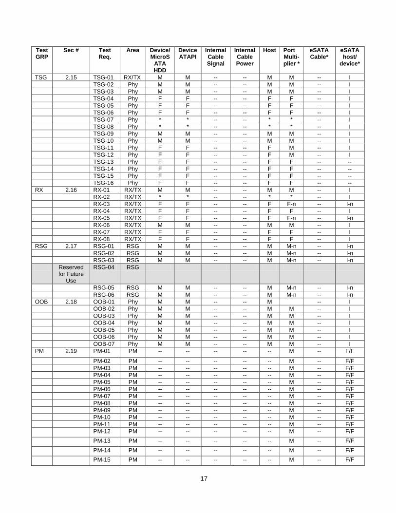
17
Test GRP
Sec # Test Req.
Area Device/MicroS
ATA HDD
Device ATAPI
Internal Cable Signal
Internal Cable Power
Host Port Multi-plier *
eSATA Cable*
eSATA host/
device*
TSG 2.15 TSG-01 RX/TX M M -- -- M M -- I TSG-02 Phy M M -- -- M M -- I TSG-03 Phy M M -- -- M M -- I TSG-04 Phy F F -- -- F F -- I TSG-05 Phy F F -- -- F F -- I TSG-06 Phy F F -- -- F F -- I TSG-07 Phy * * -- -- * * -- I TSG-08 Phy * * -- -- * * -- I TSG-09 Phy M M -- -- M M -- I TSG-10 Phy M M -- -- M M -- I TSG-11 Phy F F -- -- F M -- I TSG-12 Phy F F -- -- F M -- I TSG-13 Phy F F -- -- F F -- -- TSG-14 Phy F F -- -- F F -- -- TSG-15 Phy F F -- -- F F -- -- TSG-16 Phy F F -- -- F F -- -- RX 2.16 RX-01 RX/TX M M -- -- M M -- I RX-02 RX/TX * * -- -- * * -- I RX-03 RX/TX F F -- -- F F-n -- I-n RX-04 RX/TX F F -- -- F F -- I RX-05 RX/TX F F -- -- F F-n -- I-n RX-06 RX/TX M M -- -- M M -- I RX-07 RX/TX F F -- -- F F -- I RX-08 RX/TX F F -- -- F F -- I RSG 2.17 RSG-01 RSG M M -- -- M M-n -- I-n RSG-02 RSG M M -- -- M M-n -- I-n RSG-03 RSG M M -- -- M M-n -- I-n Reserved
for Future Use
RSG-04 RSG
RSG-05 RSG M M -- -- M M-n -- I-n RSG-06 RSG M M -- -- M M-n -- I-n OOB 2.18 OOB-01 Phy M M -- -- M -- I OOB-02 Phy M M -- -- M M -- I OOB-03 Phy M M -- -- M M -- I OOB-04 Phy M M -- -- M M -- I OOB-05 Phy M M -- -- M M -- I OOB-06 Phy M M -- -- M M -- I OOB-07 Phy M M -- -- M M -- I PM 2.19 PM-01 PM -- -- -- -- -- M -- F/F
PM-02 PM -- -- -- -- -- M -- F/F PM-03 PM -- -- -- -- -- M -- F/F PM-04 PM -- -- -- -- -- M -- F/F PM-05 PM -- -- -- -- -- M -- F/F PM-06 PM -- -- -- -- -- M -- F/F PM-07 PM -- -- -- -- -- M -- F/F PM-08 PM -- -- -- -- -- M -- F/F PM-09 PM -- -- -- -- -- M -- F/F PM-10 PM -- -- -- -- -- M -- F/F PM-11 PM -- -- -- -- -- M -- F/F PM-12 PM -- -- -- -- -- M -- F/F PM-13 PM -- -- -- -- -- M -- F/F PM-14 PM -- -- -- -- -- M -- F/F PM-15 PM -- -- -- -- -- M -- F/F
18
Test GRP
Sec # Test Req.
Area Device/MicroS
ATA HDD
Device ATAPI
Internal Cable Signal
Internal Cable Power
Host Port Multi-plier *
eSATA Cable*
eSATA host/
device*
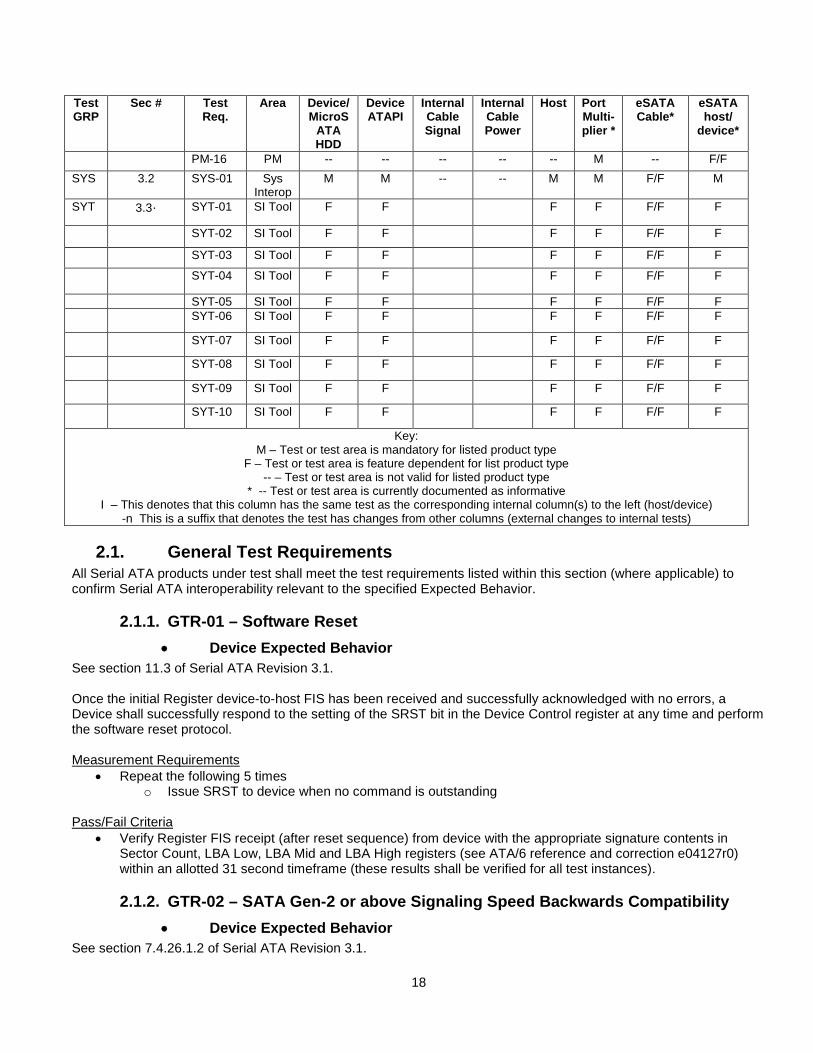
PM-16 PM -- -- -- -- -- M -- F/F SYS 3.2 SYS-01 Sys
Interop M M -- -- M M F/F M
SYT 3.3· SYT-01 SI Tool F F F F F/F F
SYT-02 SI Tool F F F F F/F F
SYT-03 SI Tool F F F F F/F F
SYT-04 SI Tool F F F F F/F F
SYT-05 SI Tool F F F F F/F F SYT-06 SI Tool F F F F F/F F
SYT-07 SI Tool F F F F F/F F
SYT-08 SI Tool F F F F F/F F
SYT-09 SI Tool F F F F F/F F
SYT-10 SI Tool F F F F F/F F
Key: M – Test or test area is mandatory for listed product type
F – Test or test area is feature dependent for list product type -- – Test or test area is not valid for listed product type
* -- Test or test area is currently documented as informative I – This denotes that this column has the same test as the corresponding internal column(s) to the left (host/device)
-n This is a suffix that denotes the test has changes from other columns (external changes to internal tests)
2.1. General Test Requirements All Serial ATA products under test shall meet the test requirements listed within this section (where applicable) to confirm Serial ATA interoperability relevant to the specified Expected Behavior.
2.1.1. GTR-01 – Software Reset • Device Expected Behavior
See section 11.3 of Serial ATA Revision 3.1. Once the initial Register device-to-host FIS has been received and successfully acknowledged with no errors, a Device shall successfully respond to the setting of the SRST bit in the Device Control register at any time and perform the software reset protocol. Measurement Requirements
• Repeat the following 5 times o Issue SRST to device when no command is outstanding
Pass/Fail Criteria
• Verify Register FIS receipt (after reset sequence) from device with the appropriate signature contents in Sector Count, LBA Low, LBA Mid and LBA High registers (see ATA/6 reference and correction e04127r0) within an allotted 31 second timeframe (these results shall be verified for all test instances).
2.1.2. GTR-02 – SATA Gen-2 or above Signaling Speed Backwards Compatibility • Device Expected Behavior
See section 7.4.26.1.2 of Serial ATA Revision 3.1.
19
If a device claims support for Serial ATA Gen-2 or above (n>=2) signaling speed (Word 76 bit 2 or above (n>=2) set to one in IDENTIFY DEVICE or IDENTIFY PACKET DEVICE data), then it shall also support Serial ATA signaling speed below it (<n) (Word 76 bit below n, i.e. (n-1) to 1 (n>=2) set to one in IDENTIFY DEVICE or IDENTIFY PACKET DEVICE data). In addition to verifying the IDENTIFY DEVICE or IDENTIFY PACKET DEVICE contents, support shall be verified by ensuring compatibility and interoperability with Gen-1 and above up to Gen-n (n>=2) host. Details on how this testing is done is not specified in this document. Measurement Requirements
• Check Word 76 bit 2 or above in IDENTIFY DEVICE or IDENTIFY PACKET DEVICE data (set to one) • If the above are true, then run the following test when connected to a Gen-1 and above up to Gen-n (n>=2)
host - Check Word 76 bit (n-1) to 1 (n>=2) in IDENTIFY DEVICE or IDENTIFY PACKET DEVICE data
(set to one) - Complete OOB sequence at least 10 times
Pass/Fail Criteria
• Values below shall be confirmed when tested in connection with Gen-1 and above up to Gen-n (n>=2) host - Verify IDENTIFY DEVICE or IDENTIFY PACKET DEVICE contents including:
If Word 76 bit 2 or above (n>=2) set to one, then Word 76 bit below n, i.e. (n-1) to 1 set to one - Verify Register FIS receipt (after each OOB sequence) from device with the appropriate signature
contents in Sector Count, LBA Low, LBA Mid and LBA High registers. (see ATA/6 reference and correction e04127r0)
2.1.3. GTR-03 – DMA Protocol Support • Device Expected Behavior
See sections 13.2.1 and 13.2.2 of Serial ATA Revision 3.1. DMA support can be verified through Word 49 bit 8 in IDENTIFY DEVICE or IDENTIFY PACKET DEVICE data. This bit shall be set to one for all Serial ATA devices. The type of DMA supported can be verified through the IDENTIFY DEVICE or IDENTIFY PACKET DEVICE command data: Word 63, bits 2:0 for Multiword DMA (MWDMA) and Word 88 bits 6:0 for Ultra DMA (UDMA). If both types of DMA are supported, the UDMA type shall be selected. If only one type of DMA is supported, then the supported type shall be selected. The highest supported transfer rate of the selected DMA type shall be selected. Measurement Requirements
• Check Word 49 bit 8 in IDENTIFY DEVICE or IDENTIFY PACKET DEVICE data (set to one) • If the above are true, then run the appropriate tests below
For consistency, it is required that the FCOMP pattern as defined in the Specification is used as the data set for the tests below. Note that in some cases dependent on transfer size that it may not be feasible to include complete iterations of the FCOMP pattern within the data set being used. There are several test scenarios that are required when testing a HDD for this test requirement, all of which shall be tested 5 times each to verify passing of the test:
• Issue IDENTIFY DEVICE to device • Issue and complete WRITE DMA command to device with transfer size of less than or equal to 8Kbytes,
followed by issue and completion of READ DMA command to device to the same disk location that the previous write was completed. The test shall verify that the contents read have the same values that were previously written.
20
• Issue and complete WRITE DMA command to device with transfer size of greater than 8Kbytes but less than or equal to 128Kbytes, followed by issue and completion of READ DMA command to device to the same disk location that the previous write was completed. The test shall verify that the contents read have the same values that were written initially.
There are several test scenarios that are required when testing an ATAPI read-only device for this test requirement, all of which shall be tested 5 times each to verify passing of the test. The tests below are for ATAPI devices which only support reading from media (e.g. CDROM, DVDROM, etc…).
• Issue IDENTIFY PACKET DEVICE to device • Issue and complete one tracks worth of read commands using the DMA protocol with transfer size of less
than or equal to 8Kbytes, followed by issue and completion of another tracks worth of read commands using the DMA protocol to the same disk location that the previous reads were completed. The test shall verify that the contents read have the same values that were read initially.
• Issue and complete one tracks worth of read commands using the DMA protocol with transfer size of greater than 8Kbytes but less than or equal to 128Kbytes, followed by issue and completion of another tracks worth of read commands using the DMA protocol to the same disk location that the previous reads were completed. The test shall verify that the contents read have the same values that were read initially.
There are several test scenarios that are required when testing an ATAPI device for this test requirement, all of which shall be tested 5 times each to verify passing of the test. The tests below are for ATAPI devices which support writing to media.
• Issue IDENTIFY PACKET DEVICE to device • Issue and complete one tracks worth of write commands using the DMA protocol with transfer size of less
than or equal to 8Kbytes, followed by issue and completion of one tracks worth of read commands using the DMA protocol to the same disk locations where the previous writes were completed. The test shall verify that the contents read have the same values that were previously written.
• Issue and complete one tracks worth of write commands using the DMA protocol with transfer size of greater than 8Kbytes but less than or equal to 128Kbytes, followed by issue and completion of one tracks worth of read commands using the DMA protocol to the same disk locations where the previous writes were completed. The test shall verify that the contents read have the same values that were previously written.
Pass/Fail Criteria
• Verify Word 49 bit 8 set to one in IDENTIFY DEVICE or IDENTIFY PACKET DEVICE • Verify that data read is equal to data initially written (or read in case of ATAPI read-only device) • If neither MWDMA nor UDMA type is supported, then the result is fail
2.1.4. GTR-04 – General SATA Support • Device Expected Behavior
See sections 13.2.1 and 13.2.2 of Serial ATA Revision 3.1. For all Serial ATA devices, the entire contents of Word 93 in IDENTIFY DEVICE or IDENTIFY PACKET DEVICE data shall be cleared to zero. For all Serial ATA devices, support for the 1.5 Gbps interface rate is required. This can be verified through Word 76 bit 1 in IDENTIFY DEVICE or IDENTIFY PACKET DEVICE data. This bit shall be set to one for all Serial ATA devices. If Word76 is not 0000h or FFFFh, the device claims compliance with the Serial ATA Specification and supports the signaling rate indicated in bits 1-3. Since Serial ATA supports generational compatibility, multiple bits may be set. Bit 0 is reserved and shall be cleared to zero (thus a Serial ATA device has at least one bit cleared in this field and at least one bit set providing clear differentiation). Word 77-79 bit 0 shall be cleared to zero.
21
Measurement Requirements • Issue IDENTIFY DEVICE or IDENTIFY PACKET DEVICE to device
Pass/Fail Criteria
• Verify Word 93 is cleared to zero in IDENTIFY DEVICE or IDENTIFY PACKET DEVICE • Verify Word 76 bit 1 is set to one in IDENTIFY DEVICE or IDENTIFY PACKET DEVICE • Verify Word 76-79 bit 0 is cleared to zero
2.1.5. GTR-05 : Unrecognized FIS receipt (Informative) • Device Expected Behavior
See section 10.3.1.1 of Serial ATA Revision 3.1. The receiver of an “unrecognized FIS” shall follow the link layer state machine definitions in section 9.7 of the Serial ATA Revision 3.1 upon receipt of an “unrecognized FIS”. The expected response is status return with an R_ERR. Note that determination of any FIS being ‘unrecognized’ is done by the recipient of the FIS. The contents of the “Unrecognized FIS” are not defined by this document, but shall be described in each applicable MOI. Measurement Requirements
• Transmit undefined FIS to device Pass/Fail Criteria
• Verify R_ERR response from device
2.2. Native Command Queuing The Native Command Queuing (NCQ) test requirements are determined by the requirements of the feature as defined in Serial ATA Revision 3.1. All of the test requirements listed in this section require that support for NCQ is claimed by the product for verification of the Expected Behavior. Support for NCQ can be verified by reading Word 76 bit 8 set to one in IDENTIFY DEVICE data.
2.2.1. NCQ-01 : Forced Unit Access • Device Expected Behavior
See sections 11.14 and 13.6.4 of Serial ATA Revision 3.1. Devices that support the NCQ commands (READ FPDMA QUEUED and WRITE FPDMA QUEUED) shall support the Force Unit Access (FUA) bit. For WRITE FPDMA QUEUED when the FUA bit is set to one, the data shall be written to the storage media before completing the command. Due to the limitations in testability of specific device functions, this test shall be limited to verifying the compatibility of a device in receiving a command with the FUA bit set to one. This test shall not completely verify whether data was written to non-volatile media. Measurement Requirements
• Check Word 76 bit 8 in IDENTIFY DEVICE (set to one) • If the above is true, then run the following test
o Issue and complete WRITE FPDMA QUEUED with FUA bit set. o Issue and complete READ FPDMA QUEUED to the same disk location.
Pass/Fail Criteria
• Verify that data read is equal to data written.
22
2.2.2. NCQ-02 : Read Log Ext log page 10h support • Device Expected Behavior
See section 13.6.3.2.1 of Serial ATA Revision 3.1. If a device claims support for Native Command Queuing (Word 76 bit 8 set to one in IDENTIFY DEVICE data), then it shall also support READ LOG EXT log page 10h and the General Purpose Logging feature set. Support for READ LOG EXT log page 10h is reflected in the General Purpose Log Directory page (log page 0) by having the value 1 at offset 20h and the value 0 at offset 21h of that log page to indicate existence of a log page at address 10h of 1-page in length. A READ LOG EXT log page 10h command shall be issued and completed without error. No contents shall be validated. Measurement Requirements
• Check Word 76 bit 8 in IDENTIFY DEVICE (set to one) • Check Word 87 bit 5 in IDENTIFY DEVICE (set to one) • If the above is true, then run the following test
o Issue READ LOG EXT to log page 00h o Issue READ LOG EXT to log page 10h
Pass/Fail Criteria
• Verify successful completion & data transfer for log page 0h • Verify offset 20h of log page 00h contains value of 1 • Verify offset 21h of log page 00h contains value of 0 • Verify successful completion & data transfer for log page 10h, it is NOT necessary that the contents of the log
page are verified for specific values
2.2.3. NCQ-03 : Intermix of Legacy and NCQ commands • Device Expected Behavior
See section 13.6.2 of Serial ATA Revision 3.1. Upon receiving a legacy ATA command while a native queued command is outstanding, an error has occurred and the device shall perform necessary state cleanup to return to a state with no commands pending. Legacy ATA commands include all commands other than the READ FPDMA QUEUED and WRITE FPDMA QUEUED commands. The device shall signal the error condition to the host by transmitting a Register FIS to the host with the ERR bit set to one and the BSY bit cleared to zero in the Status field, and the ABRT bit set to one in the Error field. Upon detecting an error when there are one or more NCQ commands outstanding, the device shall stop processing commands until a READ LOG EXT command with a specified log page of 10h or reset is issued. Upon receipt of the READ LOG EXT command, the device shall send a Set Device Bits FIS to discard all commands in the pending device queue, followed by data for the log page. The READ LOG EXT page shall reflect that the error condition was a result of a legacy ATA command having been issued by having the NQ bit set to one. The device shall not continue command processing for any of the outstanding commands following this error. If no prior NCQ error has occurred and a device has received a READ LOG EXT command while there are NCQ commands outstanding, the device shall respond as described above as having received a legacy ATA command while one or more native queued commands are outstanding. Measurement Requirements
• Check Word 76 bit 8 in IDENTIFY DEVICE (set to one) • If the above is true, then run the following test
• Check Word 75 bits 4:0 to verify maximum queue depth reported by device
23
• Issue at least X random FPDMA QUEUED commands (read or write), where X is the maximum queue depth reported above
• Issue a legacy ATA command using one of the following (NOTE that the test shall be run a total of four times to ensure each legacy ATA command listed below is used for the test):
o IDENTIFY DEVICE o PIO write o DMA read o Read Log Ext with log page 10h
• Verify Register FIS receipt with ERR bit set to 1, DRDY bit set to 1, DF bit cleared to 0, BSY bit cleared to zero and DRQ bit cleared to 0
o Issue Read Log Ext to log page 10h Pass/Fail Criteria
• Verify receipt of Register FIS with error • Verify SDB receipt with ERR bit cleared to zero, DRDY set to 1, DF bit cleared to zero, BSY bit cleared to
zero, DRQ bit cleared to zero, the ‘I’ bit cleared to zero, and the SActive field set to FFFFFFFFh. • Verify that the NQ bit is set to one in the data within log page 10h • Verify that the checksum is correct in the data within Log page 10h • NOTE – there is opportunity for a device to complete all outstanding commands prior to the host being
able to send the legacy ATA command. In these cases, the device may not be failed for this particular test.
2.2.4. NCQ-04 : Device response to malformed NCQ command • Device Expected Behavior
See section 13.6.2.and 13.6.4.1 of Serial ATA Revision 3.1. Malformed commands could include the following situations:
• Specified LBA is out of the device supported range
• Duplicate tag value for outstanding NCQ command
• TAG value is out of the device supported range, only in the case that the device reports support for less than 32 outstanding commands
In response to a malformed READ FPDMA QUEUED or WRITE FPDMA QUEUED command due to a duplicate tag or out of range tag, the device shall transmit a Register FIS to the host with the ERR bit set to one, and the BSY bit cleared to zero in the Status register. The ‘I’ bit shall be set to one. The ABRT bit shall be set in the Error field. The device shall stop processing commands until a READ LOG EXT command with a specified log page of 10h or reset is issued. Upon receipt of the READ LOG EXT command, the device shall send a Set Device Bits FIS to discard all commands in the pending device queue, followed by data for the log page. The READ LOG EXT page shall have the NQ bit cleared to zero. The TAG field within the log page shall contain the tag associated with the NCQ command which failed. In response to a malformed READ FPDMA QUEUED or WRITE FPDMA QUEUED command due to an LBA out of range, the device may report the error in one of two ways:
• Transmit a Register FIS to the host with the ERR bit set to one, and the BSY bit cleared to zero in the Status register. The ‘I’ bit shall be set to one. Either the ABRT bit or IDNF bit shall be set to one in the Error field. The device shall stop processing commands until a READ LOG EXT command with a specified log page of 10h or reset is issued. Upon receipt of the READ LOG EXT command, the device shall send a Set Device Bits FIS to discard all commands in the pending device queue, followed by data for the log page. The READ LOG EXT page shall have the NQ bit cleared to zero. The TAG field within the log page shall contain the tag associated with the NCQ command which failed.
24
• If the device accepts the command, then the device shall report the error within a subsequent Set Device Bits FIS. A Set Device Bits FIS shall be transferred with the ERR bit set to one, and the BSY bit cleared to zero in the Status register. The ‘I’ bit shall set to one. Either the ABRT bit or IDNF bit shall be set to one in the Error field. The device shall stop processing commands until a READ LOG EXT command with a specified log page of 10h or reset is issued. Upon receipt of the READ LOG EXT command, the device shall send a Set Device Bits FIS to discard all commands in the pending device queue, followed by data for the log page. The READ LOG EXT page shall have the NQ bit cleared to zero. The TAG field within the log page shall contain the tag associated with the NCQ command which failed.
Measurement Requirements
• Check Word 76 bit 8 in IDENTIFY DEVICE (set to one) • If the above is true, then run the following test
o Issue an FPDMA command with one of the following The test shall be run a total of three times to ensure each type of command listed below is used for the test:
LBA out of range (refer to Words 61:60/Words 100:103 in IDENTIFY DEVICE data) Duplicate tag for another outstanding NCQ command (shall require other outstanding NCQ
commands) Tag value out of device supported range (refer to Word 75 bits 4:0 in IDENTIFY DEVICE
data) • Verify Register FIS receipt with Error
o Issue Read Log Ext to log page 10h • If a Register FIS is not received with Error, then an SDB FIS receipt posting the error should be expected
o Issue Read Log Ext to log page 10h Pass/Fail Criteria
• In the case of a duplicate tag or tag out of range, verify the following: o Verify receipt of Register FIS with error, followed by
• Verify SDB receipt with ERR bit cleared to zero, DRDY bit set to 1,DF bit cleared to 0, and ‘I’ bit cleared to zero. The SActive field shall be set to FFFFFFFFh.
• Verify that the TAG field includes the tag associated with the failed NCQ command in the data within log page 10h
• Verify NQ Bit is cleared to zero, ERR bit is set to one, DRDY is set to one, DF bit is cleared to zero and ABORT is set to one in the data within Log page 10h
• Verify that the checksum is correct in the data within Log page 10h • In the case of LBA out of range, verify one of the following:
o 1) Verify receipt of Register FIS with error, followed by Verify SDB receipt with ERR bit cleared to zero, DRDY bit set to 1,DF bit cleared to 0, the
‘I’ bit cleared to zero, and the SActive field set to FFFFFFFFh. Verify that the TAG field includes the tag associated with the failed NCQ command in the
data within log page 10h Verify the LBA address in the data within Log page 10h is the LBA address issued in
NCQ command Verify NQ Bit is cleared to zero, ERR bit is set to one, DRDY is set to one, DF bit is
cleared to zero and ABORT or IDNF is set to one in the data within Log page 10h Verify that the checksum is correct in the data within Log page 10h
o 2) Verify receipt of SDB FIS with error, followed by Verify SDB receipt with ERR bit cleared to zero, DRDY bit set to 1,DF bit cleared to 0, the
‘I’ bit cleared to zero, and the SActive field set to FFFFFFFFh. Verify that the TAG field includes the tag associated with the failed NCQ command in the
data within log page 10h Verify the LBA address in the data within Log page 10h is the LBA address issued in
NCQ command Verify NQ Bit is cleared to zero, ERR bit is set to one, DRDY is set to one, DF bit is
cleared to zero and ABORT or IDNF is set to one in the data within Log page 10h Verify that the checksum is correct in the data within Log page 10h
25
2.2.5. NCQ-05 : DMA Setup Auto-Activate • Device Expected Behavior
See section 10.3.8 of Serial ATA Revision 3.1 To test for this test requirement, the device shall claim support for DMA Setup Auto-Activate (IDENTIFY DEVICE data, Word 78 bit 2 set to one) and have the feature enabled using the SET FEATURES command (IDENTIFY DEVICE data, Word 79 bit 2 set to one). A device shall not transmit a DMA Activate FIS to trigger transmission of the first Data FIS from the host, if it had previously sent a DMA Setup FIS with the Auto-Activate bit (‘A’) set to one. Measurement Requirements
• Check Word 76 bit 8 in IDENTIFY DEVICE (set to one) • If the above is true, then run the following test
o Check Word 78 bit 2 in IDENTIFY DEVICE (set to one) o If the above is true, then run the following test
Issue SET FEATURES with Features value of 10h and Sector Count value of 02h Check Word 79 bit 2 in IDENTIFY DEVICE Issue WRITE FPDMA QUEUED with Auto-Activate bit set
Pass/Fail Criteria
• Verify Word 78 bit 2 of IDENTIFY DEVICE is set to one • Verify Word 79 bit 2 of IDENTIFY DEVICE is set to one (following SET FEATURES) • Verify that initial DMA Activate FIS is indeed missing prior to first transmitted Data FIS • Verify command completion (data transferred and Register FIS received)
2.3. Asynchronous Signal Recovery The Serial ATA Asynchronous Signal Recovery (ASR) test requirements are determined by the requirements of the feature as defined in Serial ATA Revision 3.1.
2.3.1. ASR-01 : COMINIT response interval • Device Expected Behavior
See section 15.2.2.2 of Serial ATA Revision 3.1. In a case where the device is in an interface quiescent state in response to receipt of a COMRESET signal from the host, the device shall respond with a COMINIT signal within 10 ms of de-qualification of a received COMRESET signal. Measurement Requirements
• Power on host & device • Setup bus analyzer (or scope) for tracing of bus activity & begin tracing • Initiate COMRESET sequence
o This requirement shall be verified on 5 total sequences within the trace. Pass/Fail Criteria
• Confirm OOB sequence completion and COMINIT timing of being within 10ms of COMRESET receipt from host (use trace to analyze timings). Since a single result is reported, the worst-case result out of all 5 cases shall be reported (i.e. largest value).
• NOTE : the time to be compared to this requirement is from the end of the COMRESET burst (detectable point) to the start of COMINIT burst from the device. Some subtraction or modification to a result displayed by a bus analyzer may be necessary to extract the appropriate value for comparison.
26
2.3.2. ASR-02 : COMINIT OOB Interval • Device Expected Behavior
See section 8.2 of Serial ATA Revision 3.1. When Phy communication is not established, the device shall not initiate a new OOB (COMINIT) to the host faster than every 10 ms. Measurement Requirements
• Power on host & device • Setup bus analyzer (or scope) for tracing of bus activity & begin tracing • Power off host, keeping device powered on
o This requirement shall be verified on 10 total sequences within the trace. Pass/Fail Criteria
• Verify that once host is powered off, that device sends COMINIT repeatedly and no faster than every 10ms (use trace to verify behavior and timings). Since a single result is reported, the worst-case result out of all 10 cases shall be reported (i.e. smallest value).
• NOTE : the time to be compared to this requirement is from the start of the first COMINIT burst (detectable point) to the start of a subsequent COMINIT burst from the device. Some subtraction or modification to a result displayed by a bus analyzer may be necessary to extract the appropriate value for comparison.
2.3.3. ASR-03 : COMRESET OOB Interval • Host Expected Behavior
See section 8.2 of Serial ATA Revision 3.1. When Phy communication is not established, the host shall not initiate a new OOB (COMRESET) to the device faster than every 10 ms. Measurement Requirements
• Power on host & device • The configuration must be valid in order to support this test • Setup bus analyzer (or scope) for tracing of bus activity & begin tracing • Power off device, keeping host powered on
o This requirement shall be verified on 10 total sequences within the trace. Pass/Fail Criteria
• Verify that once device is powered off, that host sends COMRESET repeatedly and no faster than every 10ms (use trace to verify behavior and timings). Since a single result is reported, the worst-case result out of all 10 cases shall be reported (i.e. smallest value).
• NOTE : the time to be compared to this requirement is from the start of the first COMRESET burst (detectable point) to the start of a subsequent COMRESET burst from the host. Some subtraction or modification to a result displayed by a bus analyzer may be necessary to extract the appropriate value for comparison.
2.4. Software Settings Preservation The Serial ATA software settings preservation (SSP) test requirements are determined by the requirements of the feature as defined in Serial ATA Revision 3.1. All of the test requirements listed in this section require that support for Software Settings Preservation is claimed by the product for verification of the Expected Behavior. Support for Software Settings Preservation can be verified by reading Word 78 bit 6 set to one in IDENTIFY DEVICE or IDENTIFY PACKET DEVICE data. See section 13.5 of Serial ATA Revision 3.1 for details on Software Settings Preservation.
27
2.4.1. SSP-01 : Initialize Device Parameters • Device Expected Behavior
This test is not applicable to ATAPI devices. NOTE - To test the following requirement, a device is required to claim that the value contained in Words 58:54 are valid (Word 53 bit 0 set to one in IDENTIFY DEVICE data). Upon receipt of a COMRESET, a device shall maintain the device settings established by the INITIALIZE DEVICE PARAMETERS command. Specifically, the values contained within Words 58:54 in IDENTIFY DEVICE data shall be maintained after a COMRESET. The value contained within Word 53 bit 0 in IDENTIFY DEVICE data shall also be maintained after a COMRESET. Measurement Requirements
• Check Word 78 bit 6 in IDENTIFY DEVICE (set to one) • Check Word 53 bit 0 (set to one) • If the above is false, then the test is not applicable • Otherwise, run the following test
o Check value of device settings (Words 58:54) o Issue COMRESET and complete OOB sequence o Check value of device settings (Words 58:54)
Pass/Fail Criteria
• Verify that IDENTIFY DEVICE Words 58:54 contain the same values following COMRESET
2.4.2. SSP-02 : Read/Write Stream Error Log • Device Expected Behavior
This test is not applicable to ATAPI devices. NOTE - To test the following requirement, a device is required to claim support for Streaming (Word 84 bit 4 set to one in IDENTIFY DEVICE data). Upon receipt of a COMRESET, a device shall maintain the Read Stream Error Log and Write Stream Error Log contents. Specifically, the values contained within log addresses 22:21 shall be maintained after a COMRESET. Measurement Requirements
• Check Word 78 bit 6 in IDENTIFY DEVICE (set to one) • Check Word 84 bit 4 (set to one) • If the above is false, then the test is not applicable • Otherwise, run the following test
o Check value of log pages 22:21 o Complete an ATA Specification compliant activity to change the values represented in log pages
22:21 such that they do not represent the default values. The state of the new values are required to be known for comparison in pass/fail criteria.
o Verify the new value of log pages 22:21 o Issue COMRESET and complete OOB sequence o Check value of log pages 22:21
Pass/Fail Criteria
• Verify that log pages 22:21 contain the same values following COMRESET
28
2.4.3. SSP-03 : Security Mode State • Device Expected Behavior
NOTE - To test the following requirement, a device is required to claim support for Security Mode (Word 82 bit 1 set to one in IDENTIFY DEVICE or IDENTIFY PACKET DEVICE data). Upon receipt of a COMRESET, a device shall maintain the value of Security Mode. Specifically, if Security Mode is enabled (Word 85 bit 1 set to one in IDENTIFY DEVICE or IDENTIFY PACKET DEVICE data) upon receipt of a COMRESET then the mode value (Word 128 bits 3:1 in IDENTIFY DEVICE or IDENTIFY PACKET DEVICE data) shall be maintained after a COMRESET. Measurement Requirements
• Check Word 78 bit 6 in IDENTIFY DEVICE or IDENTIFY PACKET DEVICE (set to one) • Check Word 82 bit 1 (set to one) • If the above is false, then the test is not applicable • Otherwise, run the following test
o Check value of Word 85 bit 1 (set to one) If the above is not true, then the Security Mode feature set shall be enabled to continue
o Check value of Word 128 bits 3:1 o Complete an ATA Specification compliant activity to change the values represented in Word 128 bits
3:1 such that they do not represent the default values. The state of the new values are required to be known for comparison in pass/fail criteria.
o Verify the new value of Word 128 bits 3:1 o Issue the following commands to make sure the device works in SEC5 state.
For ATA device, issue Read DMA and Write Sector, these commands shall complete successfully
For ATAPI device, issue Inquiry, it shall complete successfully o Issue COMRESET and complete OOB sequence o Check value of Word 85 bit 1 (set to one) o Check value of Word 128 bits 3:1 o Issue the following commands to make sure the device works in SEC5 state instead of SEC4 state.
For ATA device, issue Read DMA and Write Sector, these commands shall complete successfully
For ATAPI device, issue Inquiry, it shall complete successfully Pass/Fail Criteria
• Verify that IDENTIFY DEVICE or IDENTIFY PACKET DEVICE Word 85 bit 1 contains the same value following COMRESET
• Verify that IDENTIFY DEVICE or IDENTIFY PACKET DEVICE Word 128 bits 3:1 contain the same value following COMRESET
• If the commands issued before COMRESET cannot complete successfully, the test result for command process is NA, otherwise,
o Verify the commands issued after COMRESET shall complete successfully,
2.4.4. SSP-04 : Set Address Max • Device Expected Behavior
This test is not applicable to ATAPI devices. NOTE - To test the following requirement, a device is required to claim support for Host Protected Area (Word 82 bit 10 set to one in IDENTIFY DEVICE data). Upon receipt of a COMRESET, a device shall maintain the max address established by the SET MAX ADDRESS or SET MAX ADDRESS EXT command. Specifically, the value contained within Words 61:60 in IDENTIFY DEVICE data shall be maintained after a COMRESET.
29
If 48-bit support is enabled by the device (Word 83 bit 10 set to one in IDENTIFY DEVICE data), then the values contained within Words 103:100 in IDENTIFY DEVICE data shall also be maintained after a COMRESET. Measurement Requirements
• Check Word 78 bit 6 in IDENTIFY DEVICE (set to one) • Check Word 82 bit 10 in IDENTIFY DEVICE (set to one) • If the above is false, then the test is not applicable • Otherwise, run the following test
o Issue READ NATIVE MAX ADDRESS (or READ NATIVE MAX ADDRESS EXT) to get max user accessible address.
o Issue SET MAX ADDRESS (or SET MAX ADDRESS EXT) with new valid max accessible address o Check value of Word 83 bit 10 o Check value of Words 61:60 o If Word 83 bit 10 is set to one, also check value of Words 103:100 o Verify correct address is set due to SET MAX ADDRESS (EXT) command o Issue COMRESET and complete OOB sequence o Check value of Words 61:60 o If Word 83 bit 10 is set to one, also check value of Words 103:100
Pass/Fail Criteria
• Verify that IDENTIFY DEVICE Words 61:60 contain the same values following COMRESET, additionally if Word 83 bit 10 is set to one verify that Words 103:100 contain the same values following COMRESET
2.4.5. SSP-05 : Set Features – Write Cache Enable/Disable • Device Expected Behavior
NOTE - To test the following requirement, a device is required to claim support for Write Cache (Word 82 bit 5 set to one in IDENTIFY DEVICE or IDENTIFY PACKET DEVICE data). Upon receipt of a COMRESET, a device shall maintain the value of write cache enable/disable. Specifically, if write cache is enabled (Word 85 bit 5 set to one in IDENTIFY DEVICE or IDENTIFY PACKET DEVICE data) upon receipt of a COMRESET then the feature shall be enabled after the COMRESET. If write cache is disabled (Word 85 bit 5 cleared to zero in IDENTIFY DEVICE or IDENTIFY PACKET DEVICE data) upon receipt of a COMRESET then the feature shall be disabled after the COMRESET. Measurement Requirements
• Check Word 78 bit 6 in IDENTIFY DEVICE or IDENTIFY PACKET DEVICE (set to one) • Check value of Word 82 bit 5 (set to one) • If the above is false, then the test is not applicable • Otherwise, run the following test
o Check value of Word 85 bit 5 o Issue SET FEATURES to alter setting for Write Cache enable/disable o Issue COMRESET and complete OOB sequence o Check value of Word 85 bit 5
Pass/Fail Criteria
• Verify that IDENTIFY DEVICE or IDENTIFY PACKET DEVICE Word 85 bit 5 contains the same value following COMRESET
30
2.4.6. SSP-06 : Set Features – Set Transfer Mode • Device Expected Behavior
Upon receipt of a COMRESET, a device shall maintain the Multiword DMA and Ultra DMA mode settings. Specifically, the values contained within Word 63 bits 10:8 (MWDMA) and Word 88 bits 14:8 (UDMA) in IDENTIFY DEVICE or IDENTIFY PACKET DEVICE data shall be maintained after a COMRESET. The bits in Word 88 are only valid if Word 53 bit 2 is set to one. Measurement Requirements
• Check Word 78 bit 6 in IDENTIFY DEVICE or IDENTIFY PACKET DEVICE (set to one) • If the above is false, then the test is not applicable • Otherwise, run the following test
o Check value of Word 63 bits 10:8 for Multiword DMA support o Check value of Word 88 bits 14:8 for Ultra DMA support o Complete an ATA Specification compliant activity to change the values represented in Word 63 bits
10:8 and Word 88 bits 14:8 such that they do not represent the default values. The state of the new values are required to be known for comparison in pass/fail criteria.
o Verify the new value of Word 63 bits 10:8 and Word 88 bits 14:8 o Issue COMRESET and complete OOB sequence
Note that you may need to appropriately handle the reset condition for ATAPI devices (i.e. handling of request sense)
o Check value of Word 63 bits 10:8 o Check value of Word 88 bits 14:8 o Issue a read to any valid random location on the device (using Multiword DMA transfer, if supported) o Issue a read to any valid random location on the device (using Ultra DMA transfer, if supported)
Pass/Fail Criteria
• Verify that IDENTIFY DEVICE or IDENTIFY PACKET DEVICE Word 63 bits 10:8 contain the same values following COMRESET
• Verify that Word 88 bits 14:8 contain the same values following COMRESET • Verify that the read Multiword DMA command completed successfully, if supported • Verify that the read Ultra DMA command completed successfully, if supported
2.4.7. SSP-07 : Set Features – Advanced Power Management Enable/Disable • Device Expected Behavior
This test is not applicable to ATAPI devices. NOTE - To test the following requirement, a device is required to claim support for Advanced Power Management (Word 83 bit 3 set to one in IDENTIFY DEVICE data). Upon receipt of a COMRESET, a device shall maintain the value of Advanced Power Management (APM) enable/disable and the advanced power management level. Specifically, if APM is enabled (Word 86 bit 3 set to one in IDENTIFY DEVICE data) upon receipt of a COMRESET then the feature shall be enabled after the COMRESET, and Word 91 bits 7:0 in IDENTIFY DEVICE data shall contain the value present prior to the COMRESET. If APM is disabled (Word 86 bit 3 cleared to zero in IDENTIFY DEVICE data) upon receipt of a COMRESET then the feature shall be disabled after the COMRESET. Measurement Requirements
• Check Word 78 bit 6 in IDENTIFY DEVICE (set to one) • Check Word 83 bit 3 (set to one) • If the above is false, then the test is not applicable • Otherwise, run the following test
o Check Word 86 bit 3 (set to one)
31
o Issue SET FEATURES to alter setting for APM enable/disable o If Word 86 bit 3 is set to one,
Check value of Word 91 bits 7:0 o Issue COMRESET and complete OOB sequence o Check Word 83 bit 3, o If Word 86 bit 3 is set to one,
Check value of Word 91 bits 7:0 Pass/Fail Criteria
• Verify that IDENTIFY DEVICE Word 86 bit 3 contains the same value following COMRESET o If Word 86 bit 3 was set to one, verify that IDENTIFY DEVICE 91 bits 7:0 contains the same value
following COMRESET
2.4.8. SSP-08 : Set Features – Read Look-Ahead • Device Expected Behavior
NOTE - To test the following requirement, a device is required to claim support for look-ahead (Word 82 bit 6 set to one in IDENTIFY DEVICE or IDENTIFY PACKET DEVICE data). Upon receipt of a COMRESET, a device shall maintain the value of look-ahead enable/disable. Specifically, if support for look-ahead is enabled (Word 85 bit 6 set to one in IDENTIFY DEVICE or IDENTIFY PACKET DEVICE data) upon receipt of a COMRESET then the feature shall be enabled after the COMRESET. If support for look-ahead is disabled (Word 85 bit 6 cleared to zero in IDENTIFY DEVICE or IDENTIFY PACKET DEVICE data) upon receipt of a COMRESET then the feature shall be disabled after the COMRESET. Measurement Requirements
• Check Word 78 bit 6 in IDENTIFY DEVICE or IDENTIFY PACKET DEVICE (set to one) • Check Word 82 bit 6 (set to one) • If the above is false, then the test is not applicable • Otherwise, run the following test
o Check value of Word 85 bit 6 o Issue SET FEATURES to alter setting for read look-ahead enable/disable o Issue COMRESET and complete OOB sequence o Check value of Word 85 bit 6
Pass/Fail Criteria
• Verify that IDENTIFY DEVICE or IDENTIFY PACKET DEVICE Word 85 bit 6 contains the same value following COMRESET
2.4.9. SSP-09 : Set Features – Release Interrupt • Device Expected Behavior
NOTE - To test the following requirement, a device is required to claim support for release interrupt (Word 82 bit 7 set to one in IDENTIFY DEVICE or IDENTIFY PACKET DEVICE data). Upon receipt of a COMRESET, a device shall maintain the value of release interrupt enable/disable. Specifically, if support for release interrupt is enabled (Word 85 bit 7 set to one in IDENTIFY DEVICE or IDENTIFY PACKET DEVICE data) upon receipt of a COMRESET then the feature shall be enabled after the COMRESET. If support for release interrupt is disabled (Word 85 bit 7 cleared to zero in IDENTIFY DEVICE or IDENTIFY PACKET DEVICE data) upon receipt of a COMRESET then the feature shall be disabled after the COMRESET. Measurement Requirements
• Check Word 78 bit 6 in IDENTIFY DEVICE or IDENTIFY PACKET DEVICE (set to one) • Check Word 82 bit 7 (set to one) • If the above is false, then the test is not applicable
32
• Otherwise, run the following test o Check value of Word 85 bit 7 o Issue SET FEATURES to alter setting for release interrupt enable/disable o Issue COMRESET and complete OOB sequence o Check value of Word 85 bit 7
Pass/Fail Criteria
• Verify that IDENTIFY DEVICE or IDENTIFY PACKET DEVICE Word 85 bit 7 contains the same value following COMRESET
2.4.10. SSP-10 : Set Features – Service Interrupt • Device Expected Behavior
NOTE - To test the following requirement, a device is required to claim support for service interrupt (Word 82 bit 8 set to one in IDENTIFY DEVICE or IDENTIFY PACKET DEVICE data). Upon receipt of a COMRESET, a device shall maintain the value of service interrupt enable/disable. Specifically, if support for service interrupt is enabled (Word 85 bit 8 set to one in IDENTIFY DEVICE or IDENTIFY PACKET DEVICE data) upon receipt of a COMRESET then the feature shall be enabled after the COMRESET. If support for service interrupt is disabled (Word 85 bit 8 cleared to zero in IDENTIFY DEVICE or IDENTIFY PACKET DEVICE data) upon receipt of a COMRESET then the feature shall be disabled after the COMRESET. Measurement Requirements
• Check Word 78 bit 6 in IDENTIFY DEVICE or IDENTIFY PACKET DEVICE (set to one) • Check Word 82 bit 8 (set to one) • If the above is false, then the test is not applicable • Otherwise, run the following test
o Check value of Word 85 bit 8 o Issue SET FEATURES to alter setting for service interrupt enable/disable o Issue COMRESET and complete OOB sequence o Check value of Word 85 bit 8
Pass/Fail Criteria
• Verify that IDENTIFY DEVICE or IDENTIFY PACKET DEVICE Word 85 bit 8 contains the same value following COMRESET
2.4.11. SSP-11 : Set Multiple Mode (Informative) • Device Expected Behavior
This test is not applicable to ATAPI devices. NOTE - To test the following requirement, a device is required to claim that the maximum number of logical sectors per DRQ data block (Word 47 bit 7:0) is non-zero. Upon receipt of a COMRESET, a device shall maintain the block size established by the Set Multiple Mode command. Specifically, the value contained within Word 59 bits 8:0 in IDENTIFY DEVICE data shall be maintained after a COMRESET. Measurement Requirements
• Check Word 78 bit 6 in IDENTIFY DEVICE (set to one) • Check Word 47 Bit 7:0 (Set to non-zero) • If the above is false, then the test is not applicable • Otherwise, run the following test
o Issue Set Multiple command to change the multiple sector setting from the default setting o Check value of Word 59 bits 8:0
33
o Verify correct multiple sector setting is set due to Set Multiple command o Issue COMRESET and complete OOB sequence o Check value of Word 59 bits 8:0
Pass/Fail Criteria
• Verify that IDENTIFY DEVICE Word 59 bits 8:0 contains the same value following COMRESET
2.4.12. SSP-12 : Set Features – Write-Read-Verify • Device Expected Behavior
This test is not applicable to ATAPI devices. NOTE - To test the following requirement, a device is required to claim support for Write-Read-Verify (Word 119 bit 1 set to one in IDENTIFY DEVICE data). For the contents of IDENTIFY DEVICE data Word 120 bit 1, words 210-211, and word 220 bits (7:0), the device shall not return to its Write-Read-Verify factory default setting after processing a COMRESET. Measurement Requirements
• Check Word 86 bit 15 in IDENTIFY DEVICE (set to one) • Check Word 119 bit 1 in IDENTIFY DEVICE (set to one) • Check Word 78 bit 6 in IDENTIFY DEVICE (set to one) • If the above is true, then run the following test
o Issue SET FEATURE to change the disable/enable state of Write-Read-Verify, Write-Read-Verify mode, and Write-Read-Verify sector count for Mode 3 from its default factory setting
o If no new setting can be supported by the device except its default factory setting, this test is not applicable.
o Otherwise, Issue COMRESET and complete OOB sequence Check those contents in Word 120 bit 1, Words 210-211, and Word 220 bits (7:0), which
have been changed from its default factory setting, shall retain the same.
o If the device supports multiple modes and/or multiple sector count for Mode 3 except its default factory setting, repeat the above test for all the available settings
Pass/Fail Criteria
• Verify that those contents in Word 120 bit 1, Words 210-211, and Word 220 bits (7:0), which have been changed from its default factory setting ,contain the same value following COMRESET
• If any available setting except its default factory setting failed to retain the same value following COMRESET, this test shall be failed.
2.5. Interface Power Management The Serial ATA Interface Power Management (IPM) test requirements are determined by the requirements of the feature as defined in Serial ATA Revision 3.1. Some of the test requirements listed in this section require that support for device initiating interface power management and/or host initiating interface power management is claimed by the product for verification of the Expected Behavior. Support for device initiating interface power management can be verified by reading Word 78 bit 3 set to one in IDENTIFY DEVICE or IDENTIFY PACKET DEVICE data. Support for host initiating interface power management can be verified by reading Word 76 bit 9 set to one in IDENTIFY DEVICE or IDENTIFY PACKET DEVICE data. For each test requirement, there shall be a note outlining whether support for device initiating interface power management and/or host initiating interface power management is a requirement for testing said test requirement.
34
A product may claim support for both device initiating interface power management (DIPM) requests and receipt of host initiating power management (HIPM) requests. It is not required to support both types of requests. If a host intends to be validated for Interface Power Management (IPM) support through the Interoperability Tests, it is required to be pre-configured (BIOS, driver, utility) to automatically send SET FEATURES to enable DIPM requests following device detection and to configure the host in such a way that is may accept DIPM requests. This is because there are limitations to how hosts may be validated for a feature, and DIPM requests are a key requirement for any IPM validation on a host. If a host only supports HIPM, there is no way to validate this support and it shall not be verified for Interop Testing.
2.5.1. IPM-01 : Partial State exit latency (host-initiated) • Device/Host Expected Behavior
See section 8.1 of Serial ATA Revision 3.1. The device and host exit latency (i.e. COMWAKE response) from the partial state shall start within 10 microseconds of COMWAKE receipt from the initiator of the wake sequence. Measurement Requirements (Device)
• Setup bus analyzer (or scope) for tracing of bus activity & begin tracing • Check Word 76 bit 9 in IDENTIFY DEVICE or IDENTIFY PACKET DEVICE (set to one)
o If the above is true, then run the following test (HIPM) Issue PMREQ_P and receive device response Issue COMWAKE and wait for complete wake of device Issue IDENTIFY DEVICE or IDENTIFY PACKET DEVICE
o This requirement shall be verified on 10 total sequences within the trace. Measurement Requirements (Host)
• Setup bus analyzer (or scope) for tracing of bus activity & begin tracing • Wait for a Partial IPM request from the host
o NOTE – there is no guaranteed method for causing the host to send a request, some common ATA (or vendor specific) methods which may cause a request from the host are:
Leave the system idle (up to 10 seconds) o NOTE – ensure there is no conflict with a device initiated request o NOTE – a host vendor may provide a vendor unique tool for initiating the power management
requests as to ensure the test does complete as necessary. • Issue COMWAKE and wait for complete wake of host • This requirement shall be verified on 10 total sequences within the trace.
Pass/Fail Criteria
• Device : o Confirm Partial wake sequence completion and COMWAKE timing of being within 10us of
COMWAKE receipt from host (use trace to analyze timings) o The device shall process the command correctly after the complete wake of the device
• Host : Confirm Partial wake sequence completion and appearance of D10.2 characters, being within 10us of COMWAKE receipt from device/emulator/tool (use trace to analyze timings)
o NOTE : In the case that no host initiated request was completed, the pass/fail result shall be na. • Since a single result is reported, the worst-case result out of all 10 cases shall be reported (i.e. largest value).
2.5.2. IPM-02 : Slumber State exit latency (host-initiated) • Device/Host Expected Behavior
See section 8.1 of Serial ATA Revision 3.1.
35
The product exit latency (i.e. COMWAKE response) from the slumber state shall start within 10 milliseconds of COMWAKE receipt from the initiator of the wake sequence. A method for testing the exit latency of a device is for host software to initiate a COMWAKE on the interface. After initiating the request, the host would record the time until the W bit is set to one within the DIAG field of the SError register. Measurement Requirements (Device)
• Setup bus analyzer (or scope) for tracing of bus activity & begin tracing • Check Word 76 bit 9 in IDENTIFY DEVICE or IDENTIFY PACKET DEVICE (set to one)
o If the above is true, then run the following test (HIPM) Issue PMREQ_S and receive device response Issue COMWAKE and wait for complete wake of device Issue IDENTIFY DEVICE or IDENTIFY PACKET DEVICE
• This requirement shall be verified on 10 total sequences within the trace. Measurement Requirements (Host)
• Setup bus analyzer (or scope) for tracing of bus activity & begin tracing • Wait for a Slumber IPM request from the host
o NOTE – there is no guaranteed method for causing the host to send a request, some common ATA (or vendor specific) methods which may cause a request from the host are:
Leave the system idle and monitor for an Slumber IPM request for 10 seconds o NOTE – ensure there is no conflict with a device initiated request o NOTE – a host vendor may provide a vendor unique tool for initiating the power management
requests as to ensure the test does complete as necessary. • Issue COMWAKE and wait for complete wake of host • This requirement shall be verified on 10 total sequences within the trace.
Pass/Fail Criteria
• Device : o Confirm Slumber wake sequence completion and COMWAKE timing of being within 10ms of
COMWAKE receipt from host (use trace to analyze timings) o The device shall process the command correctly after the complete wake of the device
• Host : Confirm Slumber wake sequence completion and ALIGN timing of being within 10ms of COMWAKE receipt from device/emulator/tool (use trace to analyze timings)
o NOTE : In the case that no host initiated request was completed, the pass/fail result shall be na. • Since a single result is reported, the worst-case result out of all 10 cases shall be reported (i.e. largest value).
2.5.3. IPM-03 : Speed matching upon resume (host-initiated) • Device/Host Expected Behavior
See section 8.3 of Serial ATA Revision 3.1. The product signaling speed upon returning from a partial or slumber state shall match the speed prior to entering the partial or slumber state. If a device or host claims support for multiple Serial ATA signaling speeds then the speed matching upon resume should be applied to all the signaling speeds that the device or host supports. Measurement Requirements (Device)
• Check Word 76 bit 9 in IDENTIFY DEVICE or IDENTIFY PACKET DEVICE (set to one) o If the above is true, then run the following test (HIPM)
Get the current interface rate – Note determination of the current interface rate is MOI specific
Issue PMREQ_P or PMREQ_S and receive device response Issue COMWAKE and wait for complete wake of device
36
Verify the current interface rate – determination of the current interface rate is MOI specific • This requirement shall be verified on 10 total sequences of PMREQ_P if supported and 10 total sequences of
PMREQ_S if supported for the current signaling speed established.
• If the device supports multiple Serial ATA signaling speeds, repeat the above test for all the signaling speeds that the device supports and are established successfully.
• How to establish the different signaling speed is MOI specific Measurement Requirements (Host)
• Note the current interface rate – determination of the current interface rate is MOI specific • Wait for a PMREQ_P or PMREQ_S from the host
o NOTE – there is no guaranteed method for causing the host to send a request, some common ATA (or vendor specific) methods which may cause a request from the host are:
Leave the system idle and monitor for an appropriate PMREQ for 10 seconds o NOTE – ensure there is no conflict with a device initiated request o NOTE – a host vendor may provide a vendor unique tool for initiating the power management
requests as to ensure the test does complete as necessary. • Issue COMWAKE and wait for complete wake of host • Note the current interface rate – determination of the current interface rate is MOI specific • This requirement shall be verified on 10 total sequences of PMREQ_P if supported and 10 total sequences of
PMREQ_S if supported for the current signaling speed established.
• If the host supports multiple Serial ATA signaling speeds, repeat the above test for all the signaling speeds that the host supports and are established successfully.
• How to establish the different signaling speed is MOI specific Pass/Fail Criteria
• A sequence fails if there is no response (i.e. no PMACK or no PMNAK is returned) or if the interface rate changes from before to after the power management sequence.
• To report a single pass/fail result for all sequences, the following pass/fail rules apply: 1. If 1 or more of the sequences fails, the result is Fail. 2. If 1 or more of the sequences pass and none fail, the result is Pass. 3. If all the sequences result with PMNAKs and no pass or fail sequences, the result is na.
2.5.4. IPM-04 : NAK of requests when support not indicated • Device/Host Expected Behavior
See section 9.4 of Serial ATA Revision 3.1. If a device does not support host interface power management (Word 76 bit 9 cleared to zero in IDENTIFY DEVICE or IDENTIFY PACKET DEVICE data), upon receipt of a PMREQ_P or PMREQ_S the device should respond with a PMNAK. If a host does not support device interface power management, upon receipt of a PMREQ_P or PMREQ_S the host should respond with a PMNAK. Measurement Requirements (Device)
• Setup bus analyzer (or scope) for tracing of bus activity & begin tracing • Check Word 76 bit 9 in IDENTIFY DEVICE or IDENTIFY PACKET DEVICE (cleared to zero) • If the above is true, then run the following test
o Issue PMREQ_P or PMREQ_S and receive device response • This requirement shall be verified on 10 total sequences
Measurement Requirements (Host)
• Setup bus analyzer (or scope) for tracing of bus activity & begin tracing
37
• Issue PMREQ_P or PMREQ_S and receive host response • This requirement shall be verified on 10 total sequences of PMREQ_P and 10 total sequences of PMREQ_S
Pass/Fail Criteria
• If a PMACK is received, the result is fail, PMNAK or non-response is a pass. • Since a single pass/fail result is reported, it shall be verified that all 10 test sequences were a pass for the
final result to be a PASS for this test requirement.
2.5.5. IPM-05 : Response to PMREQ_P • Device/Host Expected Behavior
See section 9.4 of Serial ATA Revision 3.1. If a device claims support for host-initiated interface power management (Word 76 bit 9 set to one in IDENTIFY DEVICE or IDENTIFY PACKET DEVICE data), upon receipt of a PMREQ_P the following are valid device responses:
• respond with a minimum of 4 PMACK primitives and place the device Phy layer into the partial state • respond with PMNAK until SYNC is received from the host, no device Phy layer power transition shall occur.
If a host claims support for device-initiated interface power management, upon receipt of a PMREQ_P the following are valid host responses:
• respond with a minimum of 4 PMACK primitives and place the host Phy layer into the partial state • respond with PMNAK until SYNC is received from the device, no host Phy layer power transition shall occur.
Measurement Requirements (Device)
• Setup bus analyzer (or scope) for tracing of bus activity & begin tracing • Check Word 76 bit 9 in IDENTIFY DEVICE or IDENTIFY PACKET DEVICE (set to one) • If the above is true, then run the following test
o Issue PMREQ_P and receive device response • This requirement shall be verified on 10 total sequences
Measurement Requirements (Host)
• Setup bus analyzer (or scope) for tracing of bus activity & begin tracing • Issue PMREQ_P and receive host response • This requirement shall be verified on 10 total sequences
Pass/Fail Criteria
• Verify that PMNAK or a minimum of 4 total PMACKs are received (use trace to verify product response) • Since a single pass/fail result is reported, it shall be verified that all 10 test sequences were a pass for the
final result to be a PASS for this test requirement.
2.5.6. IPM-06 : Response to PMREQ_S • Device/Host Expected Behavior
See section 9.4 of Serial ATA Revision 3.1. If a device claims support host-initiated interface power management (Word 76 bit 9 set to one in IDENTIFY DEVICE or IDENTIFY PACKET DEVICE data), upon receipt of a PMREQ_S the following are valid device responses:
• respond with a minimum of 4 PMACK primitives and place the device Phy layer into the slumber state • respond with PMNAK until SYNC is received from the host, no device Phy layer power transition shall occur.
If a host claims support for device-initiated interface power management, upon receipt of a PMREQ_S the following are valid host responses:
38
• Respond with a minimum of 4 PMACK primitives and place the host Phy layer into the slumber state • Respond with PMNAK until SYNC is received from the device, no host Phy layer power transition shall occur.
Measurement Requirements (Device)
• Setup bus analyzer (or scope) for tracing of bus activity & begin tracing • Check Word 76 bit 9 in IDENTIFY DEVICE or IDENTIFY PACKET DEVICE (set to one) • If the above is true, then run the following test
o Issue PMREQ_S and receive device response • This requirement shall be verified on 10 total sequences
Measurement Requirements (Host)
• Setup bus analyzer (or scope) for tracing of bus activity & begin tracing • Issue PMREQ_S and receive host response • This requirement shall be verified on 10 total sequences
Pass/Fail Criteria
• Verify that PMNAK or a minimum of 4total PMACKs are received (use trace to verify device response) • Since a single pass/fail result is reported, it shall be verified that all 10 test sequences were a pass for the
final result to be a PASS for this test requirement.
2.5.7. IPM-07 : Device default setting for device initiated requests • Device Expected Behavior
This test is not applicable to hosts. See section 13.2.1.18 of Serial ATA Revision 3.1 If a device claims support device interface power management (Word 78 bit 3 set to one in IDENTIFY DEVICE or IDENTIFY PACKET DEVICE data), support for device power management shall be disabled (Word 79 bit 3 cleared to zero in IDENTIFY DEVICE or IDENTIFY PACKET DEVICE data) by default. A device shall not issue Partial/Slumber requests unless this feature has been enabled by the host as a result of a SET FEATURES command. Measurement Requirements
• Power cycle device • Check Word 78 bit 3 in IDENTIFY DEVICE or IDENTIFY PACKET DEVICE (set to one)
o If the above is true, then run the following test Check Word 79 bit 3 in IDENTIFY DEVICE or IDENTIFY PACKET DEVICE (cleared to zero) Issue SET FEATURES (Sector Count = 03h, Features = 10h) to enable device support for
initiating power management Issue COMRESET and complete OOB sequence Check Word 79 bit 3 in IDENTIFY DEVICE or IDENTIFY PACKET DEVICE This requirement shall be verified on 10 total sequences
Pass/Fail Criteria
• Verify that Word 78 bit 3 in IDENTIFY DEVICE or IDENTIFY PACKET DEVICE set to one • Verify that Word 79 bit 3 in IDENTIFY DEVICE or IDENTIFY PACKET DEVICE is cleared to zero in both
instances above • Since a single pass/fail result is reported, it shall be verified that all 10 test sequences were a pass for the
final result to be a PASS for this test requirement.
2.5.8. IPM-08 : Device Initiated Power Management enable / disable • Device Expected Behavior
This test is not applicable to hosts.
39
See section 13.2.1.18 of Serial ATA Revision 3.1. Support for device power management shall be disabled (Word 79 bit 3 cleared to zero in IDENTIFY DEVICE or IDENTIFY PACKET DEVICE data) by default. A device shall not issue Partial/Slumber requests unless this feature has been enabled by the host as a result of a SET FEATURES command. Measurement Requirements
• Power cycle device • Check Word 78 bit 3 in IDENTIFY DEVICE or IDENTIFY PACKET DEVICE (set to one) • If the above is true, then run the following test
o Check Word 79 bit 3 in IDENTIFY DEVICE or IDENTIFY PACKET DEVICE (cleared to zero) o Issue SET FEATURES (Sector Count = 03h, Features = 10h) to enable device support for initiating
power management o Verify Word 79 bit 3 in IDENTIFY DEVICE or IDENTIFY PACKET DEVICE (set to one) o Wait for a PMREQ_P or PMREQ_S from the device
NOTE – there is no guaranteed method for causing the device to send a request, the recommended method to cause a request is:
• Leave the device idle and wait for an appropriate PMREQ for 10 seconds • If no PMREQ_P or PMREQ_S has been issued, issue a STANDBY IMMEDIATE
command to device and wait for appropriate PMREQ for 10 seconds NOTE – ensure there is no conflict with a host initiated request (see NOTE in Pass/Fail criteria) NOTE – a device vendor may provide a vendor unique tool for initiating the power
management requests as to ensure the test does complete as necessary. o Issue SET FEATURES (Sector Count = 03h, Features = 90h) to disable device support for initiating
power management o Check Word 79 bit 3 in IDENTIFY DEVICE or IDENTIFY PACKET DEVICE (cleared to zero) o Verify either a PMREQ_S or PMREQ_P is NOT generated using the following method
Leave the device idle and wait for an appropriate PMREQ for 10 seconds If no PMREQ_P or no PMREQ_S has been issued, issue a STANDBY IMMEDIATE
command to device and wait for appropriate PMREQ for 10 seconds o This requirement shall be verified on 10 total sequences
Pass/Fail Criteria
• All commands completed without error • All verifications of all sequences completed as indicated above.
o NOTE : In the case that no device initiated request was completed for any of the test sequences when the feature is enabled, the pass/fail result shall be na.
2.5.9. IPM-09 : Partial State exit latency (device-initiated) • Device/Host Expected Behavior
See section 8.1 of Serial ATA Revision 3.1. The device and host exit latency (i.e. COMWAKE response) from the partial state shall start within 10 microseconds of COMWAKE receipt from the host. Measurement Requirements (Device)
• Setup bus analyzer (or scope) for tracing of bus activity & begin tracing • Check Word 78 bit 3 in IDENTIFY DEVICE or IDENTIFY PACKET DEVICE (set to one)
o If the above is true, then run the following test (DIPM) Wait for a Partial IPM request from the device
• NOTE – there is no guaranteed method for causing the device to send a request, the recommended method to cause a request is:
40
o Leave the device idle and wait up to 10 seconds for a Slumber IPM request o If no Partial IPM request is generated, issue a STANDBY IMMEDIATE
command to device and wait up to 10 seconds • NOTE – a device vendor may provide a vendor unique tool for initiating the power
management requests as to ensure the test does complete as necessary. Issue COMWAKE and wait for complete wake of device Issue IDENTIFY DEVICE or IDENTIFY PACKET DEVICE
• This requirement shall be verified on 10 total sequences Measurement Requirements (Host)
• Setup bus analyzer (or scope) for tracing of bus activity & begin tracing • Issue PMREQ_P to host • Issue COMWAKE and wait for complete wake of host • This requirement shall be verified on 10 total sequences
Pass/Fail Criteria
• Device : o Confirm Partial wake sequence completion and COMWAKE timing of being within 10us of
COMWAKE receipt from host (use trace to analyze timings) NOTE : In the case that no device initiated request was completed for any of the test
sequences, the pass/fail result shall be na. o The device shall process the command correctly after the complete wake of the device
• Host : Confirm Partial wake sequence completion and appearance of D10.2 characters being within 10us of COMWAKE receipt from device/emulator/tool (use trace to analyze timings)
• Since a single pass/fail result is reported, it shall be verified that all 10 test sequences were a pass for the final result to be a PASS for this test requirement.
2.5.10. IPM-10 : Slumber State exit latency (device-initiated) • Device/Host Expected Behavior
See section 8.1 of Serial ATA Revision 3.1. The product exit latency (i.e. COMWAKE response) from the slumber state shall start within 10 milliseconds of COMWAKE receipt from the host. A method for testing the exit latency of a device is for host software to initiate a COMWAKE on the interface. After initiating the request, the host would record the time until the W bit is set to one within the DIAG field of the SError register. Measurement Requirements (Device)
• Setup bus analyzer (or scope) for tracing of bus activity & begin tracing • Check Word 78 bit 3 in IDENTIFY DEVICE or IDENTIFY PACKET DEVICE (set to one)
o If the above is true, then run the following test (DIPM) Wait for a Slumber IPM request from the device
• NOTE – there is no guaranteed method for causing the device to send a request, the recommended method to cause a request is:
o Leave the device idle and wait up to 10 seconds for a Slumber IPM request o If not Slumber IPM request has been generated by the device, issue a
STANDBY IMMEDIATE command to device and wait up to 10 seconds • NOTE – a device vendor may provide a vendor unique tool for initiating the power
management requests as to ensure the test does complete as necessary. Issue COMWAKE and wait for complete wake of device Issue IDENTIFY DEVICE or IDENTIFY PACKET DEVICE
• This requirement shall be verified on 10 total sequences
41
Measurement Requirements (Host) • Setup bus analyzer (or scope) for tracing of bus activity & begin tracing • Issue PMREQ_S to host • Issue COMWAKE and wait for complete wake of host • This requirement shall be verified on 10 total sequences
Pass/Fail Criteria
• Device : o Confirm Slumber wake sequence completion and COMWAKE timing of being within 10ms of
COMWAKE receipt from host (use trace to analyze timings) NOTE : In the case that no device initiated request was completed for any of the test
sequences, the pass/fail result shall be na. o The device shall process the command correctly after the complete wake of the device
• Host : Confirm Slumber wake sequence completion and ALIGN timing of being within 10ms of COMWAKE receipt from device/emulator/tool (use trace to analyze timings)
• Since a single pass/fail result is reported, it shall be verified that all 10 test sequences were a pass for the final result to be a PASS for this test requirement.
2.5.11. IPM-11 : Speed matching upon resume (device-initiated) • Device/Host Expected Behavior
See section 8.4.3.2 of Serial ATA Revision 3.1. The product signaling speed upon returning from a partial or slumber state shall match the speed prior to entering the partial or slumber state. If a device or host claims support for multiple Serial ATA signaling speeds then the speed matching upon resume should be applied to all the signaling speeds that the device or host supports. Measurement Requirements (Device)
• Check Word 78 bit 3 in IDENTIFY DEVICE or IDENTIFY PACKET DEVICE (set to one) o If the above is true, then run the following test (DIPM)
Get the current interface rate – Note determination of the current interface rate is MOI specific
Wait for an IPM request from the device • NOTE – there is no guaranteed method for causing the device to send a request, the
recommended method to cause a request is: o Leave the device idle and wait up to 10 seconds for a IPM request. o If no IPM request has been generated by the device, issue a STANDBY
IMMEDIATE command to device and wait up to 10 seconds • NOTE – a device vendor may provide a vendor unique tool for initiating the power
management requests as to ensure the test does complete as necessary. Issue COMWAKE and wait for complete wake of device Verify the current interface rate – Note determination of the current interface rate is MOI
specific • This requirement shall be verified on 10 total sequences of PMREQ_P if supported and 10 total sequences of
PMREQ_S if supported for the current signaling speed established.
• If the device supports multiple Serial ATA signaling speeds, repeat the above test for all the signaling speeds that the device supports and are established successfully.
• How to establish the different signaling speed is MOI specific Measurement Requirements (Host)
• Note the current interface rate – determination of the current interface rate is MOI specific • Issue PMREQ_P or PMREQ_S and receive host response
42
• Issue COMWAKE and wait for complete wake of host • Note the current interface rate – determination of the current interface rate is MOI specific • This requirement shall be verified on 10 total sequences of PMREQ_P, if supported and 10 total sequences of
PMREQ_S, if supported for the current signaling speed established.
• If the host supports multiple Serial ATA signaling speeds, repeat the above test for all the signaling speeds that the host supports and are established successfully.
• How to establish the different signaling speed is MOI specific Pass/Fail Criteria
• A sequence fails if there is no response (i.e. no PMACK or no PMNAK is returned) or if the interface rate changes from before to after the power management sequence.
• To report a single pass/fail result for all sequences, the following pass/fail rules apply: 1. If 1 or more of the sequences fails, the result is Fail. 2. If 1 or more of the sequences pass and none fail, the result is Pass. 3. If all the sequences result with PMNAKs and no pass or fail sequences, the result is NA.
2.6. Digital Optional Features
2.6.1. DOF-01 : Asynchronous notification • Device Expected Behavior
This test is not applicable to ATA devices and hosts nor is it applicable to devices without manual eject capabilities. See section 13.8 of Serial ATA Revision 3.1. Asynchronous notification is a mechanism for a device to send a notification to the host that the device requires attention. The device shall have the Asynchronous Notification feature enabled by the host before the device may set the N bit to one in the Set Device Bits FIS. Measurement Requirements
• Power cycle device • Check Word 78 bit 5 in IDENTIFY PACKET DEVICE (set to one) • If the above is true, then run the following test
o Check Word 79 bit 5 in IDENTIFY PACKET DEVICE (cleared to zero) o Issue SET FEATURES (Sector Count = 05h, Features = 10h) to enable device support for
Asynchronous Notification o Verify Word 79 bit 5 in IDENTIFY PACKET DEVICE (set to one)
If the above is set to one, then run the following test • If the device has an Eject button, run the following test
o Manually press Eject button on the ATAPI device to let the tray or the media out
o A Set Devices Bits FIS with the Interrupt ‘I’ bit set to one and the Notification ‘N’ bit set to one shall be received
o Issue Get Event/Status Notification command to acknowledge the notification • Manually push in the media or the tray or press Eject button on the ATAPI device to
let the tray in • A Set Devices Bits FIS with the Interrupt ‘I’ bit set to one and the Notification ‘N’ bit
set to one shall be received • Issue Get Event/Status Notification command to acknowledge the notification
o Issue SET FEATURES (Sector Count = 05h, Features = 90h) to disable device support for Asynchronous Notification
43
o Check Word 79 bit 5 in IDENTIFY PACKET DEVICE (cleared to zero) If the above is cleared to zero, then run the following test
• If the device has an Eject button, run the following test o Manually press Eject button on the ATAPI device to let the tray or the media
out o A Set Devices Bits FIS shall not be received
• Manually push in the media or the tray or press Eject button on the ATAPI device to
let the tray in • A Set Devices Bits FIS shall not be received
o This requirement shall be verified on 5 total sequences
Pass/Fail Criteria
• Verify Word 78 bit 5 is set to one • Verify Word 79 bit 5 is cleared to zero by default after power cycle • Verify Word 79 bit 5 is set to one and cleared to zero by SET FEATURE with enable and disable Features
code respectively • Verify Set Device Bits FIS received correctly when this feature is enabled • Verify Set Device Bits FIS is not received when this feature is disabled
2.6.2. DOF-02 : Phy speed indicator • Device Expected Behavior
This test is not applicable to hosts See section 13.2.1 and 13.2.2 of Serial ATA Revision 3.1 . Support for Phy speed indicator is optional and if not supported, Word 77 bit 1-3 in IDENTIFY DEVICE or IDENTIFY PACKET DEVICE shall be cleared to zero indicating the device has no support for this feature. If a device claims support for multiple Serial ATA signaling speeds, then Phy speed indicator if supported should be applied to all the signaling speeds that the device supports. Measurement Requirements
• Get the current interface rate – Note determination of the current interface rate is MOI specific • Check WORD 77 bit 1-3 in IDENTIFY DEVICE or IDENTIFY PACKET DEVICE shall be equal to the interface
rate, e.g. for Gen-1, the value of WORD bit1-3 shall be equal to one; for Gen-2, the value of WORD bit1-3 shall be equal to two, and so on
• If the device supports multiple Serial ATA signaling speeds, repeat the above test for all the signaling speeds that the device supports and are established successfully.
• How to establish the different signaling speed is MOI specific Pass/Fail Criteria
• If WORD 77 bit 1-3 in IDENTIFY DEVICE or IDENTIFY PACKET DEVICE is always cleared to zero for all the signaling speeds that the device supports and are established successfully, this feature is not supported, the result is na.
• Otherwise, verify WORD 77 bit 1-3 in IDENTIFY DEVICE or IDENTIFY PACKET DEVICE is set correctly when the corresponding speed is supported and established successfully
2.7. Mechanical - Cable Assembly - Standard Internal and eSATA If both ends of a cable have identical connector types, then the mechanical tests shall only need to be verified on one end of the cable.
44
The tester shall ensure that the cable assemblies are clearly labeled so that each line in a cable assembly can be uniquely identified. For a standard internal cable assembly, a suggested labeling method is:
• Each of the cables is labeled • The two ends of the cable are also labeled (e.g. Recept_A, Recept_B). • The signal lines use the pin names provided in the Specification. For standard internal connectors Table 3
and Figure 31 of section 6.1.3.2, in the Serial ATA Revision 3.1 labels the individual signal lines as S1, S2, S3, …S6, S7. It also defines Pair A as being the combination of signal lines S2 and S3, while Pair B is defined as the combination of signal lines S5 and S6.
If a family of cables is being tested, all tests shall be performed on only one of the cables (longest or shortest). To ensure that tests are executed in an order to minimize impact between results gathered for the different tests, the following considerations are necessary for executing the mechanical cable tests.
• All SI (electrical tests) shall be completed on a cable sample prior to any mechanical tests • For internal SATA cables the cable sample used to verify MCI-02, MCI-03, MCI-04 shall be a different
physical sample from which is used to verify MCI-01 and MCX-05 • For eSATA cables the samples used for MCE-01 and MCX-05 shall the same sample.
2.7.1. MCI-01 : Visual and Dimensional Inspections • Cable Assembly Expected Behavior
See section 6.1.10.2, Table 6 of the Serial ATA Revision 3.1. Measurement Requirements
• See section 6.1.10.2, Table 6 and section 6.1.4, Figures 32 and 33 of the Serial ATA Revision 3.1. • This test is only applicable to standard internal (latching and non-latching) SATA cables.
Pass/Fail Criteria
• NOTE : all applicable measurements within this test shall be verified as a pass for the overall result of this test requirement to be reported as a PASS.
• The height of the slot (for the device plug tongue) shall be 1.40 +- 0.08 mm (Figure 32, section A-A). • The width of the slot (for the device plug tongue) shall be 10.57 +- 0.08 mm (Figure 32). • The height of the slot for the device plug key shall be 2.40 +- 0.08 mm (Figure 32). • The width of the slot for the device plug key shall be 1.31 +- 0.05 mm (Figure 32). • For a non-latching cable the width of the cable retention feature (bump) shall be 1.50 +- 0.20 mm (Figure 32). • For a latching cable there shall be no cable retention feature (bump), as shown in Figure 33. • For a latching cable the distance from the slot to the top surface of the receptacle shall be 1.45 +- 0.05 mm
(Figure 33). • For a latching cable the latch engagement feature shall be able to deflect below 1.50 mm (Figure 33).
2.7.2. MCI-02 : Insertion Force (Latching and Non-Latching) • Cable Assembly Expected Behavior
See section 6.1.10.2, Table 6 of the Serial ATA Revision 3.1. Measurement Requirements See section 6.1.10.2, Table 6 of the Serial ATA Revision 3.1. This test is only applicable to standard internal (latching and non-latching) SATA cables. For Serial ATA Interoperability Program testing a total of 20 insertion/removal force cycles shall be used for this measurement.
45
Pass/Fail Criteria • 45 N Max.
2.7.3. MCI-03 : Removal Force (Non-Latching) • Cable Assembly Expected Behavior
See section 6.1.10.2, Table 6 of the Serial ATA Revision 3.1. Measurement Requirements
• See section 6.1.10.2, Table 6 of the Serial ATA Revision 3.1. • This test is only applicable to standard non-latching internal SATA cables. • For Serial ATA Interoperability Program testing a total of 20 insertion/removal force cycles shall be used for
this measurement. Pass/Fail Criteria
• 10 N Min. through 20 cycles
2.7.4. MCI-04 : Removal Force (Latching) • Cable Assembly Expected Behavior
See section 6.1.10.2, Table 6 of the Serial ATA Revision 3.1. Measurement Requirements
• See section 6.1.10.2, Table 6 of the Serial ATA Revision 3.1. • This test is only applicable to standard latching internal SATA cables. • For Serial ATA Interoperability Program testing a total of 20 insertion/removal force cycles shall be used for
this measurement. Pass/Fail Criteria
• No damage and no disconnect with 25 N static load applied after 20 mating cycles
2.7.5. MCX-05 : Cable Pull-out - internal (normative) and eSATA (informative) cables • Cable Assembly Expected Behavior
See section 6.1.10.2, Table 6 of the Serial ATA Revision 3.1. Measurement Requirements
• See section 6.1.10.2, Table 6 of the Serial ATA Revision 3.1. • This test is applicable to standard internal (latching and non-latching) SATA and eSATA cables. • A before and after test resistance measurement shall be made and the difference shall be the change in
resistance. Pass/Fail Criteria
• NOTE: all applicable measurements within this test shall be verified as a pass for the overall result of this test requirement to be reported as a PASS.
• No physical damage visible with 40 N static load applied for at least 1 minute • The change in resistance shall not be greater than 1.0 Ohm
2.7.6. MCE-01 : Visual and Dimension Inspection for eSATA cables (informative) • Expected Behavior
See overview and references to Serial ATA Revision 3.1. Measurement Requirements
46
• See section 6.7.1, Figure 105 of the Serial ATA Revision 3.1. • Inspect cable receptacle connector dimensions listed in the Pass/Fail Criteria section. • Notes on Insertion and Removal forces qualitative check only:
o Insertion of cable receptacle connector into the device/host plug connector should be with ease. If excessive, check insertion force (40 N maximum). See section 6.4.1.3 of the Serial ATA Revision 3.1.
o Removal of cable receptacle connector from the device/host plug connector should have no evidence of weakness (10 N minimum for reference). As alternate to force test, verify the true positions of the retention features (rectangular holes x4) per Pass/Fail criteria. These holes shall mate properly with the retention spring x4 of the plug connector.
Pass/Fail Criteria All applicable parts shall pass for the test to pass:
a) The height of the slot (for plug tongue) shall be 1.40 +/- 0.05 (Figure 105). b) The thickness of the left key shall be 1.30 +/- 0.08 (Figure 105). c) The thickness of the right key shall be 1.30 +/- 0.08 (Figure 105). d) The height of receptacle shall be 3.80 +/- 0.1 (Figure 105). e) The distance between outermost latching springs shall be 4.30 +/- 0.1 (Figure 105). f) The width of the slot (for plug tongue) shall be 10.15 +/- 0.05 (Figure 105). g) The width of the top wall shall be 9.50 +/- 0.10 (Figure 105). h) The width of the bottom wall shall be 12.70 +/- 0.05 (Figure 105). i) The distance between the outermost key sides shall be 14.80 +/- 0.10 (Figure 105). j) Informative - The optional feature – dimple height shall be 0.25 +/- 0.05 (Figure 105). k) The retention features (1.7by 1.5 areas x4) shall be within 4.25+/- 0.10 to datum (Y) (Figure 105). l) The retention features (1.7by 1.5 areas x4) shall be bilaterally located within 6.8+/- 0.1 to the
connector center axis. (Figure 105). m) Informative - The distance of all spring contact points (with the blades of plug connector) shall be 2.90
+/- 0.15 from datum plane Y (Figure 105).
2.8. Electrical - Cable Assembly – Standard Internal and eSATA The Serial ATA Specification currently specifies a 20-80% rise time for the test pulse. However, test equipment rise time filters are usually programmed with 10-90% values. Thus, some conversion is needed. An example conversion for a 70 ps 20-80% would be to set up the rise time filter for a 105 ps 10-90% rise time. The tester shall ensure that the cable assemblies are clearly labeled so that each line in a cable assembly can be uniquely identified. For a standard internal cable assembly, a suggested labeling method is:
• Each of the cables is labeled • The two ends of the cable are also labeled, e.g. Recept_A, Recept_B • The signal lines use the pin names provided in the Specification. For standard internal connectors Table 3
and Figure 31 of section 6.1.3.2, in the Serial ATA Revision 3.1 labels the individual signal lines as S1, S2, S3, …S6, S7. It also defines Pair A as being the combination of signal lines S2 and S3, while Pair B is defined as the combination of signal lines S5 and S6.
If a family of cables is being tested, all tests shall be performed on both the longest and shortest lengths unless otherwise noted in a specific test. Tester is required to save all the calibration data (i.e. screen shot) that is done daily at a minimum, if not every cable evaluation. Valid calibration data shall be available per product for review, even if the same calibration data (i.e. daily) is used for multiple products. It is required that calibration be completed for this area of testing to ensure consistent measurements and environment impacts.
2.8.1. SI-01 : Mated Connector Impedance • Cable Assembly Expected Behavior
See section 6.6.1.1, Table 18 for internal and Table 19 for eSATA of the Serial ATA Revision 3.1.
47
The test shall be performed on both ends of the cable assembly, for each differential pair of the assembly. Measurement Requirements
• See section 6.6.2.4, Table 23, Procedure P1 of the Serial ATA Revision 3.1.
• This test is normative for internal SATA eSATA cables.
• For an internal SATA and eSATA cable:
o After completing the common procedures (and before doing the measurement) the instrument rise time shall be set or the results filtered for a minimum of 55 ps to a maximum of 70 ps (20-80%) system rise time. The system rise time shall be set as close to 70 ps (20-80%) as practical.
Pass/Fail Criteria
For an internal SATA and eSATA cable:
• Mated Connector Differential Impedance 100 Ohms ±15%
2.8.2. SI-02 : Cable Absolute Impedance • Cable Assembly Expected Behavior
See section 6.6.1.1, Table 18 for internal and Table 19 for eSATA of the Serial ATA Revision 3.1. The test shall be performed on one end of the cable assembly, for each differential pair of the assembly. Measurement Requirements
• See section 6.6.2.4, Table 23, Procedure P2 of the Serial ATA Revision 3.1.
• This test is normative for internal SATA cables and informative for eSATA cables.
• For an internal SATA and eSATA cable:
o After completing the common procedures (and before doing the measurement) the instrument rise time shall be set or the results filtered for a minimum of 55 ps to a maximum of 70 ps (20-80%) system rise time. The system rise time shall be set as close to 70 ps (20-80%) as practical.
Pass/Fail Criteria
For an internal SATA and eSATA cable:
• Cable Absolute Differential Impedance 100 Ohms ±10%
2.8.3. SI-03 : Cable Pair Matching • Cable Assembly Expected Behavior
See section 6.5.1.1, Table 16 of the Serial ATA Revision 3.1. The test shall be performed on one end of the cable assembly, for each differential pair of the assembly. Measurement Requirements
• See section 6.5.2.4, Table 21, Procedure P3 of the Serial ATA Revision 3.1.
• This test is normative for internal SATA cables and informative for eSATA cables.
• For an internal SATA and eSATA cable:
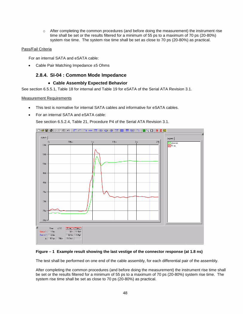
48
o After completing the common procedures (and before doing the measurement) the instrument rise time shall be set or the results filtered for a minimum of 55 ps to a maximum of 70 ps (20-80%) system rise time. The system rise time shall be set as close to 70 ps (20-80%) as practical.
Pass/Fail Criteria
For an internal SATA and eSATA cable:
• Cable Pair Matching Impedance ±5 Ohms
2.8.4. SI-04 : Common Mode Impedance • Cable Assembly Expected Behavior
See section 6.5.5.1, Table 18 for internal and Table 19 for eSATA of the Serial ATA Revision 3.1. Measurement Requirements
• This test is normative for internal SATA cables and informative for eSATA cables.
• For an internal SATA and eSATA cable:
See section 6.5.2.4, Table 21, Procedure P4 of the Serial ATA Revision 3.1.
Figure – 1 Example result showing the last vestige of the connector response (at 1.8 ns) The test shall be performed on one end of the cable assembly, for each differential pair of the assembly. After completing the common procedures (and before doing the measurement) the instrument rise time shall be set or the results filtered for a minimum of 55 ps to a maximum of 70 ps (20-80%) system rise time. The system rise time shall be set as close to 70 ps (20-80%) as practical.
49
Pass/Fail Criteria
For an internal SATA and eSATA cable:
• Common Mode Impedance 25 - 40 Ohms
2.8.5. SI-05 : Differential Rise Time • Cable Assembly Expected Behavior
See section 6.6.1.1, Table 18 for internal and Table 19 for eSATA of the Serial ATA Revision 3.1. Measurement Requirements
• This test is normative for internal SATA cables and eSATA cables.
• For an internal SATA and eSATA cable:
o See section 6.6.2.4, Table 23, Procedure P8 of the Serial ATA Revision 3.1. o The test shall be performed in one direction on the cable assembly, for each differential pair of the
assembly.
Pass/Fail Criteria
For an internal SATA cable:
• Maximum Rise Time 85 ps (20-80%) For an eSATA cable:
• Maximum Rise Time 150 ps (20-80%)
2.8.6. SI-06 : Intra-Pair Skew • Cable Assembly Expected Behavior
See section 6.6.1.1, Table 18 for internal and Table 19 for eSATA of the Serial ATA Revision 3.1. The test shall be performed in one direction on the cable assembly, for each differential pair of the assembly. Measurement Requirements
• See section 6.6.2.4, Table 23, Procedure P10 of the Serial ATA Revision 3.1. • This test is normative for internal SATA cables and for eSATA cables.
• All cables and all adapters shall be de-skewed just prior to performing the measurement. Note that the inclusion of the adapters in calibrations for other tests may not be correct.
Pass/Fail Criteria
For an internal SATA cable • Maximum Intra-Pair Skew 10 ps For an eSATA cable • Maximum Intra-Pair Skew 20 ps
2.8.7. SI-07 : Insertion Loss • Cable Assembly Expected Behavior
See section 6.6.1.1, Table 18 for internal and Table 19 for eSATA of the Serial ATA Revision 3.1.
50
The test shall be performed in one direction on the cable assembly, for each differential pair of the assembly. If a family of cables is being tested, only the longest length is tested for this requirement. Measurement Requirements
• This test is normative for internal SATA cables and for eSATA cables.
• For an internal SATA and eSATA cable:
o See section 6.6.2.4, Table 23, Procedure P5 of the Serial ATA Revision 3.1.
Pass/Fail Criteria For an internal SATA cable:
• Maximum Insertion Loss of Cable (10-4500 MHz) 6 dB For an eSATA cable:
• Maximum Insertion Loss of Cable (10-4500 MHz) 8 dB
2.8.8. SI-08 : Differential to Differential Crosstalk: NEXT • Cable Assembly Expected Behavior
See section 6.6.1.1, Table 18 for internal and Table 19 for eSATA of the Serial ATA Revision 3.1. The test shall be performed on both ends of the cable assembly, but only needs to be measured in one direction on each end (for example, with the Tx pair as the aggressor, and the Rx pair as the receiver). Measurement Requirements
• This test is normative for internal SATA cables and for eSATA cables.
• For an internal SATA and eSATA cable: o See section 6.6.2.4, Table 23 Procedure P6 of the Serial ATA Revision 3.1. o If time-based test equipment is used to measure the NEXT, it shall use an acquisition window that is at
least 4 times the propagation delay of the cable (electrical length). o For test adapters comprising of 2 plugs to SMA and 1 receptacle to SMA adapters, each combination of
plug / receptacle shall have a NEXT performance better than -36 dB (10-4500 MHz). The performance measurement of this adapter combination shall be made and saved on a daily basis, or each time the setup is restored. In the event of a product failure, re-confirm that the adapter performance meets this requirement. For this measurement, the tester is required to continue to follow the same procedure for making a NEXT measurement on a product (see Procedure P6).
Pass/Fail Criteria
For an internal SATA and eSATA cable: • Maximum Crosstalk: NEXT (10-4500 MHz) -26 dB
2.8.9. SI-09 : Inter-Symbol Interference • Cable Assembly Expected Behavior
See section 6.6.1.1, Table 16 of the Serial ATA Revision 3.1. The test shall be performed in one direction on the cable assembly, for each differential pair of the assembly. If a family of cables is being tested, only the longest length is tested for this requirement.
51
Measurement Requirements
• This test is normative for internal SATA cables and for eSATA cables.
• For an internal SATA and eSATA cable: o See section 6.6.2.4, Table 23, Procedure P9 of the Serial ATA Revision 3.1. o As incident (test system induced) DJ may not be de-convolved from the end results, it is critical to use
a high quality (low jitter) fixture and stimulus system when performing this test. o The 20%-80% rise time and fall time of the pattern source shall be 136 ps, or as close to 136 ps as is
practical, to minimize the resulting DJ and produce the most accurate results. Generate a LBP (Lone Bit Pattern) at 3.0 Gbps through the fixture.
Pass/Fail Criteria
For an internal SATA and eSATA cable: • Maximum Inter-Symbol Interference 50 ps
2.9. Mechanical – Device - Standard Internal Connector
2.9.1. MDI-01 : Connector Location • Device Expected Behavior
See section 6.1.2 of the Serial ATA Revision 3.1. See section 6.3 of the Serial ATA Revision 3.1 for slimline ATAPI device requirements. See section 6.2.3 of Serial ATA Revision 3.1 for Micro SATA device requirements. Measurement Requirements
• For a 12.7mm Slimline optical device see section 6.3.3.2, Figure 61 and 64 of the Serial ATA Revision 3.1 Specification.
• For a 9.5 mm Slimline optical device see section 6.3.3.2, Figure 61 and 63 of the Serial ATA Revision 3.1 Specification.
• For a 7mm Slimline optical device see section 6.3.3.2, Figure 60 and 62 of the Serial ATA Revision 3.1 Specification.
• For a 5.25” optical device see section 6.1.2, Figure 20 of the Serial ATA Revision 3.1 Specification. • For a 5.25” non-optical device see section 6.1.2, Figure 21 of the Serial ATA Revision 3.1 Specification. • For a 3.5” side mounted device see section 6.1.2, Figure 22 of the Serial ATA Revision 3.1 Specification. • For a 3.5” bottom mounted device see section 6.1.2, Figure 23 of the Serial ATA Revision 3.1 Specification. • For a 2.5” side mounted device see section 6.1.2, Figure 24 of the Serial ATA Revision 3.1 Specification. • For a 2.5” bottom mounted device see section 6.1.2, Figure 25 of the Serial ATA Revision 3.1 Specification. • For a Micro SATA Connector for 1.8” HDD see section 6.2.3, Figure 52 and Figure 53 of the Serial ATA
Revision 3.1 Specification. • For a device mSATA Card see section 6.5.3.2, Figure 94 and Figure 95 of the Serial ATA Revision 3.1
Specification. Pass/Fail Criteria
• NOTE: all applicable measurements within this test shall be verified as a pass for the overall result of this test requirement to be reported as a PASS.
• For a 12.7 mm Slimline optical device: a) From the bottom surface of the drive to the top of the tongue of the SATA plug. 6.20 +- 0.38 mm b) Parallelism of the top of the tongue of the SATA plug vs. the bottom surface of the drive. 0.40 mm c) From the edge of the drive to the centerline of the SATA plug. 21.25 +- 0.38 mm
52
d) From the back surface of the drive (i.e. the “end of the device factor”) to the base of the tongue of the SATA plug. 5.20 +- 0.3 mm
• For a 9.5 mm Slimline optical device: a) From the bottom surface of the drive to the top of the tongue of the SATA plug. 6.00 +- 0.38 mm b) Parallelism of the top of the tongue of the SATA plug vs. the bottom surface of the drive. 0.40 mm c) From the edge of the drive to the centerline of the SATA plug. 21.25 +- 0.38 mm d) From the back surface of the drive (i.e. the “end of the device factor”) to the base of the tongue of the SATA plug. 5.20 +- 0.3 mm
• For a 7mm Slimline optical device: a) From the bottom surface of the drive to the top of the tongue of the SATA plug 5.1 +- 0.38 b) Parallelism of the top of the tongue of the SATA plug vs. the bottom surface of the drive.
0.40 mm c) From the edge of the drive to the centerline of the SATA plug.
21.25 +- 0.38 mm d) From the back surface of the drive (i.e. the “end of the device factor”) to the base of the tongue of the
SATA plug. 5.20 +- 0.3 mm • For a 5.25” optical device:
a) From the bottom surface of the drive to the top of the tongue of the SATA plug. 10.00 +- 0.38 mm b) Parallelism of the top of the tongue of the SATA plug vs. the bottom surface of the drive. 0.40 mm c) From the centerline of the drive to the centerline of the SATA plug. 25.00 +- 0.38 mm d) From the back surface of the drive (i.e. the “end of the device factor”) to the base of the tongue of the SATA plug. 4.90 +- 0.50 mm
• For a 5.25” non-optical device: If the device follows section 6.1.2, Figure 20 then use the Pass/Fail criteria for a “5.25” optical drive”. If the device does not follow section 6.1.2, Figure 20 then:
a) From the bottom surface of the drive to the top of the tongue of the SATA plug. 3.50 +- 0.38 mm b) Parallelism of the top of the tongue of the SATA plug vs. the bottom surface of the drive. 0.40 mm c) From the centerline of the drive to the centerline of the SATA plug. 42.90 +- 0.38 mm d) From the back surface of the drive (i.e. the “end of the device factor”) to the base of the tongue of the SATA plug. 4.90 +- 0.50 mm
• For a 3.5” device: a1) From the centerline of the side mounting holes to the top of the tongue of the SATA plug. 2.85 +- 0.38 mm a2) From the bottom surface of the drive to the top of the tongue of the SATA plug. 3.50 +- 0.38 mm b) Parallelism of the top of the tongue of the SATA plug vs. the bottom surface of the drive. 0.25 mm c) From the centerline of the drive to the centerline of the SATA plug. 20.68 +- 0.38 mm d1) From the centerline of the side mounting holes to the base of the tongue of the SATA plug. 23.60 +- 0.50 mm d2) From the centerline of the bottom mounting holes to the base of the tongue of the SATA plug. 36.38 +- 0.50 mm
• For a 2.5” device:
53
a1) From the centerline of the side mounting holes to the top of the tongue of the SATA plug. 0.50 +- 0.38 mm a2) From the bottom surface of the drive to the top of the tongue of the SATA plug. 3.50 +- 0.38 mm b) Parallelism of the top of the tongue of the SATA plug vs. the bottom surface of the drive. 0.25 mm c) From the centerline of the drive to the centerline of the SATA plug. 4.80 +- 0.38 mm d1) From the centerline of the side mounting holes to the base of the tongue of the SATA plug. 9.40 +- 0.50 mm d2) From the centerline of the bottom mounting holes to the base of the tongue of the SATA plug. 9.40 +- 0.50 mm
For a Micro SATA Connector for 1.8” HDD: a) From the bottom surface of the drive to the top of the tongue shall be 78.5 +/- 0.3 mm. b) Parallelism of the top of the tongue of the SATA plug vs. the top surface of the drive shall be 0.40 mm
maximum. c) From the centerline of the drive to the centerline of the SATA plug shall be 0.0 +/- 0.20 mm. d) From the back surface of the drive (i.e. the “end of the device factor”) to the base of the tongue of the
SATA plug shall be 4.9 mm +/- 0.08 mm. e) The Thickness of both sides of the drive shall be 3.30 +/- 0.2 mm.
For a device mSATA Card :
a) From the top of the connector to the end of the device shall be 50.8 +/- *** mm. b) The width of the device shall be 29.50 +/- *** mm. c) From the centerline of the drive to the centerline of the Pin15 and Pin 17 shall be 3.85 +/- *** mm. d) Depth of tongue (from top to base) shall be 3.20mm MIN e) mSATA connector gap shall be 1.50mm +/- 0.10mm
*** No tolerance in Serial ATA Revision 3.1
2.9.2. MDI-02 : Visual and Dimensional Inspections • Device Expected Behavior
See section 6.1.10.2, Table 6 of the Serial ATA Revision 3.1. See section 6.3 of the Serial ATA Revision 3.1 for slimline ATAPI device requirements. See section 6.2.4 of the Serial ATA Revision 3.1 for Micro SATA device requirements. Measurement Requirements
• For Slimline optical device see section 6.3.4.1, Figures 65, 66, 67, 68, and 69of the Serial ATA Revision 3.1 Specification.
• For Micro SATA HDDs see section 6.2.4, Figure 56 of the Serial ATA Revision 3.1. • For all other devices, see section 6.1.10.2, Table 6; section 6.1.2, Figure 26; and section 6.1.3.1, Figures 27
and 28 of the Serial ATA Revision 3.1. Pass/Fail Criteria
• NOTE: all applicable measurements within this test shall be verified as a pass for the overall result of this test requirement to be reported as a PASS.
For Slimline devices a) The thickness of the device plug tongue shall be 1.23 +- 0.05 mm (Figure 71, section A-A). b) If the “Optional Wall” of Figure 71 is present then the distance from the device plug tongue to the wall shall be 1.58 +- 0.08 mm (Figure 71, section A-A). c) If the “Optional Wall” of Figure 71 is not present then there shall be a minimum of a 1.50 mm keep out zone from Datum A of Figure 5 to the nearest obstruction. d) The combined width of the power and signal segments shall be 20.4 +- 0.08 mm (Figure 70). e) The separation between the power and signal segments shall be 2.34 +- 0.05 mm (Figure 70).
For Micro SATA devices:
54
a) The thickness of the device plug tongue shall be 1.23 +/- 0.05 mm (Figure 56, section C-C). b) The combined width of the power and signal segments shall be 27.04 +/- 0.06 mm (Figure 56) c) The separation between the power and signal segments shall be 2.41 +/- 0.05 mm (Figure 56)
For all other devices: a) The thickness of the device plug tongue shall be 1.23 +- 0.05 mm (Figure 30, section C-C). b) If the “Optional Wall” of Figure 30 is present then the distance from the device plug tongue to the wall shall be 1.58 +- 0.08 mm (Figure 30, section B-B). c) If the “Optional Wall” of Figure 30 is not present then there shall be a minimum of a 1.5 mm keep out zone from Datum A of Figure 28 to the nearest obstruction. d) The combined width of the power and signal segments shall be 33.39 +- 0.08 mm (Figure 29). e) The separation between the power and signal segments shall be 2.41 +- 0.05 mm (Figure 29).
2.10. Mechanical – Device - Power Connector
2.10.1. MDP-01 : Visual and Dimensional Inspections • Device Expected Behavior
See section 6.1.10.2, Table 6 of the Serial ATA Revision 3.1. See section 6.3 of the Serial ATA Revision 3.1 for slimline ATAPI device requirements. See section 6.2.4 of the Serial ATA Revision 3.1 for Micro SATA device requirements. Measurement Requirements
• For a Slimline optical device see section 6.3.4.2, Figure 70of the Serial ATA Revision 3.1 • For Micro SATA devices see section 6.2.4, Figure 56 of the Serial ATA Revision 3.1. • For all other devices, see section 6.1.10.2, Table 6; section 6.1.2, Figure 26; and section 6.1.3.1, Figures 27
and 28 of the Serial ATA Revision 3.1. Pass/Fail Criteria
• NOTE: all applicable measurements within this test shall be verified as a pass for the overall result of this test requirement to be reported as a PASS.
For Slimline devices: a) The thickness of the device plug tongue shall be 1.23 +- 0.05 mm (Figure 71, section A-A). b) If the “Optional Wall” of Figure 71 is present then the distance from the device plug tongue to the wall shall be 1.58 +- 0.08 mm (Figure 71, section A-A). c) If the “Optional Wall” of Figure 71 is not present then there shall be a minimum of a 1.5 mm keep out zone from Datum A of Figure 71 to the nearest obstruction.
For Micro SATA devices: a) The thickness of the device plug tongue shall be 1.23 +/- 0.05 mm (Figure 56, section C-C).
For all other devices: a) The thickness of the device plug tongue shall be 1.23 +- 0.05 mm (Figure 30, section C-C). b) If the “Optional Wall” of Figure 30 is present then the distance from the device plug tongue to the wall shall be 1.58 +- 0.08 mm (Figure 30, section B-B). c) If the “Optional Wall” of Figure 30 is not present then there shall be a minimum of a 1.5 mm keep out zone from Datum A of Figure 28 to the nearest obstruction.
2.11. Mechanical – Host - Standard Internal Connector
2.11.1. MHI-01 : Visual and Dimensional Inspections (Informative) • Host Assembly Expected Behavior
See section 6.3 of the Serial ATA Revision 3.1 . Measurement Requirements
55
• For a Slimline host, see section 6.3.4.3, Figure 81 of the Serial ATA Revision 3.1. • For all other hosts, see section 6.1.5, Figure 34 of the Serial ATA Revision 3.1.
Pass/Fail Criteria
• NOTE: all applicable measurements within this test shall be verified as a pass for the overall result of this test requirement to be reported as a PASS.
For Slimline hosts: a) Inside width of Slimline Host Receptacle Connector shall be 20.6 +- 0.10 mm. b) Width of key between power and signal segment shall be 2.04 +-0.10 mm. c) Outside with of Slimline Host Receptacle Connector shall be 25.4 +- 0.15 mm. For all other hosts: a) Gap between tongue to edge of blind mate key shall be 1.65 +- 0.15 mm b) Gap between tongue to blind mate key shall be 3.05 +- 0.08 mm c) Gap between tongue and 2nd wall shall be a minimum of 1.10 mm d) Width of tongue shall be 10.41 +- 0.08 mm e) Width of short leg of "L" shall be 1.15 +- 0.05 mm f) Depth of tongue (from tip to base) shall be 5.40 +- 0.08 g) Inside width of the blind mate key shall be 2.20 +- 0.15 mm h) Thickness of tongue shall be 1.23 +- 0.05 mm i) Gap between tongue and keep out or optional latching wall shall be 1.58 +- 0.08 mm Mechanical – Drive/Host – Standard External Connector Requirements
2.12. Mechanical – Drive/Host – eSATA Connector (informative)
2.12.1. MXE-01 : Visual and Dimension Inspection • Expected Behavior
See overview and references to Serial ATA Revision 3.1.
Measurement Requirements • See section 6.7.1, Figure 105 - 110 of the Serial ATA Revision 3.1. • Figure 05 through 110specified mechanical dimensions of external RA SMT plug, RA SMT plug- reversed pin
out, RA through-hole plug, vertical SMT plug and vertical through-hole plug respectively. The following Pass/Fail criteria uses RA SMT plug (Figure 105) as an example. Other types of plugs (Figure 106 - 110) shall follow the same criteria accordingly.
Pass/Fail Criteria All applicable parts shall pass for the test to pass:
a) The height of the slot in RA SMT plug shall be 4.10 +/- 0.1 (Figure 106 - 110) b) The height of the slot (for receptacle key) shall be 1.50 +/- 0.08 (Figure 106 - 110) c) The thickness of the plug tongue shall be 1.20 +/- 0.05 (Figure 106 - 110) d) The width of the plug tongue shall be 10.00 +/- 0.05 (Figure 106 - 110) e) The width of the slot (for receptacle key) shall be 15.00 +/- 0.05 (Figure 106 - 110) f) The width of the bottom slot (for receptacle wall) shall be 13.00 +/- 0.05 (Figure 106 - 110) g) The width of the top slot (for receptacle) shall be 10.00 +/- 0.05 (Figure 106 - 110) h) The retention springs (x4) of the plug connector shall have the spring tip aligned with the datum (Y) within 4.10 +/-
0.1 (Figure 106 - 110) i) Informative - The retention springs (x4) of the plug connector shall have width 1.50+/- 0.1 (Figure 106 - 110) j) Informative - The retention springs (x4) of the plug connector shall be bilaterally located with the centerline within
6.80 +/- 0.1 (Figure 106 - 110) k) Informative - The length of the contact blades shall be 4.25 +/- 0.1 for each of the 4 signal pins and 4.75 +/- 0.1 for
each of the 3 ground pins as measured from datum plane Y (Figure 106 - 110).
56
2.13. Phy General Requirements
2.13.1. PHY-01 : Unit Interval • Device/Host Expected Behavior
See section 7.2.2.1.3 of Serial ATA Revision 3.1. Measurement Requirements
• See section 7.4.15 of Serial ATA Revision 3.1. • For products which support 6 Gbps, this requirement shall be tested at all interface rates (1.5 Gbps, 3 Gbps
and 6 Gbps). In general all interface rates claimed to be supported by the PUT shall be tested. Pass/Fail Criteria
• PHY-01a - Mean Unit Interval measured between 666.4333 ps (min) to 670.2333 ps (max) (for products running at 1.5 Gbps)
• PHY-01b - Mean Unit Interval measured between 333.2167 ps (min) to 335.1167 ps (max) (for products running at 3 Gbps)
• PHY-01c – Mean Unit Interval measured between 166.6083 ps (min) to 167.5583 ps (max) (for products running at 6 Gbps)
• The values above shall be based on at least 100,000 UIs (covers at least one SSC profile)
2.13.2. PHY-02 : Frequency Long Term Stability • Device/Host Expected Behavior
This test is not applicable to products that support SSC. See section 7.2.2.1.4 of Serial ATA Revision 3.1. Measurement Requirements
• See section 7.4.7 of Serial ATA Revision 3.1. • This test is only run once at the maximum interface rate of the product (1.5 Gbps, 3 Gbps or 6 Gbps). • The execution of this test shall include use of the frequency demodulator and low pass filter defined within
section 7.4.15 of Serial ATA Revision 3.1. Pass/Fail Criteria
• ftol measured between -350ppm and 350ppm
2.13.3. PHY-03 : Spread-Spectrum Modulation Frequency • Device/Host Expected Behavior
See sections 7.2.2.1.5 and 7.3.3 of Serial ATA Revision 3.1. This test requires support for Spread Spectrum Clocking (SSC), which is optional. Measurement Requirements
• See section 7.4.15 of Serial ATA Revision 3.1. • This test is only run once at the maximum interface rate of the product (1.5 Gbps, 3 Gbps or 6 Gbps).
Pass/Fail Criteria
• fSSC measured between 30 kHz and 33 kHz • The value above shall be based on a mean of at least 10 complete SSC cycles
57
2.13.4. PHY-04 : Spread-Spectrum Modulation Deviation • Device/Host Expected Behavior
See sections 7.2.2.1.6 and 7.3.3 of Serial ATA Revision 3.1. This test requires support for Spread Spectrum Clocking (SSC), which is optional. Measurement Requirements
• See section 7.4.15 of Serial ATA Revision 3.1. • This test is only run once at the maximum interface rate of the product (1.5 Gbps, 3 Gbps or 6 Gbps). • The value reported as the result shall be the single total range value relative to nominal of the SSC
modulation deviation, using the equations below, where “Min” is the mean of 10 recorded values of the minimum peaks and “Max: is the mean of 10 recorded values of the maximum peaks.
• Calculate max deviation = (Measured Max – Nominal)/Nominal * 1e6 ppm • Calculate min deviation = (Measured Min – Nominal)/Nominal * 1e6 ppm
Pass/Fail Criteria
a) Max SSCtol measured (using mean of 10 recorded values) less than +350ppm. b) Min SSCtol measured (using mean of 10 recorded values) greater than -5350ppm.
2.14. Phy Transmitter Requirements During the testing execution for all TX test requirements, it is essential that the product under test be able to complete an initial OOB sequence through the device COMWAKE. This is to allow product calibration to occur prior to and/or during the initial power on and detect sequences.
2.14.1. TX-01 : Pair Differential Impedance(Informative) • Device/Host Expected Behavior
See sections 7.2.2.2.1 of Serial ATA Revision 3.1. Measurement Requirements
• See section 7.4.27 of Serial ATA Revision 3.1 • . This test requirement is only applicable to products running at 1.5 Gbps. For products which support 3 Gbps
or 6 Gbps, this test is not required. • Testing of this requirement shall be completed during transmission of the Mid Frequency Test Pattern
(MFTP), The amplitude of a TDR pulse or excitation applied to an active transmitter shall not exceed 139 mVpp (-13.2 dBm 50 Ohms) single ended.
Pass/Fail Criteria
• Verify that both the minimum [TX-01a] and maximum [TX-01b] results for the pair differential impedance measured between 85 Ohms and 115 Ohms (for products running at 1.5 Gbps)
• NOTE: The verification of this result may not be required. If a product which supports 1.5 Gbps product passes TX-06, then it is not required that this test be verified. This result shall be verified for a 1.5 Gbps product if it fails TX-06.
2.14.2. TX-02 : Single-Ended Impedance (Obsolete) • Device/Host Expected Behavior
See section 7.2.2.2.2 of Serial ATA Revision 3.1. Measurement Requirements
• See section 7.4.28 of Serial ATA Revision 3.1. • This test requirement is only applicable to products that support a maximum operating speed of 1.5 Gbps.
For products that support a maximum operating speed of 3.0 Gbps or 6.0 Gbps this test is not required.
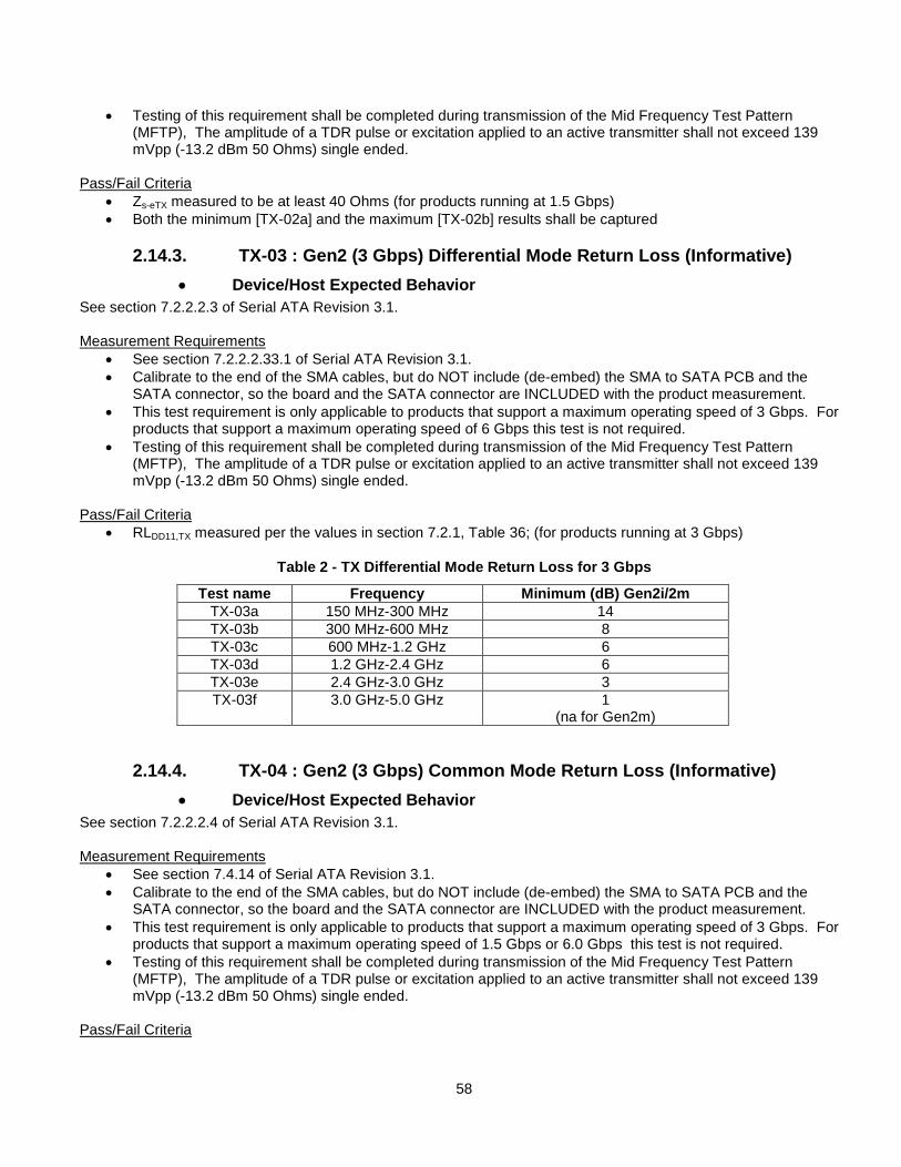
58
• Testing of this requirement shall be completed during transmission of the Mid Frequency Test Pattern (MFTP), The amplitude of a TDR pulse or excitation applied to an active transmitter shall not exceed 139 mVpp (-13.2 dBm 50 Ohms) single ended.
Pass/Fail Criteria
• Zs-eTX measured to be at least 40 Ohms (for products running at 1.5 Gbps) • Both the minimum [TX-02a] and the maximum [TX-02b] results shall be captured
2.14.3. TX-03 : Gen2 (3 Gbps) Differential Mode Return Loss (Informative) • Device/Host Expected Behavior
See section 7.2.2.2.3 of Serial ATA Revision 3.1. Measurement Requirements
• See section 7.2.2.2.33.1 of Serial ATA Revision 3.1. • Calibrate to the end of the SMA cables, but do NOT include (de-embed) the SMA to SATA PCB and the
SATA connector, so the board and the SATA connector are INCLUDED with the product measurement. • This test requirement is only applicable to products that support a maximum operating speed of 3 Gbps. For
products that support a maximum operating speed of 6 Gbps this test is not required. • Testing of this requirement shall be completed during transmission of the Mid Frequency Test Pattern
(MFTP), The amplitude of a TDR pulse or excitation applied to an active transmitter shall not exceed 139 mVpp (-13.2 dBm 50 Ohms) single ended.
Pass/Fail Criteria
• RLDD11,TX measured per the values in section 7.2.1, Table 36; (for products running at 3 Gbps)
Table 2 - TX Differential Mode Return Loss for 3 Gbps
Test name Frequency Minimum (dB) Gen2i/2m TX-03a 150 MHz-300 MHz 14 TX-03b 300 MHz-600 MHz 8 TX-03c 600 MHz-1.2 GHz 6 TX-03d 1.2 GHz-2.4 GHz 6 TX-03e 2.4 GHz-3.0 GHz 3 TX-03f 3.0 GHz-5.0 GHz 1
(na for Gen2m)
2.14.4. TX-04 : Gen2 (3 Gbps) Common Mode Return Loss (Informative) • Device/Host Expected Behavior
See section 7.2.2.2.4 of Serial ATA Revision 3.1. Measurement Requirements
• See section 7.4.14 of Serial ATA Revision 3.1. • Calibrate to the end of the SMA cables, but do NOT include (de-embed) the SMA to SATA PCB and the
SATA connector, so the board and the SATA connector are INCLUDED with the product measurement. • This test requirement is only applicable to products that support a maximum operating speed of 3 Gbps. For
products that support a maximum operating speed of 1.5 Gbps or 6.0 Gbps this test is not required. • Testing of this requirement shall be completed during transmission of the Mid Frequency Test Pattern
(MFTP), The amplitude of a TDR pulse or excitation applied to an active transmitter shall not exceed 139 mVpp (-13.2 dBm 50 Ohms) single ended.
Pass/Fail Criteria
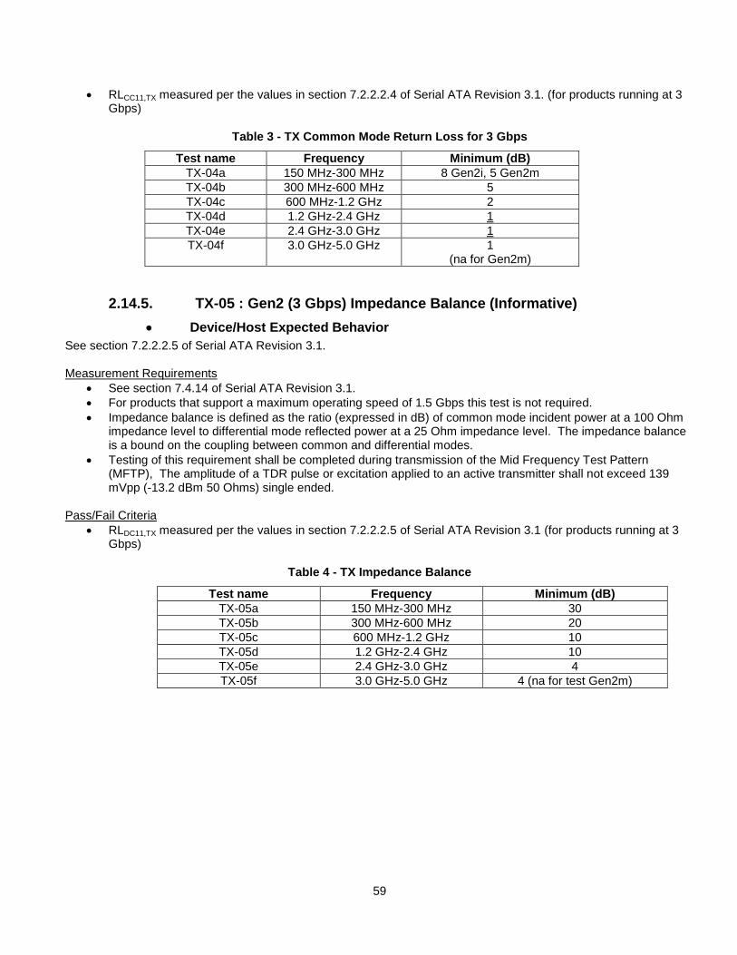
59
• RLCC11,TX measured per the values in section 7.2.2.2.4 of Serial ATA Revision 3.1. (for products running at 3 Gbps)
Table 3 - TX Common Mode Return Loss for 3 Gbps
Test name Frequency Minimum (dB) TX-04a 150 MHz-300 MHz 8 Gen2i, 5 Gen2m TX-04b 300 MHz-600 MHz 5 TX-04c 600 MHz-1.2 GHz 2 TX-04d 1.2 GHz-2.4 GHz 1 TX-04e 2.4 GHz-3.0 GHz 1 TX-04f 3.0 GHz-5.0 GHz 1
(na for Gen2m)
2.14.5. TX-05 : Gen2 (3 Gbps) Impedance Balance (Informative) • Device/Host Expected Behavior
See section 7.2.2.2.5 of Serial ATA Revision 3.1. Measurement Requirements
• See section 7.4.14 of Serial ATA Revision 3.1. • For products that support a maximum operating speed of 1.5 Gbps this test is not required. • Impedance balance is defined as the ratio (expressed in dB) of common mode incident power at a 100 Ohm
impedance level to differential mode reflected power at a 25 Ohm impedance level. The impedance balance is a bound on the coupling between common and differential modes.
• Testing of this requirement shall be completed during transmission of the Mid Frequency Test Pattern (MFTP), The amplitude of a TDR pulse or excitation applied to an active transmitter shall not exceed 139 mVpp (-13.2 dBm 50 Ohms) single ended.
Pass/Fail Criteria
• RLDC11,TX measured per the values in section 7.2.2.2.5 of Serial ATA Revision 3.1 (for products running at 3 Gbps)
Table 4 - TX Impedance Balance
Test name Frequency Minimum (dB) TX-05a 150 MHz-300 MHz 30 TX-05b 300 MHz-600 MHz 20 TX-05c 600 MHz-1.2 GHz 10 TX-05d 1.2 GHz-2.4 GHz 10 TX-05e 2.4 GHz-3.0 GHz 4 TX-05f 3.0 GHz-5.0 GHz 4 (na for test Gen2m)
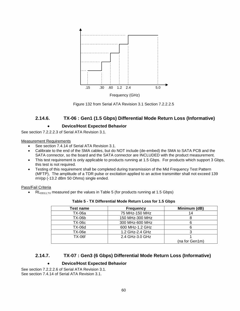
60
Frequency (GHz)
.15 .30 .60 1.2 2.4 5.0
Figure 132 from Serial ATA Revision 3.1 Section 7.2.2.2.5
2.14.6. TX-06 : Gen1 (1.5 Gbps) Differential Mode Return Loss (Informative) • Device/Host Expected Behavior
See section 7.2.2.2.3 of Serial ATA Revision 3.1. Measurement Requirements
• See section 7.4.14 of Serial ATA Revision 3.1. • Calibrate to the end of the SMA cables, but do NOT include (de-embed) the SMA to SATA PCB and the
SATA connector, so the board and the SATA connector are INCLUDED with the product measurement. • This test requirement is only applicable to products running at 1.5 Gbps. For products which support 3 Gbps,
this test is not required. • Testing of this requirement shall be completed during transmission of the Mid Frequency Test Pattern
(MFTP), The amplitude of a TDR pulse or excitation applied to an active transmitter shall not exceed 139 mVpp (-13.2 dBm 50 Ohms) single ended.
Pass/Fail Criteria
• RLDD11,TX measured per the values in Table 5 (for products running at 1.5 Gbps)
Table 5 - TX Differential Mode Return Loss for 1.5 Gbps
Test name Frequency Minimum (dB) TX-06a 75 MHz-150 MHz 14 TX-06b 150 MHz-300 MHz 8 TX-06c 300 MHz-600 MHz 6 TX-06d 600 MHz-1.2 GHz 6 TX-06e 1.2 GHz-2.4 GHz 3 TX-06f 2.4 GHz-3.0 GHz 1
(na for Gen1m)
2.14.7. TX-07 : Gen3 (6 Gbps) Differential Mode Return Loss (Informative) • Device/Host Expected Behavior
See section 7.2.2.2.6 of Serial ATA Revision 3.1. See section 7.4.14 of Serial ATA Revision 3.1.
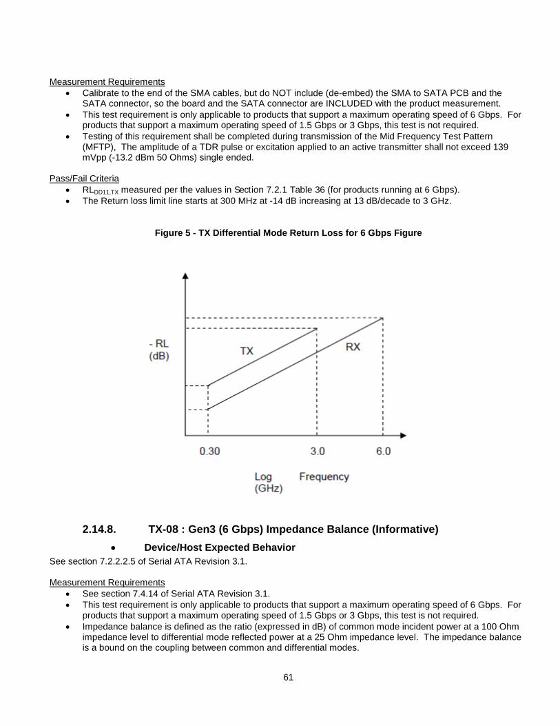
61
Measurement Requirements
• Calibrate to the end of the SMA cables, but do NOT include (de-embed) the SMA to SATA PCB and the SATA connector, so the board and the SATA connector are INCLUDED with the product measurement.
• This test requirement is only applicable to products that support a maximum operating speed of 6 Gbps. For products that support a maximum operating speed of 1.5 Gbps or 3 Gbps, this test is not required.
• Testing of this requirement shall be completed during transmission of the Mid Frequency Test Pattern (MFTP), The amplitude of a TDR pulse or excitation applied to an active transmitter shall not exceed 139 mVpp (-13.2 dBm 50 Ohms) single ended.
Pass/Fail Criteria
• RLDD11,TX measured per the values in Section 7.2.1 Table 36 (for products running at 6 Gbps). • The Return loss limit line starts at 300 MHz at -14 dB increasing at 13 dB/decade to 3 GHz.
Figure 5 - TX Differential Mode Return Loss for 6 Gbps Figure
2.14.8. TX-08 : Gen3 (6 Gbps) Impedance Balance (Informative) • Device/Host Expected Behavior
See section 7.2.2.2.5 of Serial ATA Revision 3.1. Measurement Requirements
• See section 7.4.14 of Serial ATA Revision 3.1. • This test requirement is only applicable to products that support a maximum operating speed of 6 Gbps. For
products that support a maximum operating speed of 1.5 Gbps or 3 Gbps, this test is not required. • Impedance balance is defined as the ratio (expressed in dB) of common mode incident power at a 100 Ohm
impedance level to differential mode reflected power at a 25 Ohm impedance level. The impedance balance is a bound on the coupling between common and differential modes.
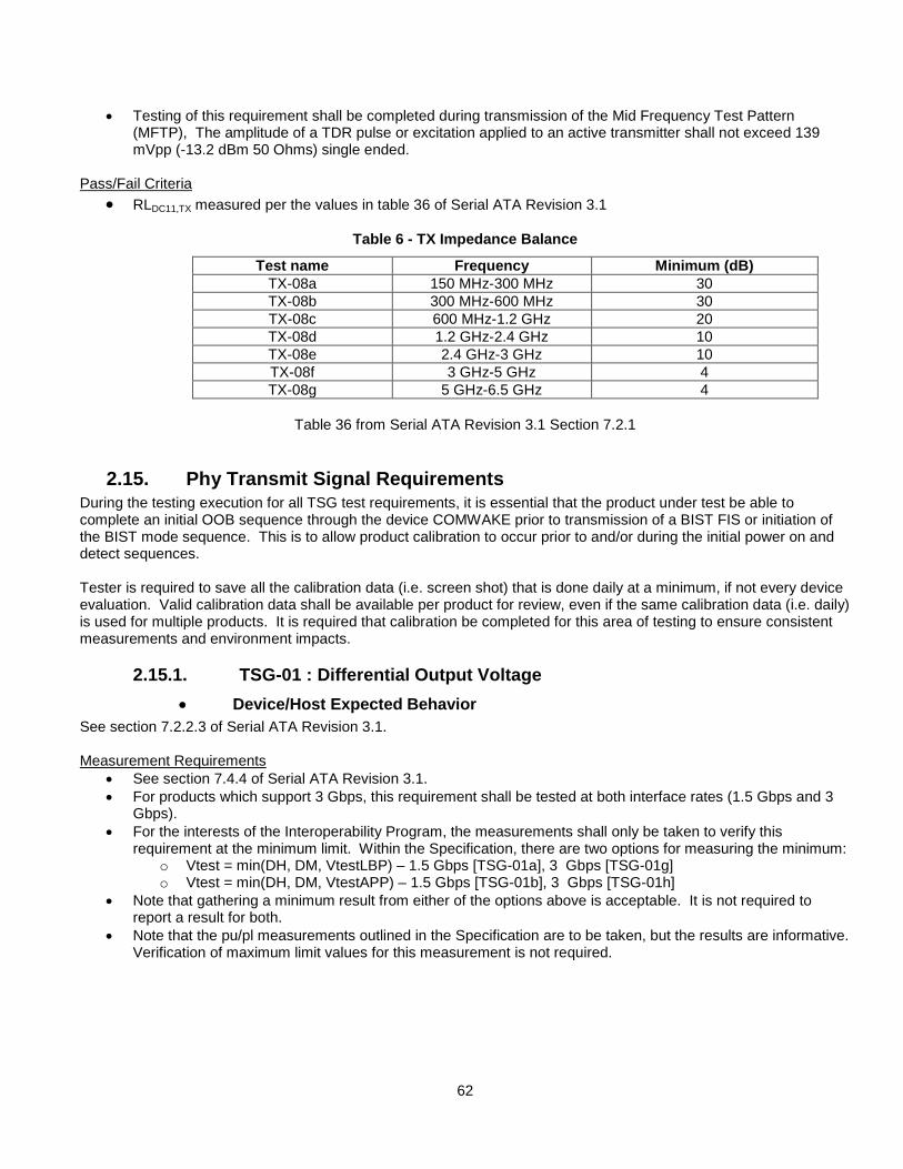
62
• Testing of this requirement shall be completed during transmission of the Mid Frequency Test Pattern (MFTP), The amplitude of a TDR pulse or excitation applied to an active transmitter shall not exceed 139 mVpp (-13.2 dBm 50 Ohms) single ended.
Pass/Fail Criteria
• RLDC11,TX measured per the values in table 36 of Serial ATA Revision 3.1
Table 6 - TX Impedance Balance
Test name Frequency Minimum (dB) TX-08a 150 MHz-300 MHz 30 TX-08b 300 MHz-600 MHz 30 TX-08c 600 MHz-1.2 GHz 20 TX-08d 1.2 GHz-2.4 GHz 10 TX-08e 2.4 GHz-3 GHz 10 TX-08f 3 GHz-5 GHz 4 TX-08g 5 GHz-6.5 GHz 4
Table 36 from Serial ATA Revision 3.1 Section 7.2.1
2.15. Phy Transmit Signal Requirements During the testing execution for all TSG test requirements, it is essential that the product under test be able to complete an initial OOB sequence through the device COMWAKE prior to transmission of a BIST FIS or initiation of the BIST mode sequence. This is to allow product calibration to occur prior to and/or during the initial power on and detect sequences. Tester is required to save all the calibration data (i.e. screen shot) that is done daily at a minimum, if not every device evaluation. Valid calibration data shall be available per product for review, even if the same calibration data (i.e. daily) is used for multiple products. It is required that calibration be completed for this area of testing to ensure consistent measurements and environment impacts.
2.15.1. TSG-01 : Differential Output Voltage • Device/Host Expected Behavior
See section 7.2.2.3 of Serial ATA Revision 3.1. Measurement Requirements
• See section 7.4.4 of Serial ATA Revision 3.1. • For products which support 3 Gbps, this requirement shall be tested at both interface rates (1.5 Gbps and 3
Gbps). • For the interests of the Interoperability Program, the measurements shall only be taken to verify this
requirement at the minimum limit. Within the Specification, there are two options for measuring the minimum: o Vtest = min(DH, DM, VtestLBP) – 1.5 Gbps [TSG-01a], 3 Gbps [TSG-01g] o Vtest = min(DH, DM, VtestAPP) – 1.5 Gbps [TSG-01b], 3 Gbps [TSG-01h]
• Note that gathering a minimum result from either of the options above is acceptable. It is not required to report a result for both.
• Note that the pu/pl measurements outlined in the Specification are to be taken, but the results are informative. Verification of maximum limit values for this measurement is not required.
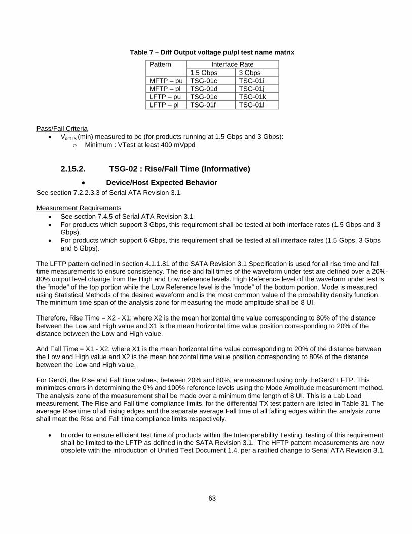
63
Table 7 – Diff Output voltage pu/pl test name matrix
Pattern Interface Rate 1.5 Gbps 3 Gbps
MFTP – pu TSG-01c TSG-01i MFTP – pl TSG-01d TSG-01j LFTP – pu TSG-01e TSG-01k LFTP – pl TSG-01f TSG-01l
Pass/Fail Criteria
• VdiffTX (min) measured to be (for products running at 1.5 Gbps and 3 Gbps): o Minimum : VTest at least 400 mVppd
2.15.2. TSG-02 : Rise/Fall Time (Informative) • Device/Host Expected Behavior
See section 7.2.2.3.3 of Serial ATA Revision 3.1. Measurement Requirements
• See section 7.4.5 of Serial ATA Revision 3.1 • For products which support 3 Gbps, this requirement shall be tested at both interface rates (1.5 Gbps and 3
Gbps). • For products which support 6 Gbps, this requirement shall be tested at all interface rates (1.5 Gbps, 3 Gbps
and 6 Gbps). The LFTP pattern defined in section 4.1.1.81 of the SATA Revision 3.1 Specification is used for all rise time and fall time measurements to ensure consistency. The rise and fall times of the waveform under test are defined over a 20%-80% output level change from the High and Low reference levels. High Reference level of the waveform under test is the “mode” of the top portion while the Low Reference level is the “mode” of the bottom portion. Mode is measured using Statistical Methods of the desired waveform and is the most common value of the probability density function. The minimum time span of the analysis zone for measuring the mode amplitude shall be 8 UI. Therefore, Rise Time = X2 - X1; where X2 is the mean horizontal time value corresponding to 80% of the distance between the Low and High value and X1 is the mean horizontal time value position corresponding to 20% of the distance between the Low and High value. And Fall Time = X1 - X2; where X1 is the mean horizontal time value corresponding to 20% of the distance between the Low and High value and X2 is the mean horizontal time value position corresponding to 80% of the distance between the Low and High value. For Gen3i, the Rise and Fall time values, between 20% and 80%, are measured using only theGen3 LFTP. This minimizes errors in determining the 0% and 100% reference levels using the Mode Amplitude measurement method. The analysis zone of the measurement shall be made over a minimum time length of 8 UI. This is a Lab Load measurement. The Rise and Fall time compliance limits, for the differential TX test pattern are listed in Table 31. The average Rise time of all rising edges and the separate average Fall time of all falling edges within the analysis zone shall meet the Rise and Fall time compliance limits respectively.
• In order to ensure efficient test time of products within the Interoperability Testing, testing of this requirement shall be limited to the LFTP as defined in the SATA Revision 3.1. The HFTP pattern measurements are now obsolete with the introduction of Unified Test Document 1.4, per a ratified change to Serial ATA Revision 3.1.
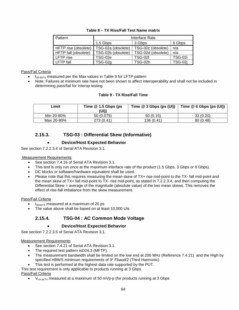
64
Table 8 – TX Rise/Fall Test Name matrix
Pattern Interface Rate 1.5 Gbps 3 Gbps 6 Gbps
HFTP rise (obsolete) TSG-02a (obsolete) TSG-02c (obsolete) n/a HFTP fall (obsolete) TSG-02b (obsolete) TSG-02d (obsolete) n/a LFTP rise TSG-02e TSG-02f TSG-02i LFTP fall TSG-02g TSG-02h TSG-02j
Pass/Fail Criteria
• t20-80TX measured per the Max values in Table 9 for LFTP pattern • Note: Failures at minimum rate have not been shown to affect interoperability and shall not be included in
determining pass/fail for Interop testing
Table 9 - TX Rise/Fall Time
Limit Time @ 1.5 Gbps (ps
(UI)) Time @ 3 Gbps (ps (UI)) Time @ 6 Gbps (ps (UI))
Min 20-80% 50 (0.075) 50 (0.15) 33 (0.20) Max 20-80% 273 (0.41) 136 (0.41) 80 (0.48)
2.15.3. TSG-03 : Differential Skew (Informative) • Device/Host Expected Behavior
See section 7.2.2.3.4 of Serial ATA Revision 3.1. Measurement Requirements
• See section 7.4.16 of Serial ATA Revision 3.1. • This test is only run once at the maximum interface rate of the product (1.5 Gbps, 3 Gbps or 6 Gbps). • DC blocks or software/hardware equivalent shall be used. • Please note that this requires measuring the mean skew of TX+ rise mid-point to the TX- fall mid-point and
the mean skew of TX+ fall mid-point to TX- rise mid-point, as stated in 7.2.2.3.4, and then computing the Differential Skew = average of the magnitude (absolute value) of the two mean skews. This removes the effect of rise-fall imbalance from the skew measurement.
Pass/Fail Criteria
• tskewTX measured at a maximum of 20 ps • The value above shall be based on at least 10,000 UIs
2.15.4. TSG-04 : AC Common Mode Voltage • Device/Host Expected Behavior
See section 7.2.2.3.5 of Serial ATA Revision 3.1. Measurement Requirements
• See section 7.4.21 of Serial ATA Revision 3.1. • The required test pattern isD24.3 (MFTP). • The measurement bandwidth shall be limited on the low end at 200 MHz (Reference 7.4.21) and the High by
specified HBWS minimum requirements of 3* Fbaud/2 (Third Harmonic) • This test is performed at the highest data rate supported by the PUT.
This test requirement is only applicable to products running at 3 Gbps Pass/Fail Criteria
• Vcm,acTX measured at a maximum of 50 mVp-p (for products running at 3 Gbps
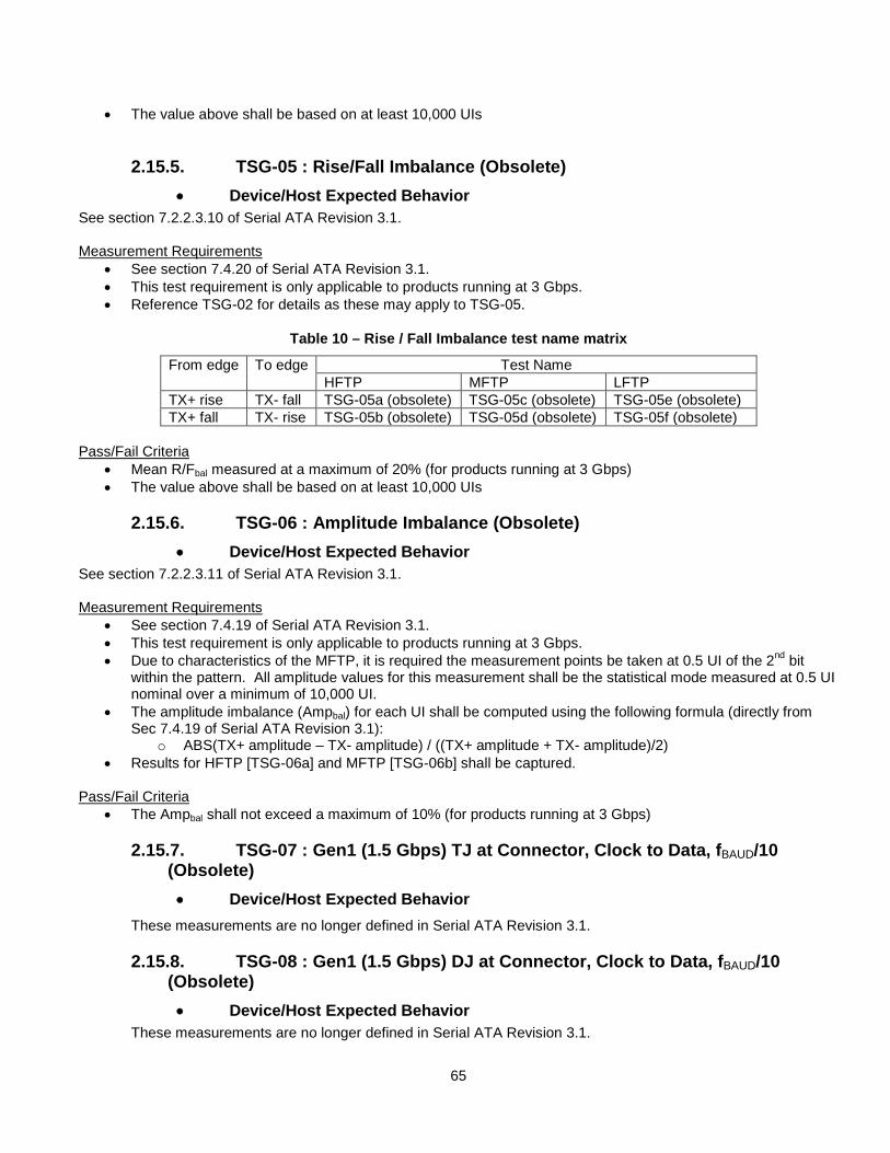
65
• The value above shall be based on at least 10,000 UIs
2.15.5. TSG-05 : Rise/Fall Imbalance (Obsolete) • Device/Host Expected Behavior
See section 7.2.2.3.10 of Serial ATA Revision 3.1. Measurement Requirements
• See section 7.4.20 of Serial ATA Revision 3.1. • This test requirement is only applicable to products running at 3 Gbps. • Reference TSG-02 for details as these may apply to TSG-05.
Table 10 – Rise / Fall Imbalance test name matrix
From edge To edge Test Name HFTP MFTP LFTP
TX+ rise TX- fall TSG-05a (obsolete) TSG-05c (obsolete) TSG-05e (obsolete) TX+ fall TX- rise TSG-05b (obsolete) TSG-05d (obsolete) TSG-05f (obsolete)
Pass/Fail Criteria
• Mean R/Fbal measured at a maximum of 20% (for products running at 3 Gbps) • The value above shall be based on at least 10,000 UIs
2.15.6. TSG-06 : Amplitude Imbalance (Obsolete) • Device/Host Expected Behavior
See section 7.2.2.3.11 of Serial ATA Revision 3.1. Measurement Requirements
• See section 7.4.19 of Serial ATA Revision 3.1. • This test requirement is only applicable to products running at 3 Gbps. • Due to characteristics of the MFTP, it is required the measurement points be taken at 0.5 UI of the 2nd bit
within the pattern. All amplitude values for this measurement shall be the statistical mode measured at 0.5 UI nominal over a minimum of 10,000 UI.
• The amplitude imbalance (Ampbal) for each UI shall be computed using the following formula (directly from Sec 7.4.19 of Serial ATA Revision 3.1):
o ABS(TX+ amplitude – TX- amplitude) / ((TX+ amplitude + TX- amplitude)/2) • Results for HFTP [TSG-06a] and MFTP [TSG-06b] shall be captured.
Pass/Fail Criteria
• The Ampbal shall not exceed a maximum of 10% (for products running at 3 Gbps)
2.15.7. TSG-07 : Gen1 (1.5 Gbps) TJ at Connector, Clock to Data, fBAUD/10 (Obsolete)
• Device/Host Expected Behavior These measurements are no longer defined in Serial ATA Revision 3.1.
2.15.8. TSG-08 : Gen1 (1.5 Gbps) DJ at Connector, Clock to Data, fBAUD/10 (Obsolete)
• Device/Host Expected Behavior These measurements are no longer defined in Serial ATA Revision 3.1.
66
2.15.9. TSG-09 : Gen1 (1.5 Gbps) TJ at Connector, Clock to Data, fBAUD/500 • Device/Host Expected Behavior
See sections 7.2.2.3.12 and 7.3 of Serial ATA Revision 3.1. Measurement Requirements
• See section 7.4.8 and 7.4.10 of Serial ATA Revision 3.1. • For products which support 3 Gbps or 6 Gbps, this requirement shall also be tested at 1.5 Gbps. • The Jitter Transfer Function (JTF) for the Jitter Measurement Device (JMD) is required to be per section
7.3.2.1 and 7.3.2.2 of Serial ATA Revision 3.1. • There are several different patterns defined within the Specification and are intended to be used to verify this
requirement. In order to ensure efficient test time of products within the Interoperability Testing, testing of this requirement shall be limited to the following patterns as defined in the SATA Revision 3.1: High Frequency Test Pattern (HFTP) [TSG-09a], and Lone Bit Pattern (LBP) [TSG-09b]. It is optional to additionally test using the Simultaneous Switching Outputs Pattern (SSOP) [TSG-09c] as a third pattern.
• For this test, the methodology of obtaining the result shall follow the Clock-to-Data Transmit Jitter method outlined in section 7.2.2.3.12 in SATA Revision 3.1, similar to that for obtaining 3 Gbps results for TSG-11 and TSG-12. In the past, a Data-to-Data Transmit Jitter (see Appendix E.2in SATA Revision 3.1) method was used but is no longer preferred for the use of the interoperability testing.
Pass/Fail Criteria
• TJ measured at a maximum of 0.37 UI when measured using the specified JTF (for products running at 1.5 Gbps)
o NOTE : Due to the nature of taking this measurement with the Clock-to-Data method, the Specification requirement is aligned to that of the Clock-to-Data requirement of 3 Gbps products.
2.15.10. TSG-10 : Gen1 (1.5 Gbps) DJ at Connector, Clock to Data, fBAUD/500 • Device/Host Expected Behavior
See sections 7.2.2.3.13 and 7.3 of Serial ATA Revision 3.1. Measurement Requirements
• See section 7.4.9 and 7.4.10 of Serial ATA Revision 3.1. • For products which support 3 Gbps or 6 Gbps, this requirement shall also be tested at 1.5 Gbps. • The Jitter Transfer Function (JTF) for the Jitter Measurement Device (JMD) is required to be per section
7.3.2.1 and 7.3.2.2 of Serial ATA Revision 3.1. • There are several different patterns defined within the Specification and are intended to be used to verify this
requirement. In order to ensure efficient test time of products within the Interoperability Testing, testing of this requirement shall be limited to the following patterns as defined in the SATA Revision 3.1 Specification: High Frequency Test Pattern (HFTP) [TSG-10a], and Lone Bit Pattern (LBP) [TSG-10b]. It is optional to additionally test using the Simultaneous Switching Outputs Pattern (SSOP) [TSG-10c] as a third pattern.
• For this test, the methodology of obtaining the result shall follow the Clock-to-Data Transmit Jitter method outlined in section 7.2.2.3.12 in SATA Revision 3.1, similar to that for obtaining 3 Gbps results for TSG-11 and TSG-12. In the past, a Data-to-Data Transmit Jitter (see Appendix E.2 in SATA Revision 3.1) method was used but is no longer preferred for the use of the interoperability testing.
Pass/Fail Criteria
• DJ measured at a maximum of 0.19 UI when measured using the specified JTF (for products running at 1.5 Gbps)
o NOTE: Due to the nature of taking this measurement with the Clock-to-Data method, the Specification requirement is aligned to that of the Clock-to-Data requirement of 3 Gbps products.
67
2.15.11. TSG-11 : Gen2 (3 Gbps) TJ at Connector, Clock to Data, fBAUD/500 • Device/Host Expected Behavior
See sections 7.2.2.3.12 and 7.3 of Serial ATA Revision 3.1. Measurement Requirements
• See sections 7.4.9 and 7.4.10 of Serial ATA Revision 3.1. • This test requirement is only applicable to products running at 3 Gbps. • The Jitter Transfer Function (JTF) for the Jitter Measurement Device (JMD) is required to be per section
7.3.2.1 and 7.3.2.2 of Serial ATA Revision 3.1. • There are several different patterns defined within the Specification and are intended to be used to verify this
requirement. In order to ensure efficient test time of products within the Interoperability Testing, testing of this requirement shall be limited to the following patterns as defined in the SATA Revision 3.1: High Frequency Test Pattern (HFTP) [TSG-11a], and Lone Bit Pattern (LBP) [TSG-11b]. It is optional to additionally test using the Simultaneous Switching Outputs Pattern (SSOP) [TSG-11c] as a third pattern.
Pass/Fail Criteria
• TJ measured at a maximum of 0.37 UI when measured using the specified JTF (for products running at 3 Gbps)
2.15.12. TSG-12 : Gen2 (3 Gbps) DJ at Connector, Clock to Data, fBAUD/500 • Device/Host Expected Behavior
See sections 7.2.2.3.12 and 7.3 of Serial ATA Revision 3.1. Measurement Requirements
• See sections 7.4.9 and 7.4.10 of Serial ATA Revision 3.1. • This test requirement is only applicable to products running at 3 Gbps. • The Jitter Transfer Function (JTF) for the Jitter Measurement Device (JMD) is required to be per section
7.3.2.1 and 7.3.2.2 of Serial ATA Revision 3.1. • There are several different patterns defined within the Specification and are intended to be used to verify this
requirement. In order to ensure efficient test time of products within the Interoperability Testing, testing of this requirement shall be limited to the following patterns as defined in the SATA Revision 3.1: High Frequency Test Pattern (HFTP) [TSG-12a], and Lone Bit Pattern (LBP) [TSG-12b]. It is optional to additionally test using the Simultaneous Switching Outputs Pattern (SSOP) [TSG-12c] as a third pattern.
Pass/Fail Criteria
• DJ measured at a maximum of 0.19 UI when measured using the specified JTF (for products running at 3 Gbps)
2.15.13. TSG-13: Gen3 (6 Gbps) Transmit Jitter • Device/Host Expected Behavior
See sections 7.2.2.3.12 and 7.3 of Serial ATA Revision 3.1. Measurement Requirements
• See sections 7.4.9 and 7.4.11 of Serial ATA Revision 3.1. • This test requirement is only applicable to products running at 6 Gbps. • The Jitter Transfer Function (JTF) for the Jitter Measurement Device (JMD) is required to be per section
7.3.2.3 of Serial ATA Revision 3.1. • The Compliance Interconnect Channel (CIC) for the Total Jitter (TJ) measurements is required to be per
section 7.2.7 of Serial ATA Revision 3.1.
68
• The methods used for Gen3i Transmit Jitter testing are intended to minimize RJ measurement error and allow for the TJ to be verified by a full population BERT scan as described in Section 7.4.9. This method also puts an upper limit on both DJ and RJ so neither may dominate the TJ.
• The Transmit Jitter values specified in Table 37 of Serial ATA Revision 3.1, refer to the output signal from the unit under test (UUT) at the mated connector into a Laboratory Load (LL) from the unit under test through a Compliance Interconnect Channel (CIC) into a Laboratory Load when measuring Total Jitter (TJ). All the interconnect characteristics of the transmitter, package, printed circuit board traces, and mated connector pair are included in the measured transmitter jitter. Since the SATA adapter is also included as part of the measurement, good matching and low loss in the adapter are desirable to minimize its contributions to the measured transmitter jitter.
• The Total Jitter is measured with each of the specified patterns in section 7.2.4.1 (LBP, HFTP, MFTP and LFTP) and section 7.2.4.3.4 (SSOP).
Pass/Fail Criteria
• TJ (BER of 1E-12) measured at a maximum of 0.52 UI into a Laboratory Load after the CIC when measured using the specified JTF (for products running at 6 Gbps)
• TJ (BER of 1E-6) measured at a maximum of 0.46 UI into a Laboratory Load after the CIC when measured using the specified JTF (for products running at 6 Gbps)
2.15.14. TSG-14 : Gen3 (6 Gbps)TX Maximum Differential Voltage Amplitude • Device/Host Expected Behavior
See section 7.2.2.3.1of Serial ATA Revision 3.1. Measurement Requirements
• See section 7.4.4.1 and 7.4.6.2 of Serial ATA Revision 3.1 for a detailed description of this requirement. • This test requirement is only applicable to products running at the 6 Gbps interface rate. • Testing of this requirement is limited to the differential of the Mid Frequency Test Pattern (MFTP) as defined
in the SATA Revision 3.1. • The maximum differential amplitude shall be measured at the TX Compliance point into a Lab Load. The
connection required for this test is shown in Figure 163of Serial ATA Revision 3.1. • The maximum amplitude is defined as the peak to peak value of the average of 500 waveforms measured
over a time span of 4 Gen3 UI, using the HBWS. • For this test, the differential MFTP signal is captured in a time span for each waveform encompassing four
Gen3 unit intervals (4 x 166.6 ps). The Peak-to-Peak Amplitude over a 4UI epoch, for a minimum of 500 acquisitions (2000 UI) time averaged waveforms, is compared to the Pass/Fail Criteria (Table 37 of Serial ATA Revision 3.1).
Pass/Fail Criteria
• The differential voltage [(TX+) – (TX-)] measured at the Transmitter shall comply with the respective electrical Specifications of section 7.2.1,
o Max 900 mVppd
2.15.15. TSG-15 : Gen3 (6 Gbps) TX Minimum Differential Voltage Amplitude • Device/Host Expected Behavior
See section 7.2.2.3.1 of Serial ATA Revision 3.1 Measurement Requirements
• See section 7.4.4 of Serial ATA Revision 3.1 for a detailed description of this requirement. • This test requirement is only applicable to products running at the 6 Gbps interface rate. • Testing of this requirement is limited to the differential of the Gen3 Lone Bit Test Pattern (LBP) as defined in
section 7.2.4.3.5 of Serial ATA Revision 3.1.
69
• The minimum TX differential amplitude is a measurement of the minimum eye opening, using the specified method, after the Gen3i CIC, terminated into a Lab Load as specified in section 7.2.7. The connection required for this test is shown in Figure 164 of Serial ATA Revision 3.1. .
• Data is captured using the Gen3i Reference Clock JTF defined in section 7.3.2.2 • For this test the amplitude distribution shall bemeasured to include a minimum of 5E6 Unit Intervals of data
The eye height at the 50% location of the bit interval shallbe evaluated and compared to the Pass/Fail Criteria.
Pass/Fail Criteria
• The differential voltage [(TX+) – (TX-)] measured at the Transmitter shall comply with the respective electrical Specifications of section 7.2.1
o Min 240 mVppd for a device, and 200 mVppd for a host.
2.15.16. TSG-16 : Gen3 (6 Gbps) Tx AC Common Mode Voltage • Device/Host Expected Behavior
See section 7.4.22 of Serial ATA Revision 3.1. Measurement Requirements
• See sections 7.2.2.3.6 and 7.4.22 of Serial ATA Revision 3.1 for detailed descriptions of this requirement. • This test requirement is only applicable to products running at the 6 Gbps interface rate. • Testing of this requirement is limited to the differential of the High Frequency Test Pattern (HFTP). • A method to measure the common mode voltage is attaching a metrology-grade power combiner between the
Tx+ and Tx- outputs of the transmitter; at the Device or Host transmit connector. Both outputs shall be joined to the combiner with phase matched cables having <= +/- 3 ps of mismatch, diminishing phase distortion during the measurement.
• The power combiner’s output, or equivalent output method, is connected to an instrument capable of measuring spectral content with sufficient bandwidth to measure the fundamental and 2nd harmonic frequencies of the data rate. (Example: 6 Gbps, fundamental = 3 GHz.)
• The measurement shall be made using a 1 MHz resolution bandwidth. • The spectral windowing function shall use a Gaussian window. • The dBmV level is understood to be: 0 dBmV = 1 mV into 50 Ohms.
Pass/Fail Criteria The Transmitter shall not deliver more output voltage than the following limits:
• Fundamental (3 GHz): Max = 26 dBmV(pk) • 2nd Harmonic (6 GHz): Max = 30 dBmV(pk)
2.16. Phy Receiver Requirements During the testing execution for all RX test requirements, it is essential that the product under test be able to complete an initial OOB sequence through the device COMWAKE. This is to allow product calibration to occur prior to and/or during the initial power on and detect sequences.
2.16.1. RX-01 : Pair Differential Impedance (Informative) • Device/Host Expected Behavior
See section 7.2.2.4.1 of Serial ATA Revision 3.1. Measurement Requirements
• See section 7.4.14 and 7.4.27of Serial ATA Revision 3.1. • This test requirement is only applicable to products that support a maximum operating speed of 1.5 Gbps.
For products that support a maximum operating speed of 3 Gbps or 6 Gbps this test is not required.
70
• Testing of this requirement shall be completed during a PHYRDY Interface Power State (see section 8.1. of SATA Revision 3.1). The amplitude of a TDR pulse or excitation applied to a receiver shall not exceed 300 mVpp (-6.48 dBm 50 Ohms) single ended.
Pass/Fai Criteria
• Verify that both the minimum [RX-01a] and maximum [RX-01b] results for the pair differential impedance measured between 85 Ohms and 115 Ohms (for products running at 1.5 Gbps)
• NOTE : The verification of this result may not be required. If a product which supports 1.5 Gbps product passes RX-06, then it is not required that this test be verified. This result shall be verified for a 1.5 Gbps product if it fails RX-06.
2.16.2. RX-02 : Single-Ended Impedance (Obsolete) • Device/Host Expected Behavior
See section 7.2.2.4.2 of Serial ATA Revision 3.1. Measurement Requirements
• See section 7.4.14 and 7.4.28 of Serial ATA Revision 3.1. • This test requirement is only applicable to products that support a maximum operating speed of 1.5 Gbps.
For products that support a maximum operating speed of 3 Gbps or 6 Gbps this test is not required. • Testing of this requirement shall be completed during a PHYRDY Interface Power State (see section 8.1. of
SATA Revision 3.1). The amplitude of a TDR pulse or excitation applied to a receiver shall not exceed 300 mVpp (-6.48 dBm 50 Ohms) single ended.
Pass/Fail Criteria
• Zs-eRX measured to be at least 40 Ohms (for products running at 1.5 Gbps) • Both the minimum [RX-02a] and the maximum [RX-02b] results shall be captured
2.16.3. RX-03 : Gen2 (3 Gbps) Differential Mode Return Loss (Informative) • Device/Host Expected Behavior
See section 7.2.2.4.3, 7.2.2.2.3 and 7.2.2.2.6 of Serial ATA Revision 3.1. Measurement Requirements
• See section 7.4.14 of Serial ATA Revision 3.1. • Calibrate to the end of the SA cables, but do NOT include (i.e., de-embed) the SMA to SATA PCB and the
SATA connector, so the board and the SATA connector are INCLUDED with the product measurement. • This test requirement is only applicable to products that support a maximum operating speed of 3 Gbps. For
products that support a maximum operating speed of 1.5 Gbps or 6 Gbps this test is not required. • Testing of this requirement shall be completed during a PHYRDY Interface Power State (see section 8.1. of
SATA Revision 3.1). The amplitude of a TDR pulse or excitation applied to a receiver shall not exceed 300 mVpp (-6.48 dBm 50 Ohms) single ended.
Pass/Fail Criteria
• RLDD11,RX measured per the values in 7.2.2.4.3, 7.2.2.2.3 and 7.2.2.2.6of Serial ATA Revision 3.1 (for products running at 3 Gbps)
Table 11 – RX Differential Mode Return Loss
Test name Frequency Minimum (dB) RX-03a 150 MHz-300 MHz 18 RX-03b 300 MHz-600 MHz 14 RX-03c 600 MHz-1.2 GHz 10 RX-03d 1.2 GHz-2.4 GHz 8 RX-03e 2.4 GHz-3 GHz 3
71
RX-03f 3 GHz-5 GHz 1 (na for Gen2m)
2.16.4. RX-04 : Gen2 (3 Gbps) Common Mode Return Loss (Informative) • Device/Host Expected Behavior
See section 7.2.2.4.4 of Serial ATA Revision 3.1. Measurement Requirements
• See section 7.4.14 of Serial ATA Revision 3.1. • Calibrate to the end of the SMA cables, but do NOT include (de-embed) the SMA to SATA PCB and the
SATA connector, so the board and the SATA connector are INCLUDED with the product measurement. • This test requirement is only applicable to products that support a maximum operating speed of 3.0 Gbps.
For products that support a maximum operating speed of 1.5 Gbps or 6.0 Gbps this test is not required. • Testing of this requirement shall be completed during a PHYRDY Interface Power State (see section 8.1. of
SATA Revision 3.1). The amplitude of a TDR pulse or excitation applied to a receiver shall not exceed 300mVpp (-6.48 dBm 50 Ohms) single ended.
Pass/Fail Criteria
• RLCC11,RX measured per the values in 7.2.2.4.4 of Serial ATA Revision 3.1 (for products running at 3 Gbps)
Table 12 - RX Common Mode Return Loss
Test name Frequency Minimum (dB) RX-04a 150 MHz-300 MHz 5 RX-04b 300 MHz-600 MHz 5 RX-04c 600 MHz-1.2 GHz 2 RX-04d 1.2 GHz-2.4 GHz 1 RX-04e 2.4 GHz-3 GHz 1 RX-04f 3 GHz-5 GHz 1
(na for Gen2m)
2.16.5. RX-05 : Gen2 (3 Gbps) Impedance Balance(Informative) • Device/Host Expected Behavior
See section 7.2.2.4.5 of Serial ATA Revision 3.1. Measurement Requirements
• See section 7.4.14 of Serial ATA Revision 3.1. • This test requirement is only applicable to products that support a maximum operating speed of 3 Gbps. For
products that support a maximum operating speed of 1.5 Gbps or 6 Gbps this test is not required. • Testing of this requirement shall be completed during a PHYRDY Interface Power State (see section 8.1. of
SATA Revision 3.1). The amplitude of a TDR pulse or excitation applied to a receiver shall not exceed 300 mVpp (-6.48 dBm 50 Ohms) single ended.
Pass/Fail Criteria
• RLDC11,RX measured per the values in section 7.2.2.4.5 of Serial ATA Revision 3. (for products running at 3 Gbps)
Table 13 -RX Impedance Balance
Test name Frequency Minimum (dB) RX-05a 150 MHz-300 MHz 30
72
RX-05b 300 MHz-600 MHz 30 RX-05c 600 MHz-1.2 GHz 20 RX-05d 1.2 GHz-2.4 GHz 10 RX-05e 2.4 GHz-3 GHz 4 RX-05f 3 GHz-5 GHz 4
(na for test Gen2m)
2.16.6. RX-06 : Gen1 (1.5 Gbps) Differential Mode Return Loss (Informative) • Device/Host Expected Behavior
See section 7.2.2.4.3 of Serial ATA Revision 3.1. Measurement Requirements
• See section 7.4.14 of Serial ATA Revision 3.1. • Calibrate to the end of the SMA cables, but do NOT include (de-embed) the SMA to SATA PCB and the
SATA connector, so the board and the SATA connector are INCLUDED with the product measurement. • This test requirement is only applicable to products that support a maximum operating speed of 3 Gbps. For
products that support a maximum operating speed of 1.5 Gbps or 6 Gbps this test is not required. • Testing of this requirement shall be completed during a PHYRDY Interface Power State (see section 8.1. of
SATA Revision 3.1). The amplitude of a TDR pulse or excitation applied to a receiver shall not exceed 300 mVpp (-6.48 dBm 50 Ohms) single ended.
Pass/Fail Criteria
• RLDD11,RX measured per the values in TSG-14: Gen3 (for product running at 1.5 Gbps))
Table 14 - RX Differential Mode Return Loss for 1.5 Gbps
Test name Frequency Minimum (dB) RX-06a 75 MHz-150 MHz 18 RX-06b 150 MHz-300 MHz 14 RX-06c 300 MHz-600 MHz 10 RX-06d 600 MHz-1.2 GHz 8 RX-06e 1.2 GHz-2.4 GHz 3 RX-06f 2.4 GHz-3 GHz 1
(na for Gen1m)
2.16.7. RX-07 : Gen3 (6 Gbps) Differential Mode Return Loss (Informative) • Device/Host Expected Behavior
See section 7.2.2.2.6 of Serial ATA Revision 3.1. Measurement Requirements
• See section 7.4.14 of Serial ATA Revision 3.1. • Calibrate to the end of the SMA cables, but do NOT include (i.e. de-embed) the SMA to SATA PCB and the
SATA connector, so the board and the SATA connector are INCLUDED with the product measurement. • This test requirement is only applicable to products that support a maximum operating speed of 6 Gbps. For
products that support a maximum operating speed of 1.5 Gbps or 3 Gbps, this test is not required. • Testing of this requirement shall be completed during a PHYRDY Interface Power State (see section 8.1. of
SATA Revision 3.1). The amplitude of a TDR pulse or excitation applied to a receiver shall not exceed 300 mVpp (-6.48 dBm 50 Ohms) single ended.
Pass/Fail Criteria
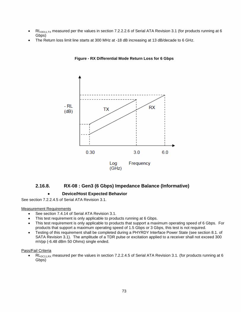
73
• RLDD11,TX measured per the values in section 7.2.2.2.6 of Serial ATA Revision 3.1 (for products running at 6 Gbps)
• The Return loss limit line starts at 300 MHz at -18 dB increasing at 13 dB/decade to 6 GHz.
Figure - RX Differential Mode Return Loss for 6 Gbps
2.16.8. RX-08 : Gen3 (6 Gbps) Impedance Balance (Informative) • Device/Host Expected Behavior
See section 7.2.2.4.5 of Serial ATA Revision 3.1. Measurement Requirements
• See section 7.4.14 of Serial ATA Revision 3.1. • This test requirement is only applicable to products running at 6 Gbps. • This test requirement is only applicable to products that support a maximum operating speed of 6 Gbps. For
products that support a maximum operating speed of 1.5 Gbps or 3 Gbps, this test is not required. • Testing of this requirement shall be completed during a PHYRDY Interface Power State (see section 8.1. of
SATA Revision 3.1). The amplitude of a TDR pulse or excitation applied to a receiver shall not exceed 300 mVpp (-6.48 dBm 50 Ohms) single ended.
Pass/Fail Criteria
• RLDC11,RX measured per the values in section 7.2.2.4.5 of Serial ATA Revision 3.1. (for products running at 6 Gbps)
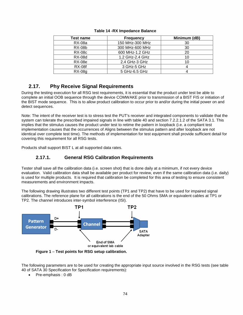
74
Table 14 -RX Impedance Balance
Test name Frequency Minimum (dB) RX-08a 150 MHz-300 MHz 30 RX-08b 300 MHz-600 MHz 30 RX-08c 600 MHz-1.2 GHz 20 RX-08d 1.2 GHz-2.4 GHz 10 RX-08e 2.4 GHz-3 GHz 10 RX-08f 3 GHz-5 GHz 4 RX-08g 5 GHz-6.5 GHz 4
2.17. Phy Receive Signal Requirements During the testing execution for all RSG test requirements, it is essential that the product under test be able to complete an initial OOB sequence through the device COMWAKE prior to transmission of a BIST FIS or initiation of the BIST mode sequence. This is to allow product calibration to occur prior to and/or during the initial power on and detect sequences. Note: The intent of the receiver test is to stress test the PUT's receiver and integrated components to validate that the system can tolerate the prescribed impaired signals in line with table 40 and section 7.2.2.1.2 of the SATA 3.1. This implies that the stimulus causes the product under test to retime the pattern in loopback (i.e. a compliant test implementation causes that the occurrences of Aligns between the stimulus pattern and after loopback are not identical over complete test time). The methods of implementation for test equipment shall provide sufficient detail for covering this requirement for all RSG tests. Products shall support BIST L at all supported data rates.
2.17.1. General RSG Calibration Requirements Tester shall save all the calibration data (i.e. screen shot) that is done daily at a minimum, if not every device evaluation. Valid calibration data shall be available per product for review, even if the same calibration data (i.e. daily) is used for multiple products. It is required that calibration be completed for this area of testing to ensure consistent measurements and environment impacts. The following drawing illustrates two different test points (TP1 and TP2) that have to be used for impaired signal calibrations. The reference plane for all calibrations is the end of the 50 Ohms SMA or equivalent cables at TP1 or TP2. The channel introduces inter-symbol interference (ISI).
Figure 1 – Test points for RSG setup calibration.
The following parameters are to be used for creating the appropriate input source involved in the RSG tests (see table 40 of SATA 30 Specification for Specification requirements):
• Pre-emphasis : 0 dB
75
• No CDR (Clock Data Recover unit) to be used for the jitter calibration. Real time scopes use a dataset derived clock, and BERTs use a 1.5, 3 or 6 GHz square wave direct from the jitter source dependent on data rate. More details available in MOIs.
The following table summarizes various calibrations that shall be referenced in later sections. In addition the table defines an order in which the calibrations have to be performed )i.e. step 1 through 4). Note: the UTD covers a range of products and therefore the table lists a superset of calibrations. When testing a product only the calibrations are required which apply for that particular product.
Table 15 – RSG Setup Calibration Steps and Settings
Step Test Point
Calibration Pattern
Method Gen1i Gen1m Gen2i Gen2m Gen3
1 Rise/ Fall Time
TP1 LFTP Section 7.4.4 in SATA 3.1 Specification
100 ps (20/80%) 100 ps (20/80%) 62 ps to 75 ps (20/80%)
2 Rj TP1 MFTP Section 7.4.12 of SATA 3.1 Specification, Rj method also applied to Gen1i/m and Gen2i/m
8.57 ps RMS (1 sigma for a 7 sigma 0.18 UI projection)
4.285 ps RMS (1 sigma for a 7 sigma 0.18 UI projection)
2.14 ps RMS (1 sigma for a 7 sigma 0.18 UI projection)
3 Sj TP1 MFTP Using Rj method defined in section 7.4.12 of SATA 3.1 Specification for all data rates
Sj=270 mUI Sj=270 mUI Sj=192 mUI
4 Tj TP2 FCOMP with 2 Aligns and new LBP section
See UTD section 2.17.1..1
Tj(min)=501 mUI Tj(max)=519 mUI Using a channel that introduces 40 ps ± 6 ps (i.e. min 34 ps and max 46 ps) of ISI in the given setup
Tj(min)=552 mUI Tj(max)=588 mUI Using a channel that introduces 40 ps ± 6 ps (i.e. min 34 ps and max 46 ps) of ISI in the given setup
Tj(min)=498 mUI Tj(max)=570 mUI Using a CIC that introduces a min 21 ps and max 33 ps of ISI in the given setup and that follows the definition in section 7.2.7 of SATA 3.1 Specification
5 Amplitude TP2 FCOMP with 2
For this test the amplitude
325 mV
240 mV
275 mV 240 mV
240 mV (Host), 200
76
Step Test Point
Calibration Pattern
Method Gen1i Gen1m Gen2i Gen2m Gen3
Aligns and new LBP section
distribution shall be either measured over a minimum 5E6 number of unit intervals at the 50% location of the bit interval using previously calibrated edge rates and jitter. It is required to ensure that the maximum allowed voltage is not exceeded. Sections 7.4.3 and 7.4.12 of SATA 3.1
Maximum not to exceed peak to peak voltage 600 mV
Maximum not to exceed peak to peak voltage 750 mV
mV (Device) Maximum not to exceed peak to peak voltage 1 V
2.17.1..1. Tj Measurement Method Rise/fall times, Rj and Sj are calibrated previously. Ensure that the channel in the calibration setup generates the specified amount of ISI. For Gen3i additionally the CIC requirements apply as defined in section 7.2.7 of SATA 3.1 Specification. Informative statement on ISI measurements at TP2: For ISI measurements turn off all other jitter. Rise/fall times are calibrated previously. Dry run results show that DDJ readings from oscilloscopes correlate well with a calculated delta of a TJ measurement with MFTP and a TJ measurement with LBP on a BERT. For each frequency f ∈ {5 MHz, 10 MHz, 33 MHz, 62 MHz} ensure that the Tj measured at TP2 is within the required range. The methodology of obtaining the appropriate configuration shall follow section 7.4.12 for Gen1i/m and Gen2i/m and section 7.4.13 for Gen3i of SATA 3.1 Specification. The Tj measurement shall be a clock to data measurement using a clean (i.e. jitter free) clock signal from the pattern generator.
2.17.2. RSG-01 : Gen1 (1.5 Gbps) Receiver Jitter Tolerance Test • Device/Host Expected Behavior
See sections 7.2.2.5.7 and 7.3 of Serial ATA Revision 3.1. Measurement Requirements
• See section 7.4.10 of SATA 3.1. See parameter details and calibration procedure for Gen1i/m in Section 2.17.1 of the UTD 1.4. The source amplitude shall be calibrated for Gen1i or Gen1m. This test requirement is applicable to all products. The data rate is 1.5 Gbps.
• The methods of implementation for test equipment shall provide sufficient detail for implementing the above high level procedure using specific test equipment.
Pass/Fail Criteria
• Test is run using the framed COMP pattern which contains 2 Aligns and the new LBP section for 10 minutes and verified to exhibit no more than zero frame errors for all four Sj frequencies:
o 10 MHz – RSG-01a
77
o 33 MHz – RSG-01b o 62 MHz – RSG-01c o 5 MHz – RSG-01d
• In the case where at least 1000 errors are observed during test execution, the test iteration may stop (i.e. test time < 10 minutes for a specific frequency due to high number of errors).
2.17.3. RSG-02 : Gen2 (3 Gbps) Receiver Jitter Tolerance Test • Device/Host Expected Behavior
See sections 7.2.2.5.7 and 7.3 of Serial ATA Revision 3.1. Measurement Requirements
• See section 7.4.10 of SATA 3.1. See parameter detail and calibration procedure for Gen2i/m in Section 2.17.1 of the UTD 1.4. The source amplitude shall be calibrated for Gen2i or Gen2m.
• This test requirement is only applicable to products claiming ability to run at 3 Gbps or 6 Gbps. The data rate is 3 Gbps.
• The methods of implementation for test equipment shall provide sufficient detail for implementing the above high level procedure using specific test equipment.
Pass/Fail Criteria
• Test is run using the FCOMP pattern with 2 Aligns and new LBP section for 5 minutes and verified to exhibit no more than zero frame errors all four Sj frequencies: o 10 MHz – RSG-02a o 33 MHz – RSG-02b o 62 MHz – RSG-02c o 5 MHz – RSG-02d
• In the case where at least 1000 errors are observed during test execution, the test iteration may stop (i.e. test time < 5 minutes for a specific frequency due to high number of errors).
2.17.4. RSG-03 : Gen3 (6 Gbps) Receiver Jitter Tolerance Test • Device/Host Expected Behavior
See sections 7.2.2.5.8 and 7.3 of SATA 3.1. Measurement Requirements
• See section 7.4.13 of SATA 3.1. See parameter detail and calibration procedure for Gen3 in Section 2.17.1 of the UTD 1.4.
• This test requirement is only applicable to products claiming the ability to run at 6 Gbps. The data rate is 6 Gbps.
• The methods of implementation for test equipment shall provide sufficient detail for implementing the above high level procedure using specific test equipment.
Pass/Fail Criteria
• Test is run using the FCOMP pattern with 2 Aligns and new LBP section for 2 minutes and 30 seconds and verified to exhibit no more than zero frame errors all four Sj frequencies: o 10 MHz – RSG-03a o 33 MHz – RSG-03b o 62 MHz – RSG-03c o 5 MHz – RSG-03d
• In the case where at least 1000 errors are observed during test execution, the test iteration may stop (i.e. test time < 2 minutes and 30 seconds for a specific frequency due to high number of errors).
78
2.17.5. RSG-04 : Reserved place holder
2.17.6. RSG-05 : Receiver Stress Test at +350 ppm • Device/Host Expected Behavior
See sections 7.2.2.5.7, and 7.3 of SATA 3.1. Measurement Requirements
• See section 7.4.12 of SATA 3.1. See parameter detail and calibration procedure for Gen1i/m in Section 2.17.1 of the UTD 1.4. The test is performed with all impaired signal conditions defined for Gen1i/m including Rj, Sj, ISI and Sj frequency is 62 MHz. The source amplitude shall be calibrated for Gen1i or Gen1m.
• This test requirement is applicable to all products. The data rate of the pattern generator is 1.5 Gbps + 350 ppm.
• The methods of implementation for test equipment shall provide sufficient detail for implementing the above high level procedure using specific test equipment.
Pass/Fail Criteria
• Test is run using the framed COMP pattern with 2 Aligns and new LBP section over a minimum of 18 successive iterations of the framed COMP pattern with 2 Aligns and new LBP section and verified to exhibit no more than zero frame errors. The pattern generator shall run asynchronously to the product under test.
• Note: If the test is conducted over more than 18 successive iterations of the framed COMP pattern with an observed frame error rate no greater than 8.2 X 10⁻⁸ (reference section 7.4.2.2 of the base SATA 3.1), the test is passed.
2.17.7. RSG-06 : Receiver Stress Test With SSC (Informative) • Device/Host Expected Behavior
See sections 7.2.2.1.5, 7.2.2.1.6, 7.2.2.5.7, and 7.3 of SATA 3.1. Intent of Test: Running with SSC at Gen1 rates is considered suitably stressful and eliminates the duplicity of tests at higher data rates. Measurement Requirements
• See section 7.4.12 of SATA 3.1. See parameter detail and calibration procedure for Gen1i/m in Section 2.17.1 of the UTD 1.4. The test is performed with all impaired signal conditions defined for Gen1i/m including Rj, Sj, ISI and Sj frequency is 62 MHz. The source amplitude shall be calibrated for Gen1i or Gen1m.
• This test requirement is applicable to all products. The data rate of the pattern generator is 1.5 Gbps - 350 ppm with an ideal 5000 ppm triangular downspread spread spectrum clock (SSC) at 33 kHz modulation frequency. I.e. the data rate range is between 1.5 Gbps - 5350 ppm and 1.5 Gbps - 350 ppm.
• The methods of implementation for test equipment shall provide sufficient detail for implementing the above high level procedure using specific test equipment.
Pass/Fail Criteria
• Test is run using the framed COMP pattern with 2 Aligns and new LBP section over a minimum of 18 successive iterations of the framed COMP pattern with 2 Aligns and new LBP section and verified to exhibit no more than zero frame errors. The pattern generator must run asynchronously to the product under test.
• Note: If the test is conducted over more than 18 successive iterations of the framed COMP pattern with an observed frame error rate no greater than 8.2 X 10⁻⁸ (reference section 7.4.1.2 of the base SATA 3.1), the test is passed.
2.18. Phy OOB Requirements Min and max pulse and gap widths shall consider both the +100 mV and the -100 mV edges for determining starting and ending times.
79
2.18.1. OOB-01 : OOB Signal Detection Threshold • Device/Host Expected Behavior
See section 7.2.2.6.2 of Serial ATA Revision 3.1. Measurement Requirements
• See section 7.4.25 of Serial ATA Revision 3.1. • Note that the Specification stipulates a Detection Threshold with value of Vthresh, where Vthresh is 50 ≤ Vthresh ≤
200 mV for 1.5 Gbps products, and where Vthresh is 75 ≤ Vthresh ≤ 200 mV for 3 Gbps and 6 Gbps products. For the interests of the Interoperability Program, the measurements shall only be taken to verify this requirement at the lower and upper limits. The signal amplitude level of the source generator shall be validated using a mode voltage measurement at 0.45 to 0.55 UI.
• To execute this test on a device which supports a maximum data rate of 1.5 Gbps (i.e. Gen 1 only), a COMINIT/COMRESET burst is issued to the product at the following voltage threshold limits: o OOB-01a - 40 mV (at this limit, the product is expected to NOT detect the OOB signaling) o OOB-01b - 210 mV (at this limit, the product is expected to detect the OOB signaling)
• To execute this test on a device which supports a maximum data rate of 3 Gbps or 6 Gbps, a COMINIT/COMRESET burst is issued to the product at the following voltage threshold limits: o OOB-01c - 60 mV (at this limit, the product is expected to NOT detect the OOB signaling) o NOTE : Tool resolution preference is even values, as opposed to 75 mV o OOB-01d - 210 mV (at this limit, the product is expected to detect the OOB signaling)
• NOTE: In a case where a device supports Asynchronous Signal Recovery, it is possible that a device may transmit COMINIT pro-actively and not in direct response to a COMRESET. In verification of this test requirement, it is essential that the tester be able to extract any COMINIT response which may be as a result of Asynchronous Signal Recovery, and simply verify COMINIT responses as a result of COMRESET receipt from the host.
• Suggested test methodology requires sending the following test sequence continuously from a suitable generator: 6 x (COMINIT/COMRESET burst + 480 UIOOB gap) + 1 x (45,000 UIOOB gap)
1) Using a suitable instrument (e.g. real-time scope or equivalent) to observe a minimum continuous 2 ms
window, verify that the PUT consistently responds to each COMINIT/COMRESET burst. 2) Detection Tests: Changing the COMINIT/COMRESET burst amplitude values only, verify that the PUT
continues to consistently respond to a COMINIT/COMRESET Burst amplitude value of 210 mV. 3) No-Detection Tests: Changing the COMINIT/COMRESET burst amplitude values only, verify that the PUT
consistently DOES NOT respond to an COMINIT/COMRESET burst amplitude value of 40 mV for 1.5 Gbps products (60 mV for 3 Gbps and 6 Gbps products), with the exception of unsolicited COMINIT bursts due to ASR (see note above).
Pass/Fail Criteria
• For products with a maximum data rate of 1.5 Gbps: o OOB-01a - Verification of no product COMINIT/COMRESET detection at 40 mV o OOB-01b - Verification of product COMINIT/COMRESET detection at 210 mV o If any of the above cases fails, this is considered a failure by the product.
• For products with a maximum data rate of 3 Gbps or 6 Gbps: o OOB-01c - Verification of no product COMINIT/COMRESET detection at 60 mV o OOB-01d - Verification of product COMINIT/COMRESET detection at 210 mV o If any of the above cases fails, this is considered a failure by the product.
2.18.2. OOB-02 : UI During OOB Signaling • Device/Host Expected Behavior
See section 7.2.2.6.3 of Serial ATA Revision 3.1.
80
Pass/Fail Criteria
• Mean UIOOB measured to be between 646.67 ps and 686.67 ps over entire OOB burst
2.18.3. OOB-03 : COMINIT/RESET and COMWAKE Transmit Burst Length • Device/Host Expected Behavior
See section 7.2.2.6.4 of Serial ATA Revision 3.1. Measurement Requirements
• See section 7.4.26 of Serial ATA Revision 3.1. • This test is only run once at the maximum interface rate of the product (1.5 Gbps 3 Gbps or 6 Gbps). • Note that the requirement within the Specification is called out in UI. For the interests of the Interoperability
Program, the measured value (T) shall be compared against the minimum and maximum values of a multiple of UIOOB in nanoseconds, where 103.5 ≤ T ≤ 110.9 (+1% Larger than Spec Limit). The values above are obtained from the following formulas: o Min (160) = 646.67 ps (Min UIoob) x 160 = 103.5ns o Max (160) = 686.67 ps (+1%) (Max UIoob) x 160 = 110.9 ns (Note: +1% on OOB is what gets measured,
which requires a 4% margin rather than the current spec’d 3% margin.)
A minimum of 5 COMINIT/RESET and 5 COMWAKE bursts shall be captured and the mean of all captured values shall be reported. Pass/Fail Criteria
• Burst Length measured to be between minimum and maximum values of UIOOB multiplied by 160 (in nanoseconds)
2.18.4. OOB-04 : COMINIT/RESET Transmit Gap Length • Device/Host Expected Behavior
See section 7.2.2.6.5 of Serial ATA Revision 3.1. Measurement Requirements
• See section 7.4.26 of Serial ATA Revision 3.1. • This test is only run once at the maximum interface rate of the product (1.5 Gbps, 3 Gbps or 6 Gbps). • Note that the requirement within the Specification is called out in UI. For the interests of the Interoperability
Program, the measured value (T) shall be compared against the minimum and maximum values of a multiple of UIOOB in nanoseconds, where 310.4 ≤ T ≤ 329.6. The values above are obtained from the following formulas: o Min (480) = 646.67 ps (Min UIoob) x 480 = 310.4 ns o Max (480) = 686.67 ps (Max UIoob) x 480 = 329.6 ns
• Per definition, devices shall be validated against the COMINIT Transmit Gap Length and hosts shall be verified against the COMRESET Transmit Gap Length. The requirement is the same in both cases.
Pass/Fail Criteria
• Gap Length measured to be between minimum and maximum values of UIOOB multiplied by 480 (in nanoseconds)
2.18.5. OOB-05 : COMWAKE Transmit Gap Length • Device/Host Expected Behavior
See section 7.2.2.6.6 of Serial ATA Revision 3.1. Measurement Requirements
81
• See section 7.4.26 of Serial ATA Revision 3.1. • This test is only run once at the maximum interface rate of the product (1.5 Gbps, 3 Gbps or 6 Gbps). • Note that the requirement within the Specification is called out in UI. For the interests of the Interoperability
Program, the measured value (T) shall be compared against the minimum and maximum values of a multiple of UIOOB in nanoseconds, where 102.4 (-1% smaller than Spec Limit) ≤ T ≤ 109.9. The values above are obtained from the following formulas:
o Min (160) = 646.67 ps (-1%) (Min UIoob) x 160 = 102.4 ns o Max (160) = 686.67 ps (Max UIoob) x 160 = 109.9 ns
Pass/Fail Criteria
• Gap Length measured to be between minimum and maximum values of UIOOB multiplied by 160 (in nanoseconds)
2.18.6. OOB-06 : COMWAKE Gap Detection Windows • Device/Host Expected Behavior
See section 7.2.2.6.7 of Serial ATA Revision 3.1. Measurement Requirements • See section 7.4.26 of Serial ATA Revision 3.1. • This test is only run once at the maximum interface rate of the product (1.5 Gbps, 3 Gbps or 6 Gbps). • Note that the Specification stipulates a Detection Window with value of T, where T is 35 ≤ T < 175 in
nanoseconds. For the interests of the Interoperability Program, the measurements shall only be taken to verify this requirement at the lower and upper limits.
• To execute this test, a COMWAKE is issued to the product at the following limits: o 153 UIOOB (at this limit, the product is expected to respond with COMWAKE) o 167 UIOOB (at this limit, the product is expected to respond with COMWAKE) o 45 UIOOB (at this limit, the product is expected to NOT respond with COMWAKE) o 266 UIOOB (at this limit, the product is expected to NOT respond with COMWAKE)
• NOTE : There is no timing requirement for how soon following a host COMWAKE which the device shall respond with a device COMWAKE, and vice versa. For test efficiency purposes, a tester is only required to wait for verification of device COMWAKE up to 100ms following de-qualification of host COMWAKE, and vice versa.
• Suggested test methodology requires sending the following test sequence continuously from a suitable generator:
For Devices: 6 x (COMINIT/COMRESET burst + 480 UIOOB gap) + 1 x (45,000 UIOOB gap) + 6 x (COMWAKE burst + 160 UIOOB gap) + 1 x (130,000 UIOOB gap) For Hosts: 6 x (COMINIT burst + 480 UIOOB gap) + 1 x (300,000 UIOOB gap) + 6 x (COMWAKE burst + 160 UIOOB gap) + 1 x (130,000 UIOOB gap)
1) Using a suitable instrument (e.g. real-time scope or equivalent) to observe a minimum continuous 2ms
window, verify that the PUT consistently responds to each OOB sequence by entering speed negotiation accordingly. Figure 2 below shows an example screen capture of typical PUT behavior for nominal COMINIT/COMRESET and COMWAKE gaps:
82
Figure - 2 Example OOB-06 test stimulus and PUT response, nominal COMINIT/COMRESET, COMWAKE (Test stimulus top, yellow. PUT response bottom, purple.)
2) Detection Tests: Changing the COMWAKE gap values only, verify that the PUT continues to consistently
enter speed negotiation for gap values of 155 and 165 UIOOB (103.33 and 110 ns, respectively)
3) No-Detection Tests: Changing the COMWAKE gap values only, verify that the PUT consistently DOES NOT enter speed negotiation for gap values of 45 and 266 UIOOB (30 and 177.33 ns, respectively). An example screenshot of typical PUT behavior appears in Figure 3 below. (Note lack of speed negotiation sequence from PUT.)
Figure - 3 Example OOB-06 test stimulus and PUT response for out-of-range COMWAKE (Test stimulus top, yellow. PUT response bottom, purple.)
A minimum of 5 COMINIT/RESET and 5 COMWAKE bursts shall be captured and the mean of all captured values shall be reported.
83
Pass/Fail Criteria
• OOB-06a - Verification of product COMWAKE response at 155 UIOOB • OOB-06b - Verification of product COMWAKE response at 165 UIOOB • OOB-06c - Verification of no product COMWAKE response at 45 UIOOB • OOB-06d - Verification of no product COMWAKE response at 266 UIOOB • If any of the above cases fails, this is considered a failure by the product.
2.18.7. OOB-07 : COMINIT/COMRESET Gap Detection Windows • Device/Host Expected Behavior
See section 7.2.2.6.8 of Serial ATA Revision 3.1. Measurement Requirements
• See section 7.4.26 of Serial ATA Revision 3.1. • This test is only run once at the maximum interface rate of the product (1.5 Gbps, 3 Gbps or 6 Gbps). • Note that the Specification stipulates a Detection Window with value of T, where T is 175 ≤ T < 525 in
nanoseconds. For the interests of the Interoperability Program, the measurements shall only be taken to verify this requirement at the lower and upper limits.
To execute this test on a device, a COMRESET is issued to the device at the following limits:
459UIOOB (at this limit, the device is expected to respond with COMINIT) 501UIOOB (at this limit, the device is expected to respond with COMINIT) 259UIOOB (at this limit, the device is expected to NOT respond with COMINIT) 791UIOOB (at this limit, the device is expected to NOT respond with COMINIT)
NOTE : A device is required to respond by transmitting COMINIT within 10ms of de-qualification of a received COMRESET signal (see section 8.4.1 of Serial ATA Revision 3.1). With this in mind, a test only needs to wait up to 11 ms following de-qualification of COMRESET to ensure that the device is responding. If no COMINIT is received in this timeframe, this is considered a failure by the device to this test. NOTE : In a case where a device supports Asynchronous Signal Recovery, it is possible that a device may transmit COMINIT pro-actively and not in direct response to a COMRESET. In verification of this test requirement, it is essential that the tester be able to extract any COMINIT response which may be as a result of Asynchronous Signal Recovery, and simply verify COMINIT responses as a result of COMRESET receipt from the host. To execute this test on a host, a COMINIT is issued to the host at the following limits:
• 459 UIOOB (at this limit, the host is expected to respond with COMWAKE) • 501 UIOOB (at this limit, the host is expected to respond with COMWAKE) • 259 UIOOB (at this limit, the host is expected to NOT respond with COMWAKE) • 791 UIOOB (at this limit, the host is expected to NOT respond with COMWAKE)
Suggested test methodology requires sending the following test sequence continuously from a suitable generator: For Device: 6 x (COMINIT/COMRESET burst + 480 UIOOB gap) + 1 x (45,000 UIOOB gap) For Host: 6 x (COMINIT/COMRESET burst + 480 UIOOB gap) + 1 x (300,000 UIOOB gap)
84
1) Using a suitable instrument (e.g. real-time scope or equivalent) to observe a minimum continuous 2 ms window, verify that the PUT consistently responds to each COMINIT/COMRESET. Figure 4 below shows a typical screen capture of proper PUT behavior for nominal COMINIT/COMRESET gaps:
Figure - 4 Example OOB-07 test stimulus and PUT response, for nominal COMINIT/COMRESET gap (Test stimulus top, yellow. PUT response bottom, purple.)
2) Detection Tests: Changing the COMINIT/COMRESET gap values only, verify that the PUT continues to
respond to gap values of 459 and 501 UIOOB (306 and 334 ns, respectively)
3) No-Detection Tests: Changing the COMINIT/COMRESET gap values only, verify that the PUT consistently DOES NOT respond to gap values of 259 and 791 UIOOB (172.66 and 527.3 3ns, respectively), with the exception of unsolicited COMINIT bursts due to ASR (see note above). An example screenshot of typical PUT behavior appears in Figure 5 below.
Figure - 5 Example OOB-07 test stimulus and PUT response for out-of-range COMINIT/COMRESET (Test stimulus top, yellow. PUT response bottom, purple.)
A minimum of 5 COMINIT/RESET and 5 COMWAKE bursts shall be captured and the mean of all captured values shall be reported. Pass/Fail Criteria
85
• Device: o OOB-07a - Verification of COMINIT response at 459 UIOOB o OOB-07b - Verification of COMINIT response at 501 UIOOB o OOB-07c - Verification of no COMINIT response at 259 UIOOB o OOB-07d - Verification of no COMINIT response at 791 UIOOB
• Host: o OOB-07a - Verification of COMWAKE response at 459 UIOOB o OOB-07b - Verification of COMWAKE response at 501 UIOOB o OOB-07c - Verification of no COMWAKE response at 259 UIOOB o OOB-07d - Verification of no COMWAKE response at 791 UIOOB
• If any of the above cases fails, this is considered a failure by the product.
2.19. Port Multiplier Requirements (informative) Devices used for testing Port Multipliers shall be limited to HDD type devices. All tests in this section are intended to be run in a configuration based on a Port Multiplier Aware Host. A Port Multiplier Aware Host is defined by the two following characteristics:
1. A hardware platform in which at least one HBA (resident in the motherboard chipset or on a separate PCB) is capable of using non-zero values in the PM Port field in the FISes it sends and receives.
2. An OS and OS device driver which shall discover and enumerate any attached port multipliers during system initialization.
2.19.1. PM-01 : Device Port 0 Enabled by Default • Expected Behavior:
See sections 16.2 and 16.3.3.3 of Serial ATA Revision 3.1. Serial ATA Revision 3.1 requires that a host system that has no explicit support for Port Multipliers shall work with a device connected to PM device port 0. In this configuration the PM is transparent to both host and device, with the exception of time required for a transmission from one end device to the other. More specifically, a host system should be able to issue Soft Reset and all the commands used during a boot sequence to a device attached to PM port 0, with results identical to those obtained when the same device is directly attached to a SATA HBA. For UTD 1.4 we shall execute a series of representative commands. We shall not actually boot a system in this test. Port Multiplier testing shall require a modification to the UTD 1.2 System Interop test. Booting a non-PM aware system from a Port Multiplier port 0 device shall be a part of the modified test. Measurement Requirements
• Attach a SATA HDD to port 0 of the PM. Apply power to the PM, the drive, and the host system. • To emulate host system that has no explicit support for Port Multipliers, issue Soft Reset to Port 0 of the port
multiplier before starting the test sequence. • Execute the following ATA commands as defined in ATA-8_ACS_r4b:
1. IDENTIFY DEVICE 2. SET FEATURES with Features Register = 02h (Enable Write Cache) or a similarly benign Feature
Register value. 3. WRITE DMA with one sector of nonzero data to LBA 0. 4. READ DMA from LBA 0.
Pass/Fail Criteria
• A correct HDD Signature FIS (34h) is received following power on, before the soft reset is issued. • A correct HDD Signature FIS (34h) is received in response to the soft reset.
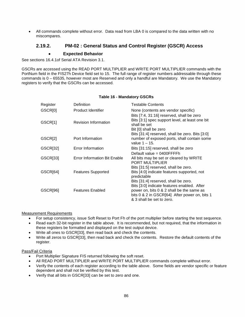
86
• All commands complete without error. Data read from LBA 0 is compared to the data written with no miscompares.
2.19.2. PM-02 : General Status and Control Register (GSCR) Access • Expected Behavior
See sections 16.4.1of Serial ATA Revision 3.1. GSCRs are accessed using the READ PORT MULTIPLIER and WRITE PORT MULTIPLIER commands with the PortNum field in the FIS27h Device field set to 15. The full range of register numbers addressable through these commands is 0 – 65535, however most are Reserved and only a handful are Mandatory. We use the Mandatory registers to verify that the GSCRs can be accessed.
Table 16 - Mandatory GSCRs
Register Definition Testable Contents GSCR[0] Product Identifier None (contents are vendor specific)
GSCR[1] Revision Information Bits [7:4, 31:16] reserved, shall be zero Bits [3:1] spec support level, at least one bit shall be set Bit [0] shall be zero
GSCR[2] Port Information Bits [31:4] reserved, shall be zero. Bits [3:0] number of exposed ports, shall contain some value 1 – 15.
GSCR[32] Error Information Bits [31:15] reserved, shall be zero
GSCR[33] Error Information Bit Enable Default value = 0400FFFFh All bits may be set or cleared by WRITE PORT MULTIPLIER
GSCR[64] Features Supported Bits [31:5] reserved, shall be zero. Bits [4:0] indicate features supported, not predictable
GSCR[96] Features Enabled
Bits [31:4] reserved, shall be zero. Bits [3:0] indicate features enabled. After power on, bits 0 & 2 shall be the same as bits 0 & 2 in GSCR[64] After power on, bits 1 & 3 shall be set to zero.
Measurement Requirements
• For setup consistency, issue Soft Reset to Port Fh of the port multiplier before starting the test sequence. • Read each 32-bit register in the table above. It is recommended, but not required, that the information in
these registers be formatted and displayed on the test output device. • Write all ones to GSCR[33], then read back and check the contents. • Write all zeros to GSCR[33], then read back and check the contents. Restore the default contents of the
register. Pass/Fail Criteria
• Port Multiplier Signature FIS returned following the soft reset. • All READ PORT MULTIPLIER and WRITE PORT MULTIPLIER commands complete without error. • Verify the contents of each register according to the table above. Some fields are vendor specific or feature
dependent and shall not be verified by this test. • Verify that all bits in GSCR[33] can be set to zero and one.
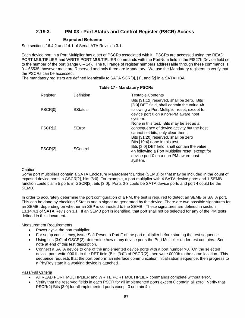
87
2.19.3. PM-03 : Port Status and Control Register (PSCR) Access • Expected Behavior
See sections 16.4.2 and 14.1 of Serial ATA Revision 3.1. Each device port in a Port Multiplier has a set of PSCRs associated with it. PSCRs are accessed using the READ PORT MULTIPLIER and WRITE PORT MULTIPLIER commands with the PortNum field in the FIS27h Device field set to the number of the port (range 0 – 14). The full range of register numbers addressable through these commands is 0 – 65535, however most are Reserved and only three are Mandatory. We use the Mandatory registers to verify that the PSCRs can be accessed. The mandatory registers are defined identically to SATA SCR[0], [1], and [2] in a SATA HBA.
Table 17 - Mandatory PSCRs
Register Definition Testable Contents
PSCR[0] SStatus
Bits [31:12] reserved, shall be zero. Bits [3:0] DET field, shall contain the value 4h following a Port Multiplier reset, except for device port 0 on a non-PM aware host system.
PSCR[1] SError None in this test. Bits may be set as a consequence of device activity but the host cannot set bits, only clear them.
PSCR[2] SControl
Bits [31:20] reserved, shall be zero Bits [19:4] none in this test. Bits [3:0] DET field, shall contain the value 4h following a Port Multiplier reset, except for device port 0 on a non-PM aware host system.
Caution: Some port multipliers contain a SATA Enclosure Management Bridge (SEMB) or that may be included in the count of exposed device ports in GSCR[2], bits [3:0]. For example, a port multiplier with 4 SATA device ports and 1 SEMB function could claim 5 ports in GSCR[2], bits [3:0]. Ports 0-3 could be SATA device ports and port 4 could be the SEMB. In order to accurately determine the port configuration of a PM, the test is required to detect an SEMB or SATA port. This can be done by checking SStatus and a signature generated by the device. There are two possible signatures for an SEMB, depending on whether an SEP is connected to the SEMB. These signatures are defined in section 13.14.4.1 of SATA Revision 3.1. If an SEMB port is identified, that port shall not be selected for any of the PM tests defined in this document. Measurement Requirements
• Power cycle the port multiplier. • For setup consistency, issue Soft Reset to Port F of the port multiplier before starting the test sequence. • Using bits [3:0] of GSCR(2), determine how many device ports the Port Multiplier under test contains. See
note at end of this test description. • Connect a SATA device to one of the implemented device ports with a port number >0. On the selected
device port, write 0001b to the DET field (Bits [3:0]) of PSCR(2), then write 0000b to the same location. This sequence requests that the port perform an interface communication initialization sequence, then progress to a PhyRdy state if a working device is attached.
Pass/Fail Criteria
• All READ PORT MULTIPLIER and WRITE PORT MULTIPLIER commands complete without error. • Verify that the reserved fields in each PSCR for all implemented ports except 0 contain all zero. Verify that
PSCR(2) Bits [3:0] for all implemented ports except 0 contain 4h.
88
• On the port with the attached SATA device, check the DET field in PSCR(0) and confirm that it contains 3h. This confirms that communication has been established, and indirectly confirms that the two WRITE PORT MULTIPLIER were correctly executed. (Note: it may be necessary to reset the X bit in PSCR1 before a READ PORT MULTIPLIER to PSCR0 is expected to succeed.)
2.19.4. PM-04 : 3 Gbps Backwards Compatibility • Expected Behavior
See section 7.4.26.1.2 of Serial ATA Revision 3.1. If a device claims support for Serial ATA Gen-2 signaling speed, 3 Gbps, (Word 76 bit 2 set to one in IDENTIFY DEVICE or IDENTIFY PACKET DEVICE data), then it shall also support Serial ATA Gen-1 signaling speed, 1.5 Gbps, (Word 76 bit 1 set to one in IDENTIFY DEVICE or IDENTIFY PACKET DEVICE data). 1. If the HBA supports only 1.5 Gbps signaling then a 3 Gbps capable port multiplier shall negotiate for 1.5 Gbps operation on the host port. A compliant HBA can be forced to operate at Gen1-only speed through the SPD field of the SControl register in the HBA. 2. If a device supports only 1.5 Gbps signaling then a 3 Gbps capable port multiplier shall negotiate for 1.5 Gbps operation on the device port. There is not a standard way to force a Gen2 device to operate at Gen1-only speed. For this test it shall be necessary to either use a Gen1-only device or use a vendor unique method for restricting a Gen2 device to Gen1 speed. Measurement Requirements
• For setup consistency, issue Soft Reset to Port F of the port multiplier before starting the test sequence. • Determine the native speed of the PM host interface by enabling the attached HBA port for Gen2 speed and
observing the negotiated speed after a COMRESET sequence. If the PM is limited to Gen1 speed, then skip this test, as 3 Gbps backward compatibility does not apply.
1. Attach a port multiplier to a host SATA port that is restricted to 1.5 Gbps. Force a COMRESET sequence on
the host SATA port. 2. Attach a Gen1-only device to a port multiplier device port enabled for 3 Gbps operation. Force a
COMRESET sequence on the device port.
Pass/Fail Criteria • Observe in the HBA SStatus register that the interface is Active and the negotiated speed is 1.5 Gbps. • Observe in the PSCR SStatus register for the device port under test that the interface is Active and the
negotiated speed is 1.5 Gbps.
2.19.5. PM-05 : Interface Power Management, H – PM, Host Initiated • Expected Behavior
See sections 14.1 and 16.3.3.6 of Serial ATA Revision 3.1. A port multiplier is required to respond to PMREQ_P and PMREQ_S on its host port with either PMACK or PMNAK. Actual support of the low power link states is optional. If a port multiplier responds to PMREQ_P and PMREQ_S on its host port with PMACK , then it required to propagate the request to all active device ports. Measurement Requirements
• For setup consistency, issue Soft Reset to Port F of the port multiplier before starting the test sequence.
a) Determine whether low power modes are supported by the port multiplier.
89
Issue COMRESET from the HBA port to the host port of the PM and allow time for the sequence to complete. Verify that the H-PM interface is in active state. Issue PMREQ_P to the device using the SPM field of the HBA SPM register or through a vendor specific method. Ensure that the H-PM interface goes to partial state. Issue COMWAKE and ensure that the H-PM interface goes to active state. If either of these conditions is not met, put out a message, “Host – PM interface failed HIPM partial test.” Issue PMREQ_S to the device using the SPM field of the HBA SPM register or through a vendor specific method. Ensure that the PM-Dev interface goes to slumber state. Issue COMWAKE and ensure that the PM-Dev interface goes to active state. If either of these conditions is not met, put out a message, “Host – PM interface failed HIPM slumber test. If the partial and slumber tests above are successful, proceed with testing. If they are not successful, issue the message, “Link low power states not supported by port multiplier” and end test PM-05. A host emulator/analyzer can also be used for these tests. Procedures are not documented here.
b) PM propagates PMREQ to all active device ports. Attach an HDD supporting HIPM to a device port. Issue COMRESET to the PM host port and allow time for the sequence to complete. Initialize the interface to the attached HDD. Verify that the device port interface is active. Issue PMREQ_P to the PM host port. Read the IPM field in the SStatus register in the selected device port and record the state of the device port interface. (Sending a FIS27h with the READ PORT MULTIPLIER command should generate a COMWAKE on the H-PM interface to allow communicating with the PM, without awakening the PM-Dev interface.) Repeat this step, starting with COMRESET, sending PMREQ_S instead of PMREQ_P.
c) PM partial state exit latency Connect a bus analyzer to the H-PM interface. Start the analyzer. An oscilloscope or logic analyzer can be used instead. Place the H-PM interface into partial state as described in step A. Issue the COMWAKE OOB signal as described in step B. Stop the bus analyzer or other device recording interface activity. Record the time between the end of the COMWAKE burst from the host to the end of the ALIGN burst following the COMWAKE burst from the PM.
d) PM slumber state exit latency Connect a bus analyzer to the H-PM interface. Start the analyzer. An oscilloscope or logic analyzer can be used instead. Place the H-PM interface into partial state as described in step A. Issue the COMWAKE OOB signal as described in step B.
90
Stop the bus analyzer or other device recording interface activity. Record the time between the end of the COMWAKE burst from the host to the end of the ALIGN burst following the COMWAKE burst from the PM.
• One execution of step a) is required for this test. • Ten iterations each of steps b) and c) above are required for this test.
Pass/Fail Criteria
a) Determine whether low power modes are supported by the port multiplier. Informative only, not subject to pass/fail evaluation. May cause the rest of PM-05 to be skipped.
b) PM propagates PMREQ to all active device ports. Verify that the PM-Dev interface is in partial state following the first pass through this step and in slumber state following the second pass through this step. If both states are as expected, the test result is PASS. If either state is incorrect, the test result is FAIL.
c) PM partial state exit latency. Verify that the times recorded for this step are all 10 us or less. If any time exceeds 10 us, then the result of this test step is FAIL.
d) PM slumber state exit latency. Verify that the times recorded for this step are all 10 ms or less. If any time exceeds 10 ms, then the result of this test step is FAIL.
2.19.6. PM-06 : Interface Power Management, H - PM, PM Initiated • Expected Behavior
See sections 14.1 and 16.3.3.6 of Serial ATA Revision 3.1. A port multiplier may optionally support issuing power management requests to the host (PIPM) when all device ports are in a low power state or disabled. This capability, if supported, may be enabled or disabled by writing to bit 1 of GSCR(96). There is no standard way to control which form of PMREQ is generated by a port multiplier. There are three scenarios that can result in a PIPM request.
a) The last Active device port on the PM transitions to Disabled state as a result of the host writing 0100b to the DET field of the SControl register for that port.
b) The last Active device port on the PM transitions to Slumber or Partial state as the result of a HIPM request directed to the device on that port.
c) A DIPM request from the device attached to the last Active device port on the PM. Measurement Requirements
• For setup consistency, issue Soft Reset to Port F of the port multiplier before starting the test sequence. • Attach and power up an HDD to a PM device port with a port number >0.
a) Verify that the port multiplier supports issuing PMREQ to the host.
Issue COMRESET from the HBA port to the host port of the PM and allow time for the sequence to complete. Check PM GSCR[64] bit 1. If bit 1 = 0, skip the rest of PM-06 and put out a message, “Port multiplier does not support issuing PMREQ to
91
the host.” If bit 1 = 1, set PM GSCR[96] bit 1 = 1.
b) Verify that the PM issues a PMREQ when one of the three scenarios described above occurs. All device ports shall have been disabled by the COMRESET. This meets the requirement of scenario a) above. Wait 10 seconds. Check the state of the H-PM interface by reading the IPM field of the HBA SStatus register. If the interface is in partial or slumber state, continue to step c. If the H-PM interface is still in active state, then initialize the interface to the attached HDD. Issue PMREQ_S to the attached HDD. This can be done by writing first 0010b, then 0000b, to the SPM field of the device port SControl field. Wait 10 seconds. Check the state of the H-PM interface by reading the IPM field of the HBA SStatus register. If the interface is in partial or slumber state, continue to step c. If the H-PM interface is still in active state, check that the drive supports DIPM (IDENTIFY DEVICE Word 78 Bit 3), enable the DIPM feature in the drive using the SET FEATURES command, then issue a STANDBY IMMEDIATE command to the attached HDD. Wait 10 seconds. Check the state of the H-PM interface by reading the IPM field of the HBA SStatus register. If the drive does not support DIPM or if none of these three scenarios has resulted in the H-PM interface entering partial or slumber state, put out a message for this subtest saying “Unable to generate a port multiplier initiated partial or slumber state on the host – PM interface.” This condition shall be recorded as na, not FAIL.
Pass/Fail Criteria Test b) Shall be repeated 10 times.
a) Verify that the port multiplier supports issuing PMREQ to the host. Informative only, not subject to pass/fail evaluation. May cause the rest of PM-06 to be skipped.
b) Verify that the PM issues a PMREQ when one of the three scenarios described above occurs. If the H-PM interface enters partial or slumber state at least once, then the test result is PASS. If the H-PM interface does not enter partial or slumber state at least once, then the test result is na.
2.19.7. PM-07 : Interface Power Management, PM - Dev, PM Initiated • Expected Behavior
See sections 16.3.3.6 of Serial ATA Revision 3.1. On this interface the port multiplier device port is seen as a host port by the attached device. The device shall respond to IPM requests and to COMWAKE as if it were directly attached to an HBA. Measurement Requirements
• For setup consistency, issue Soft Reset to Port F of the port multiplier before starting the test sequence.
a) Verify that the device supports HIPM. Attach an HDD to the selected device port. Initialize the PM-Dev interface. This can be done through the DET field of the SControl register of the device port.
92
Issue an IDENTIFY DEVICE command to the device and check IDENTIFY DEVICE word 76 bit 9. If bit 9 = 1, then the device supports host (PM) initiated interface power management. Continue with the test. If bit 9 = 0, then the device does not support HIPM. In that case, put out a message saying “The device does not support HIPM.” Skip the remainder of this test.
b) Verify correct PM-initiated IPM behavior on the selected device port. Initialize the PM-Dev interface. Ensure the interface is in the Active state. Issue PMREQ_P to the device using the SPM field of the device port SPM register. Ensure that the PM-Dev interface goes to partial state. Issue COMWAKE and ensure that the PM-Dev interface goes to active state. If any of these conditions is not met, put out a message, “PM-Dev interface failed HIPM partial test”. Initialize the PM-Dev interface. Ensure the interface is in the Active state. Issue PMREQ_S to the device using the SPM field of the device port SPM register. Verify that the PM-Dev interface goes to slumber state. Issue COMWAKE and ensure that the PM-Dev interface goes to active state. If any of these conditions is not met, put out a message, “PM-Dev interface failed HIPM slumber test”.
Pass/Fail Criteria Test b) Shall be repeated 10 times.
a) Verify that the device supports HIPM. Informative only, not subject to pass/fail evaluation. May cause the rest of PM-07 to be skipped.
b) Verify correct PM-initiated IPM behavior on the selected device port. If the interface state is correct at each verification point in all 10 iterations of this test, then the result is PASS. If the interface is in an incorrect state at any verification point during the 10 iterations of this test then the result is FAIL.
2.19.8. PM-08 : Interface Power Management, PM - Dev, Dev Initiated • Expected Behavior
See sections 16.3.3.6 of Serial ATA Revision 3.1. Device initiated interface power management requests shall affect the PM-Dev link on which they are issued but shall not affect the interface power state of other device ports or the H-PM interface. There is no standard method to force a device to issue an IPM request, although devices with DIPM enabled shall generally do so within 10 seconds after receiving a STANDBY IMMEDIATE command. Measurement Requirements For setup consistency, issue Soft Reset to Port F of the port multiplier before starting the test sequence.
a) Verify that the device supports DIPM Connect an HDD to a device port in the port multiplier. Initialize the PM-Dev interface for that port and verify that the interface is in active state. Check that the drive supports DIPM (IDENTIFY DEVICE Word 78 Bit 3 = 1), enable the DIPM feature in the drive using the SET FEATURES command, then issue a STANDBY IMMEDIATE command to the attached HDD. Wait 10 seconds.
93
Check the state of the PM-DEV interface by reading the IPM field of the PM device port SStatus register. If the interface is in partial or slumber state, proceed with this test. If the interface is still active after 10 repetitions of this step, then bypass the rest of this test and generate the message, “Unable to generate DIPM request. PM-08 skipped”.
b) DIPM requests do not affect other device ports or the PM host port. Leaving the HDD in step a) connected, connect a second HDD to a different device port. Do not enable DIPM on the second HDD. Initialize both device interfaces. Ensure that the host H-PM interface and both PM-Dev interfaces are active. Enable DIPM in the first HDD and issue a STANDBY IMMEDIATE command to the first drive. Wait 10 seconds. Record the states of the H-PM interface and both PM-Dev interfaces.
c) PM device port partial/slumber state exit latency There is no standard way to cause a device to issue COMWAKE. This test step is a placeholder until a mechanism is defined to allow testing.
Pass/Fail Criteria Test b) Shall be repeated 10 times.
a) Verify that the device supports DIPM Informative only, not subject to pass/fail evaluation. • For each iteration of the test, if the H-PM interface and the second PM-Dev interface are active, and the
first PM-Dev interface is in partial or standby state, then the result for this iteration is PASS. If either the H-PM interface or the second PM-Dev interface is in partial or slumber state, then the result for this iteration is FAIL. If all three interfaces are in active state, the result for this iteration is na. Repeat test step b) 10 times. If there is at least one PASS result and no FAIL results, then the test result is PASS. If there is one or more FAIL results, then the test result is FAIL. If all 10 results are na, then the test result is na.
2.19.9. PM-09 : Speed matching upon resume (H-PM interface) • Expected Behavior
See section 8.4.3.2 of Serial ATA Revision 3.1. The quoted statement below refers to the situation in which a port has received COMWAKE after entering partial or slumber state: “Calibration and speed negotiation is bypassed since it has already been performed at power-on and system performance depends on quick resume latency. The device, therefore, shall transmit ALIGNP primitives at the speed determined at power-on.” In this case, the device refers to the host port of the port multiplier.
94
Measurement Requirements a) Verify that the H-PM interface running at default speed resumes at the default speed.
Check that the port multiplier supports interface power management using the steps in PM-05. If the above is true, then run the following test Note the current interface rate – determination of the current interface rate is MOI specific. Issue PMREQ_P or PMREQ_S and confirm that the H-PM interface enters the appropriate low power state. Issue COMWAKE and wait for complete wake of device Record the current interface rate – determination of the current interface rate is MOI specific. For example, it may be obtained by reading the value in the SPD field of the device port SStatus register, or it may be observed directly through a hardware interface monitoring device. Repeat this test 10 times.
b) Verify that the H-PM interface running at reduced speed resumes at the reduced speed. If the test methodology permits access to the HBA SATA status and control registers and the default rate on the H-PM interface is 3 Gbps, then set the IPM field of the HBA SControl register to limit the interface speed to Gen1 speed. A vendor specific method may be used instead, if available. Issue COMRESET. Confirm that the H-PM interface speed is 1.5 Gbps. If the speed is 3 Gbps, then skip this test step and put out a message, “Unable to force Gen1 speed on Gen2 host to port multiplier interface.” If the current speed is 1.5 Gbps, issue PMREQ_P or PMREQ_S and confirm that the interface enters partial or slumber state, as appropriate. Clear the interface speed restriction in the IPM field or vendor specific mechanism and issue COMWAKE. Confirm that the interface state is active and record the current interface speed. Repeat this test 10 times.
Pass/Fail Criteria
a) Verify that the interface rate does not change before and after the power management sequence. If the interface speed before and after a power management sequence is the same, the result is PASS. If the H-PM interface did not enter a low power state when requested or resumed at a different speed, then the result is FAIL. There is no na result for this test step. If all 10 results are PASS, then the test result is PASS. If there is a single FAIL result, then the result for this test is FAIL.
b) Verify that the H-PM interface running at reduced speed resumes at the reduced speed. If the interface speed before and after a power management sequence is the 1.5 Gbps, the result is PASS. If the H-PM interface did not enter a low power state when requested or resumed at a different speed, then the result is FAIL. There is no na result for this test step. If all 10 results are PASS, then the test result is PASS. If there is a single FAIL result, then the result for this test is FAIL.
95
2.19.10. PM-10 : Speed matching upon resume (PM-Dev interface) • Expected Behavior
See section 8.4.3.2 of Serial ATA Revision 3.1. The quoted statement below refers to the situation in which a port has received COMWAKE after entering partial or slumber state: “Calibration and speed negotiation is bypassed since it has already been performed at power-on and system performance depends on quick resume latency. The device, therefore, shall transmit ALIGNP primitives at the speed determined at power-on.” Measurement Requirements
a) Verify that the PM-Dev interface running at default speed resumes at the default speed. Check that the port multiplier supports interface power management using the steps in PM-05. Attach an HDD supporting HIPM to a device port on the PM. Initialize the selected device port interface and verify that the interface is active. Record the current interface speed. Determination of the current interface speed is MOI specific. For example, it may be obtained by reading the value in the SPD field of the device port SStatus register, or it may be observed directly through a hardware interface monitoring device. Issue PMREQ_P and confirm that the PM-DEV interface enters partial state. (Note: PMREQ_P can be issued on the H-PM interface and be propagated by the PM to the PM-DEV interface, as described in PM-05, or PMREQ_P can be issued directly by the PM if the test method has access to the device port registers of the PM.) Issue COMWAKE and wait for the PM-Dev interface to become active. Record the current interface speed. Repeat this test 10 times. Issue PMREQ_S and confirm that the PM-DEV interface enters partial state. (Note: PMREQ_S can be issued on the H-PM interface and be propagated by the PM to the PM-DEV interface, as described in PM-05, or PMREQ_S can be issued directly by the PM if the test methodology permits access to the PM PSCRs.) Issue COMWAKE and wait for the PM-Dev interface to become active. Record the current interface speed. Repeat this test 10 times.
b) Verify that the H-PM interface running at reduced speed resumes at the reduced speed. If the test methodology permits access to the PM PSCRs and the default rate on the PM-Dev interface is 3 Gbps, then set the IPM field of the PM port SControl register to limit the interface speed to Gen1 speed. A vendor specific method may be used instead, if available. Issue COMRESET. Confirm that the PM-Dev interface speed is 1.5 Gbps. If the speed is 3 Gbps, then skip this test step and put out a message, “Unable to force Gen1 speed on Gen2 port multiplier to device interface.” If the current speed is 1.5 Gbps, issue PMREQ_P and confirm that the PM-DEV interface enters partial state. (See note in equivalent step in section a, above). Issue COMWAKE and wait for the PM-Dev interface to become active.
96
Record the current interface speed. Repeat this test 10 times. Issue COMRESET. Confirm that the PM-Dev interface speed is 1.5 Gbps. If the speed is 3 Gbps, then skip this test step and put out a message, “Unable to force Gen1 speed on Gen2 port multiplier to device interface.” If the current speed is 1.5 Gbps, issue PMREQ_S and confirm that the PM-DEV interface enters slumber state. (See note in equivalent step in section a, above). Issue COMWAKE and wait for the PM-Dev interface to become active. Record the current interface speed. Repeat this test 10 times. Clear the interface speed restriction in the IPM field or vendor specific mechanism and issue COMRESET. Confirm that the interface state is active and record the current interface speed. Repeat this test 10 times.
Pass/Fail Criteria
a) Verify that the PM-Dev interface running at default speed resumes at the default speed. If the interface speed before and after each power management sequence (20 total) is the same, the result of the test step is PASS. If the PM-Dev interface did not enter a low power state when requested or resumed at a different speed, then the result of the test step is FAIL. There is no na result for this test step. If all 10 PMREQ_P results are PASS, then the PMREQ_P test result is PASS. If there is a single FAIL result, then the result for this test is FAIL. Put out a message indicating a rate matching failure for PMREQ_P/COMWAKE sequence. If all 10 PMREQ_S results are PASS, then the PMREQ_S test result is PASS. If there is a single FAIL result, then the result for this test is FAIL. Put out a message indicating a rate matching failure for PMREQ_S/COMWAKE sequence.
b) Verify that the H-PM interface running at reduced speed resumes at the reduced speed. If the interface speed before and after each power management sequence is 1.5 Gbps, the result is PASS. If the H-PM interface did not enter a low power state when requested or resumed at a different speed, then the result is FAIL. There is no na result for this test step. If all 10 PMREQ_P results are PASS, then the PMREQ_P test result is PASS. If there is a single FAIL result, then the result for this test is FAIL. Put out a message indicating a rate matching failure for PMREQ_P/COMWAKE sequence. If all 10 PMREQ_S results are PASS, then the PMREQ_S test result is PASS. If there is a single FAIL result, then the result for this test is FAIL. Put out a message indicating a rate matching failure for PMREQ_S/COMWAKE sequence.
2.19.11. PM-11 : Port Multiplier Reset Response • Expected Behavior
Three types of SATA device reset events can be presented by a host to a port multiplier.
97
COMRESET OOB sequence: A host initiated COMRESET has the following effect: (From Serial ATA Revision 3.1, section 13.16.2.1) “1. Clear any internal state and reset all parts of the Port Multiplier hardware. 2. Place the reset values in all Port Multiplier registers, including port specific registers. The reset values shall disable all device ports. Expected behavior following COMRESET is defined by the port multiplier hot plug state machine. See Serial ATA Revision 3.1, section 16.3.3.5. PM behavior follows one of two sequences depending on whether the host sends a FIS to the Control Port (PM-aware host) or does not send a FIS to the Control Port within >=10 ms (non-PM-aware host). Soft Reset from Host to Control Port of PM: The only action taken by a port multiplier that receives a soft reset directed to its control port is to return the unique port multiplier signature FIS, described in Serial ATA Revision 3.1, section 13.16.2.2 DEVICE RESET command received from the host by the Control Port of the PM: This ATAPI command is treated as an unsupported command by port multipliers. The PM response shall be a FIS34h with ERR and ABRT bits = 1. See Serial ATA Revision 3.1 16.3.3.8.6. Measurement Requirements
• For setup consistency, issue Soft Reset to Port F of the port multiplier before starting the test sequence. COMRESET: 1) With no devices attached, force an interface initialization sequence between the host and the port multiplier host port. Check the contents of the mandatory GSCRs and PSCRs to ensure that they are set to their default values (including all device ports disabled). 2) With two devices attached, one to device port 0 and the other attached to a higher numbered supported port, force an interface initialization sequence between the host and the port multiplier host port. Wait 500ms. Verify that the port 0 SStatus register IPM field shows the link to be Active and the higher numbered port shows the link to be Disabled. 3) With at least one device attached to the PM, with its interface in Active state, issue a soft reset to the PM Control Port. A FIS 34h shall be returned. The SATA link on the device port shall remain Active. 4) Issue a DEVICE RESET command to the PM Control Port.
. Pass/Fail Criteria
• All mandatory registers contain their default values. • All mandatory PM registers except those for device port 0 contain their default values. • The port multiplier signature FIS has the correct contents. The device port remains in Active state. • The port multiplier returns a FIS 34h with ERROR and ABRT bits = 1.
2.19.12. PM-12 : Device Port 0 Hot Plug with non-PM aware host software. • Expected Behavior
When host software has no port multiplier support, it shall not send a FIS to the PM Control Port under any circumstances. If device port 0 receives a COMINIT signal from an attached device, as shall happen if a device is hot plugged, port 0 shall complete the OOB sequence. The device is required to send a signature FIS34h at that point. If the PM has not detected any FIS transmissions from the host to the Control Port, it assumes legacy mode operation and forwards the signature FIS to the host. From the host perspective, this is identical to a device being hot plugged directly into a host port.
98
Measurement Requirements • With the port multiplier connected to the host system and no devices attached to the port multiplier, apply
power to the host system and port multiplier. Do not access Port F of the port multiplier. This should ensure that PM port 0 is operating in legacy mode.
• Connect a drive to device port 0 (drive power can be applied concurrently or beforehand). Pass/Fail Criteria
• Correct signature FIS for an ATA disk drive is received by the host system.
2.19.13. PM-13 : Hot Plug with PM aware host software. See section 16.3.3.5 and 16.3.3.10 of Serial ATA Revision 3.1.
• Expected Behavior All device ports except 0 operate only with PM-aware host software. If the host system sends a FIS to the port multiplier Control Port before device port 0 completes a COMRESET sequence then device port 0 operates in this mode as well. The significant difference for test purposes is that a device port in “PM-aware” mode shall not have a signature FIS propagated to the host system after a COMRESET sequence. Instead, the X bit in the SError register of the affected port shall be set = 1. By default, if any installed device port has its X bit set, a bit shall be set in GSCR(32) indicating that condition. There is one bit per port and a mask selecting which bits in the device port SError registers shall turn on the GSCR(32) bit for that port. The X-bit in a device port SError register can only be set when the port is Active. Hot plugging a device into a port that has been and remains Disabled does not result in the X-bit for that port being set. Measurement Requirements
• For setup consistency, issue Soft Reset to Port F of the port multiplier before starting the test sequence. • With the port multiplier connected to the host system and no devices attached to the port multiplier, apply
power to the host system and port multiplier. 1) Reset all bits in the SError registers of device port 0 and a selected device port numbered >0. Reset all bits in GSCR(32).
• Connect a drive to device port 0 (drive power can be applied concurrently or beforehand) to the selected device port numbered >0. Initialize the interfaces on these ports to the Active state. 2) Reset all bits in the SError registers of device port 0 and a selected device port numbered >0. Reset all bits in GSCR(32).
• Disable the SATA interface on these 2 ports by writing 0100b to the DET field of the respective SControl registers.
• Connect a drive to device port 0 (drive power can be applied concurrently or beforehand) to the selected device port numbered >0. Do not initialize the interfaces of these two ports.
Pass/Fail Criteria
1) Read the SError register for device port 0 and verify that bit 26 = 1 (this is the X bit for device port 0). For the selected device port numbered >0, check that the corresponding bit number in GSCR(32) = 1 (e.g., if the selected device port is 5, then check bit 5). Verify that bit 26 in the SError register for the device port being tested = 1.
2) For test step 2, above, verify that the X-bit is cleared in the SError registers of both device ports and that the GSCR(32) bits corresponding to the two ports = o.
99
2.19.14. PM-14 : FIS Sent To a Disabled Device Port. See section 16.3.3.8.2 of Serial ATA Revision 3.1.
• Expected Behavior When a port multiplier receives a FIS from the host system directed to a device port that is disabled, it shall not respond with either R_OK or R_ERR. Instead, it shall send a SYNC primitive to the host system, terminating the FIS transfer. There is no standard way for host software to know that the HBA has received SYNC from the PM. I expect the usual result shall be a command timeout in host software. (Verify this on real hardware.) Measurement Requirements
• For setup consistency, issue Soft Reset to Port F of the port multiplier before starting the test sequence.
• Install a SATA analyzer on the link between HBA and port multiplier. Install a drive on one of the device ports and initialize the interface. Verify that the drive can execute an IDENTIFY DEVICE command correctly.
• In addition to performing the tests below through a host system with a SATA HBA, the tests can also be performed by using a SATA emulator/analyzer in place of the host system and HBA. 1) Disable the interface to the attached drive by writing 4h to the DET field of the SControl register of the port where the drive is attached. Issue an IDENTIFY DEVICE command to the attached device. Observe whether the command completes successfully. Capture a trace of the interface activity when the command is issued. 2) Enable the device port to which the test drive is attached. Verify that the drive can execute an IDENTIFY DEVICE command correctly. Unplug and replug drive power (simulated hot plug). This should set the X bit for this device port and block FIS transfers to and from the port until the X bit is cleared. Issue an IDENTIFY DEVICE command to the attached device. Observe whether the command completes successfully after the simulated hot plug. Capture a trace of the interface activity when the command is issued.
Pass/Fail Criteria
1) Verify that the command did not complete successfully. Verify by examining the interface trace from the analyzer that the PM responded to the command FIS with one or more SYNC primitives.
2) Verify that the command after the simulated hot plug did not complete successfully. Verify by examining
the interface trace from the analyzer that the PM responded to the command FIS with one or more SYNC primitives. Read the SError register of the device port and verify that the X bit, bit 26, = 1.
2.19.15. PM-15 : FIS Sent To a Invalid Device Port Address. See section 16.3.3.8.3 of Serial ATA Revision 3.1.
• Expected Behavior When a port multiplier receives a FIS from the host system directed to a device port that is beyond the range of supported port numbers, it shall not respond with either R_OK or R_ERR. Instead, it shall send a SYNC primitive to the host system, terminating the FIS transfer. This test does not apply to a port multiplier that supports the full range of allowable device port numbers, 0-14. There is no standard way for host software to know that the HBA has received SYNC from the PM. I expect the usual result may be a command timeout in host software. (Verify this on real hardware.) Measurement Requirements
• For setup consistency, issue Soft Reset to Port F of the port multiplier before starting the test sequence.

100
• Install a SATA analyzer on the link between HBA and port multiplier. Install a drive on the highest numbered device port and initialize the interface. Verify that the drive can execute an IDENTIFY DEVICE command correctly.
• Issue an IDENTIFY DEVICE command to a port address greater than the highest numbered port on the PM. Observe whether the command completes successfully. Capture a trace of the interface activity when the command is issued.
Pass/Fail Criteria • Verify that the command did not complete successfully. Verify by examining the interface trace from the
analyzer that the PM responded to the command FIS with one or more SYNC primitives.
2.19.16. PM-16 : Test For PM-aware Host See section 13.16.3.1 of Serial ATA Revision 3.1. Port Multiplier aware software checks the host’s SStatus register to determine if a device isconnected to the port. If a device is connected to the port, the host then issues a software reset to the control port. If the Port Multiplier signature is returned, then a Port Multiplier is attached to the port. Then the host proceeds with enumeration of devices on Port Multiplier ports as detailed in section 13.16.4.2.
• Expected Behavior Following system power on, a PM-aware host shall issue Soft Reset to the control port address, Fh, and wait for the specific signature FIS of a port multiplier. This is in contrast to a non-PM-aware host, which is not aware of PM port address Fh and which waits for a signature FIS from a direct attached device. After determining that a port multiplier is attached, the PM-aware host shall enumerate the PM ports and discover any attached devices. The exact sequence of events on the host port after the PM signature FIS is implementation specific and is not detailed here. Measurement Requirements.
• With a SATA analyzer connected between the designated HBA port and the PM host port, program the analyzer to capture all FIS transfers.
• Start the analyzer. • Power up the host system and the port multiplier. If the port multiplier is powered by a separate power supply,
then power up the port multiplier before turning on the host system being tested. • After the host OS is fully loaded and initialized, stop the analyzer.
Pass/Fail Criteria
• In order for the host to be designated PM-aware, the trace is required to show a soft reset addresses to the control port of the port multiplier.
• A soft reset consists of two consecutive Register Host -> Device FISes sent by the host. The first shall have the C bit = 0 and Control register bit 2 = 1. The second shall have the C bit = 0 and Control register bit 2 = 0. In both FISes the PM Port field shall = Fh.
• If the port multiplier is working properly, it shall send a Register Device -> Host FIS containing the port multiplier signature as defined in Serial ATA Revision 3.1 13.9.2 Figure 255 after the soft reset completes.
3. System Interoperability Tests The system interoperability tests are required tests above and beyond the tests described in the preceding sections of the document. This testing is required for the Device product type. No System Interoperability testing is required for Cable products.
3.1. System Description The test systems used for the system interoperability testing shall be configured in such a way to confidently provide test capabilities to ensure interoperability of a Serial ATA product within that platform. The products and configuration information for the test platforms are defined in the following sections.
101
3.1.1. System Product Selection Five different available system configurations shall be defined for usage in the system interoperability testing. These systems shall preferentially target products that shall be commercially available and are already recognized on the IW Integrators list, and shall back fill, at the test labs discretion with commercially available systems to reach the 5 systems required, in line with the requirements documented in Sections 3.1.3 and 3.1.4. It is required that all 5 configurations are used in verification of all SATA products under test (PUT) (i.e. hosts, devices), and that the PUT pass the System Interop test in 4 out of 5 different system configurations to be eligible for the SATA-IO Integrators List. An approved list of products suitable for system interoperability test use shall be created by SATA-IO for use at Interop Workshops and independent test labs. For the Interoperability Program, a system is defined as having the following components:
• Host • Device • Cable – not applicable for direct attached systems (e.g. mobile)
Only one PUT shall be tested in a system at a time. The host/device product a PUT is tested with in the System Interoperability tests is referred to as the Test Bed Product. Test Providers (whether they be SATA-IO Gold Suite providers or approved Test Labs) shall maintain a public list of Test Bed Products available for interop testing at their facility. Test Bed Products should be available at the test facility for at least 18 months in order to allow for necessary tests to be reproduced. The following sections define the non-PUT component requirements.
3.1.2. System Interoperability non-PUT Cable requirements For all system interoperability tests, any SATA cable available may be used to connect the PUT to the Test Bed Product. Test providers are responsible for ensuring that the cables used are in good condition. The cables may be internal or external SATA cables. An external SATA cable may be used in conjunction with any available eSATA bracket as a means to connect the PUT and the Test Bed Product.
3.1.3. System Interoperability Host Requirements for Device testing In order to use a SATA or eSATA Host as a Test Bed Product for the purpose of System Interoperability testing for a device, a Test Provider is required to submit test results for that host to the SATA-IO. The test results do not need to meet the requirements for inclusion on the SATA-IO Integrators List, but instead provide a record of the Host Test Bed Products conformance characteristics. The Test Bed Host may be any complete PC system or motherboard with a SATA or eSATA interface. Once Integrator List ranked hosts are available, priority to using these approved hosts as the 5 test beds shall observed based on availability. When a PUT is listed on the SATA-IO Integrators List, the Test Bed Products it was tested against shall also be listed along with the SATA features supported by the PUT. The following platform configurations shall be used for all Gen1 or Gen2 device product testing with regards to system interoperability testing. Of the 5 Test Bed Hosts used for System Interop testing, at least 3 different SATA Phy Interfaces shall be represented (different IP providers). • Configuration 1:Any Host System operating at Gen1, Gen2, or Gen3 speeds. The Host system used shall transmit with SSC on. • Configuration 2:Any Host System operating at Gen1, Gen2, or Gen3 speeds. • Configuration 3:Any Host System operating at Gen1, Gen2, or Gen3 speeds. • Configuration 4:Any Host System operating at Gen1, Gen2, or Gen3 speeds. • Configuration 5:Any Host System operating at Gen1, Gen2, or Gen3 speeds.
102
The following platform configurations shall be used for all Gen3 device product testing with regards to system interoperability testing. Of the 5 Test Bed Hosts used for System Interop testing, at least 3 different SATA Phy Interfaces shall be represented (different IP providers). • Configuration 1:Any Host System operating at Gen3 speeds. The Host system used shall transmit with SSC on. • Configuration 2:Any Host System operating at Gen3 speeds. • Configuration 3:Any Host System operating at Gen1, Gen2, or Gen3 speeds. • Configuration 4:Any Host System operating at Gen1 or Gen2 speeds. • Configuration 5:Any Host System operating at Gen1 or Gen2 speeds. The SATA-IO shall consider updating the Host Test Bed Product requirements approximately every 12-18 months, depending on necessity.
3.1.4. System Interoperability Device Requirements for Host testing In order to use a SATA or eSATA Device as a Test Bed Product for the purpose of System Interoperability testing for a host, a Test Provider may choose devices from the SATA-IO Integrators List. Once Integrator List ranked Devices are available, priority to using these approved Devices as the 5 test bed Devices shall observed based on availability. The following platform configurations shall be used for all Gen1 or Gen2 device product testing with regards to system interoperability testing. Of the 5 Test Bed Devices used for System Interop testing, at least 3 different SATA Phy Interfaces shall be represented (different IP providers). • Configuration 1:Any Device operating at Gen1, Gen2, or Gen3 speeds. The Device used shall transmit with SSC on. • Configuration 2:Any Device operating at Gen1, Gen2, or Gen3 speeds. • Configuration 3:Any Device operating at Gen1, Gen2, or Gen3 speeds. • Configuration 4:Any ODD Device operating at Gen1 speed. The Device used shall transmit with SSC on. • Configuration 5:Any ODD Device operating at Gen1 speed. The following platform configurations shall be used for all Gen3 Host product testing with regards to system interoperability testing. Of the 5 Test Bed Devices used for System Interop testing, at least 3 different SATA Phy Interfaces shall be represented (different IP providers). • Configuration 1:Any Device operating at Gen3 speed. The Device used shall transmit with SSC on. • Configuration 2:Any Device operating at Gen3 speed. • Configuration 3:Any Device operating at Gen2 speed. • Configuration 4:Any ODD Device operating at Gen1 speed. The Device used shall transmit with SSC on. • Configuration 5:Any ODD Device operating at Gen1 speed. If a host PUT does not support a device product type:
1) The non-supported device type shall be indicated on the Product Info sheet. Failure to indicate non-support with a failure on a non-supported device still results in a System Interop failure
2) Additional devices from the support device types shall be substituted for the non-support product type to maintain the required number of configurations
3) Non-supported device types shall be indicated if the product is added to the Integrators List. The SATA-IO shall consider updating the Device Test Bed Product requirements approximately every 12-18 months, depending on necessity.
3.2. System Interoperability Test Description There are several key concerns when working to understand the interoperability of a product in a specified system, including data transfer and error rates. The system interoperability tests are defined in a way such that the products are validated in a repeatable and consistent manner.
103
3.2.1. Resource requirements The following tools shall be needed to validate the System Interoperability test tool:
a) SATA bus analyzer capable of acquiring traces for all supported product types and capturing both data level and command level traces
b) SATA bus error injector capable of causing a data corruption error in a DATA FIS
3.2.2. SYS-01: System Interoperability Test Requirements • Data Pattern
The data pattern used by System Interoperability test shall use the long version of the Composite Pattern payload defined by 7.2.4.3.6 of SATA Revision 3.1. The host typically scrambles and encodes the data before it is transmitted on the SATA interface. The source data pattern shall be designed to take this into consideration such that the proper payload pattern is still presented on the SATA interface.
• FIS Alignment and size The System Interoperability test shall present (for writes) or request (for reads) the first byte of each data pattern be the first byte of a data FIS. Subsequent data FIS alignment is highly suggested but not required. Usage of 8KB data FISs is highly suggested but not required. The reason is the Long COMP data pattern is 8KB and 8KB FIS usage keeps the designed pre-disparity pre-scrambling intact.
• Serror and Sstatus host registers The System Interoperability test should monitor, if possible, the host Serror and Sstatus registers.
• SERROR: If any bit in the Serror register (Bit W shall be excluded), it shall be counted as an error and cleared.
• SSTATUS: Any change on the Sstatus:SPD bits shall be counted as an error.
• Data Pattern sizes The data pattern shall use all of the following pattern sizes in the prescribed combination. The 8 KB (Kilo Bytes) data pattern is one complete Long COMP data pattern as defined above. Each additional pattern size is defined as exact repeating multiples of the 8 KB data pattern. Each size represents a binary value NOT a decimal value (i.e. 8 KB = 8 * 1024 = 8192 Bytes, 1 MB = 1 * 1024 * 1024 = 1048576 Bytes)
• 8 KB • 64 KB • 256 KB • 1 MB • 16 MB
The purpose of using multiple size files is to strike a balance between guaranteed being 8 KB FIS aligned and increased data throughput that is gained with larger file sizes. In addition, the smaller file sizes have a high likelihood of being cached on many products, and thus achieving higher burst transfer rates, whereas the larger files increase the devices media access interactions
• Host caching and retries The System Interoperability test shall be configured such that:
a) No host caching of data is performed. All transfer requests shall be presented on the SATA interface. b) The host is only allowed to retry non-data FISs without notification to the test tool c) The host shall NOT retry data without notification to the test tool
• Data file signatures Each data file shall have a stored industry standard 128-bit MD5 signature that shall be used for data validity verification. The test tool shall use MD5 signatures supplied by the SATA-IO.
• HDD Data Pattern set For a HDD PUT a single data pattern set is defined as follows:
104
1. 8 KB file - 40 generational copies, last file signature verified 2. 64 KB file – 40 generational copies, last file signature verified 3. 256 KB file – 40 generational copies, last file signature verified 4. 1 MB file – 40 generational copies, last file signature verified 5. 16 MB file – 40 generational copies, last file signature verified
A generational copy is defined as follows:
1. First read of the copy, comes from the original data source, not the PUT 2. The first write, using the data from the first read is written to the PUT 3. The second read comes from the first write data on the PUT 4. The second write comes from the second read, but writes to a 2nd file location on the PUT 5. …. 6. The 39th read comes from the 38th write data on the PUT 7. The 40th write comes from the 39th read on the PUT, but writes to the 40th file location on the PUT. 8. The 40th read comes from reading the file on the PUT to generate the MD5 signature for comparison.
• ATAPI Data Pattern set For an ATAPI PUT a single data pattern set is defined as follows:
1. 8 KB file – read and signature verified 40 times 2. 64 BK file – read and signature verified 40 times 3. 256 KB file – read and signature verified 40 times 4. 1 MB file – read and signature verified 40 times 5. 16 MB file – read and signature verified 40 times
• Test duration The System Interoperability test shall repeat the data pattern set until a minimum of 9 minutes of execution time has been reached for each of the required configurations with error checking continuously enabled.
• Stop on Error The System Interoperability test may stop on first error or count/indicate error and continue to complete the test duration.
3.2.3. System Interop Pass / Fail Criteria • The test tool shall count and report each data error (retried or not) • One or more data errors fails that that configuration and no time or transfer size shall be reported • A product under test shall pass a minimum of 4 of the 5 configurations
Table 18 – System Interop Test Name matrix
Loops or errors # MBi (1024 * 1024 bytes) Time (sec) Config 1 SYS-01a SYS-01b SYS-01c Config 2 SYS-01a SYS-01b SYS-01c Config 3 SYS-01a SYS-01b SYS-01c Config 4 SYS-01a SYS-01b SYS-01c Config 5 SYS-01a SYS-01b SYS-01c
3.3. System Interoperability Test Tool Validation requirements A certified System Interoperability test tool (test tool) shall be validated on all applicable hosts (maximum of 3 different hosts is required, more is allowed), using a minimum of 3 device products from each supported device type. See Section 3.2.2 for data pattern size definitions
105
3.3.1. SYT-01 – Data pattern validation • Device Expected Behavior
The test tool shall present the 8 KB Long COMP data pattern on the SATA interface. Measurement Requirements
• While reading a single 8 KB Long COMP data pattern file: o With a SATA bus analyzer validate Long COMP data pattern is correct and complete o Generate a MD5 checksum while the data file is being read
Pass/Fail Criteria
• PASS if all of the following are true, otherwise FAIL: o The 8 KB Long COMP data pattern is verified to be correct and complete. o The MD5 signature shall match the SATA-IO Logo published MD5 signature
3.3.2. SYT-02 – Data pattern alignment • Device Expected Behavior
The test tool shall present the first Dword of the Long COMP data pattern as the first Dword of a DATA FIS on the SATA interface. Measurement Requirements
• Using the 8 KB Long COMP data pattern, with a SATA bus analyzer, with complete data capture, validate the first DWord of the Long COMP data pattern is the first Dword of a DATA FIS on the SATA interface for a minimum of 3 consecutive data patterns
Pass/Fail Criteria
• PASS if the first Dword of the DATA FIS matches and aligns with the first Dword of the 8 KB Long COMP data pattern, otherwise FAIL.
3.3.3. SYT-03 – 8 KB Data FIS usage • Device Expected Behavior
The test tool shall present the 8 KB data pattern as a single 8 KB DATA FIS on the SATA interface. Only applicable if test tool supports HDD Device type. Measurement Requirements
• Using the 8 KB data pattern on a HDD, with a SATA bus analyzer validate the 8 KB data pattern is completely contained in a 8 KB DATA FIS on the SATA interface a minimum of 3 consecutive data patterns
Pass/Fail Criteria
• PASS if for 3 consecutive DATA FIS all of the following are true, otherwise FAIL: o Each data FIS contains exactly 8 KB of data o Each data FIS matches the Long COMP data pattern
3.3.4. SYT-04 – Data error detection • Device Expected Behavior
The test tool shall detect any SATA DATA error. Measurement Requirements
• Using an error injection tool, change the data in the data FIS to cause a CRC error in the DATA FIS Pass/Fail Criteria
106
• The test tool shall detect, report and indicate failure upon the receipt of a single error even if the transfer is retried.
3.3.5. SYT-05 – Complete Data set, including Host caching and retries The test tool shall demonstrate a complete (no missing or additional data) and proper data set is transferred, including no host caching is being performed Measurement Requirements
• With a bus analyzer demonstrate a complete (no missing or additional) data pattern set for each device type is transferred on the SATA bus for each test tool request. Traces that filter the user data, but still indicate the FIS structure are acceptable. Reads of non-data set (file system reads) are allowed, but should be minimized
Pass/Fail Criteria
• A complete data pattern set for each device type is transferred on the SATA bus for each test tool request. • Any additional data files shall indicate a fail (i.e. reading the data for the copy and reading the same data for
signature generation is a tool failure).
3.3.6. SYT-06 - Data file signatures The test tool shall provide documentation (signature file or code snippet with MD5 signatures) showing only the SATA-IO Logo MD5 data file signatures are used for data integrity validation. Pass/Fail Criteria
• All MD5 signatures used shall match the SATA-IO Logo MD5 signatures
3.3.7. SYT-07 - Data Pattern set The test tool shall provide documentation showing the proper data pattern set is used for all supported device types. Pass/Fail Criteria
• Provide log files or test code showing the proper data pattern set is used for each supported device type
3.3.8. SYT-08 - Test duration The test tool shall demonstrate on one supported device type and provide documentation for all other supported device types showing the tests executed for a minimum of 9 minutes for all supported device types. Pass/Fail Criteria
• For each of the supported device types, provide time stamped log files (with embedded starting and end times) showing a minimum of 9 minute execution time.
3.3.9. SYT-09 – System Configuration The test tool is required to support all possible system configurations and only the test tool generated traffic shall be sent/received to/from the PUT. The OS can NOT access the PUT once the test has begun (i.e. the swap file cannot be on the PUT). Test tool code may be located on the PUT as long as it is completely loaded from the PUT before the test is started and all accesses to the PUT are the previously defined System Interop Framed COMP pattern until the test is complete. All log files shall be written to a non-PUT media or stored in RAM until all tests are complete. Pass/Fail Criteria
• Command level bus traces showing only Framed COMP pattern transfers for the complete test period.
107
3.3.10. SYT-10 – OS Install All test tool validation shall be performed after the OS has been installed. If the OS is installed on the PUT, then the validation shall be done on every PUT (i.e. the OS and driver combination used during test tool validation shall be the same as that used during the PUT validation). If any OS or driver updates are made, the test tool is required to be re-validated. No OS or driver updates are allowed between tool validation and PUT validation. Pass/Fail Criteria
• Directory of PUT showing no operating system files or Logs from test tool validation and the PUT validation showing the OS/drivers are identical (MD5 signatures of critical files are one such way)
4. Calibration and Verification of Jitter Measurement Devices (JTF Cal) Purpose: To calibrate and verify the jitter measurement device (JMD) and associated test setup has a proper response to jitter and SSC. Currently these JTF considerations are only for the following interfaces, Gen1i, Gen1m, Gen2i, Gen2m and Gen3i. References: [1] Serial ATA Revision 3.1 Resource requirements: Pattern Generator for SATA signals Sine wave source, 30 kHz, and 0.5 MHz to 50 MHz. Test cables Jitter Measuring Device Last Template Modification: January 27, 2009 (Version 4) Discussion: The response to known jitter levels of a Jitter Measurement Device (JMD) is calibrated and verified in two frequency bands. The lower frequency band is to verify proper JTF suppression of the phase jitter created by SSC (30 kHz) and the second higher frequency band is in the transition region between the reference clock tracking and not tracking the jitter (e.g.2.1 MHz for Gen1 and Gen2; 4.2 MHz for Gen3). The reference clock is part of the JMD and may be implemented in hardware or software. By calibrating the JMD to these two bands, the response to jitter is calibrated to the SATA Gen1, Gen2, or Gen3 jitter definitions and allows for improved correlation among JMDs. For Gen1 and Gen2, the lower frequency band requirement is tested with a D24.3 pattern on which 20.8 ns (+/-10%) p-p sinusoidal phase (time) modulation at 30 kHz is added. The ratio of the reported jitter to the amount actually applied (measured independently) is the attenuation and shall meet the -72 dB (+/- 3 dB) requirement. For Gen3, the lower frequency band requirement is tested with a D24.3 pattern on which 1.0 ns (+/- 10%) p-p sinusoidal phase (time) modulation at 420 kHz is added. The ratio of the reported jitter to the amount actually applied (measured independently) is the attenuation and shall meet the -38.2dB (+/- 3 dB) requirement. This test is related to the Specification [1]. The Specification defines two parameters related to SSC, baudf the baud
rate respectively 1.5 Gbps for Gen1 , 3 Gbps for Gen2, or 6 Gbps for Gen3 and tolSSC the spread spectrum modulation deviation. The frequency deviation (of the clock in the data source) is related to the spread spectrum modulation (SSC) frequency deviation by
tol baudf SSC f∆ = The sinusoidal phase modulation is related to frequency modulation by
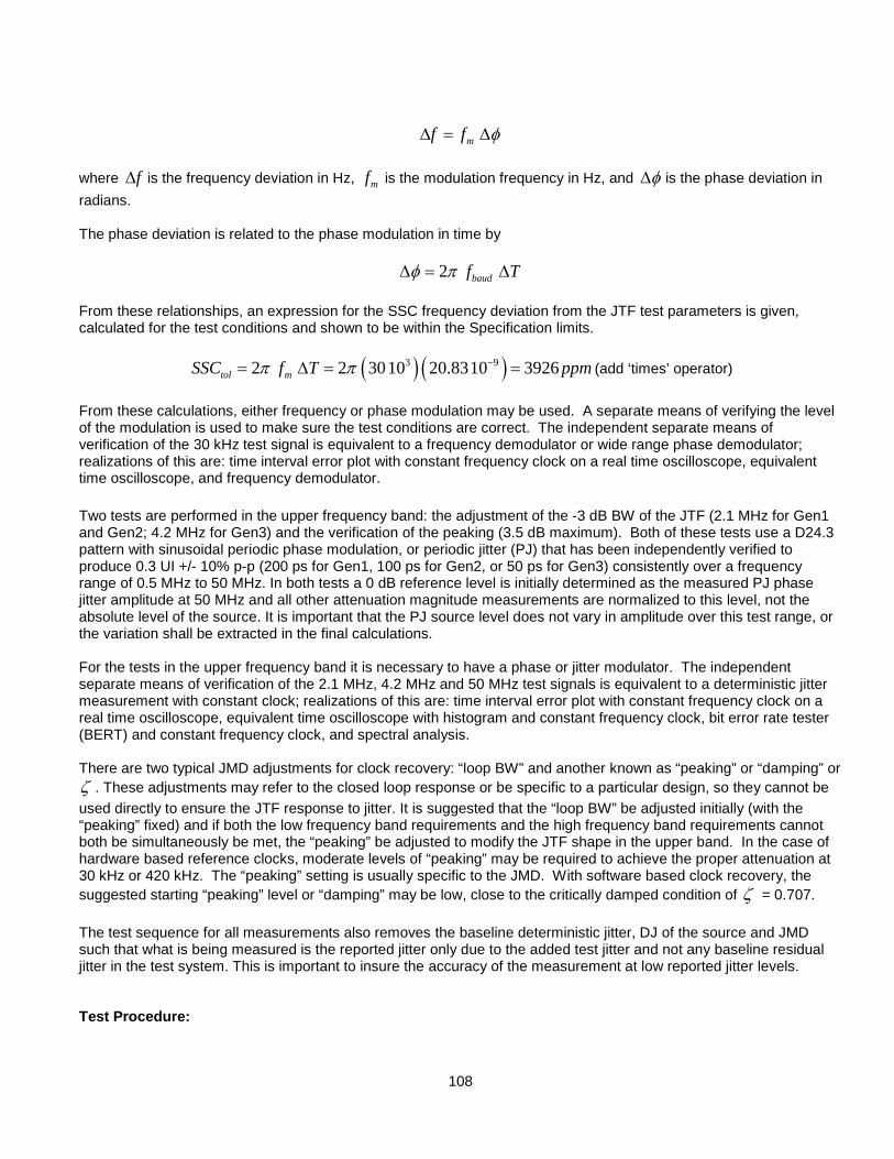
108
mf f φ∆ = ∆ where f∆ is the frequency deviation in Hz, mf is the modulation frequency in Hz, and φ∆ is the phase deviation in radians. The phase deviation is related to the phase modulation in time by
2 baudf Tφ π∆ = ∆ From these relationships, an expression for the SSC frequency deviation from the JTF test parameters is given, calculated for the test conditions and shown to be within the Specification limits.
( ) ( )3 92 2 3010 20.8310 3926tol mSSC f T ppmπ π −= ∆ = = (add ‘times’ operator)
From these calculations, either frequency or phase modulation may be used. A separate means of verifying the level of the modulation is used to make sure the test conditions are correct. The independent separate means of verification of the 30 kHz test signal is equivalent to a frequency demodulator or wide range phase demodulator; realizations of this are: time interval error plot with constant frequency clock on a real time oscilloscope, equivalent time oscilloscope, and frequency demodulator.
Two tests are performed in the upper frequency band: the adjustment of the -3 dB BW of the JTF (2.1 MHz for Gen1 and Gen2; 4.2 MHz for Gen3) and the verification of the peaking (3.5 dB maximum). Both of these tests use a D24.3 pattern with sinusoidal periodic phase modulation, or periodic jitter (PJ) that has been independently verified to produce 0.3 UI +/- 10% p-p (200 ps for Gen1, 100 ps for Gen2, or 50 ps for Gen3) consistently over a frequency range of 0.5 MHz to 50 MHz. In both tests a 0 dB reference level is initially determined as the measured PJ phase jitter amplitude at 50 MHz and all other attenuation magnitude measurements are normalized to this level, not the absolute level of the source. It is important that the PJ source level does not vary in amplitude over this test range, or the variation shall be extracted in the final calculations. For the tests in the upper frequency band it is necessary to have a phase or jitter modulator. The independent separate means of verification of the 2.1 MHz, 4.2 MHz and 50 MHz test signals is equivalent to a deterministic jitter measurement with constant clock; realizations of this are: time interval error plot with constant frequency clock on a real time oscilloscope, equivalent time oscilloscope with histogram and constant frequency clock, bit error rate tester (BERT) and constant frequency clock, and spectral analysis. There are two typical JMD adjustments for clock recovery: “loop BW” and another known as “peaking” or “damping” or ζ . These adjustments may refer to the closed loop response or be specific to a particular design, so they cannot be used directly to ensure the JTF response to jitter. It is suggested that the “loop BW” be adjusted initially (with the “peaking” fixed) and if both the low frequency band requirements and the high frequency band requirements cannot both be simultaneously be met, the “peaking” be adjusted to modify the JTF shape in the upper band. In the case of hardware based reference clocks, moderate levels of “peaking” may be required to achieve the proper attenuation at 30 kHz or 420 kHz. The “peaking” setting is usually specific to the JMD. With software based clock recovery, the suggested starting “peaking” level or “damping” may be low, close to the critically damped condition of ζ = 0.707. The test sequence for all measurements also removes the baseline deterministic jitter, DJ of the source and JMD such that what is being measured is the reported jitter only due to the added test jitter and not any baseline residual jitter in the test system. This is important to insure the accuracy of the measurement at low reported jitter levels. Test Procedure:
109
The response to jitter of the Jitter Measurement Device (JMD)(the reference clock is part of the JMD) is measured with three different jitter modulation frequencies corresponding to the three cases: 1) SSC (full tracking) 2) jitter (no tracking) 3) the boundary between SSC and jitter. The jitter source is independently verified by separate means. This ensures the jitter response of the JMD is reproducible across different test setups. The three Gen1 test signals are: 1) a 375 MHz +/- 0.035% square wave (which is a D24.3, 00110011 pattern) with rise time between 67 ps and 136 ps (20% to 80%) [1] with a sinusoidal phase modulation of 20.8 ns +/- 10% peak to peak at 30 kHz +/- 1%. 2) a 375 MHz square wave with a sinusoidal phase modulation of 200ps +/- 10% peak to peak at 50 MHz +/- 1%. 3) a 375 MHz square wave with no modulation.
The three Gen2 test signals are: 1) a 750 MHz +/- 0.035% square wave (which is a D24.3, 00110011 pattern) with rise time between 67 ps and 136 ps (20% to 80%) [1] with a sinusoidal phase modulation of 20.8 ns +/- 10% peak to peak at 30 kHz +/- 1%. 2) a 750 MHz square wave with a sinusoidal phase modulation of 100 ps +/- 10% peak to peak at 50 MHz +/- 1%. 3) a 750 MHz square wave with no modulation.
The three Gen3i test signals are: 1) a 1500 MHz +/- 0.035% square wave (which is a D24.3, 00110011 pattern) with rise time between 33 ps and 67 ps (20 to 80%) [1] with a sinusoidal phase modulation of 1.0 ns +/- 10% peak to peak at 420 kHz +/- 1%. 2) a 1500 MHz square wave with a sinusoidal phase modulation of 50 ps +/- 10% peak to peak at 50M Hz +/- 1%. 3) a 1500 MHz square wave with no modulation.
An independent separate means of verification of the test signals is used to make sure the level of the modulation is correct.
The test procedure checks two conditions: the JTF attenuation and the JTF bandwidth. Care is taken to minimize the number of absolute measurements taken, making most relative; this reduces the dependencies and improves accuracy.
1. For Gen 1 and Gen 2 calibration, adjust the pattern generator for a D24.3 pattern (00110011, with a rise time within specified limits) modulation to produce a 30 kHz +/- 1%, 20.8 ns p-p +/- 10% sinusoidal phase modulation For Gen3 calibration, adjust the pattern generator for a D24.3 pattern (00110011, with a rise time within specified limits) modulation to produce a 420 kHz +/- 1%, 1.0 ns p-p +/- 10% sinusoidal phase modulation.
2. Verify the level of modulation meets the requirements and record the p-p level, DJSSC. This is done with a Time Interval Error (TIE) type measurement or equivalent.
3. Apply test signal to the JMD. Turn off the sinusoidal phase modulation. Record the reported DJ, DJSSCOFF. 4. Turn on the sinusoidal phase modulation. Record the reported DJ, DJSSCON. 5. Calculate and record the level of measured DJ by subtracting the DJ with modulation off from DJ with
modulation on, DJMSSC = DJSSCON - DJSSCOFF. Calculate the jitter attenuation by 20Log(DJMSSC / DJSSC). This value shall fall within the range of –72 dB +/- 3 dB. Adjust the JMD settings to match this requirement.
• Adjust the pattern generator for a D24.3 pattern (00110011) and modulation to produce a 50 MHz +/-1%, 0.3 UI p-p +/- 10% (200 ps for Gen1,100 ps for Gen2, or 50 ps for Gen3i) sinusoidal phase modulation, also the COMP pattern. (SOF/HEADER/CRC/EOF)
• Contains leading X_RDY and trailing WTRM/SYNC/CONT primitives to maintain framing protocol consistency.
• Maintains running disparity. (Pattern begins and ends with the same running disparity, so that when it is transmitted continuously, the Monitoring Tool does not detect the leading SOF as a Running Disparity error.)
• Maintains desired ALIGN count and spacing. (First 2 Dwords are ALIGN out of every group of 256 Dwords.)
• Maintains ALIGN spacing upon wrapping. (Requires total pattern length to be an even multiple of 40*256=10240 bits. 92160=9*10240.)
• Overall pattern length is even multiple of 128/256/512 bits, for broad compatibility with known pattern generators.
Note that this pattern has been specifically designed for SATA-IO test purposes. Any deletion/insertion of
any symbol(s) other than align primitives or other modification to the exact bit sequence shall render the pattern invalid for the purposes of SATA-IO RSG testing.
110
Also note that the raw bit pattern is provided in an external .txt file, which may be downloaded from the SATA-IO website.)
4.1. SATA 3.0 ECN 009 Long FRAMED COMP Pattern 1: +K28.5- BC 1100000101 -D10.2- 4A 0101010101 -D10.2- 4A 0101010101 -D27.3+ 7B 1101100011 ALIGN (Repeat previous Dword until) 3: +D10.2+ 4A 0101010101 +D10.2+ 4A 0101010101 +D10.2+ 4A 0101010101 +D10.2+ 4A 0101010101 (Repeat previous Dword until) 10: +K28.3- 7C 1100001100 -D21.5- B5 1010101010 -D23.2+ 57 1110100101 +D23.2- 57 0001010101 X_RDY 11: -K28.3+ 7C 0011110011 +D21.5+ B5 1010101010 +D23.2- 57 0001010101 -D23.2+ 57 1110100101 X_RDY 12: +K28.3- 7C 1100001100 -D21.5- B5 1010101010 -D23.2+ 57 1110100101 +D23.2- 57 0001010101 X_RDY 13: -K28.3+ 7C 0011110011 +D21.5+ B5 1010101010 +D23.2- 57 0001010101 -D23.2+ 57 1110100101 X_RDY 14: +K28.3- 7C 1100001100 -D21.5- B5 1010101010 -D23.2+ 57 1110100101 +D23.2- 57 0001010101 X_RDY 15: -K28.3+ 7C 0011110011 +D21.5+ B5 1010101010 +D23.1- 37 0001011001 -D23.1+ 37 1110101001 SOF 16: +D11.6+ CB 1101000110 +D22.3+ 76 0110100011 +D18.6+ D2 0100110110 + D3.0- C2 0100100110 17: -D31.3+ 7F 1010110011 +D31.3- 7F 0101001100 -D31.3+ 7F 1010110011 +D31.3- 7F 0101001100 (Repeat previous Dword until) 257: -K28.5+ BC 0011111010 +D10.2+ 4A 0101010101 +D10.2+ 4A 0101010101 +D27.3- 7B 0010011100 ALIGN (Repeat previous Dword until) 259: -D31.3+ 7F 1010110011 +D31.3- 7F 0101001100 -D31.3+ 7F 1010110011 +D31.3- 7F 0101001100 (Repeat previous Dword until) 275: -D21.5- B5 1010101010 -D21.5- B5 1010101010 -D21.5- B5 1010101010 -D21.5- B5 1010101010 (Repeat previous Dword until) 339: -D24.3+ 78 1100110011 +D24.3- 78 0011001100 -D24.3+ 78 1100110011 +D24.3- 78 0011001100 (Repeat previous Dword until) 403: -D10.2- 4A 0101010101 -D10.2- 4A 0101010101 -D10.2- 4A 0101010101 -D10.2- 4A 0101010101 (Repeat previous Dword until) 467: -D25.6- D9 1001100110 - D6.1- 26 0110011001 -D25.6- D9 1001100110 - D6.1- 26 0110011001 (Repeat previous Dword until) 513: -K28.5+ BC 0011111010 +D10.2+ 4A 0101010101 +D10.2+ 4A 0101010101 +D27.3- 7B 0010011100 ALIGN (Repeat previous Dword until) 515: -D25.6- D9 1001100110 - D6.1- 26 0110011001 -D25.6- D9 1001100110 - D6.1- 26 0110011001 (Repeat previous Dword until) 533: -D17.7+ F1 1000110111 +D30.7+ FE 1000011110 + D7.1+ 27 0001111001 +D14.7- EE 0111001000 534: -D30.7- FE 0111100001 - D7.6- C7 1110000110 -D30.3+ 7E 0111100011 +D30.3- 7E 1000011100 535: -D30.3+ 7E 0111100011 +D30.3- 7E 1000011100 -D30.3+ 7E 0111100011 +D30.3- 7E 1000011100 (Repeat previous Dword until) 769: -K28.5+ BC 0011111010 +D10.2+ 4A 0101010101 +D10.2+ 4A 0101010101 +D27.3- 7B 0010011100 ALIGN (Repeat previous Dword until) 771: -D30.3+ 7E 0111100011 +D30.3- 7E 1000011100 -D30.3+ 7E 0111100011 +D30.3- 7E 1000011100 (Repeat previous Dword until) 1025: -K28.5+ BC 0011111010 +D10.2+ 4A 0101010101 +D10.2+ 4A 0101010101 +D27.3- 7B 0010011100 ALIGN (Repeat previous Dword until) 1027: -D30.3+ 7E 0111100011 +D30.3- 7E 1000011100 -D30.3+ 7E 0111100011 +D30.3- 7E 1000011100 (Repeat previous Dword until) 1048: - D3.7+ E3 1100011110 +D28.7- FC 0011100001 - D3.7+ E3 1100011110 +D28.7- FC 0011100001 1049: -D12.0+ 0C 0011011011 +D11.4- 8B 1101000010 -D12.0+ 0C 0011011011 +D11.3+ 6B 1101000011 LBPharvey 1050: +D12.0- 0C 0011010100 -D11.4+ 8B 1101001101 +D12.0- 0C 0011010100 -D11.3- 6B 1101001100 LBPharvey (Repeat previous ***2 Dwords*** until) 1281: -K28.5+ BC 0011111010 +D10.2+ 4A 0101010101 +D10.2+ 4A 0101010101 +D27.3- 7B 0010011100 ALIGN (Repeat previous Dword until) 1283: -D12.0+ 0C 0011011011 +D11.4- 8B 1101000010 -D12.0+ 0C 0011011011 +D11.3+ 6B 1101000011 LBPharvey 1284: +D12.0- 0C 0011010100 -D11.4+ 8B 1101001101 +D12.0- 0C 0011010100 -D11.3- 6B 1101001100 LBPharvey (Repeat previous ***2 Dwords*** until) 1307: -D20.2- 54 0010110101 -D20.2- 54 0010110101 -D20.2- 54 0010110101 -D20.2- 54 0010110101 (Repeat previous Dword until) 1537: -K28.5+ BC 0011111010 +D10.2+ 4A 0101010101 +D10.2+ 4A 0101010101 +D27.3- 7B 0010011100 ALIGN (Repeat previous Dword until) 1539: -D20.2- 54 0010110101 -D20.2- 54 0010110101 -D20.2- 54 0010110101 -D20.2- 54 0010110101 (Repeat previous Dword until) 1564: -D20.2- 54 0010110101 -D20.7+ F4 0010110111 +D11.5+ AB 1101001010 +D11.5+ AB 1101001010 1565: +D11.5+ AB 1101001010 +D11.5+ AB 1101001010 +D11.5+ AB 1101001010 +D11.5+ AB 1101001010 (Repeat previous Dword until) 1793: +K28.5- BC 1100000101 -D10.2- 4A 0101010101 -D10.2- 4A 0101010101 -D27.3+ 7B 1101100011 ALIGN (Repeat previous Dword until) 1795: +D11.5+ AB 1101001010 +D11.5+ AB 1101001010 +D11.5+ AB 1101001010 +D11.5+ AB 1101001010 (Repeat previous Dword until) 1822: +D11.5+ AB 1101001010 +D11.7- EB 1101001000 -D20.2- 54 0010110101 -D20.2- 54 0010110101 1823: -D21.5- B5 1010101010 -D21.5- B5 1010101010 -D21.5- B5 1010101010 -D21.5- B5 1010101010 (Repeat previous Dword until) 1887: -D24.3+ 78 1100110011 +D24.3- 78 0011001100 -D24.3+ 78 1100110011 +D24.3- 78 0011001100 (Repeat previous Dword until) 1951: -D10.2- 4A 0101010101 -D10.2- 4A 0101010101 -D10.2- 4A 0101010101 -D10.2- 4A 0101010101 (Repeat previous Dword until) 2015: -D25.6- D9 1001100110 - D6.1- 26 0110011001 -D25.6- D9 1001100110 - D6.1- 26 0110011001 (Repeat previous Dword until) 2049: -K28.5+ BC 0011111010 +D10.2+ 4A 0101010101 +D10.2+ 4A 0101010101 +D27.3- 7B 0010011100 ALIGN (Repeat previous Dword until) 2051: -D25.6- D9 1001100110 - D6.1- 26 0110011001 -D25.6- D9 1001100110 - D6.1- 26 0110011001
111
(Repeat previous Dword until) 2081: -D11.6- CB 1101000110 -D18.6- D2 0100110110 -D29.6+ DD 1011100110 + D6.4- 86 0110010010 2082: -K28.3+ 7C 0011110011 +D21.5+ B5 1010101010 +D21.6+ D5 1010100110 +D21.6+ D5 1010100110 EOF 2083: +K28.3- 7C 1100001100 -D21.5- B5 1010101010 -D24.2+ 58 1100110101 +D24.2- 58 0011000101 WTRM 2084: -K28.3+ 7C 0011110011 +D21.5+ B5 1010101010 +D24.2- 58 0011000101 -D24.2+ 58 1100110101 WTRM 2085: +K28.3- 7C 1100001100 -D21.5- B5 1010101010 -D24.2+ 58 1100110101 +D24.2- 58 0011000101 WTRM 2086: -K28.3+ 7C 0011110011 +D21.5+ B5 1010101010 +D24.2- 58 0011000101 -D24.2+ 58 1100110101 WTRM 2087: +K28.3- 7C 1100001100 -D21.4+ 95 1010101101 +D21.5+ B5 1010101010 +D21.5+ B5 1010101010 SYNC (Repeat previous Dword until) 2089: +K28.3- 7C 1100001100 -D10.5- AA 0101011010 -D25.4+ 99 1001101101 +D25.4- 99 1001100010 CONT 2090: -K28.3+ 7C 0011110011 +D10.5+ AA 0101011010 +D25.4- 99 1001100010 -D25.4+ 99 1001101101 CONT 2091: +D10.2+ 4A 0101010101 +D10.2+ 4A 0101010101 +D10.2+ 4A 0101010101 +D10.2+ 4A 0101010101 (Repeat previous Dword until) 2304: +D10.2+ 4A 0101010101 +D10.2+ 4A 0101010101 +D10.2+ 4A 0101010101 +D10.2+ 4A 0101010101
SATA-IO Confidential 111