service manual - especarchive.espec.ws/files/panasonic kx-ts2365rub_.pdf · service manual top next...
TRANSCRIPT

file:///C|/Documents and Settings/eDOK/Рабочий стол/KX-TS2365RUB.htm
Service Manual
TOP NEXT
ORDER NO. KM40305091C3
Telephone Equipment
KX-TS2365RUB
Integrated Telephone System
Black Version
(for Russia)
file:///C|/Documents and Settings/eDOK/Рабочий стол/KX-TS2365RUB.htm (1 of 2)11.02.2008 12:53:07

file:///C|/Documents and Settings/eDOK/Рабочий стол/KX-TS2365RUB.htm
© 2003 Panasonic Communications Co., Ltd. All rights reserved. Unauthorized copying and distribution is a violation of law.
TOP NEXT
file:///C|/Documents and Settings/eDOK/Рабочий стол/KX-TS2365RUB.htm (2 of 2)11.02.2008 12:53:07

http://202.224.189.179/view_new/OT/KX-TS2365RUB/SVC/2365rub.html
Table Of Contents
COVER
1 ABOUT LEAD FREE SOLDER (PbF: Pb free)
1.1 Suggested PbF Solder
1.2 How to recognize that Pb Free solder is used
2 FOR SERVICE TECHNICIANS
3 CAUTION
4 BATTERY
4.1 Installing the Batteries
4.2 Battery Replacement
5 LOCATION OF CONTROLS
6 DISPLAY
7 CONNECTION
7.1 Connecting the Handset/Telephone Line Cord
7.2 Connecting a Communication Device
8 SETTINGS
8.1 Selecting the Dialing Mode
8.2 Setting the PIN Code
8.3 Dial Lock
http://202.224.189.179/view_new/OT/KX-TS2365RUB/SVC/2365rub.html (1 of 4)11.02.2008 12:53:22
http://202.224.189.179/view_new/OT/KX-TS2365RUB/SVC/2365rub.html
8.3.1 To Set the Dial Lock
8.3.2 To Cancel the Dial Lock
8.4 Call Restriction
8.4.1 To Set the Call Restriction
8.5 How to Release the Establishment of Dial Lock
9 OPERATIONS
9.1 Making Calls
9.2 Answering Calls
9.3 FLASH Button
10 DISASSEMBLY INSTRUCTIONS
11 TROUBLE SHOOTING GUIDE
11.1 Service Hints
11.2 Pulse Dialing Problems
11.3 Tone Dialing Problems (Handset)
11.4 No Ringing Sound When Ring Signal is Input.
12 BLOCK DIAGRAM
13 CIRCUIT OPERATION
13.1 Bell Detector Circuit
13.2 Line Interface
http://202.224.189.179/view_new/OT/KX-TS2365RUB/SVC/2365rub.html (2 of 4)11.02.2008 12:53:22
http://202.224.189.179/view_new/OT/KX-TS2365RUB/SVC/2365rub.html
13.3 Speakerphone Circuit
13.3.1 Function
13.3.2 Circuit Operation
13.4 Telephone Line Interface
13.4.1 Circuit operation
13.5 Tone Detect
13.5.1 Circuit operation
13.6 Initializing Circuit
13.6.1 Function
13.6.2 Circuit operation
14 CPU DATA
14.1 IC801
15 HOW TO SET THE FLASH TIME AND REDIAL TIME
15.1 Flash Time
15.2 Redial Time
15.3 Speakerphone IC Data
16 BLOCK DIAGRAM (IC 1)
16.1 Communication ICs
17 MODULE BLOCK DIAGRAM
http://202.224.189.179/view_new/OT/KX-TS2365RUB/SVC/2365rub.html (3 of 4)11.02.2008 12:53:22
http://202.224.189.179/view_new/OT/KX-TS2365RUB/SVC/2365rub.html
17.1 MODULE BLOCK DIAGRAM
17.2 CONNECTOR PIN ASSIGNMENT
18 HOW TO REPLACE A FLAT PACKAGE IC
18.1 Preparation
18.2 Procedure
18.3 Removing Solder from Between Pins
19 TERMINAL GUIDE OF THE ICs, TRANSISTORS AND DIODES
20 CABINET AND ELECTRICAL PARTS LOCATION
21 ACCESSORY AND PACKING MATERIALS
22 REPLACEMENT PARTS LIST
22.1 Base Unit
22.1.1 Cabinet and Electrical Parts
22.1.2 Main P.C. Board Parts
22.2 ACCESSORIES AND PACKING MATERIALS
23 FOR SCHEMATIC DIAGRAM (SCHEMATIC DIAGRAM)
24 SCHEMATIC DIAGRAM
25 CIRCUIT BOARD
25.1 Component View
25.2 Flow Solder Side View
http://202.224.189.179/view_new/OT/KX-TS2365RUB/SVC/2365rub.html (4 of 4)11.02.2008 12:53:22
http://202.224.189.179/view_new/OT/KX-TS2365RUB/SVC/s0100000000x.html
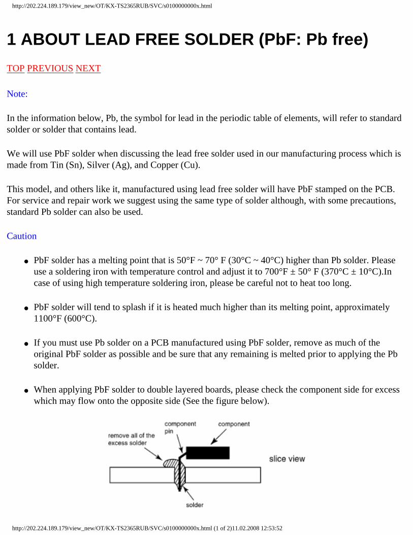
1 ABOUT LEAD FREE SOLDER (PbF: Pb free)
TOP PREVIOUS NEXT
Note:
In the information below, Pb, the symbol for lead in the periodic table of elements, will refer to standard solder or solder that contains lead.
We will use PbF solder when discussing the lead free solder used in our manufacturing process which is made from Tin (Sn), Silver (Ag), and Copper (Cu).
This model, and others like it, manufactured using lead free solder will have PbF stamped on the PCB. For service and repair work we suggest using the same type of solder although, with some precautions, standard Pb solder can also be used.
Caution
PbF solder has a melting point that is 50°F ~ 70° F (30°C ~ 40°C) higher than Pb solder. Please use a soldering iron with temperature control and adjust it to 700°F ± 50° F (370°C ± 10°C).In case of using high temperature soldering iron, please be careful not to heat too long.
PbF solder will tend to splash if it is heated much higher than its melting point, approximately 1100°F (600°C).
If you must use Pb solder on a PCB manufactured using PbF solder, remove as much of the original PbF solder as possible and be sure that any remaining is melted prior to applying the Pb solder.
When applying PbF solder to double layered boards, please check the component side for excess which may flow onto the opposite side (See the figure below).
http://202.224.189.179/view_new/OT/KX-TS2365RUB/SVC/s0100000000x.html (1 of 2)11.02.2008 12:53:52
http://202.224.189.179/view_new/OT/KX-TS2365RUB/SVC/s0100000000x.html
1.1 Suggested PbF Solder
1.2 How to recognize that Pb Free solder is used
TOP PREVIOUS NEXT
http://202.224.189.179/view_new/OT/KX-TS2365RUB/SVC/s0100000000x.html (2 of 2)11.02.2008 12:53:52
http://202.224.189.179/view_new/OT/KX-TS2365RUB/SVC/s0101000000.html
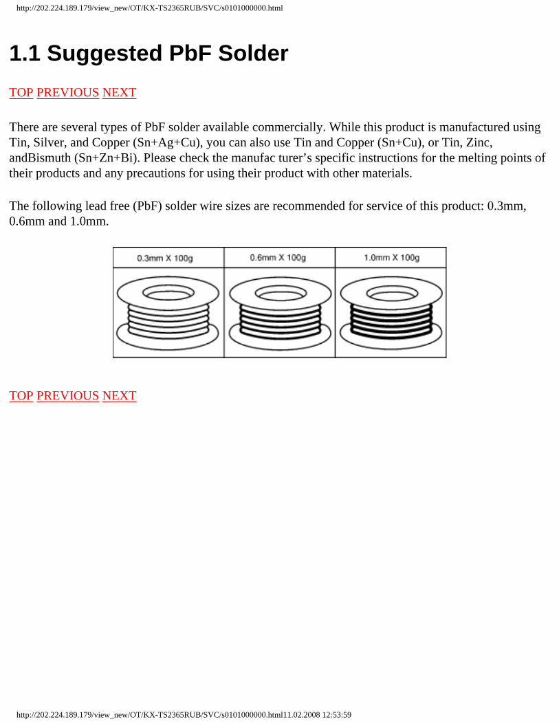
1.1 Suggested PbF Solder
TOP PREVIOUS NEXT
There are several types of PbF solder available commercially. While this product is manufactured using Tin, Silver, and Copper (Sn+Ag+Cu), you can also use Tin and Copper (Sn+Cu), or Tin, Zinc, andBismuth (Sn+Zn+Bi). Please check the manufac turer’s specific instructions for the melting points of their products and any precautions for using their product with other materials.
The following lead free (PbF) solder wire sizes are recommended for service of this product: 0.3mm, 0.6mm and 1.0mm.
TOP PREVIOUS NEXT
http://202.224.189.179/view_new/OT/KX-TS2365RUB/SVC/s0101000000.html11.02.2008 12:53:59

http://202.224.189.179/view_new/OT/KX-TS2365RUB/SVC/s0102000000.html
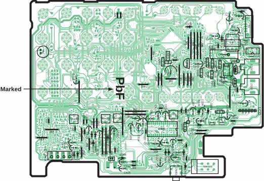
1.2 How to recognize that Pb Free solder is used
TOP PREVIOUS NEXT
(Flow Solder Side View)
TOP PREVIOUS NEXT
http://202.224.189.179/view_new/OT/KX-TS2365RUB/SVC/s0102000000.html11.02.2008 12:54:04
J56
J25
J63J64
J65
X801
X802
IC903
J26
J90J91
J61 J13
J60J69J62
J81
J92J93
R B Y G
H/S
_JAC
K
C401
VR401 VR402 VR901
VR601
J66
J57
C427
D107
D651
D104 LC
D
D106
J80
J10
D652
D601
D308
D421D
304
C302
C301
C414
J32
J30
J67
J68
J54
J55
J27
J22
J94
J84
J95
J96J97
J28J29J31
MIC
D307
R210
D302
D303
D422
C625
SPC618
C621C619
C651
R654
IC601
C308
J23
J82
J21
J52
D105
D3
J19
J83
J53
J18
C105
C101C102
C901
C202
J51
J50J14
J12
SW101J24
J20
C114
R194
R201
R101
J101
JJ101JJ102
R108
R191
R1
R192 J102
Q191
J35
J1
J34C1
C3
C6
C612
C611
C303
C652
J36
J15J16
J17Q
108E
C B
Q106
D2
T1
D101
Q102
Q104 Q
103
Q101
CN
401
C614
C617
C615
1415
281
C610
C106 C
191
C107
C2
S1
PC
1
R124
C601
C310
PO
101
SA
101
ECB
E C
B
E C
BE
C B
B C
E
B C
E
PbFMarked
http://202.224.189.179/view_new/OT/KX-TS2365RUB/SVC/s0200000000x.html
2 FOR SERVICE TECHNICIANS
TOP PREVIOUS NEXT
ICs and LSIs are vulnerable to static electricity.
When repairing, the following precautions will help prevent recurring malfunctions.
1. Cover plastic parts boxes with aluminum foil.
2. Ground the soldering irons.
3. Use a conductive mat on worktable.
4. Do not grasp IC or LSI pins with bare fingers.
TOP PREVIOUS NEXT
http://202.224.189.179/view_new/OT/KX-TS2365RUB/SVC/s0200000000x.html11.02.2008 12:54:17

http://202.224.189.179/view_new/OT/KX-TS2365RUB/SVC/s0300000000x.html
3 CAUTION
TOP PREVIOUS NEXT
Danger of explosion if battery is incorrectly replaced.
Replace only with the same or equivalent type recommended by the manufacturer.
Dispose of used batteries according to the manufacturer´s Instructions.
TOP PREVIOUS NEXT
http://202.224.189.179/view_new/OT/KX-TS2365RUB/SVC/s0300000000x.html11.02.2008 12:54:22
http://202.224.189.179/view_new/OT/KX-TS2365RUB/SVC/s0400000000x.html
4 BATTERY
TOP PREVIOUS NEXT
4.1 Installing the Batteries
4.2 Battery Replacement
TOP PREVIOUS NEXT
http://202.224.189.179/view_new/OT/KX-TS2365RUB/SVC/s0400000000x.html11.02.2008 12:54:26

http://202.224.189.179/view_new/OT/KX-TS2365RUB/SVC/s0401000000.html
4.1 Installing the Batteries
TOP PREVIOUS NEXT
TOP PREVIOUS NEXT
http://202.224.189.179/view_new/OT/KX-TS2365RUB/SVC/s0401000000.html11.02.2008 12:54:30
http://202.224.189.179/view_new/OT/KX-TS2365RUB/SVC/s0402000000.html
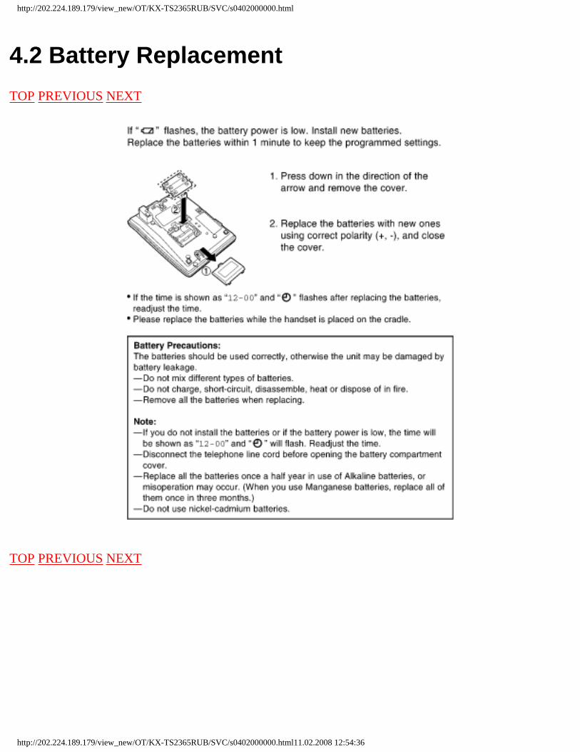
4.2 Battery Replacement
TOP PREVIOUS NEXT
TOP PREVIOUS NEXT
http://202.224.189.179/view_new/OT/KX-TS2365RUB/SVC/s0402000000.html11.02.2008 12:54:36
http://202.224.189.179/view_new/OT/KX-TS2365RUB/SVC/s0500000000x.html
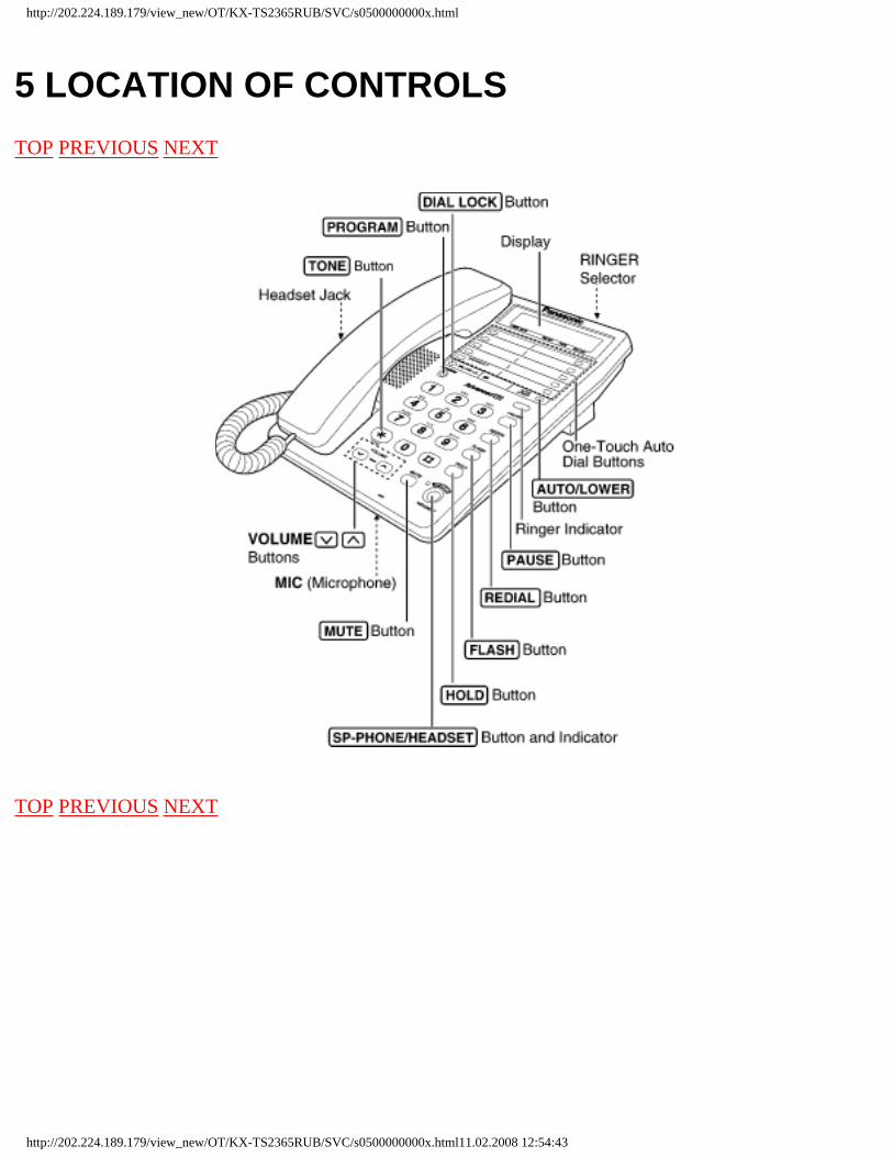
5 LOCATION OF CONTROLS
TOP PREVIOUS NEXT
TOP PREVIOUS NEXT
http://202.224.189.179/view_new/OT/KX-TS2365RUB/SVC/s0500000000x.html11.02.2008 12:54:43

http://202.224.189.179/view_new/OT/KX-TS2365RUB/SVC/s0600000000x.html
6 DISPLAY
TOP PREVIOUS NEXT
TOP PREVIOUS NEXT
http://202.224.189.179/view_new/OT/KX-TS2365RUB/SVC/s0600000000x.html11.02.2008 12:54:48
http://202.224.189.179/view_new/OT/KX-TS2365RUB/SVC/s0700000000x.html
7 CONNECTION
TOP PREVIOUS NEXT
7.1 Connecting the Handset/Telephone Line Cord
7.2 Connecting a Communication Device
TOP PREVIOUS NEXT
http://202.224.189.179/view_new/OT/KX-TS2365RUB/SVC/s0700000000x.html11.02.2008 12:54:52
http://202.224.189.179/view_new/OT/KX-TS2365RUB/SVC/s0701000000.html
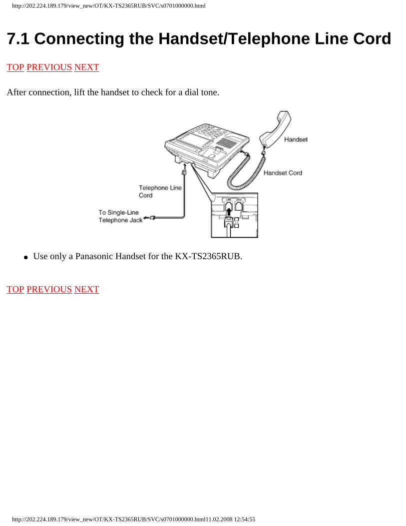
7.1 Connecting the Handset/Telephone Line Cord
TOP PREVIOUS NEXT
After connection, lift the handset to check for a dial tone.
Use only a Panasonic Handset for the KX-TS2365RUB.
TOP PREVIOUS NEXT
http://202.224.189.179/view_new/OT/KX-TS2365RUB/SVC/s0701000000.html11.02.2008 12:54:55

http://202.224.189.179/view_new/OT/KX-TS2365RUB/SVC/s0702000000.html
7.2 Connecting a Communication Device
TOP PREVIOUS NEXT
If you connect a communication device (computer, modem, fax, answering machine, etc.) to the telephone line, you can connect it through this unit using the DATA jack.
After connecting the handset and telephone line cord, connect the communication device telephone line cord to the DATA jack.
Make sure the communication device is not in use before using this unit (making calls, storing phone numbers in memory etc.) or the communication device may not operate properly.
TOP PREVIOUS NEXT
http://202.224.189.179/view_new/OT/KX-TS2365RUB/SVC/s0702000000.html11.02.2008 12:55:00

http://202.224.189.179/view_new/OT/KX-TS2365RUB/SVC/s0800000000x.html
8 SETTINGS
TOP PREVIOUS NEXT
8.1 Selecting the Dialing Mode
8.2 Setting the PIN Code
8.3 Dial Lock
8.3.1 To Set the Dial Lock
8.3.2 To Cancel the Dial Lock
8.4 Call Restriction
8.4.1 To Set the Call Restriction
8.5 How to Release the Establishment of Dial Lock
TOP PREVIOUS NEXT
http://202.224.189.179/view_new/OT/KX-TS2365RUB/SVC/s0800000000x.html11.02.2008 12:55:07
http://202.224.189.179/view_new/OT/KX-TS2365RUB/SVC/s0801000000.html
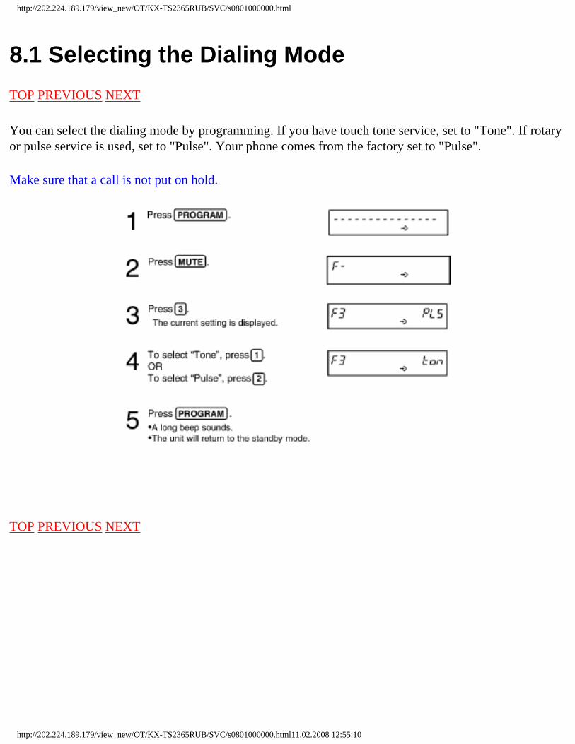
8.1 Selecting the Dialing Mode
TOP PREVIOUS NEXT
You can select the dialing mode by programming. If you have touch tone service, set to "Tone". If rotary or pulse service is used, set to "Pulse". Your phone comes from the factory set to "Pulse".
Make sure that a call is not put on hold.
TOP PREVIOUS NEXT
http://202.224.189.179/view_new/OT/KX-TS2365RUB/SVC/s0801000000.html11.02.2008 12:55:10
http://202.224.189.179/view_new/OT/KX-TS2365RUB/SVC/s0802000000.html
8.2 Setting the PIN Code
TOP PREVIOUS NEXT
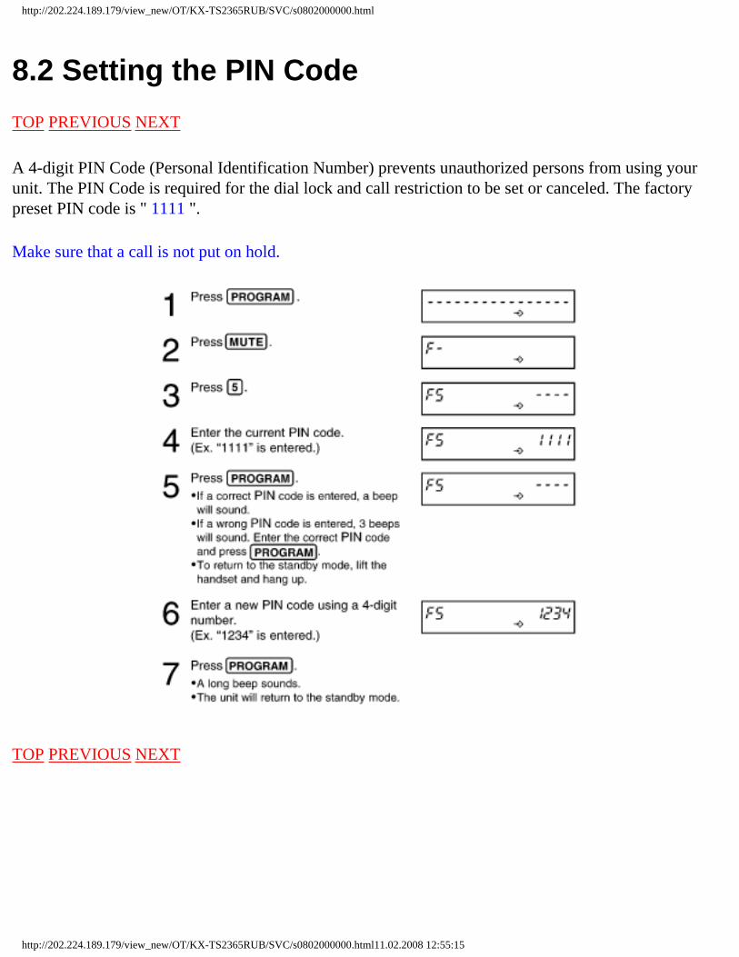
A 4-digit PIN Code (Personal Identification Number) prevents unauthorized persons from using your unit. The PIN Code is required for the dial lock and call restriction to be set or canceled. The factory preset PIN code is " 1111 ".
Make sure that a call is not put on hold.
TOP PREVIOUS NEXT
http://202.224.189.179/view_new/OT/KX-TS2365RUB/SVC/s0802000000.html11.02.2008 12:55:15
http://202.224.189.179/view_new/OT/KX-TS2365RUB/SVC/s0803000000.html
8.3 Dial Lock
TOP PREVIOUS NEXT
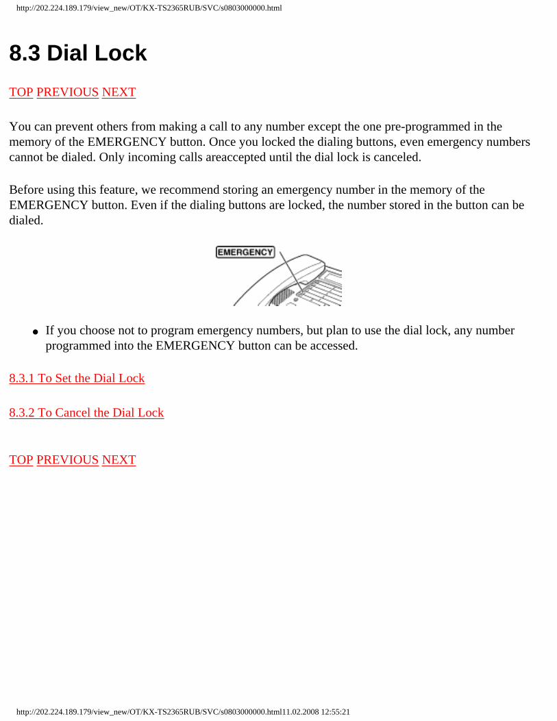
You can prevent others from making a call to any number except the one pre-programmed in the memory of the EMERGENCY button. Once you locked the dialing buttons, even emergency numbers cannot be dialed. Only incoming calls areaccepted until the dial lock is canceled.
Before using this feature, we recommend storing an emergency number in the memory of the EMERGENCY button. Even if the dialing buttons are locked, the number stored in the button can be dialed.
If you choose not to program emergency numbers, but plan to use the dial lock, any number programmed into the EMERGENCY button can be accessed.
8.3.1 To Set the Dial Lock
8.3.2 To Cancel the Dial Lock
TOP PREVIOUS NEXT
http://202.224.189.179/view_new/OT/KX-TS2365RUB/SVC/s0803000000.html11.02.2008 12:55:21
http://202.224.189.179/view_new/OT/KX-TS2365RUB/SVC/s0803010000.html
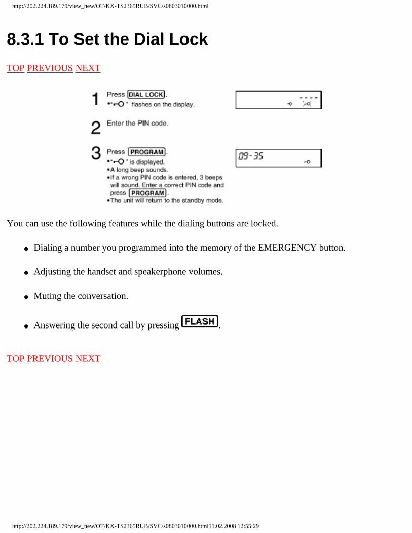
8.3.1 To Set the Dial Lock
TOP PREVIOUS NEXT
You can use the following features while the dialing buttons are locked.
Dialing a number you programmed into the memory of the EMERGENCY button.
Adjusting the handset and speakerphone volumes.
Muting the conversation.
Answering the second call by pressing .
TOP PREVIOUS NEXT
http://202.224.189.179/view_new/OT/KX-TS2365RUB/SVC/s0803010000.html11.02.2008 12:55:29
http://202.224.189.179/view_new/OT/KX-TS2365RUB/SVC/s0803020000.html
8.3.2 To Cancel the Dial Lock
TOP PREVIOUS NEXT
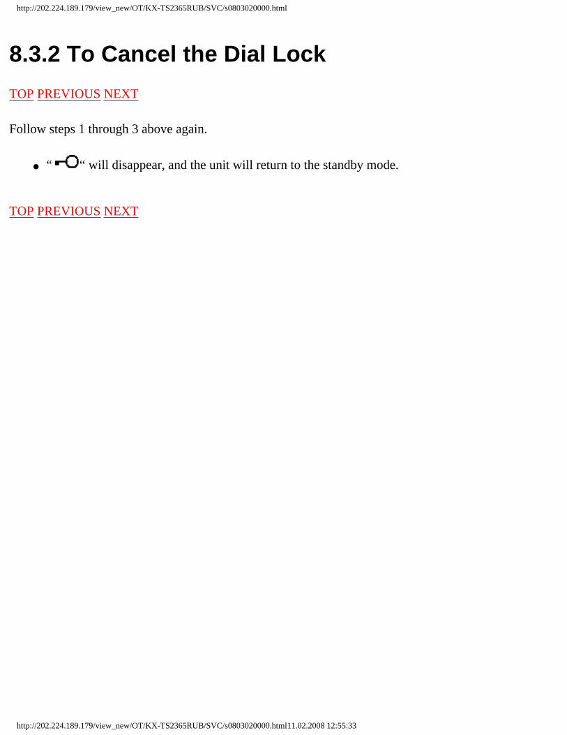
Follow steps 1 through 3 above again.
“ “ will disappear, and the unit will return to the standby mode.
TOP PREVIOUS NEXT
http://202.224.189.179/view_new/OT/KX-TS2365RUB/SVC/s0803020000.html11.02.2008 12:55:33
http://202.224.189.179/view_new/OT/KX-TS2365RUB/SVC/s0804000000.html
8.4 Call Restriction
TOP PREVIOUS NEXT
You can prevent the unit from dialing phone numbers beginning with specified digit(s) (1 digit or 2 digits). Phone numbers with the restricted leading digits cannot be dialed out.
8.4.1 To Set the Call Restriction
TOP PREVIOUS NEXT
http://202.224.189.179/view_new/OT/KX-TS2365RUB/SVC/s0804000000.html11.02.2008 12:55:42

http://202.224.189.179/view_new/OT/KX-TS2365RUB/SVC/s0804010000.html
8.4.1 To Set the Call Restriction
TOP PREVIOUS NEXT
Make sure that a call is not put on hold.
If your unit is connected to a PBX, this function may not operate. Contact your PBX supplier for more information.
When dialing a phone number with the restricted leading digit(s), the dialed number will flash on the display, but not dialed out.
TOP PREVIOUS NEXT
http://202.224.189.179/view_new/OT/KX-TS2365RUB/SVC/s0804010000.html11.02.2008 12:55:45

http://202.224.189.179/view_new/OT/KX-TS2365RUB/SVC/s0805000000.html
8.5 How to Release the Establishment of Dial Lock
TOP PREVIOUS NEXT
After this procedure, you will be able to establish a new password.
How to release the establishment of dial lock.
http://202.224.189.179/view_new/OT/KX-TS2365RUB/SVC/s0805000000.html (1 of 2)11.02.2008 12:55:52

http://202.224.189.179/view_new/OT/KX-TS2365RUB/SVC/s0805000000.html
TOP PREVIOUS NEXT
http://202.224.189.179/view_new/OT/KX-TS2365RUB/SVC/s0805000000.html (2 of 2)11.02.2008 12:55:52
http://202.224.189.179/view_new/OT/KX-TS2365RUB/SVC/s0900000000x.html
9 OPERATIONS
TOP PREVIOUS NEXT
9.1 Making Calls
9.2 Answering Calls
9.3 FLASH Button
TOP PREVIOUS NEXT
http://202.224.189.179/view_new/OT/KX-TS2365RUB/SVC/s0900000000x.html11.02.2008 12:56:02
http://202.224.189.179/view_new/OT/KX-TS2365RUB/SVC/s0901000000.html
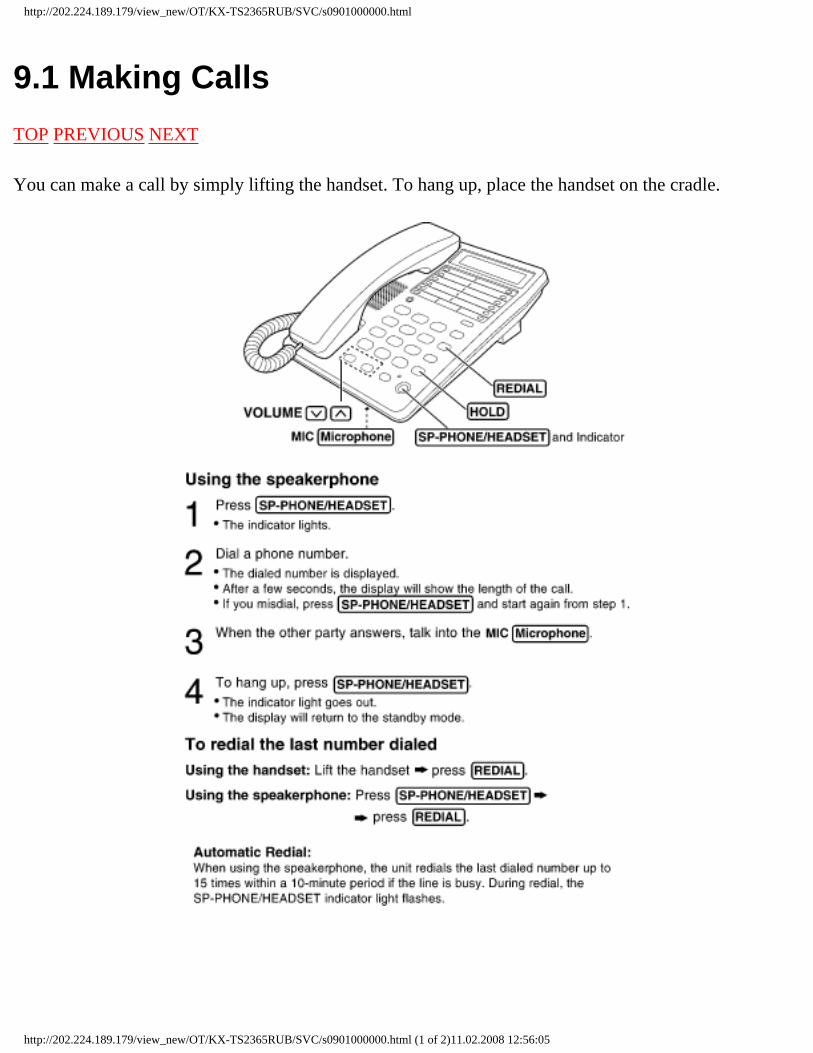
9.1 Making Calls
TOP PREVIOUS NEXT
You can make a call by simply lifting the handset. To hang up, place the handset on the cradle.
http://202.224.189.179/view_new/OT/KX-TS2365RUB/SVC/s0901000000.html (1 of 2)11.02.2008 12:56:05
http://202.224.189.179/view_new/OT/KX-TS2365RUB/SVC/s0901000000.html
TOP PREVIOUS NEXT
http://202.224.189.179/view_new/OT/KX-TS2365RUB/SVC/s0901000000.html (2 of 2)11.02.2008 12:56:05
http://202.224.189.179/view_new/OT/KX-TS2365RUB/SVC/s0902000000.html
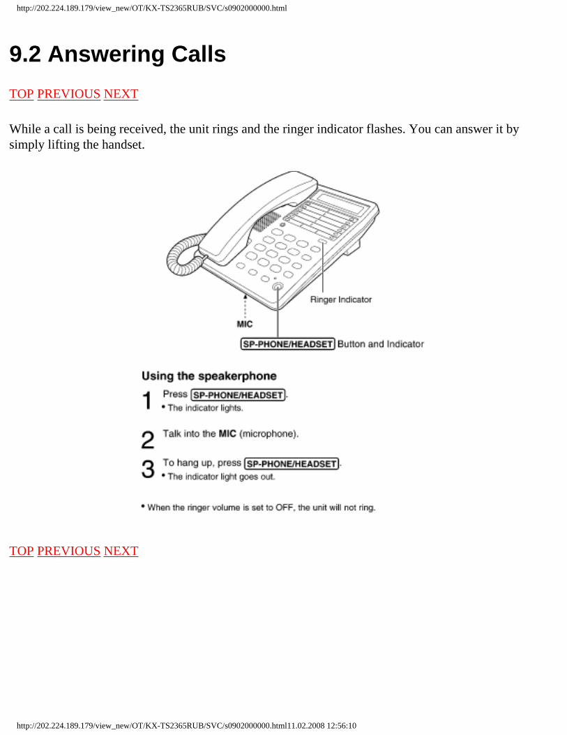
9.2 Answering Calls
TOP PREVIOUS NEXT
While a call is being received, the unit rings and the ringer indicator flashes. You can answer it by simply lifting the handset.
TOP PREVIOUS NEXT
http://202.224.189.179/view_new/OT/KX-TS2365RUB/SVC/s0902000000.html11.02.2008 12:56:10
http://202.224.189.179/view_new/OT/KX-TS2365RUB/SVC/s0903000000.html
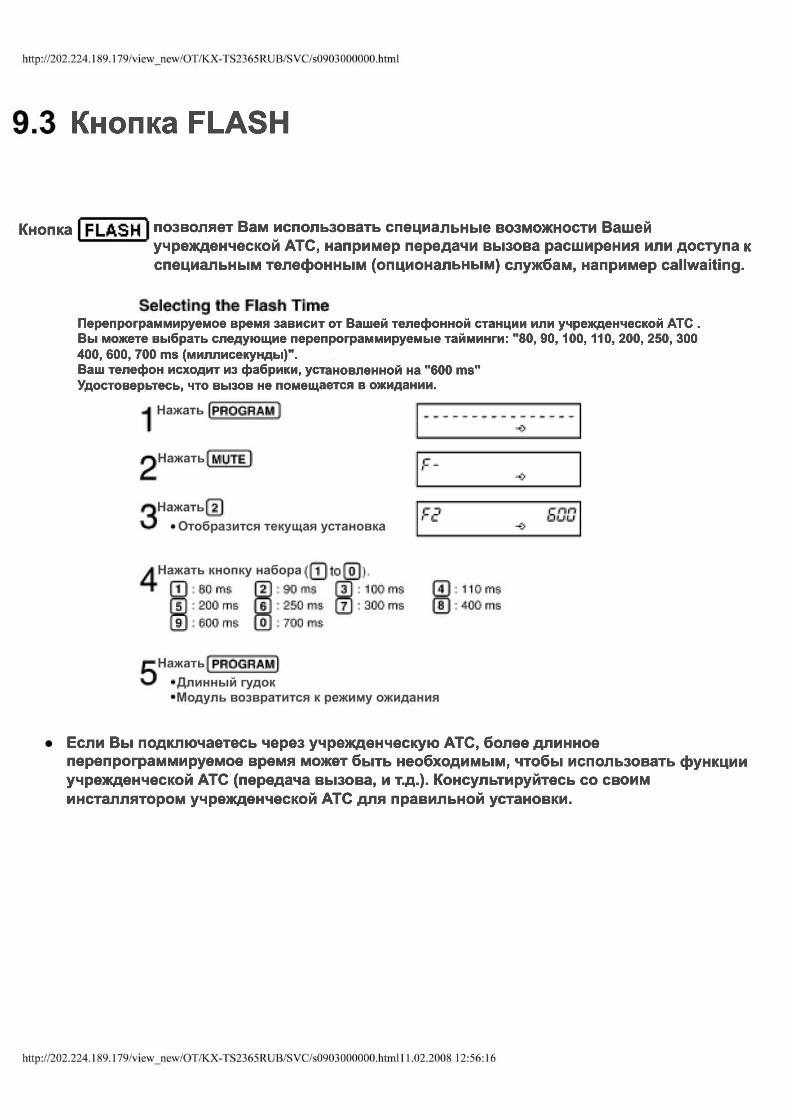
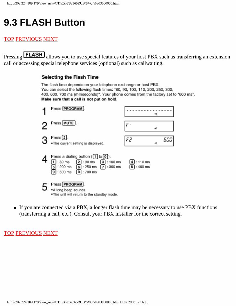
9.3 FLASH Button
TOP PREVIOUS NEXT
Pressing allows you to use special features of your host PBX such as transferring an extension call or accessing special telephone services (optional) such as callwaiting.
If you are connected via a PBX, a longer flash time may be necessary to use PBX functions (transferring a call, etc.). Consult your PBX installer for the correct setting.
TOP PREVIOUS NEXT
http://202.224.189.179/view_new/OT/KX-TS2365RUB/SVC/s0903000000.html11.02.2008 12:56:16

http://202.224.189.179/view_new/OT/KX-TS2365RUB/SVC/s1000000000x.html
10 DISASSEMBLY INSTRUCTIONS
TOP PREVIOUS NEXT
Shown in Fig -. To remove -. Remove -.
1 Lower Cabinet Screws (2.6×12) . . . . . . . . . . . . . (A)×5
2 Main P.C. Board The Main P.C.Board
TOP PREVIOUS NEXT
http://202.224.189.179/view_new/OT/KX-TS2365RUB/SVC/s1000000000x.html11.02.2008 12:56:26
http://202.224.189.179/view_new/OT/KX-TS2365RUB/SVC/s1100000000x.html
11 TROUBLE SHOOTING GUIDE
TOP PREVIOUS NEXT
11.1 Service Hints
11.2 Pulse Dialing Problems
11.3 Tone Dialing Problems (Handset)
11.4 No Ringing Sound When Ring Signal is Input.
TOP PREVIOUS NEXT
http://202.224.189.179/view_new/OT/KX-TS2365RUB/SVC/s1100000000x.html11.02.2008 12:56:30
http://202.224.189.179/view_new/OT/KX-TS2365RUB/SVC/s1101000000.html
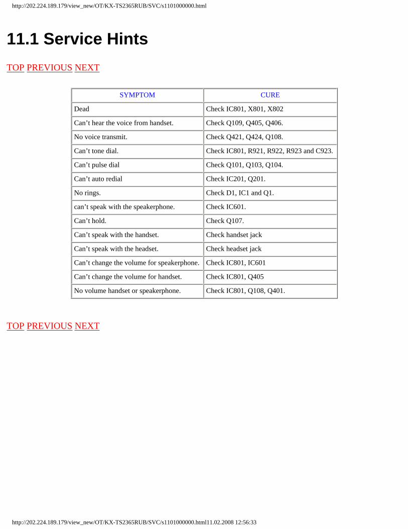
11.1 Service Hints
TOP PREVIOUS NEXT
SYMPTOM CURE
Dead Check IC801, X801, X802
Can’t hear the voice from handset. Check Q109, Q405, Q406.
No voice transmit. Check Q421, Q424, Q108.
Can’t tone dial. Check IC801, R921, R922, R923 and C923.
Can’t pulse dial Check Q101, Q103, Q104.
Can’t auto redial Check IC201, Q201.
No rings. Check D1, IC1 and Q1.
can’t speak with the speakerphone. Check IC601.
Can’t hold. Check Q107.
Can’t speak with the handset. Check handset jack
Can’t speak with the headset. Check headset jack
Can’t change the volume for speakerphone. Check IC801, IC601
Can’t change the volume for handset. Check IC801, Q405
No volume handset or speakerphone. Check IC801, Q108, Q401.
TOP PREVIOUS NEXT
http://202.224.189.179/view_new/OT/KX-TS2365RUB/SVC/s1101000000.html11.02.2008 12:56:33

http://202.224.189.179/view_new/OT/KX-TS2365RUB/SVC/s1102000000.html
11.2 Pulse Dialing Problems
TOP PREVIOUS NEXT
TOP PREVIOUS NEXT
http://202.224.189.179/view_new/OT/KX-TS2365RUB/SVC/s1102000000.html11.02.2008 12:56:39
http://202.224.189.179/view_new/OT/KX-TS2365RUB/SVC/s1103000000.html
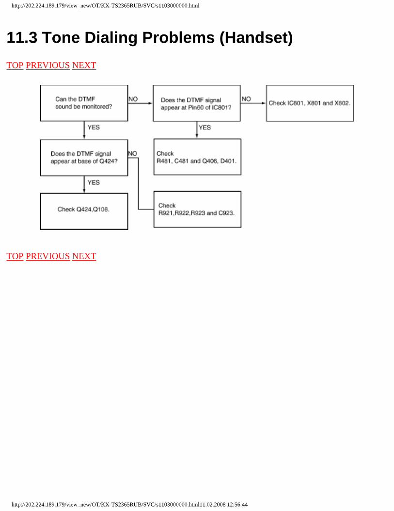
11.3 Tone Dialing Problems (Handset)
TOP PREVIOUS NEXT
TOP PREVIOUS NEXT
http://202.224.189.179/view_new/OT/KX-TS2365RUB/SVC/s1103000000.html11.02.2008 12:56:44
http://202.224.189.179/view_new/OT/KX-TS2365RUB/SVC/s1104000000.html
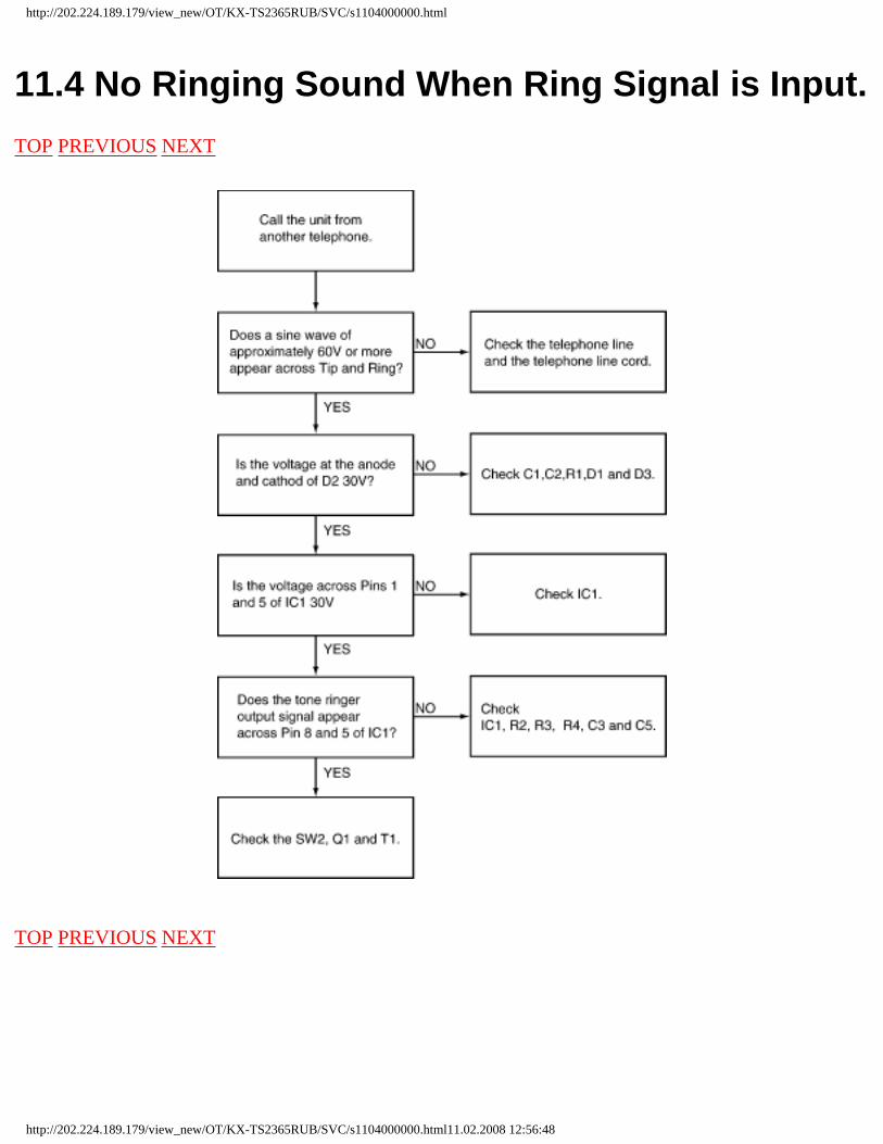
11.4 No Ringing Sound When Ring Signal is Input.
TOP PREVIOUS NEXT
TOP PREVIOUS NEXT
http://202.224.189.179/view_new/OT/KX-TS2365RUB/SVC/s1104000000.html11.02.2008 12:56:48
http://202.224.189.179/view_new/OT/KX-TS2365RUB/SVC/s1200000000b.html
12 BLOCK DIAGRAM
TOP PREVIOUS NEXT
TOP PREVIOUS NEXT
http://202.224.189.179/view_new/OT/KX-TS2365RUB/SVC/s1200000000b.html11.02.2008 12:56:57

Mic
Speaker
Head Set
LCD
IC801
IC601
Q421, Q424
CPU
HandsetAMP
Receiving
TransmitAMP
Dial
Q108
AMP
Q109Q405, Q406
T1
Q101, Q103
Ringer
D1
D101
IC201
IC1
HandsetAMP
Sending
ToneDetection
Mic
Speaker
Mic
Speaker
H/S
Data
TLINE
C1
R1
R
SP-PHONEAMP
Key Board Switch
KX-TS2365RUB: BLOCK DIAGRAM
IC303
Q302
CPU(Reset) IC304
3.7V
IC302
4.5V
Battery
BatteryLow
CPU
( (
http://202.224.189.179/view_new/OT/KX-TS2365RUB/SVC/s1300000000x.html
13 CIRCUIT OPERATION
TOP PREVIOUS NEXT
13.1 Bell Detector Circuit
13.2 Line Interface
13.3 Speakerphone Circuit
13.3.1 Function
13.3.2 Circuit Operation
13.4 Telephone Line Interface
13.4.1 Circuit operation
13.5 Tone Detect
13.5.1 Circuit operation
13.6 Initializing Circuit
13.6.1 Function
13.6.2 Circuit operation
TOP PREVIOUS NEXT
http://202.224.189.179/view_new/OT/KX-TS2365RUB/SVC/s1300000000x.html11.02.2008 12:57:05
http://202.224.189.179/view_new/OT/KX-TS2365RUB/SVC/s1301000000.html
13.1 Bell Detector Circuit
TOP PREVIOUS NEXT
When the bell signal is input between T/R, the signal are outputted at the speaker via the following path: Tel line → R1/C1 → D1 → Pin 1 of IC1 → Pin 8 of IC1 → C6 → T1 → C625 → Speaker
TOP PREVIOUS NEXT
http://202.224.189.179/view_new/OT/KX-TS2365RUB/SVC/s1301000000.html11.02.2008 12:57:09
http://202.224.189.179/view_new/OT/KX-TS2365RUB/SVC/s1302000000.html
13.2 Line Interface
TOP PREVIOUS NEXT
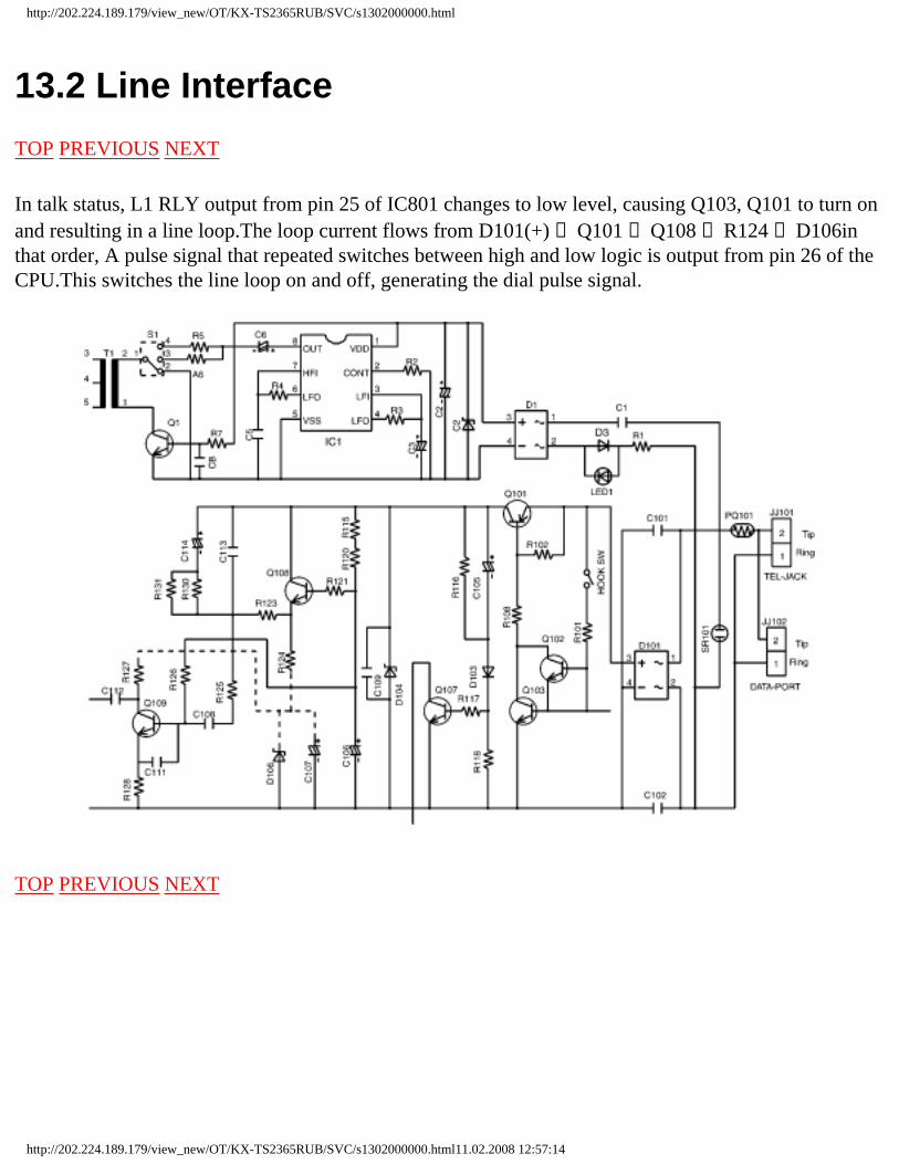
In talk status, L1 RLY output from pin 25 of IC801 changes to low level, causing Q103, Q101 to turn on and resulting in a line loop.The loop current flows from D101(+) → Q101 → Q108 → R124 → D106in that order, A pulse signal that repeated switches between high and low logic is output from pin 26 of the CPU.This switches the line loop on and off, generating the dial pulse signal.
TOP PREVIOUS NEXT
http://202.224.189.179/view_new/OT/KX-TS2365RUB/SVC/s1302000000.html11.02.2008 12:57:14
http://202.224.189.179/view_new/OT/KX-TS2365RUB/SVC/s1303000000.html
13.3 Speakerphone Circuit
TOP PREVIOUS NEXT
13.3.1 Function
13.3.2 Circuit Operation
TOP PREVIOUS NEXT
http://202.224.189.179/view_new/OT/KX-TS2365RUB/SVC/s1303000000.html11.02.2008 12:57:17
http://202.224.189.179/view_new/OT/KX-TS2365RUB/SVC/s1303010000.html
13.3.1 Function
TOP PREVIOUS NEXT
The circuit controls the automatic switching of the transmitted and received signals, to and from the telephone line, when the unit is used in the hands -free mode.
TOP PREVIOUS NEXT
http://202.224.189.179/view_new/OT/KX-TS2365RUB/SVC/s1303010000.html11.02.2008 12:57:24
http://202.224.189.179/view_new/OT/KX-TS2365RUB/SVC/s1303020000.html
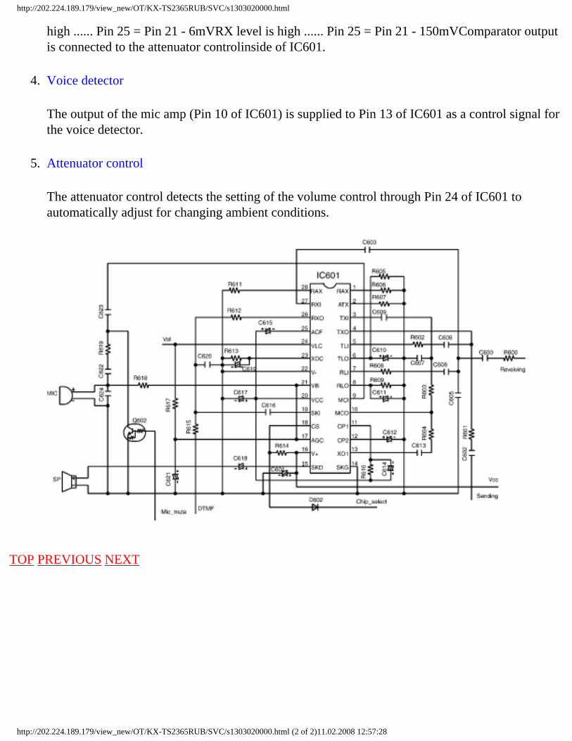
13.3.2 Circuit Operation
TOP PREVIOUS NEXT
The speakerphone can only provide a one-way communication path.
In other words, it can either transmit an outgoing signal or receive an incoming signal at a given time, but cannot do both simultaneously. Therefore, a switching circuit is necessary to control the flow of the outgoing and incoming signals.
This switching circuit is contained in IC601 and consists of a Voice Detector, TX Attenuator, RX Attenuator, Comparator and Attenuator Control. The circuit analyzes whether the TX(transmit) or the RX(receive) signal is louder, and then it processedthe signals such that the louder signal is given precedence.
The Voice Detector provides a DC input to the Attenuator Control corresponding to the TX signal.
The Comparator receives a TX and a RX signal, and supplies a DC input to the Attenuator Control corresponding to the RX signal.
The Attenuator Control provides a control signal to the TX and the RX attenuator to switch the appropriate signals on and off. The Attenuator Control also detects the level of the volume control to automatically adjust for changing ambient conditions.
1. Transmission signal path:
The input signal from the microphone is sent through the circuit via the following path:MIC → Pin 9 of IC601 → Pin 10 of IC601 → Pin 3 of IC601 → Pin 4 of IC601 → R601 → C602 → Q108 → Telline.
2. Reception signal path:
Signals receive from the telephone line are outputted at the speaker via the following path:Tel line → Q108 → Q109 → C112 → R600 → C603 → Pin 27 of IC601 → Pin 26 of IC601 → Pin19 of IC601 → Pin 15 of IC601 → Speaker.
3. Transmission/Reception switching
The comparison result between TX and RX outputs as a DC level of Pin 25 of IC601.TX level is
http://202.224.189.179/view_new/OT/KX-TS2365RUB/SVC/s1303020000.html (1 of 2)11.02.2008 12:57:28
http://202.224.189.179/view_new/OT/KX-TS2365RUB/SVC/s1303020000.html
high ...... Pin 25 = Pin 21 - 6mVRX level is high ...... Pin 25 = Pin 21 - 150mVComparator output is connected to the attenuator controlinside of IC601.
4. Voice detector
The output of the mic amp (Pin 10 of IC601) is supplied to Pin 13 of IC601 as a control signal for the voice detector.
5. Attenuator control
The attenuator control detects the setting of the volume control through Pin 24 of IC601 to automatically adjust for changing ambient conditions.
TOP PREVIOUS NEXT
http://202.224.189.179/view_new/OT/KX-TS2365RUB/SVC/s1303020000.html (2 of 2)11.02.2008 12:57:28
http://202.224.189.179/view_new/OT/KX-TS2365RUB/SVC/s1304000000.html
13.4 Telephone Line Interface
TOP PREVIOUS NEXT
13.4.1 Circuit operation
TOP PREVIOUS NEXT
http://202.224.189.179/view_new/OT/KX-TS2365RUB/SVC/s1304000000.html11.02.2008 12:57:35

http://202.224.189.179/view_new/OT/KX-TS2365RUB/SVC/s1304010000.html
13.4.1 Circuit operation
TOP PREVIOUS NEXT
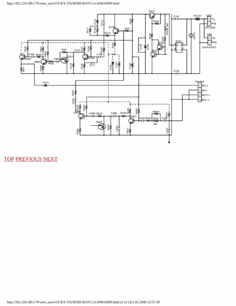
On hook
Q101 is open, Q101 is connected as to cut DC loop current and cut the voice signal.
Off hook
Q101 turns on thus providing an off-hook condition (active DC current flow through the circuit) and the following signal flow id for the DC loop current. T → POS101 → D101 → Q101 → Q108 → R124 → D106 → D101 → R
The receiving signal flows:
TEL line → POS101 → Q101 → C113 → R125 → C108 → Q109 → Q405 → Q406 → Speaker
The transmission signal flows
Mic → Q421 → Q424 → C435 → R437 → Q108 → Pos101 → Tel Line
http://202.224.189.179/view_new/OT/KX-TS2365RUB/SVC/s1304010000.html (1 of 2)11.02.2008 12:57:38
http://202.224.189.179/view_new/OT/KX-TS2365RUB/SVC/s1304010000.html
TOP PREVIOUS NEXT
http://202.224.189.179/view_new/OT/KX-TS2365RUB/SVC/s1304010000.html (2 of 2)11.02.2008 12:57:38

http://202.224.189.179/view_new/OT/KX-TS2365RUB/SVC/s1305000000.html
13.5 Tone Detect
TOP PREVIOUS NEXT
This circuit is used to sense the status of the line (busy tone or dial tone) during Auto Redial.
13.5.1 Circuit operation
TOP PREVIOUS NEXT
http://202.224.189.179/view_new/OT/KX-TS2365RUB/SVC/s1305000000.html11.02.2008 12:57:43
http://202.224.189.179/view_new/OT/KX-TS2365RUB/SVC/s1305010000.html
13.5.1 Circuit operation
TOP PREVIOUS NEXT
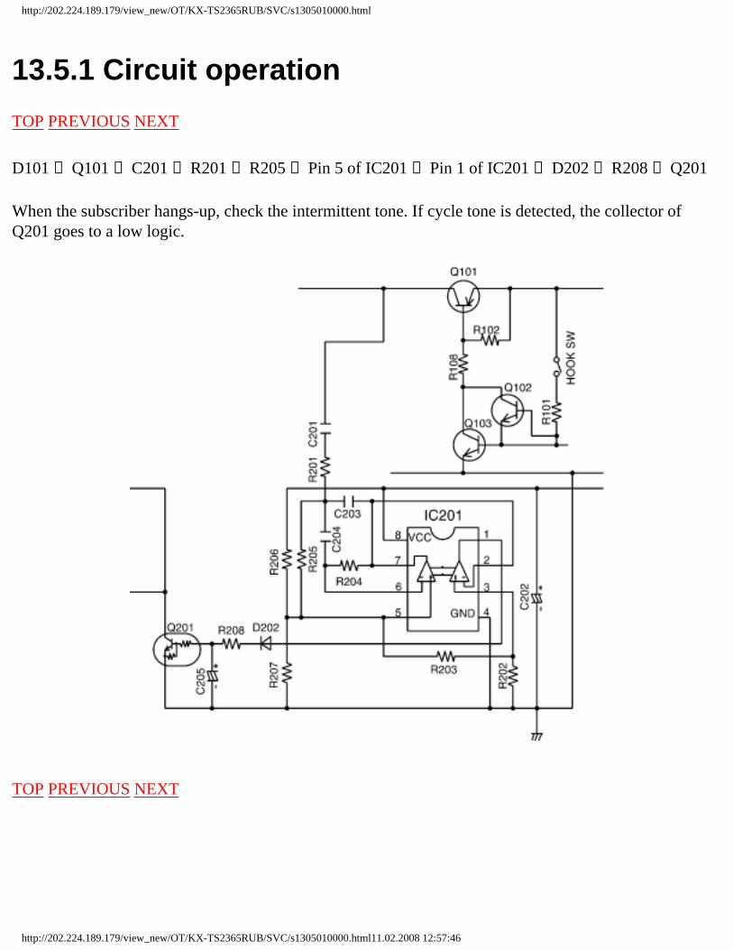
D101 → Q101 → C201 → R201 → R205 → Pin 5 of IC201 → Pin 1 of IC201 → D202 → R208 → Q201
When the subscriber hangs-up, check the intermittent tone. If cycle tone is detected, the collector of Q201 goes to a low logic.
TOP PREVIOUS NEXT
http://202.224.189.179/view_new/OT/KX-TS2365RUB/SVC/s1305010000.html11.02.2008 12:57:46
http://202.224.189.179/view_new/OT/KX-TS2365RUB/SVC/s1306000000.html
13.6 Initializing Circuit
TOP PREVIOUS NEXT
13.6.1 Function
13.6.2 Circuit operation
TOP PREVIOUS NEXT
http://202.224.189.179/view_new/OT/KX-TS2365RUB/SVC/s1306000000.html11.02.2008 12:57:51
http://202.224.189.179/view_new/OT/KX-TS2365RUB/SVC/s1306010000.html
13.6.1 Function
TOP PREVIOUS NEXT
This circuit is used to initialize the microcomputer when it incorporates batteries.
TOP PREVIOUS NEXT
http://202.224.189.179/view_new/OT/KX-TS2365RUB/SVC/s1306010000.html11.02.2008 12:57:54
http://202.224.189.179/view_new/OT/KX-TS2365RUB/SVC/s1306020000.html
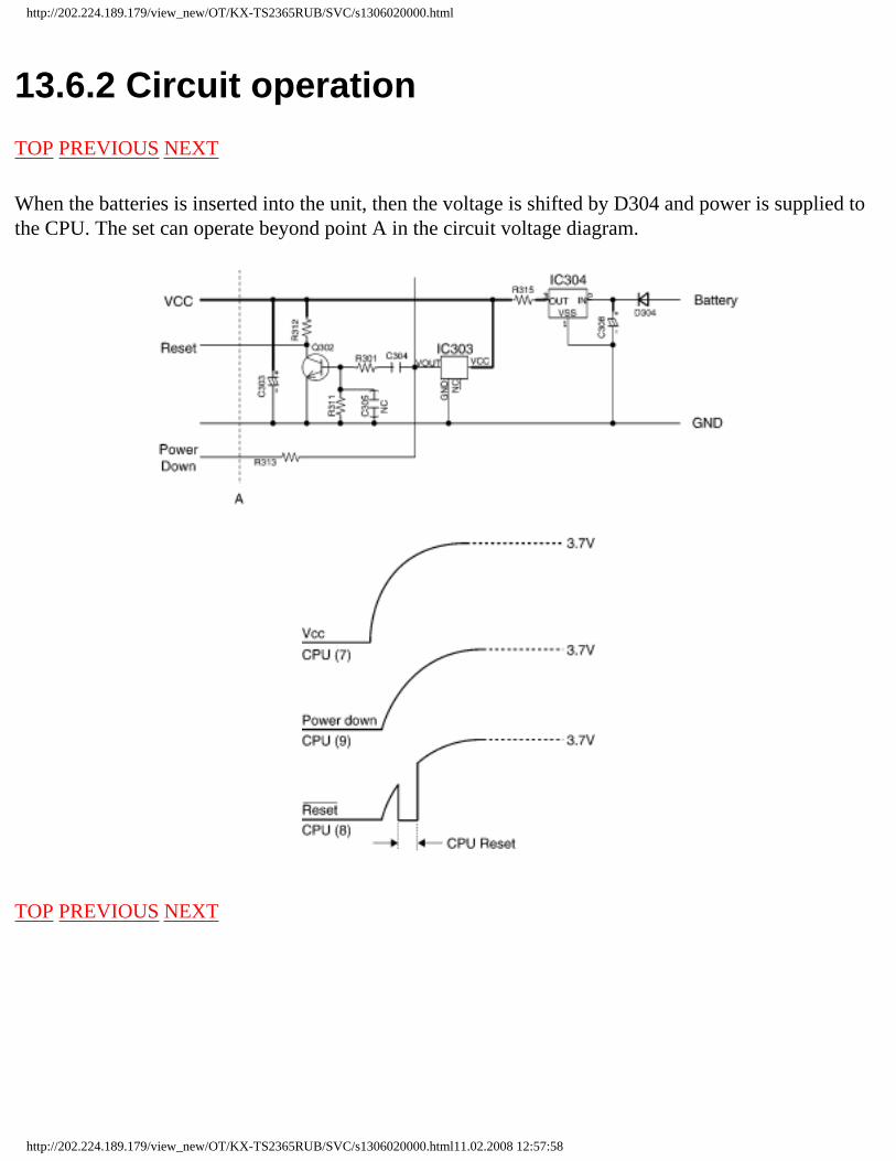
13.6.2 Circuit operation
TOP PREVIOUS NEXT
When the batteries is inserted into the unit, then the voltage is shifted by D304 and power is supplied to the CPU. The set can operate beyond point A in the circuit voltage diagram.
TOP PREVIOUS NEXT
http://202.224.189.179/view_new/OT/KX-TS2365RUB/SVC/s1306020000.html11.02.2008 12:57:58
http://202.224.189.179/view_new/OT/KX-TS2365RUB/SVC/s1400000000x.html
14 CPU DATA
TOP PREVIOUS NEXT
14.1 IC801
TOP PREVIOUS NEXT
http://202.224.189.179/view_new/OT/KX-TS2365RUB/SVC/s1400000000x.html11.02.2008 12:58:08

http://202.224.189.179/view_new/OT/KX-TS2365RUB/SVC/s1401000000.html
14.1 IC801
TOP PREVIOUS NEXT
TOP PREVIOUS NEXT
http://202.224.189.179/view_new/OT/KX-TS2365RUB/SVC/s1401000000.html11.02.2008 12:58:11
http://202.224.189.179/view_new/OT/KX-TS2365RUB/SVC/s1500000000x.html
15 HOW TO SET THE FLASH TIME AND REDIAL TIME
TOP PREVIOUS NEXT
*Refer to SCHEMATIC DIAGRAM ()
15.1 Flash Time
15.2 Redial Time
15.3 Speakerphone IC Data
TOP PREVIOUS NEXT
http://202.224.189.179/view_new/OT/KX-TS2365RUB/SVC/s1500000000x.html11.02.2008 12:58:17

http://202.224.189.179/view_new/OT/KX-TS2365RUB/SVC/s1501000000.html
15.1 Flash Time
TOP PREVIOUS NEXT
D901-D904 are used for default setting.
When you change the flash time, do the following procedure.
In case the program should be set frequency, change the default at D901-D904, then set the program.
0= Without
1= With
TOP PREVIOUS NEXT
http://202.224.189.179/view_new/OT/KX-TS2365RUB/SVC/s1501000000.html11.02.2008 12:58:27
http://202.224.189.179/view_new/OT/KX-TS2365RUB/SVC/s1502000000.html
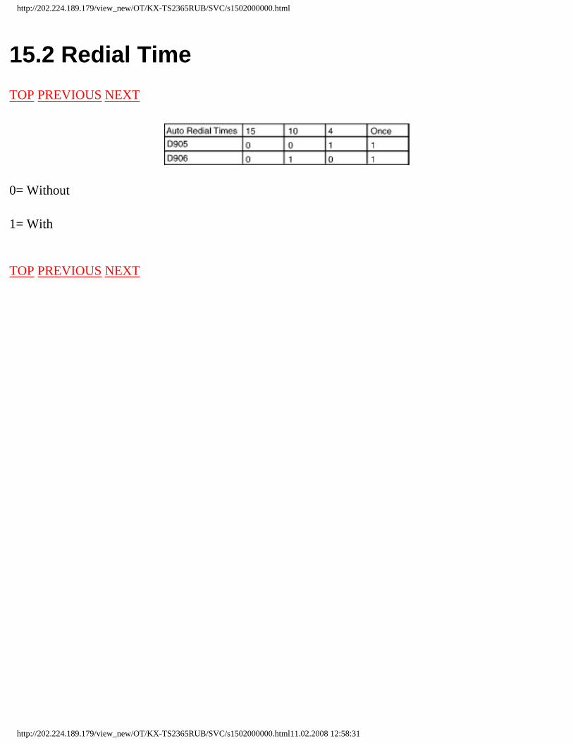
15.2 Redial Time
TOP PREVIOUS NEXT
0= Without
1= With
TOP PREVIOUS NEXT
http://202.224.189.179/view_new/OT/KX-TS2365RUB/SVC/s1502000000.html11.02.2008 12:58:31
http://202.224.189.179/view_new/OT/KX-TS2365RUB/SVC/s1503000000.html
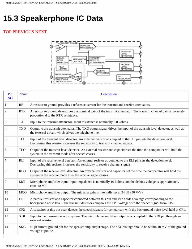
15.3 Speakerphone IC Data
TOP PREVIOUS NEXT
Pin NO.
Name Description
1 RR A resistor to ground provides a reference current for the transmit and receive attenuators.
2 RTX A resistor to ground determines the nominal gain of the transmit attenuator. The transmit channel gain is inversely proportional to the RTX resistance.
3 TXI Input to the transmit attenuator. Input resistance is nominally 5.0 kohms.
4 TXO Output to the transmit attenuator. The TXO output signal drives the input of the transmit level detector, as well as the external circuit which drives the telephone line.
5 TLI Input of the transmit level detector. An external resistor ac coupled to the TLI pin sets the detection level. Decreasing this resistor increases the sensitivity to transmit channel signals.
6 TLO Output of the transmit level detector. An external resistor and capacitor set the time the comparator will hold the system in the transmit mode after speech ceases.
7 RLI Input of the receive level detector. An external resistor ac coupled to the RLI pin sets the detection level. Decreasing this resistor increases the sensitivity to receive channel signals.
8 RLO Output of the receive level detector. An external resistor and capacitor set the time the comparator will hold the system in the receive mode after the receive signal ceases.
9 MCI Microphone amplifier input. Input impedance is nominally 10 kohms and the dc bias voltage is approximately equal to VB.
10 MCO Microphone amplifier output. The mic amp gain is internally set at 34 dB (50 V/V).
11 CP1 A parallel resistor and capacitor connected between this pin and Vcc holds a voltage corresponding to the background noise level. The transmit detector compares the CP1 voltage with the speech signal from CP2.
12 CP2 A capacitor at this pin peak detects the speech signals for comparison with the background noise level held at CP1.
13 XDI Input to the transmit detector system. The microphone amplifier output is ac coupled to the XDI pin through an external resistor.
14 SKG High current ground pin for the speaker amp output stage. The SKG voltage should be within 10 mV of the ground voltage at pin 22.
http://202.224.189.179/view_new/OT/KX-TS2365RUB/SVC/s1503000000.html (1 of 2)11.02.2008 12:58:35
http://202.224.189.179/view_new/OT/KX-TS2365RUB/SVC/s1503000000.html
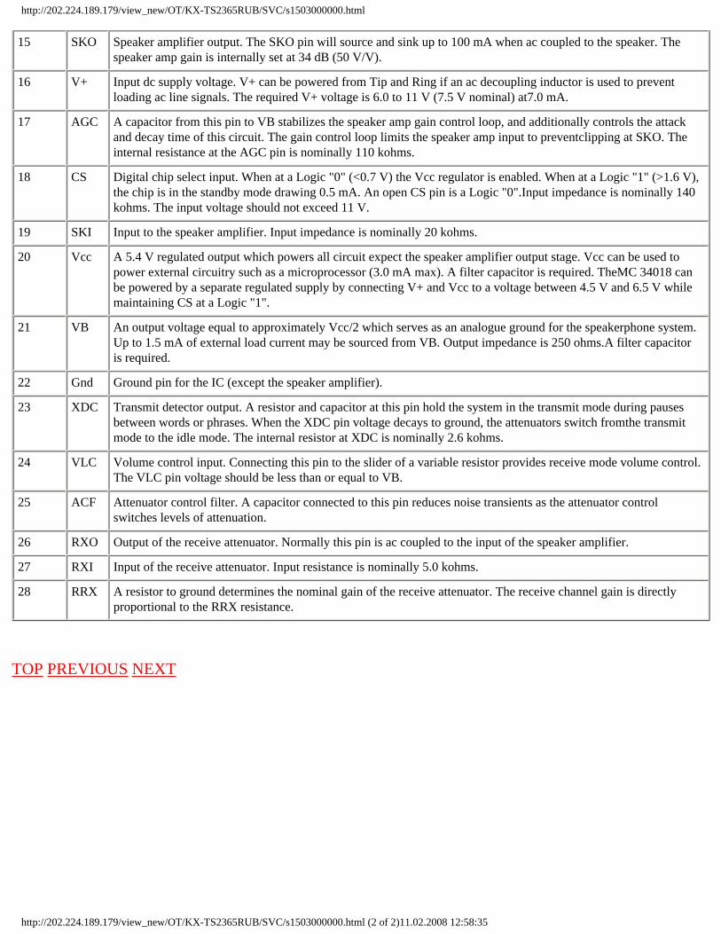
15 SKO Speaker amplifier output. The SKO pin will source and sink up to 100 mA when ac coupled to the speaker. The speaker amp gain is internally set at 34 dB (50 V/V).
16 V+ Input dc supply voltage. V+ can be powered from Tip and Ring if an ac decoupling inductor is used to prevent loading ac line signals. The required V+ voltage is 6.0 to 11 V (7.5 V nominal) at7.0 mA.
17 AGC A capacitor from this pin to VB stabilizes the speaker amp gain control loop, and additionally controls the attack and decay time of this circuit. The gain control loop limits the speaker amp input to preventclipping at SKO. The internal resistance at the AGC pin is nominally 110 kohms.
18 CS Digital chip select input. When at a Logic "0" (<0.7 V) the Vcc regulator is enabled. When at a Logic "1" (>1.6 V), the chip is in the standby mode drawing 0.5 mA. An open CS pin is a Logic "0".Input impedance is nominally 140 kohms. The input voltage should not exceed 11 V.
19 SKI Input to the speaker amplifier. Input impedance is nominally 20 kohms.
20 Vcc A 5.4 V regulated output which powers all circuit expect the speaker amplifier output stage. Vcc can be used to power external circuitry such as a microprocessor (3.0 mA max). A filter capacitor is required. TheMC 34018 can be powered by a separate regulated supply by connecting V+ and Vcc to a voltage between 4.5 V and 6.5 V while maintaining CS at a Logic "1".
21 VB An output voltage equal to approximately Vcc/2 which serves as an analogue ground for the speakerphone system. Up to 1.5 mA of external load current may be sourced from VB. Output impedance is 250 ohms.A filter capacitor is required.
22 Gnd Ground pin for the IC (except the speaker amplifier).
23 XDC Transmit detector output. A resistor and capacitor at this pin hold the system in the transmit mode during pauses between words or phrases. When the XDC pin voltage decays to ground, the attenuators switch fromthe transmit mode to the idle mode. The internal resistor at XDC is nominally 2.6 kohms.
24 VLC Volume control input. Connecting this pin to the slider of a variable resistor provides receive mode volume control. The VLC pin voltage should be less than or equal to VB.
25 ACF Attenuator control filter. A capacitor connected to this pin reduces noise transients as the attenuator control switches levels of attenuation.
26 RXO Output of the receive attenuator. Normally this pin is ac coupled to the input of the speaker amplifier.
27 RXI Input of the receive attenuator. Input resistance is nominally 5.0 kohms.
28 RRX A resistor to ground determines the nominal gain of the receive attenuator. The receive channel gain is directly proportional to the RRX resistance.
TOP PREVIOUS NEXT
http://202.224.189.179/view_new/OT/KX-TS2365RUB/SVC/s1503000000.html (2 of 2)11.02.2008 12:58:35
http://202.224.189.179/view_new/OT/KX-TS2365RUB/SVC/s1600000000x.html
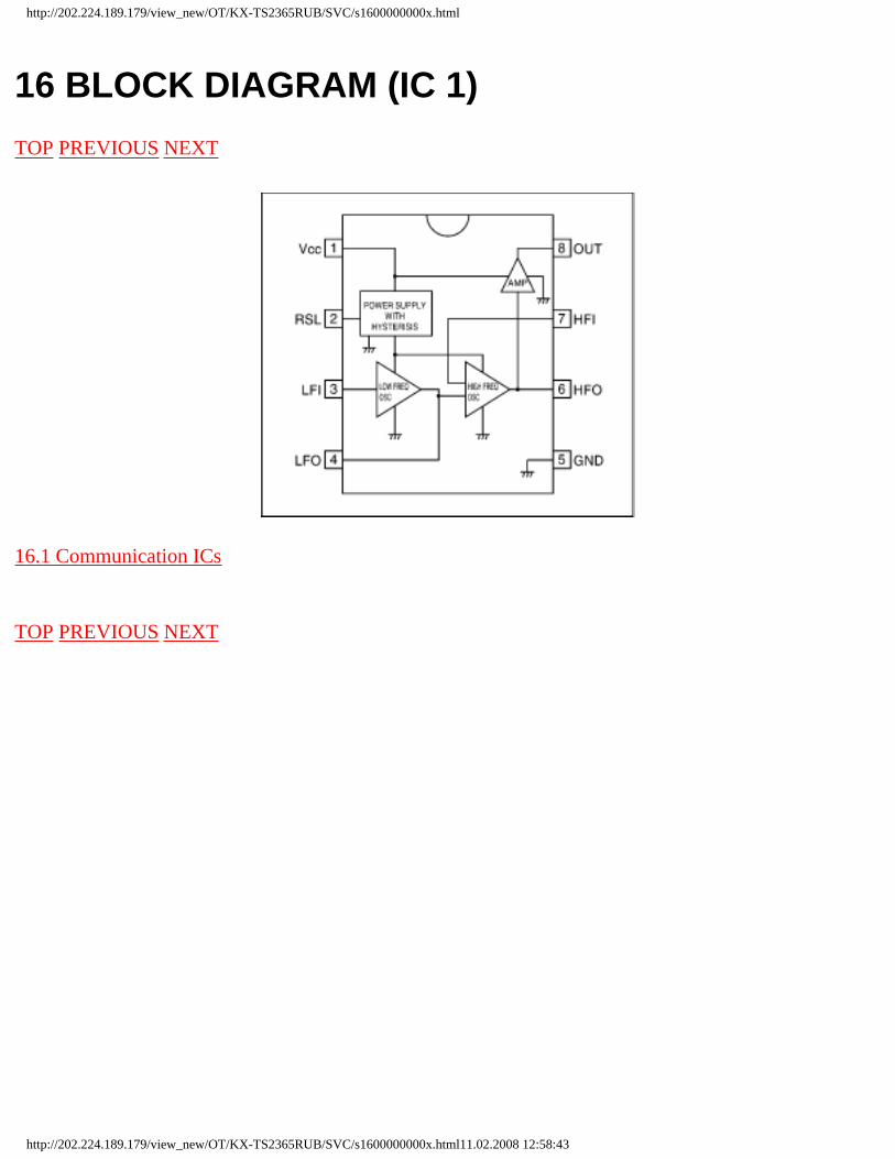
16 BLOCK DIAGRAM (IC 1)
TOP PREVIOUS NEXT
16.1 Communication ICs
TOP PREVIOUS NEXT
http://202.224.189.179/view_new/OT/KX-TS2365RUB/SVC/s1600000000x.html11.02.2008 12:58:43

http://202.224.189.179/view_new/OT/KX-TS2365RUB/SVC/s1601000000.html
16.1 Communication ICs
TOP PREVIOUS NEXT
TOP PREVIOUS NEXT
http://202.224.189.179/view_new/OT/KX-TS2365RUB/SVC/s1601000000.html11.02.2008 12:58:46
http://202.224.189.179/view_new/OT/KX-TS2365RUB/SVC/s1700000000x.html
17 MODULE BLOCK DIAGRAM
TOP PREVIOUS NEXT
17.1 MODULE BLOCK DIAGRAM
17.2 CONNECTOR PIN ASSIGNMENT
TOP PREVIOUS NEXT
http://202.224.189.179/view_new/OT/KX-TS2365RUB/SVC/s1700000000x.html11.02.2008 12:58:51

http://202.224.189.179/view_new/OT/KX-TS2365RUB/SVC/s1701000000.html
17.1 MODULE BLOCK DIAGRAM
TOP PREVIOUS NEXT
TOP PREVIOUS NEXT
http://202.224.189.179/view_new/OT/KX-TS2365RUB/SVC/s1701000000.html11.02.2008 12:58:54

http://202.224.189.179/view_new/OT/KX-TS2365RUB/SVC/s1702000000.html
17.2 CONNECTOR PIN ASSIGNMENT
TOP PREVIOUS NEXT
Pin no.
signal Function Enable
1 VDD Power Supply (5V) -
2 VLCD LCD Power Input -
3 VSS Power Gnd (0V) -
4 DATA Serial Data Input H/L
5 WR Write Data H, L → L
6 CS Chip Selection H, L → H
TOP PREVIOUS NEXT
http://202.224.189.179/view_new/OT/KX-TS2365RUB/SVC/s1702000000.html11.02.2008 12:58:59
http://202.224.189.179/view_new/OT/KX-TS2365RUB/SVC/s1800000000x.html
18 HOW TO REPLACE A FLAT PACKAGE IC
TOP PREVIOUS NEXT
18.1 Preparation
18.2 Procedure
18.3 Removing Solder from Between Pins
TOP PREVIOUS NEXT
http://202.224.189.179/view_new/OT/KX-TS2365RUB/SVC/s1800000000x.html11.02.2008 12:59:09
http://202.224.189.179/view_new/OT/KX-TS2365RUB/SVC/s1801000000.html
18.1 Preparation
TOP PREVIOUS NEXT
PbF (: Pb free) Solder
Soldering Iron
Tip Temperature of 700°F ± 50°F (370°C ± 10°C)
Note: We recommend a 30 to 40 Watt soldering iron. An expert may be able to use a 60 to 80 Watt iron where someone with less experience could overheat and damage the PCB foil.
Flux
Recommended Flux: Specific Gravity → 0.82.
Type → RMA (lower residue, non-cleaning type)
Note: See ABOUT LEAD FREE SOLDER (PbF: Pb free) ().
TOP PREVIOUS NEXT
http://202.224.189.179/view_new/OT/KX-TS2365RUB/SVC/s1801000000.html11.02.2008 12:59:11

http://202.224.189.179/view_new/OT/KX-TS2365RUB/SVC/s1802000000.html
18.2 Procedure
TOP PREVIOUS NEXT
1. Tack the flat pack IC to the PCB by temporarily soldering two diagonally opposite pins in the correct positions on the PCB.
Be certain each pin is located over the correct pad on the PCB.
2. Apply flux to all of the pins on the IC.
3. Being careful to not unsolder the tack points, slide the soldering iron along the tips of the pins while feeding enough solder to the tip so that it flows under the pins as they are heated.
TOP PREVIOUS NEXT
http://202.224.189.179/view_new/OT/KX-TS2365RUB/SVC/s1802000000.html11.02.2008 12:59:16
http://202.224.189.179/view_new/OT/KX-TS2365RUB/SVC/s1803000000.html
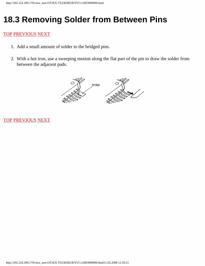
18.3 Removing Solder from Between Pins
TOP PREVIOUS NEXT
1. Add a small amount of solder to the bridged pins.
2. With a hot iron, use a sweeping motion along the flat part of the pin to draw the solder from between the adjacent pads.
TOP PREVIOUS NEXT
http://202.224.189.179/view_new/OT/KX-TS2365RUB/SVC/s1803000000.html11.02.2008 12:59:21
http://202.224.189.179/view_new/OT/KX-TS2365RUB/SVC/s1900000000x.html
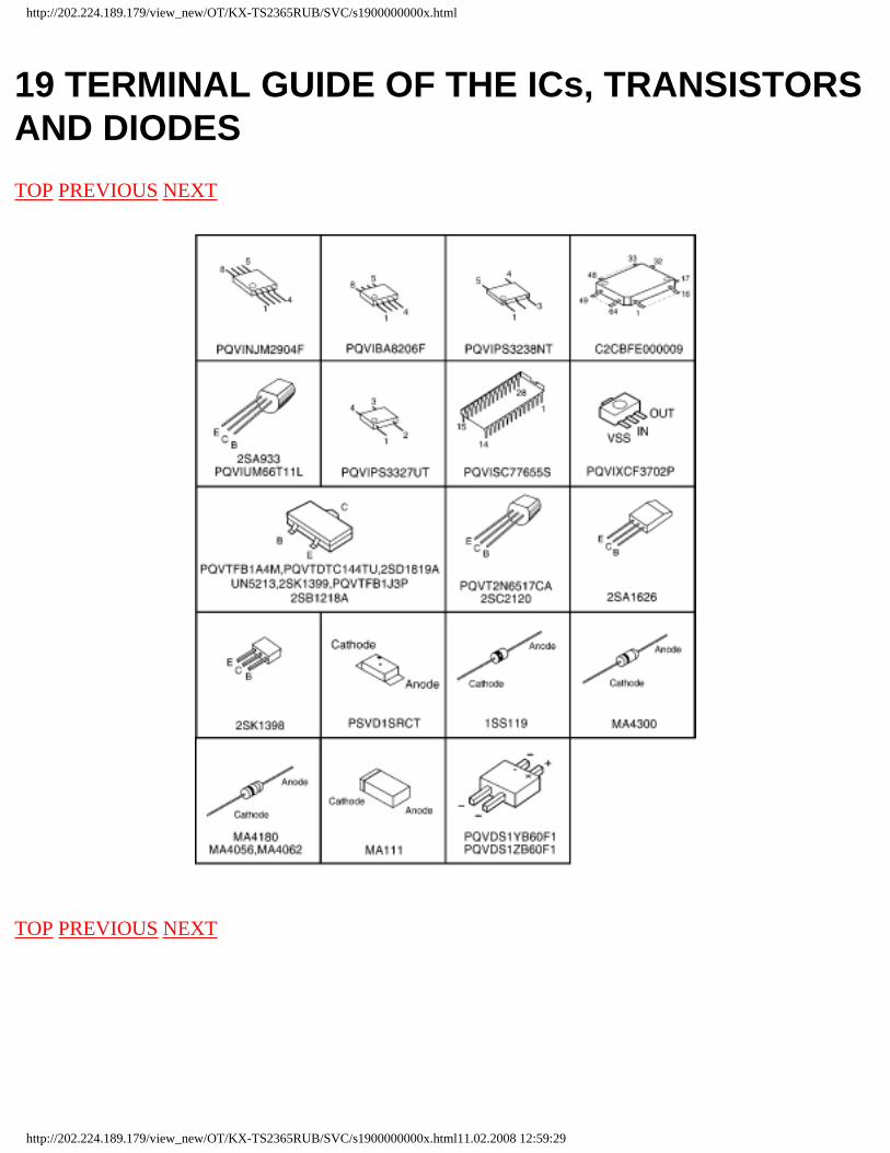
19 TERMINAL GUIDE OF THE ICs, TRANSISTORS AND DIODES
TOP PREVIOUS NEXT
TOP PREVIOUS NEXT
http://202.224.189.179/view_new/OT/KX-TS2365RUB/SVC/s1900000000x.html11.02.2008 12:59:29
http://202.224.189.179/view_new/OT/KX-TS2365RUB/SVC/s2000000000x.html
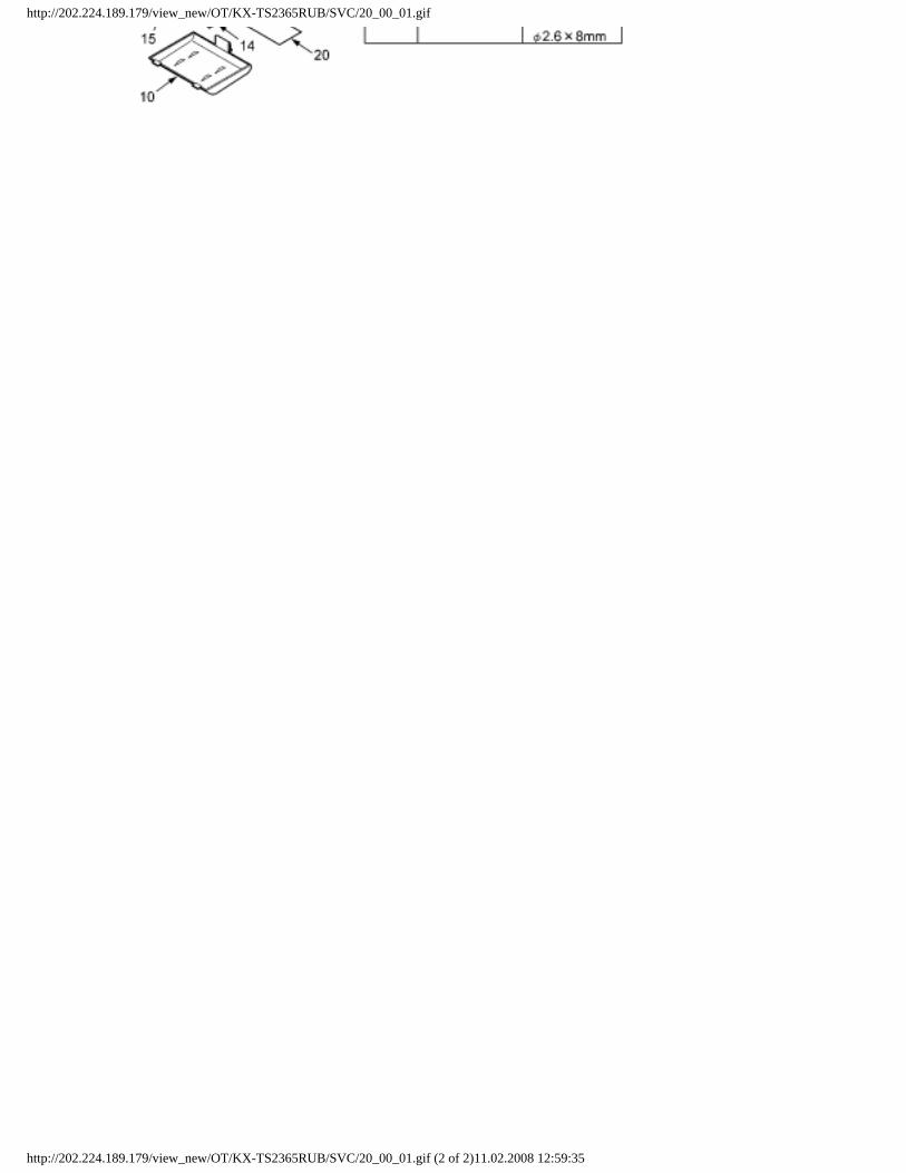
20 CABINET AND ELECTRICAL PARTS LOCATION
TOP PREVIOUS NEXT
TOP PREVIOUS NEXT
http://202.224.189.179/view_new/OT/KX-TS2365RUB/SVC/s2000000000x.html11.02.2008 12:59:33

http://202.224.189.179/view_new/OT/KX-TS2365RUB/SVC/20_00_01.gif
http://202.224.189.179/view_new/OT/KX-TS2365RUB/SVC/20_00_01.gif (1 of 2)11.02.2008 12:59:35
http://202.224.189.179/view_new/OT/KX-TS2365RUB/SVC/20_00_01.gif
http://202.224.189.179/view_new/OT/KX-TS2365RUB/SVC/20_00_01.gif (2 of 2)11.02.2008 12:59:35

http://202.224.189.179/view_new/OT/KX-TS2365RUB/SVC/s2100000000x.html
21 ACCESSORY AND PACKING MATERIALS
TOP PREVIOUS NEXT
TOP PREVIOUS NEXT
http://202.224.189.179/view_new/OT/KX-TS2365RUB/SVC/s2100000000x.html11.02.2008 12:59:44
http://202.224.189.179/view_new/OT/KX-TS2365RUB/SVC/21_00_01.gif
http://202.224.189.179/view_new/OT/KX-TS2365RUB/SVC/21_00_01.gif11.02.2008 12:59:47
http://202.224.189.179/view_new/OT/KX-TS2365RUB/SVC/s2200000000p.html
22 REPLACEMENT PARTS LIST
TOP PREVIOUS NEXT
Note:
1. RTL (Retention Time Limited)
The marking (RTL) indicates that the Retention Time is limited for this item.
After the discontinuation of this assembly in production, the item will continue to be available for a specific period of time. The retention period of availability depends on the type of assembly and the laws governing parts and product retention.
At the end of this period, the assembly will no longer be available.
2. Important safety notice
Components identified by the mark indicates special characteristics important for safety. When replacing any of these components, only use specified manufacture´s parts.
3. The S mark means the part is one of some identical parts. For that reason, it may be different from the installed part.
4. ISO code (Example: ABS-94HB) of the remarks column shows quality of the material and a flame resisting grade about plastics.
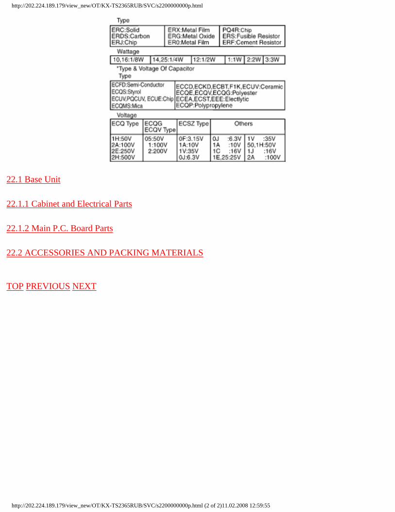
5. RESISTORS & CAPACITORS
Unless otherwise specified;
All resistors are in ohms (Ω) K=1000Ω, M=1000kΩ
All capacitors are in MICRO FARADS (μF) P=μμF
*Type & Wattage of Resistor
http://202.224.189.179/view_new/OT/KX-TS2365RUB/SVC/s2200000000p.html (1 of 2)11.02.2008 12:59:55
http://202.224.189.179/view_new/OT/KX-TS2365RUB/SVC/s2200000000p.html
22.1 Base Unit
22.1.1 Cabinet and Electrical Parts
22.1.2 Main P.C. Board Parts
22.2 ACCESSORIES AND PACKING MATERIALS
TOP PREVIOUS NEXT
http://202.224.189.179/view_new/OT/KX-TS2365RUB/SVC/s2200000000p.html (2 of 2)11.02.2008 12:59:55
http://202.224.189.179/view_new/OT/KX-TS2365RUB/SVC/s2201000000.html
22.1 Base Unit
TOP PREVIOUS NEXT
22.1.1 Cabinet and Electrical Parts
22.1.2 Main P.C. Board Parts
TOP PREVIOUS NEXT
http://202.224.189.179/view_new/OT/KX-TS2365RUB/SVC/s2201000000.html11.02.2008 13:00:01

http://202.224.189.179/view_new/OT/KX-TS2365RUB/SVC/s2201010000.html
22.1.1 Cabinet and Electrical Parts
TOP PREVIOUS NEXT
Ref. No. Part No. Part Name & Description Remarks
1 PQKM10503K2 CABINET BODY ABS-HB
2 PQYF10525S2 CABINET COVER PS-HB
3 PQBC10347Z3 BUTTON, SP PHONE ABS-HB
4 PQBH10034Z2 BUTTON, HOOK ABS-HB
5 PQBX10348Z2 BUTTON, 20KEY ABS-HB
6 PQAS57P03Z SPEAKER
7 PQGD10162Z SHEET, TEL CARD
8 PQGV10039Z TRANSPARENT PLATE, TEL CARD PC-HB
9 PQHR10875Z OPTIC CONDUCTIVE PARTS, LED LENS
PS-HB
10 PQKK10105Y2 LID, BATTERY ABS-HB
11 PQKE10070Z1 HANGER, HANDSET ABS-HB
12 PQJC10044Z BATTERY TERMINAL, (+)
13 PQJC10045Z BATTERY TERMINAL, (-)
14 PQJC313Y BATTERY TERMINAL, (+)(-)
15 PQJC314Y BATTERY TERMINAL, (-)(+)
16 PQQT22344Z LABEL, CAUTION
17 PQSX10186Y KEYBOARD SWITCH, 20KEY
18 PQSX10187Z KEYBOARD SWITCH, 6KEY
19 PQGP10190Z1 PANEL, LCD PC-HB
20 PQGT16024Z NAME PLATE
21 PQMG10025Z RUBBER PARTS, MIC COVER
TOP PREVIOUS NEXT
http://202.224.189.179/view_new/OT/KX-TS2365RUB/SVC/s2201010000.html11.02.2008 13:00:04
http://202.224.189.179/view_new/OT/KX-TS2365RUB/SVC/s2201020000.html
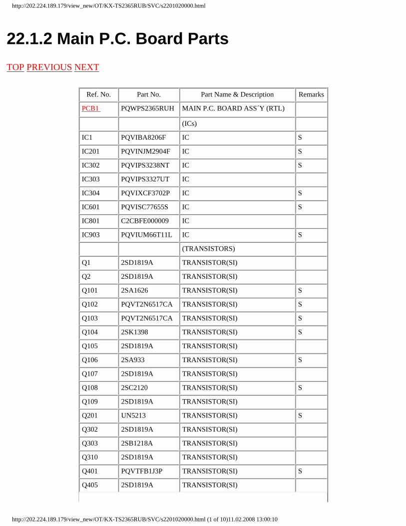
22.1.2 Main P.C. Board Parts
TOP PREVIOUS NEXT
Ref. No. Part No. Part Name & Description Remarks
PCB1 PQWPS2365RUH MAIN P.C. BOARD ASS´Y (RTL)
(ICs)
IC1 PQVIBA8206F IC S
IC201 PQVINJM2904F IC S
IC302 PQVIPS3238NT IC S
IC303 PQVIPS3327UT IC
IC304 PQVIXCF3702P IC S
IC601 PQVISC77655S IC S
IC801 C2CBFE000009 IC
IC903 PQVIUM66T11L IC S
(TRANSISTORS)
Q1 2SD1819A TRANSISTOR(SI)
Q2 2SD1819A TRANSISTOR(SI)
Q101 2SA1626 TRANSISTOR(SI) S
Q102 PQVT2N6517CA TRANSISTOR(SI) S
Q103 PQVT2N6517CA TRANSISTOR(SI) S
Q104 2SK1398 TRANSISTOR(SI) S
Q105 2SD1819A TRANSISTOR(SI)
Q106 2SA933 TRANSISTOR(SI) S
Q107 2SD1819A TRANSISTOR(SI)
Q108 2SC2120 TRANSISTOR(SI) S
Q109 2SD1819A TRANSISTOR(SI)
Q201 UN5213 TRANSISTOR(SI) S
Q302 2SD1819A TRANSISTOR(SI)
Q303 2SB1218A TRANSISTOR(SI)
Q310 2SD1819A TRANSISTOR(SI)
Q401 PQVTFB1J3P TRANSISTOR(SI) S
Q405 2SD1819A TRANSISTOR(SI)
http://202.224.189.179/view_new/OT/KX-TS2365RUB/SVC/s2201020000.html (1 of 10)11.02.2008 13:00:10
http://202.224.189.179/view_new/OT/KX-TS2365RUB/SVC/s2201020000.html
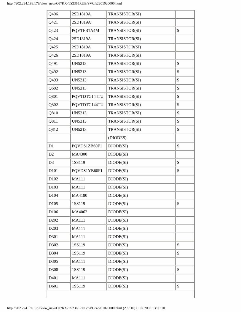
Q406 2SD1819A TRANSISTOR(SI)
Q421 2SD1819A TRANSISTOR(SI)
Q423 PQVTFB1A4M TRANSISTOR(SI) S
Q424 2SD1819A TRANSISTOR(SI)
Q425 2SD1819A TRANSISTOR(SI)
Q426 2SD1819A TRANSISTOR(SI)
Q491 UN5213 TRANSISTOR(SI) S
Q492 UN5213 TRANSISTOR(SI) S
Q493 UN5213 TRANSISTOR(SI) S
Q602 UN5213 TRANSISTOR(SI) S
Q801 PQVTDTC144TU TRANSISTOR(SI) S
Q802 PQVTDTC144TU TRANSISTOR(SI) S
Q810 UN5213 TRANSISTOR(SI) S
Q811 UN5213 TRANSISTOR(SI) S
Q812 UN5213 TRANSISTOR(SI) S
(DIODES)
D1 PQVDS1ZB60F1 DIODE(SI) S
D2 MA4300 DIODE(SI)
D3 1SS119 DIODE(SI) S
D101 PQVDS1YB60F1 DIODE(SI) S
D102 MA111 DIODE(SI)
D103 MA111 DIODE(SI)
D104 MA4180 DIODE(SI)
D105 1SS119 DIODE(SI) S
D106 MA4062 DIODE(SI)
D202 MA111 DIODE(SI)
D203 MA111 DIODE(SI)
D301 MA111 DIODE(SI)
D302 1SS119 DIODE(SI) S
D304 1SS119 DIODE(SI) S
D305 MA111 DIODE(SI)
D308 1SS119 DIODE(SI) S
D401 MA111 DIODE(SI)
D601 1SS119 DIODE(SI) S
http://202.224.189.179/view_new/OT/KX-TS2365RUB/SVC/s2201020000.html (2 of 10)11.02.2008 13:00:10
http://202.224.189.179/view_new/OT/KX-TS2365RUB/SVC/s2201020000.html
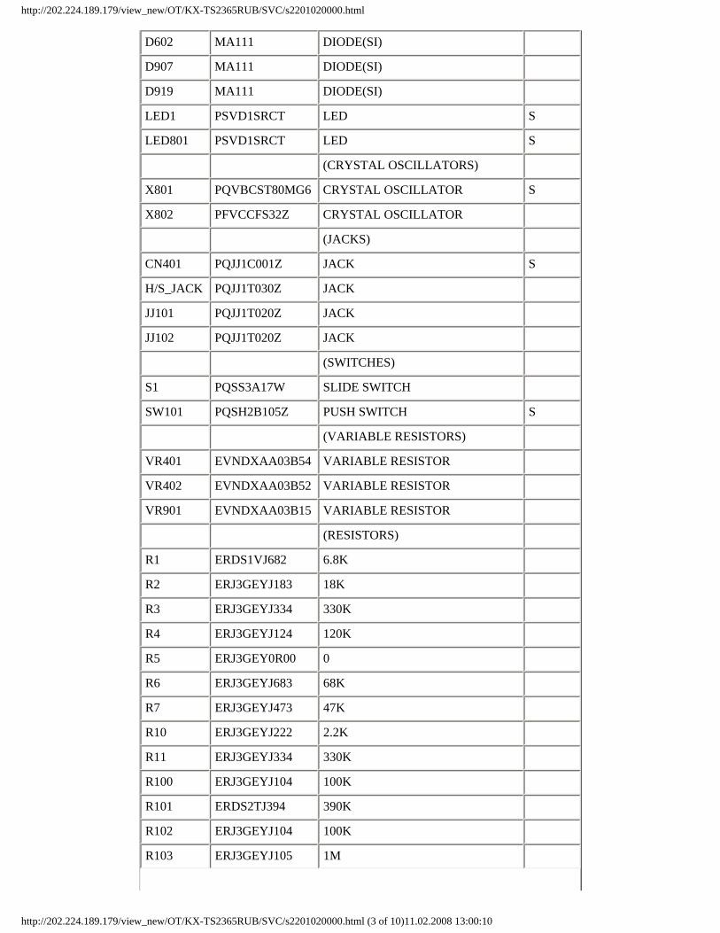
D602 MA111 DIODE(SI)
D907 MA111 DIODE(SI)
D919 MA111 DIODE(SI)
LED1 PSVD1SRCT LED S
LED801 PSVD1SRCT LED S
(CRYSTAL OSCILLATORS)
X801 PQVBCST80MG6 CRYSTAL OSCILLATOR S
X802 PFVCCFS32Z CRYSTAL OSCILLATOR
(JACKS)
CN401 PQJJ1C001Z JACK S
H/S_JACK PQJJ1T030Z JACK
JJ101 PQJJ1T020Z JACK
JJ102 PQJJ1T020Z JACK
(SWITCHES)
S1 PQSS3A17W SLIDE SWITCH
SW101 PQSH2B105Z PUSH SWITCH S
(VARIABLE RESISTORS)
VR401 EVNDXAA03B54 VARIABLE RESISTOR
VR402 EVNDXAA03B52 VARIABLE RESISTOR
VR901 EVNDXAA03B15 VARIABLE RESISTOR
(RESISTORS)
R1 ERDS1VJ682 6.8K
R2 ERJ3GEYJ183 18K
R3 ERJ3GEYJ334 330K
R4 ERJ3GEYJ124 120K
R5 ERJ3GEY0R00 0
R6 ERJ3GEYJ683 68K
R7 ERJ3GEYJ473 47K
R10 ERJ3GEYJ222 2.2K
R11 ERJ3GEYJ334 330K
R100 ERJ3GEYJ104 100K
R101 ERDS2TJ394 390K
R102 ERJ3GEYJ104 100K
R103 ERJ3GEYJ105 1M
http://202.224.189.179/view_new/OT/KX-TS2365RUB/SVC/s2201020000.html (3 of 10)11.02.2008 13:00:10

http://202.224.189.179/view_new/OT/KX-TS2365RUB/SVC/s2201020000.html
R104 ERJ3GEYJ473 47K
R105 ERJ3GEYJ684 680K
R107 ERJ3GEYJ394 390K
R108 ERDS2TJ332 3.3K
R109 ERJ3GEYJ182 1.8K
R110 ERJ3GEYJ104 100K
R111 ERJ3GEYJ103 10K
R115 ERJ3GEY0R00 0
R116 ERJ3GEYJ473 47K
R117 ERJ3GEYJ682 6.8K
R118 ERJ3GEYJ103 10K
R119 ERJ3GEYJ104 100K
R120 ERJ3GEYJ152 1.5K
R121 ERJ3GEYJ103 10K
R123 ERJ3GEYJ560 56
R124 ERDS1TJ150 15 S
R125 ERJ3GEYJ103 10K
R126 ERJ3GEYJ335 3.3M
R127 ERJ3GEYJ472 4.7K
R128 ERJ3GEYJ470 47
R129 ERJ3GEYJ334 330K
R130 ERJ3GEYJ272 2.7K
R131 ERJ3GEYJ332 3.3K
R184 ERJ3GEY0R00 0
R185 ERJ3GEY0R00 0
R201 ERDS2TJ103 10K
R202 ERJ3GEYJ124 120K
R203 ERJ3GEYJ103 10K
R204 ERJ3GEYJ394 390K
R205 ERJ3GEYJ562 5.6K
R206 ERJ3GEYJ183 18K
R207 ERJ3GEYJ103 10K
R208 ERJ3GEYJ472 4.7K
R209 ERJ3GEYJ104 100K
http://202.224.189.179/view_new/OT/KX-TS2365RUB/SVC/s2201020000.html (4 of 10)11.02.2008 13:00:10

http://202.224.189.179/view_new/OT/KX-TS2365RUB/SVC/s2201020000.html
R211 ERJ3GEYJ473 47K
R301 ERJ3GEYJ225 2.2M
R302 ERJ3GEYJ685 6.8M
R303 ERJ3GEYJ225 2.2M
R304 ERJ3GEYJ475 4.7M
R305 ERJ3GEYJ221 220
R310 ERJ3GEYJ223 22K
R311 ERJ3GEYJ104 100K
R312 ERJ3GEYJ104 100K
R313 ERJ3GEYJ104 100K
R315 ERJ3GEY0R00 0
R316 ERJ3GEY0R00 0
R320 ERJ3GEYJ103 10K
R321 ERJ3GEYJ101 100
R322 ERJ3GEYJ473 47K
R323 ERJ3GEYJ103 10K
R401 ERJ3GEYJ333 33K
R403 ERJ3GEYJ473 47K
R404 ERJ3GEYJ183 18K
R405 ERJ3GEYJ473 47K
R406 ERJ3GEYJ225 2.2M
R407 ERJ3GEYJ222 2.2K
R408 ERJ3GEYJ681 680
R409 ERJ3GEYJ223 22K
R410 ERJ3GEYJ564 560K
R411 ERJ3GEYJ681 680
R412 ERJ3GEYJ822 8.2K
R421 ERJ3GEYJ272 2.7K
R423 ERJ3GEY0R00 0
R424 ERJ3GEYJ334 330K
R425 ERJ3GEYJ225 2.2M
R426 ERJ3GEYJ272 2.7K
R427 ERJ3GEYJ121 120
R428 ERJ3GEYJ562 5.6K
http://202.224.189.179/view_new/OT/KX-TS2365RUB/SVC/s2201020000.html (5 of 10)11.02.2008 13:00:10
http://202.224.189.179/view_new/OT/KX-TS2365RUB/SVC/s2201020000.html
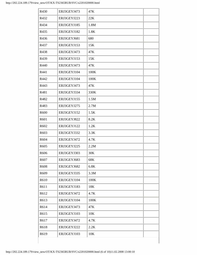
R430 ERJ3GEYJ473 47K
R432 ERJ3GEYJ223 22K
R434 ERJ3GEYJ185 1.8M
R435 ERJ3GEYJ182 1.8K
R436 ERJ3GEYJ681 680
R437 ERJ3GEYJ153 15K
R438 ERJ3GEYJ473 47K
R439 ERJ3GEYJ153 15K
R440 ERJ3GEYJ473 47K
R441 ERJ3GEYJ104 100K
R442 ERJ3GEYJ104 100K
R443 ERJ3GEYJ473 47K
R481 ERJ3GEYJ334 330K
R482 ERJ3GEYJ155 1.5M
R483 ERJ3GEYJ275 2.7M
R600 ERJ3GEYJ152 1.5K
R601 ERJ3GEYJ822 8.2K
R602 ERJ3GEYJ122 1.2K
R603 ERJ3GEYJ332 3.3K
R604 ERJ3GEYJ472 4.7K
R605 ERJ3GEYJ225 2.2M
R606 ERJ3GEYJ303 30K
R607 ERJ3GEYJ683 68K
R608 ERJ3GEYJ682 6.8K
R609 ERJ3GEYJ335 3.3M
R610 ERJ3GEYJ104 100K
R611 ERJ3GEYJ183 18K
R612 ERJ3GEYJ472 4.7K
R613 ERJ3GEYJ104 100K
R614 ERJ3GEYJ473 47K
R615 ERJ3GEYJ103 10K
R617 ERJ3GEYJ472 4.7K
R618 ERJ3GEYJ222 2.2K
R619 ERJ3GEYJ103 10K
http://202.224.189.179/view_new/OT/KX-TS2365RUB/SVC/s2201020000.html (6 of 10)11.02.2008 13:00:10
http://202.224.189.179/view_new/OT/KX-TS2365RUB/SVC/s2201020000.html
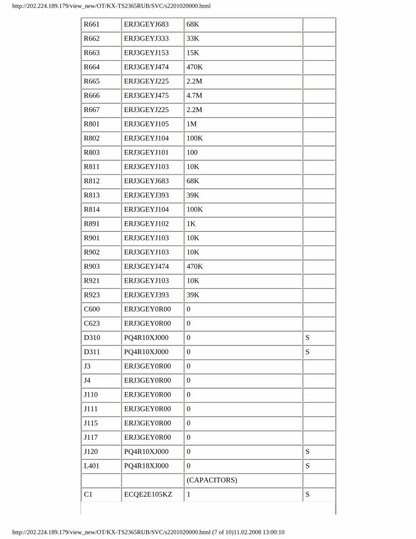
R661 ERJ3GEYJ683 68K
R662 ERJ3GEYJ333 33K
R663 ERJ3GEYJ153 15K
R664 ERJ3GEYJ474 470K
R665 ERJ3GEYJ225 2.2M
R666 ERJ3GEYJ475 4.7M
R667 ERJ3GEYJ225 2.2M
R801 ERJ3GEYJ105 1M
R802 ERJ3GEYJ104 100K
R803 ERJ3GEYJ101 100
R811 ERJ3GEYJ103 10K
R812 ERJ3GEYJ683 68K
R813 ERJ3GEYJ393 39K
R814 ERJ3GEYJ104 100K
R891 ERJ3GEYJ102 1K
R901 ERJ3GEYJ103 10K
R902 ERJ3GEYJ103 10K
R903 ERJ3GEYJ474 470K
R921 ERJ3GEYJ103 10K
R923 ERJ3GEYJ393 39K
C600 ERJ3GEY0R00 0
C623 ERJ3GEY0R00 0
D310 PQ4R10XJ000 0 S
D311 PQ4R10XJ000 0 S
J3 ERJ3GEY0R00 0
J4 ERJ3GEY0R00 0
J110 ERJ3GEY0R00 0
J111 ERJ3GEY0R00 0
J115 ERJ3GEY0R00 0
J117 ERJ3GEY0R00 0
J120 PQ4R10XJ000 0 S
L401 PQ4R18XJ000 0 S
(CAPACITORS)
C1 ECQE2E105KZ 1 S
http://202.224.189.179/view_new/OT/KX-TS2365RUB/SVC/s2201020000.html (7 of 10)11.02.2008 13:00:10

http://202.224.189.179/view_new/OT/KX-TS2365RUB/SVC/s2201020000.html
C2 ECEA1HU100 10
C3 ECEA1HUR22 0.22
C5 ECUV1H822KBV 0.0082
C6 ECEA1HKA010 1
C8 ECUV1C104KBV 0.1
C100 ECUV1C104KBV 0.1
C101 ECKD2H681KB 680P S
C102 ECKD2H681KB 680P S
C103 ECUV1H103KBV 0.01
C105 ECEA1CU221 220
C106 ECEA1HU100 10 S
C107 ECEA1AU331 330
C108 ECUV1C104KBV 0.1
C109 ECUV1H103KBV 0.01
C111 ECUV1H103KBV 0.01
C112 ECUV1C104KBV 0.1
C113 ECUV1H183KBV 0.018
C114 ECEA1AU470 47
C201 ECUV1C473KBV 0.047
C202 ECEA1EU470 47 S
C203 ECUV1H222KBV 0.0022
C204 ECUV1C473KBV 0.047
C205 PQCUV1C224KB 0.22
C301 ECA0JM471 470P
C302 ECEA0JKA331 330
C303 ECEA0JU331 330
C304 PQCUV1H333JC 0.033 S
C306 ECUV1C104ZFV 0.1
C308 ECEA0JKA221 220
C310 ECEA1CKS470 47 S
C404 ECUV1C104KBV 0.1
C405 ECUV1C104KBV 0.1
C408 ECUV1H472KBV 0.0047
C414 ECEA1CKA100 10
http://202.224.189.179/view_new/OT/KX-TS2365RUB/SVC/s2201020000.html (8 of 10)11.02.2008 13:00:10

http://202.224.189.179/view_new/OT/KX-TS2365RUB/SVC/s2201020000.html
C415 ECUV1H103KBV 0.01
C421 ECUV1H103KBV 0.01
C422 ECUV1E223KBV 0.022
C423 ECUV1H103KBV 0.01
C424 ECUV1H682KBV 0.0068
C425 ECUV1C104KBV 0.1
C426 ECUV1C104KBV 0.1
C435 ECUV1C104KBV 0.1
C438 ECUV1C104KBV 0.1
C481 ECUV1H103KBV 0.01
C601 ECA0JM102B 0.001
C602 ECUV1C473KBV 0.047
C603 ECUV1H333KBV 0.033 S
C605 ECUV1E223KBV 0.022
C606 ECUV1C683KBV 0.068
C607 ECUV1C273KBV 0.027
C608 ECUV1H153KBV 0.015
C609 ECUV1C104KBV 0.1
C610 ECEA1HKA010 1
C611 ECEA1HKA010 1
C612 ECEA1VKS4R7 4.7 S
C613 ECUV1C683KBV 0.068
C614 ECEA1EU470 47 S
C615 ECEA0JU220 22
C616 ECUV1C104KBV 0.1
C617 ECEA1CKS470 47 S
C618 ECEA1VU330 33 S
C619 ECEA1VKS4R7 4.7 S
C620 ECUV1H183KBV 0.018
C621 ECEA0JKA101 100
C622 ECUV1C104KBV 0.1
C624 ECUV1H103KBV 0.01
C625 ECEA1AU101 100
C801 ECUV1H103KBV 0.01
http://202.224.189.179/view_new/OT/KX-TS2365RUB/SVC/s2201020000.html (9 of 10)11.02.2008 13:00:10
http://202.224.189.179/view_new/OT/KX-TS2365RUB/SVC/s2201020000.html
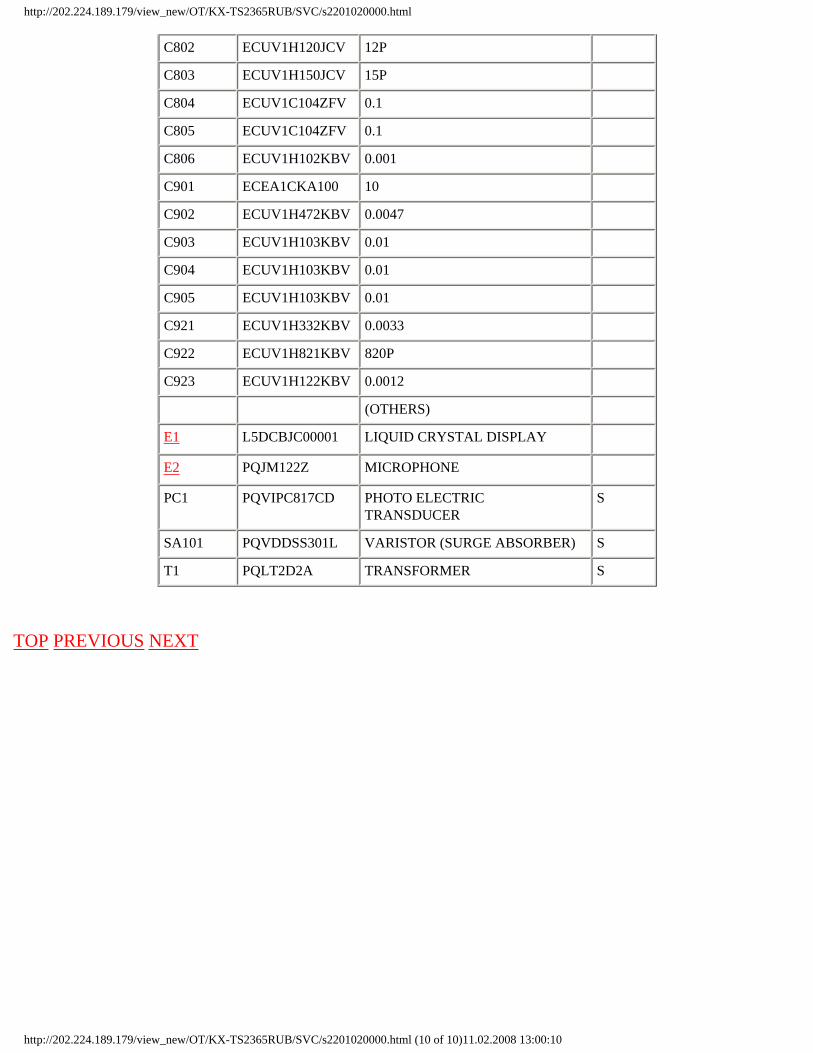
C802 ECUV1H120JCV 12P
C803 ECUV1H150JCV 15P
C804 ECUV1C104ZFV 0.1
C805 ECUV1C104ZFV 0.1
C806 ECUV1H102KBV 0.001
C901 ECEA1CKA100 10
C902 ECUV1H472KBV 0.0047
C903 ECUV1H103KBV 0.01
C904 ECUV1H103KBV 0.01
C905 ECUV1H103KBV 0.01
C921 ECUV1H332KBV 0.0033
C922 ECUV1H821KBV 820P
C923 ECUV1H122KBV 0.0012
(OTHERS)
E1 L5DCBJC00001 LIQUID CRYSTAL DISPLAY
E2 PQJM122Z MICROPHONE
PC1 PQVIPC817CD PHOTO ELECTRIC TRANSDUCER
S
SA101 PQVDDSS301L VARISTOR (SURGE ABSORBER) S
T1 PQLT2D2A TRANSFORMER S
TOP PREVIOUS NEXT
http://202.224.189.179/view_new/OT/KX-TS2365RUB/SVC/s2201020000.html (10 of 10)11.02.2008 13:00:10
http://202.224.189.179/view_new/OT/KX-TS2365RUB/SVC/s2202000000.html
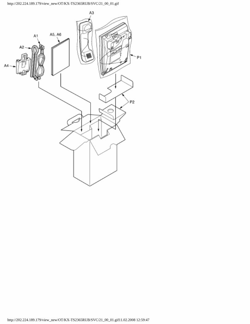
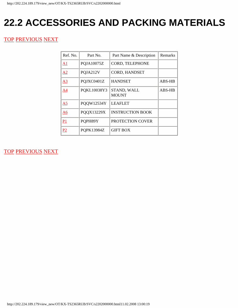
22.2 ACCESSORIES AND PACKING MATERIALS
TOP PREVIOUS NEXT
Ref. No. Part No. Part Name & Description Remarks
A1 PQJA10075Z CORD, TELEPHONE
A2 PQJA212V CORD, HANDSET
A3 PQJXC0401Z HANDSET ABS-HB
A4 PQKL10038Y3 STAND, WALL MOUNT
ABS-HB
A5 PQQW12534Y LEAFLET
A6 PQQX13229X INSTRUCTION BOOK
P1 PQPH89Y PROTECTION COVER
P2 PQPK13984Z GIFT BOX
TOP PREVIOUS NEXT
http://202.224.189.179/view_new/OT/KX-TS2365RUB/SVC/s2202000000.html11.02.2008 13:00:19
http://202.224.189.179/view_new/OT/KX-TS2365RUB/SVC/s2300000000x.html
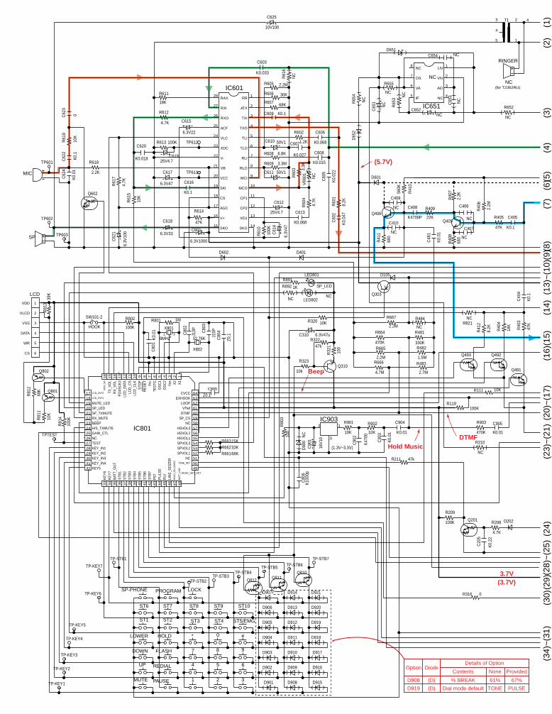
23 FOR SCHEMATIC DIAGRAM ( SCHEMATIC DIAGRAM )
TOP PREVIOUS NEXT
1. DC voltage measurements are taken with electronic voltmeter from negative terminal.
(Add 40 mA to telephone line from the loop simulator.)
2. This schematic diagram may be modified at any time with the development of new technology.
Important Safety Notice: Components identified by mark have special characteristics important for safety. When replacing any of these components, use
only the manufacturer´sspecified parts.
TOP PREVIOUS NEXT
http://202.224.189.179/view_new/OT/KX-TS2365RUB/SVC/s2300000000x.html11.02.2008 13:00:23
http://202.224.189.179/view_new/OT/KX-TS2365RUB/SVC/s2400000000x.html
24 SCHEMATIC DIAGRAM
TOP PREVIOUS NEXT
TOP PREVIOUS NEXT
http://202.224.189.179/view_new/OT/KX-TS2365RUB/SVC/s2400000000x.html11.02.2008 13:00:40
DTMFHold Music
Beep
(5.7V)
3.7V(3.7V)
Option DiodeContents
Details of Option
None Provided
D908 (D) % BREAK 61% 67%
D919 (D) Dial mode default TONE PULSE
C60
2
K0.
047
ST8
ST4
R607 68K
SP
C61
4
6.3V
47
C48
1
K0.
01
C80
3
J15P
Q602
Z0.1
C805
7
3
R611
18K
R608 6.8K
C62
2
K0.
1
ST10
R618
2.2K
R605 2.2M
R666
4.7M
C80
2
J12P
R483
2.7M
1RR
2ATX
3TXI
4TXO
5TLI
6TLO
7RLI
8RLO
9MCI
10MCO
11CP1
12CP2
13XD1
14SKG
15SKO
16V+
17AGC
18CS
19SKI
20VCC
21VB
22V-
23XDC
24VLC
25ACF
26RXO
27RXI
28RAX
R613 100K
8
D906
C607
K0.027
X801
8MHz1
23
R60
1
8.2K
C609 K0.1
C615
6.3V22
R665
2.2M
R208
4.7K
R209
100K
D902
R614
47K
R61
0
100K
C617
6.3V47R61
7
4.7K
1
9
R482
1.5M
D904
C618
6.3V33
R606 30K
Q201
C610 50V1
#
2
C616
K0.1
C60
5
K0.
022
MIC
ST5/EMG
R609 3.3M
C613
K0.068
R602
1.2K
LOCK
X802
32.76K
5
4
C620
K0.018
R61
5
10K
R612
4.7K
1MR801
C611 50V1
C612
25V4.7
C62
4
K0.
01
0
K0.
01C
801
C608
K0.015
4
C61925V4.7
C62
1
6.3V
100
*
6
ST9
D903
NC
1LN
2VN
3AD
4NC
5IF
6VA
7OS
8NC
D909
D914
D908
D911
D912
D913
D910
D918
D916
D921
D920
D915
D917
ST6
LOWER
MUTE
UP
SP-PHONE
DOWN
PAUSE
ST7
REDIAL
PROGRAM
FLASH
HOLD
ST1 ST2 ST3
Q406
R40
8
680
R41
1
680
R40
7
2.2K
Q405
R409
22K
C408
K4700P
68KR66133KR66215KR663
R40
4
18K
R40
3
47K
C90
1
16V
10
R902
10K
C90
3
K0.
01
R901
10K
C904
K0.01
C90
2
K47
00
(1.3V~3.3V)
1
3
2
R664
470K
R481
330K
C905
K0.01
R903
470K
T13
4
5 1
2
C405
K0.1
R405
47K
C40
4
K0.
1
C625
10V100
RINGER
NC(for T2362RU)
C606
K0.068R61
9
10K
VR
601
NCR60
3 3.3K
C62
3
0
R60
4
4.7K
C601
6.3V1000
C80
4
Z0.1
R655
NC
R65
3 NC
C65
1
NC
C652NC
C65
3
NC
C654 NCD651
D65
2R
654
NC
D601
LCD
1VDD
2VLCD
3VSS
4DATA
5WR
6CS
LED801
SP_LED
R210
NC
D202
C410
NCC407
NC
R41
2
8.2K
C603
K0.033
R119100K
100
R80
3
D90
0N
CC
806
K10
00p
R652
NC
R40
6
2.2M
39K
R81
3
R891
1K
100K
R802
HOOK
SW101-2R821
NC
1X
12
X2
3V
ss4
OS
C2
5O
SC
16
TES
TG7
Vcc
8R
ES
ET
9S
TOP
10
LCD
_CLK
11
LCD
_CS
12
LCD
_DAT
A1
3P
24/S
CK
31
4R
X_V
OL
15
TX_V
OL
16
HOO
K_SW
17 LCD_CNT2
18 LCD_CNT1
19 MUTE_LED20 SP_LED21 SP_TXMUTE22 RX_MUTE23 BEEP24 H/S_TXMUTE25 GAIN_CTL26 NC27 TEST28 KEY_IN129 KEY_IN230 KEY_IN331 KEY_IN432 KEY5
33
KE
Y6
34
KE
Y7
35
BAT
T_O
UT
36
STB
13
7S
TB2
38
STB
33
9S
TB4
40
STB
54
1S
TB6
42
STB
74
3P
674
4P
ULS
E4
5R
LY4
6LI
NE
_SE
IZE
R4
7H
OLD
_ON
_MU
SIC
48
BAT
T_LO
W 49HEAD_SET_DET
50TONE_DET
51NC52SPVOL153SPVOL254SPVOL355HSVOL156HSVOL257HSVOL358NC59SP_CS60DTMF61VTref62LOOP63EXHOOK64CVCC
D602 D401
TP601
TP603
TP602
TP611
TP612
TP-KEY1
TP-KEY2
TP-KEY3
TP-KEY4
TP-KEY5
TP-KEY6
TP-KEY7
TP-STB1
TP-STB2TP-STB3
TP-STB4TP-STB5 TP-STB6
TP-STB7
C20
5
K0.
22
R61
6
NC
Q493 Q492
Q491
68K
R81
2
10K
R81
1
TPTEST
100K
R81
4
R667
2.2M
D105
Q801
Q802
Q303
R320 10K
D907
R892
NC LED802NC
R484
NC
NC
C409
R41
0
560K
R111 10K
D919D905
D901
C406
NC
R32247k
R323
10k
R32
1
100
C310 6.3V47u
R211 47k
R316 0
Q310
Q810Q811Q812
(30)
(29)
(23)
~(2
1)(2
0)~
(17)
(13)
~(1
0)(2
4)(1
6)(1
5)(1
4)(7
)(4
)(5
)(6
)(8
)(9
)(3
)(2
)(1
)(2
8)~
(25)
(34)
~(3
1)
IC651
IC601
IC801IC903
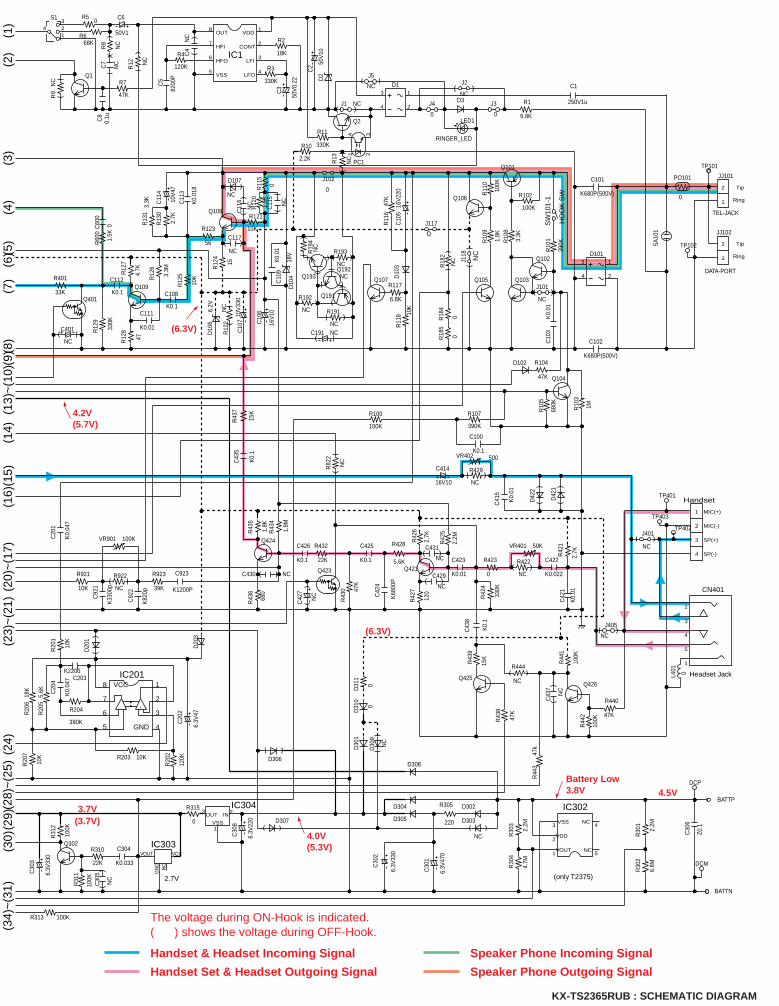
Speaker Phone Outgoing Signal
Speaker Phone Incoming SignalHandset & Headset Incoming Signal
Handset Set & Headset Outgoing Signal
The voltage during ON-Hook is indicated.( ) shows the voltage during OFF-Hook.
KX-TS2365RUB : SCHEMATIC DIAGRAM
Battery Low 3.8V
4.0V(5.3V)
4.2V (5.7V)
4.5V
(6.3V)
3.7V(3.7V)
(6.3V)
R42
6
2.7K
C3
50V
0.22
D10
418
V
R20
2
120K
R10
3
1M
BATTN
C426
K0.1
C11
3
K0.
018
C923
K1200P
R12
5
10K
R20
7
10K
C10
516
V22
0
R923
39K
R10
8
3.3K
R43
7
15K
R204
390K
R20
1
10K
JJ101
TEL-JACK
Ring1
Tip2
R12
0
1.5K
1VDD
2CONT
3LFI
4LFO
5VSS
6HFO
7HFI
8OUT
C20
4
K0.
047
C5
8200
P
D302
R43
5
1.8K
C41
5
K0.
01
R20
618
K
R10
5
680K
R305
220
R43
6
680
R123
56
R104
47K
C1
250V1u
R42
7
120
D10
3
C10
6
16V
10
Q108
R4
120K R3
330K
R117
6.8K
R203 10K
R42
5
2.2M
R11
647
K
C30
1
6.3V
470
C92
2
K82
0p
R12
9
330K
+ -- +
1
2
3
GND 45
6
7
8 VCC
C423
K0.01
R102
100K
C203K2200
Q109
Q101
Q421
Q107
R12
7
4.7K
Q424
R12
8
47
R1
6.8K
D10
66.
2V
D304
C108
K0.1C
2 50V
10
R43
4
1.8M
C20
2
6.3V
47
C10
710
V33
0
C20
1
K0.
047
R121
10K
C111
K0.01D
2
C10
3K
0.01
S1
4123
R12
4
15C
435
K0.
1
Q104
D305
R50
R921
10K
R10
1
390K
R20
55.
6KR2
18K
Q423
BATTP
R432
22K
C425
K0.1
C92
1
K33
00p
R11
8 10K
C112
K0.1
D102
Q103
R43
0 47K
C30
3
6.3V
330
Q302
R31
2
100K
JJ102
DATA-PORT
Ring1
Tip2
D1
4
3 1
2
C102
K680P(500V)
C101
K680P(500V)
PO101
0
SA
101
J102
0
R19
4N
C
R193
NC
R192
NC R191
NC
Q193
Q191
C191 NC
R401
33K
C6
50V1
C4
NCR6
68K
Q1R7
47K
C422
K0.022
C42
1
K0.
01
R423
0
R42
1
2.7K
R428
5.6K
J405
NC
R43
9
15K
R44
2
100K
R44
1
100K
Q426
CN401
Headset Jack
1
5
4
3
2
R440
47K
Q425
J401
NC
R43
8
47K
R9
NC
C43
8
K0.
1
C11
4
10V
47
R13
0
2.7K
C30
6
Z0.1
R30
1
2.2M
R30
3
2.2M
R30
2
6.8M
(only T2375)
1VOUT
2VDD
3VSS
4NC
5NC
R30
4
4.7M
D306
D307
D20
3
Handset
1 MIC(+)
2 MIC(-)
3 SP(+)
4 SP(-)
D20
1
C414
16V10
D42
1
D42
2
R12
2N
C
C10
9K
0.01
R82
2
NC
R18
2
NC
R60
0
1.5K
C60
0
0
C11
5
NC
22K
R310
K0.033
C304
2.7V
VCCVOUT
NC
GN
D
100K
R31
1
D308
R12
6
3.3M
SW
101-
1
HO
OK
SW
NC
C30
5
R444
NC
PC1
1 234
C117
NC
C401
NC
3OUT
1VSS
2IN
NC
C43
7
C42
7
NC
C429
NC
C430 NC
D31
0
0
DCP
DCM
TP101
TP102
TP401
TP403
TP402
R313 100K
NCQ192
C431
NC
C30
8
6.3V
220
R107
390K
J118
NC
R18
4
0
D107
NC
C11
6
NC
D303
NC
D30
9
NC
L401 0
C42
4
K68
00P
C30
2
6.3V
330
J1 NC
Q2
R10
2.2K
R11
330K
J101
NC
Q102
R10
9
1.8K
Q106
J117
0
R429
NC
VR402 500
VR401 50K
R422
NC
R11
0
100K
R42
4
330K
D101
4
3 1
2
Q401
Q105
J3
0
NC
J2
D3
J5
NC
R12 N
C
LED1
RINGER_LED
J4
0
R13
NC
NCC7
NC
R8
R922
NC
VR901 100K
D31
1
0
R13
13.
3K
R44
347
kD30
1
C8
0.1u
C100
K0.1
R100
100K
0
R315
R18
5
0
R11
5
0
(30)
(29)
(23)
~(2
1)(2
0)~
(17)
(13)
~(1
0)(2
4)(1
6)(1
5)(1
4)(7
)(4
)(5
)(6
)(8
)(9
)(3
)(2
)(1
)(2
8)~
(25)
(34)
~(3
1)
IC201
IC1
IC304 IC302
IC303
http://202.224.189.179/view_new/OT/KX-TS2365RUB/SVC/s2500000000x.html
25 CIRCUIT BOARD
TOP PREVIOUS NEXT
25.1 Component View
25.2 Flow Solder Side View
TOP PREVIOUS NEXT
http://202.224.189.179/view_new/OT/KX-TS2365RUB/SVC/s2500000000x.html11.02.2008 13:01:00

http://202.224.189.179/view_new/OT/KX-TS2365RUB/SVC/s2501000000.html
25.1 Component View
TOP PREVIOUS NEXT
TOP PREVIOUS NEXT
http://202.224.189.179/view_new/OT/KX-TS2365RUB/SVC/s2501000000.html11.02.2008 13:01:02

IC801IC201
IC1
IC304
IC651
IC302
SP-SHONE
IC303
PR
OG
RA
M
LOC
K
CB E
CB E
CB E
CB E
CB E
CB E
CB E
CB E
CB E
CB E
CB E
CB E
E BC
E BC
E BC
E BC
E BC
E BC
E BC
E BC
E BC
C409
R412
R422
C410R
410C408
R407
C438R439
R409
R821
R404
R403
R401
C112
R438C423
C429
C431
C405R405R408
R411
C404
R424
Q426
Q423
Q401
Q406
Q109
Q602
Q303
R437
C923R
923 C622
C922
C921
R922
R619 R
618
C905
R903
R302
R304
R303
TPS
TB2
147
23
PA
US
E
RE
DIA
L
FLA
SH
HO
LD
69#
580
TP101
D1
Q2
PC
1
TP102
C306
R301
TP601
DC
M
TP612
TP611
Q493
Q492
Q491
Q425
Q421
Q405
Q424
R427C424
R428R430
C425
R425R822
C426
C430R432
R436
D920
D921
DO
WN
D913
D914
D906
D907
D919
D918
UP
D912
D911
D905
D904
J114
C435R435
R426
R423
R434
C437
R442
R441
R421
R129 C
111R
128
C415
C108
R125
C422
C421
R126
R429
R305
C481
R600
R320 C
653C
654
R483
C600
R615
R667
R484
D306
D311
D310
D301
D309 R
664R
666
R481
R482
R653R
655
J405
J401
R665 C
608R
608
R607
R606
R130
R131
R123
C607
C117
R602
RE
DB
LAC
K
RIN
GE
R
C623 R
610
R614
C616
R617
C606C
605R
616C
603R
611
J115
R613
C620R
612R
601
R652
C113
C115
C109 R
813
R110
J110
R119
C103
C201
J3J2~ ~
+ -
R102
J120
R9
Q1
R10
C4
8 5
1 4
1 458
R2
R3
C5
R4
R13
R8
R5
R6
R7
R11
J4J5R
12
R103
R105
C204C
203J111R
104R
109
R661
R211 D
900
R662
R663
R204
R202R
208C
205
Q201
D203
R207
R203
R205
R182
R118
R117
D103
R116
Q193
Q192
R193
R120
R115
R122
R121
J117J118
R184
ST
4
ST
5/EM
G
ST
8
ST
7
ST
6
ST
9
ST
10
LOW
ER
ST
3
ST
1
ST
2
C116
L401
C602
D305
R127
R440
R444
R406C406
C407
E BC
Q823
E BCQ
821
E BC Q
822
D202
1
16
17
32 33
48
49
64
D102
LED
1
D916
D909
D903
D910D
917
LED
801LE
D802
SP
PH
ON
EM
UT
E
D401
D602
D908
D915
D902
D910
CB E
Q107
CB E
CB E
C613 R
604
R609
R605
R603
C609R
107
R921
C8
C904
R902
R901
C902
C903
C805
C802
R312
R316
C801
C806
R313
C304
C803
Q302
C804
R315
R311
R310
R801
R802
C305
R812
R811
Q802
E BC Q
811
E BC Q
812
Q801
R814
R322
R323
R321
R891
R892
R831
R206
R111
R803
Q105R
209
R186
R185
C624
J113
R100
C100
J112
R443
TPS
TB3
TPK
EY
1
TPK
EY
3
TPK
EY
4
TPK
EY
7
TPS
TB4
TPS
TB1
TPS
TB5
TPS
TB7
TPS
TB6
DC
P
SP
LED
MU
TELE
D
TPK
EY
2
TPK
EY
5
TPK
EY
6TP
TES
TCB EQ
810
CB E
Q310
SP
H/S
MIC
KX-TS2365RUB CIRCUIT BOARD (Component View)

http://202.224.189.179/view_new/OT/KX-TS2365RUB/SVC/s2502000000.html
25.2 Flow Solder Side View
TOP PREVIOUS
TOP PREVIOUS
http://202.224.189.179/view_new/OT/KX-TS2365RUB/SVC/s2502000000.html11.02.2008 13:01:11

J56
J25
J63J64
J65
X801
X802
IC903
J26
J90J91
J61 J13
J60J69J62
J81
J92J93
R B Y G
H/S
_JAC
K
C401
VR401 VR402 VR901
VR601
J66
J57
C427
D107
D651
D104 LC
D
D106
J80
J10
D652
D601
D308
D421
D304
C302
C301
C414
J32
J30
J67
J68
J54
J55
J27
J22
J94
J84
J95
J96J97
J28J29J31
MIC
D307
R210
D302
D303
D422
C625
SPC618
C621C619
C651
R654
IC601
C308
J23
J82
J21
J52
D105
D3
J19
J83
J53
J18
C105
C101C102
C901
C202
J51
J50J14
J12
SW101J24
J20
C114
R194
R201
R101
J101
JJ101JJ102
R108
R191
R1
R192 J102
Q191
J35
J1
J34C1
C3
C6
C612
C611
C303
C652
J36
J15J16
J17Q
108E
C B
Q106
D2
T1
D101
Q102
Q104 Q
103
Q101
CN
401
C614
C617
C615
1415
281
C610
C106 C
191
C107
C2
S1
PC
1
R124
C601
C310
PO
101
SA
101
ECB
E C
B
E C
BE
C B
B C
E
B C
E
KX-TS2365RUB CIRCUIT BOARD (Flow Solder Side View)
PbF