session 5: solid state physics charge mobility drift ...ee.sharif.edu/~sarvari/25772/pssd005.pdf ·...
TRANSCRIPT

Charge Mobility
Drift
Diffusion
Recombination-Generation
Session 5: Solid State Physics
1
1. Introduction
2. Crystal
3. Cubic Lattices
4. Other
5. Miller Indices
Outline
� A� B
� C
� D
� E
� F� G
� H
� I
� J
2
1. Introduction
2. Crystal
3. Cubic Lattices
4. Other
5. Miller Indices
Mobile Charge Carriers in Semiconductors
3
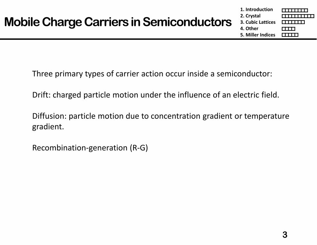
Three primary types of carrier action occur inside a semiconductor:
Drift: charged particle motion under the influence of an electric field.
Diffusion: particle motion due to concentration gradient or temperature
gradient.
Recombination-generation (R-G)
1. Introduction
2. Crystal
3. Cubic Lattices
4. Other
5. Miller Indices
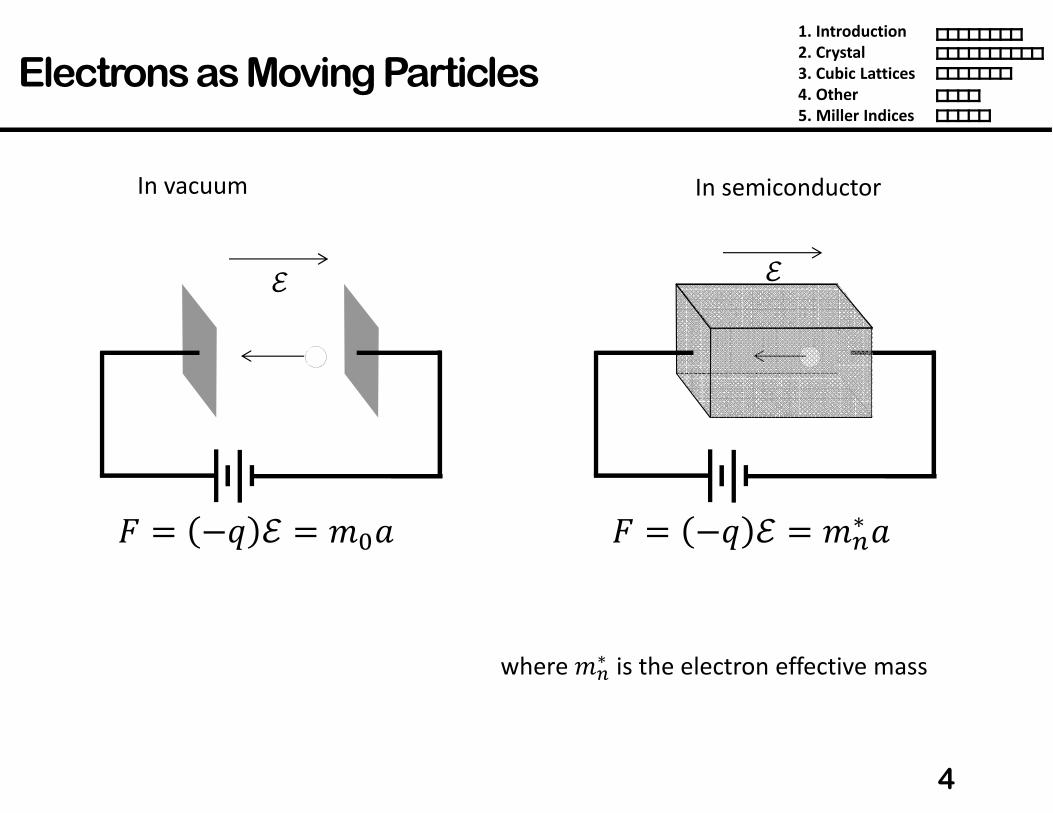
Electrons as Moving Particles
4
In semiconductor
� � �� � � ���
where �∗ is the electron effective mass
�
In vacuum
� � �� � � �∗�
�

1. Introduction
2. Crystal
3. Cubic Lattices
4. Other
5. Miller Indices
Thermal Velocity
5
We saw that:
In an electric field, �, an electron or a hole accelerates
electron and hole effective masses
32 �� � 1
2�∗����������
12 ��
� � 32��
��� � 3���∗ � 3 � 0.026�� � 1.6 � 10� !"/��
0.26 � 9.1 � 10�% &'� 2.3 � 10(� )⁄ � 2.3 � 10+ ,� )⁄
electrons:
holes:
� � ����∗
� � ���-∗
Si Ge GaAs
�∗ ��⁄ 0.26 0.12 0.068
�-∗ ��⁄ 0.39 0.3 0.5
Average electron kinetic energy=

1. Introduction
2. Crystal
3. Cubic Lattices
4. Other
5. Miller Indices
Carrier Scattering
6
Mobile electrons and atoms in the Si lattice are always in random thermal motion.
Electrons make frequent collisions with the vibrating atoms called “lattice
scattering” or “phonon scattering” (increases with increasing temperature)
Average velocity of thermal motion for electrons: ~107 cm/s @ 300K
electron1
23
4
5
Other scattering mechanisms:
deflection by ionized impurity atoms
deflection due to Columbic force between carriers (carrier-carrier scattering)
only significant at high carrier concentrations
The net current in any direction is zero, if no electric field is applied.

1. Introduction
2. Crystal
3. Cubic Lattices
4. Other
5. Miller Indices
Carrier Drift
7
When an electric field (e.g. due to an externally applied voltage) is applied to a
semiconductor, mobile charge carriers will be accelerated by the electrostatic
force. This force superimposes on the random motion of electrons:
electron1
23
4
5
Electrons drift in the direction opposite to the electric field
� current flows
Because of scattering, electrons in a semiconductor do not achieve
constant acceleration. However, they can be viewed as quasi-classical
particles moving at a constant average drift velocity �.
electron
123
4
5
�
1. Introduction
2. Crystal
3. Cubic Lattices
4. Other
5. Miller Indices
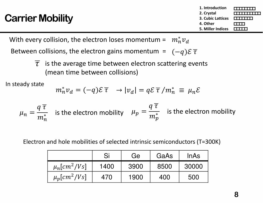
Carrier Mobility
8
Electron and hole mobilities of selected intrinsic semiconductors (T=300K)
With every collision, the electron loses momentum =
is the average time between electron scattering events
(mean time between collisions)
is the electron mobility
In steady state
�∗�.Between collisions, the electron gains momentum = /��0�12
12�∗�. � /��0�12 → �. � ��12 �∗⁄ ≡ 5�
5 � �12�∗
is the electron mobility5- � �12�-∗
Si Ge GaAs InAs
5[,��/�)] 1400 3900 8500 30000
5-[,��/�)] 470 1900 400 500

1. Introduction
2. Crystal
3. Cubic Lattices
4. Other
5. Miller Indices
Mean Free Path
9
Average distance traveled between collisions is called mean free path
This is an important length, structures at the order or smaller that m.f.p.
show different performance.
6 � ���12

1. Introduction
2. Crystal
3. Cubic Lattices
4. Other
5. Miller Indices
Mechanisms of Carrier Scattering
10
Dominant scattering mechanisms:
5-�77 ∝ 1-�77 ∝
Phonon scattering (lattice scattering) Impurity (dopant) ion scattering
Phonon scattering mobility
decreases when T increases:
There is less change in the electron’s
direction of travel if the electron zips
by the ion at a higher speed.
1phonondensity � carrierthermalvelocity
∝ 1� � � � ∝ ��%/�
��� ∝ �
--
-
+
Boron Ion
Arsenic
Ion
5-�77 ∝ ���%IJ K IL ∝ �%/�IJ K IL

1. Introduction
2. Crystal
3. Cubic Lattices
4. Other
5. Miller Indices
Matthiessen’sRule
11
The probability that a carrier will be scattered by mechanismMwithin a time period NO is NO/1� , where 1�is the mean time between scattering events due to mechanism M.Hence, The probability that a carrier will be scattered within a time period NO is
Temperature
Effect on
Mobility:
PNO/1�11 �
11-�77 K
11�Q-
→ 15 �1
5-�77 K1
5�Q-

1. Introduction
2. Crystal
3. Cubic Lattices
4. Other
5. Miller Indices
Mobility Dependence on Doping (Si)
12

1. Introduction
2. Crystal
3. Cubic Lattices
4. Other
5. Miller Indices
Velocity Saturation
13
108
107
106
105
102 103 104 105106
GaAs
Si
electrons
holes
�/�/,�0
� ./,�
/)0Carrier velocity vs. electric field

1. Introduction
2. Crystal
3. Cubic Lattices
4. Other
5. Miller Indices
Drift Velocity
14
= volume from which all holes cross plane in time O�.OR �
K
�.O
SR
= # of holes crossing plane in time OT�.OR= charge crossing plane in time O�T�.OR
= charge crossing plane per unit time
= hole current
�T�.R� Hole current per unit area = "- � S
R � �T�."_.V�W� � ��X�. � �X5�"-_.V�W� � ��T�.- � �T5-�".V�W� � "_.V�W� K "-_.V�W� � �X5 K �T5- � � Y�
Y ≡ �X5 K �T5-Conductivity of a semiconductor is
Resistivity Z ≡ 1 Y⁄ (Unit: ohm-cm)

1. Introduction
2. Crystal
3. Cubic Lattices
4. Other
5. Miller Indices
Resistivity vs. Doping
15
For n-type material:
Z ≅ 1�X5
Note: This
plot does not
apply to the
compensated
material!
For p-type material:
Z ≅ 1�T5-

1. Introduction
2. Crystal
3. Cubic Lattices
4. Other
5. Miller Indices
Electrical Resistance
16
Resistance (Ohms) K� �Y � 1
Z �"� � S \O⁄
� ]⁄ → ^ ≡ �S � Z ]
\Ohomogeneously
doped sample
Q: Consider a Si sample doped with 10 _/,�% Boron. What is its resistivity?
Z � 1�X5 K �T5- ~
1�T5-� 1.6 � 10� ! � 10 _ � 450 �
� 1.4Ω,�
S\ O
]
A: IJ � 10 _/,�%, IL � 0 (IJ ≫ ILhence p-type) T e 10 _/,�%and X e 10f/,�%
Q: Consider the same Si sample doped
with 10 +/,�% Arsenic. What is its
resistivity?
Z � 1�X5 K �T5- ~
1�X5� 1.6 � 10� ! � 9 � 10 _ � 650 �
� 0.12Ω,�
A: IJ � 10 _/,�%, IL � 10 +/,�%(IL ≫ IJ hence n-type) X e 9 � 10 _/,�%and T e 1.1 � 10%/,�%
1. Introduction
2. Crystal
3. Cubic Lattices
4. Other
5. Miller Indices
Potential vs. Kinetic Energy
17
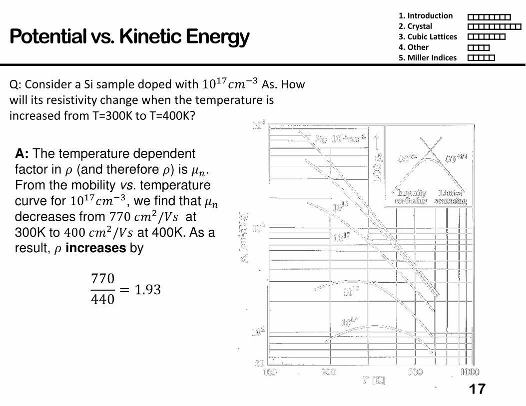
Q: Consider a Si sample doped with 10 +,��% As. How
will its resistivity change when the temperature is
increased from T=300K to T=400K?
770440 � 1.93
A: The temperature dependent
factor in Z (and therefore Z) is 5.
From the mobility vs. temperature
curve for 10 +,��%, we find that 5decreases from 770,��/�) at
300K to 400,��/�) at 400K. As a result, Z increases by

1. Introduction
2. Crystal
3. Cubic Lattices
4. Other
5. Miller Indices
Potential vs. Kinetic Energy
18
h. �. � �� � �reference
Valance band
Conduction band ��
��
j
�In
cre
asi
ng
ele
ctro
n e
ne
rgy
Incr
ea
sin
g h
ole
en
erg
yelectron K.E.
hole K.E.
�� represents the electron potential energy:
��
1. Introduction
2. Crystal
3. Cubic Lattices
4. Other
5. Miller Indices
Band Bending
19
��
K� �
��
j
����
� j
The potential energy of a particle with
charge ��is related to the electrostatic
potential �/j0:h. �. � ���� � 1
� /�ref. � ��0
� � �N�Nj � 1
�N��Nj
Variation of Ec with position is called
“band bending.”
1. Introduction
2. Crystal
3. Cubic Lattices
4. Other
5. Miller Indices
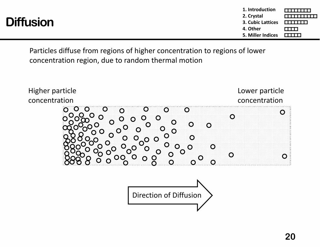
Diffusion
20
Particles diffuse from regions of higher concentration to regions of lower
concentration region, due to random thermal motion
Higher particle
concentration
Lower particle
concentration
Direction of Diffusion
1. Introduction
2. Crystal
3. Cubic Lattices
4. Other
5. Miller Indices
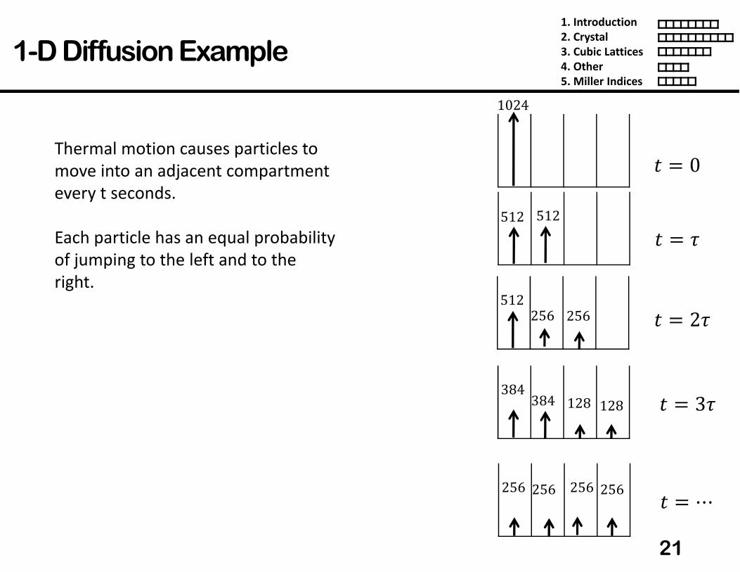
1-D Diffusion Example
21
Thermal motion causes particles to
move into an adjacent compartment
every t seconds.
Each particle has an equal probability
of jumping to the left and to the
right.
1024
512 512
512 256 256
384 384 128 128
O � 0
O � 1
O � 21
O � 31
256 256 O � ⋯256 256
1. Introduction
2. Crystal
3. Cubic Lattices
4. Other
5. Miller Indices
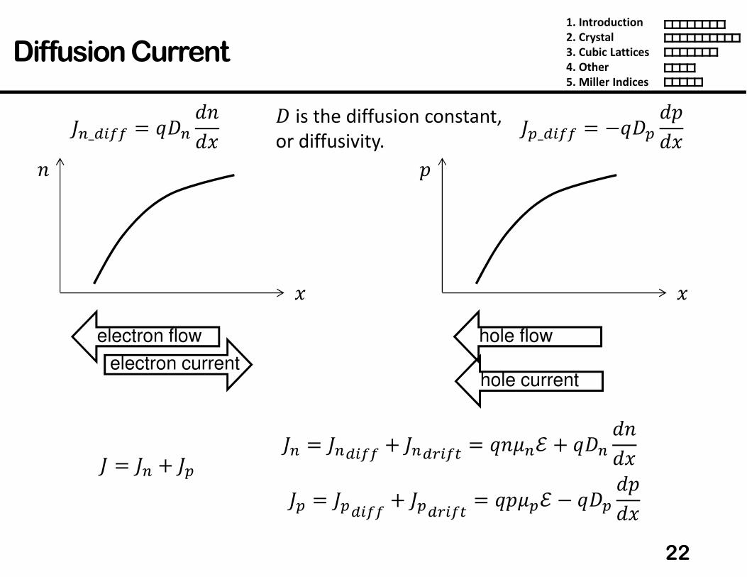
Diffusion Current
22
electron flow
"_.�WW � �n NXNj "-_.�WW � ��n- NTNjX
j
electron current
n is the diffusion constant,
or diffusivity.
hole flow
T
j
hole current
" � " K "- " � ".�WW K ".V�W� � �X5� K �n NXNj"- � "-.�WW K "-.V�W� � �T5-� � �n- NTNj

1. Introduction
2. Crystal
3. Cubic Lattices
4. Other
5. Miller Indices
Einstein Relationship
23
Consider a piece of a non-uniformly doped semiconductor:
�oIn equilibrium, �p is constant; therefore,
the band energies vary with position:
���p
In equilibrium, there is no net flow of
electrons or holes
" � 0�XN"- � 0
The drift and diffusion current components must balance each other exactly.
(A built-in electric field exists, such that the drift current exactly cancels out
the diffusion current due to the concentration gradient.)
" � �X5� K �n NXNj

1. Introduction
2. Crystal
3. Cubic Lattices
4. Other
5. Miller Indices
Non Uniformly Doped Semiconductor
24
The position of EF relative to the band edges is determined by the carrier concentrations,
which is determined by the dopant concentrations.
�o
��
�p
Under equilibrium conditions:
X � I� ��/qr�qs0 tu⁄n-type semiconductor
" � �X5� K �n NXNj � 0 � �X5� � �n X�� ��
Decreasing donor concentration
NXNj � �I����� qr�qs tu⁄ N��Nj
� � X��
N��Nj � � X�� ��
" � 0�XN"- � 0→ n� ��
� 5→ n-� ��
� 5-Similarly:
Note: The Einstein relationship is valid for a non-degenerate semiconductor,
even under non-equilibrium conditions
��
1. Introduction
2. Crystal
3. Cubic Lattices
4. Other
5. Miller Indices
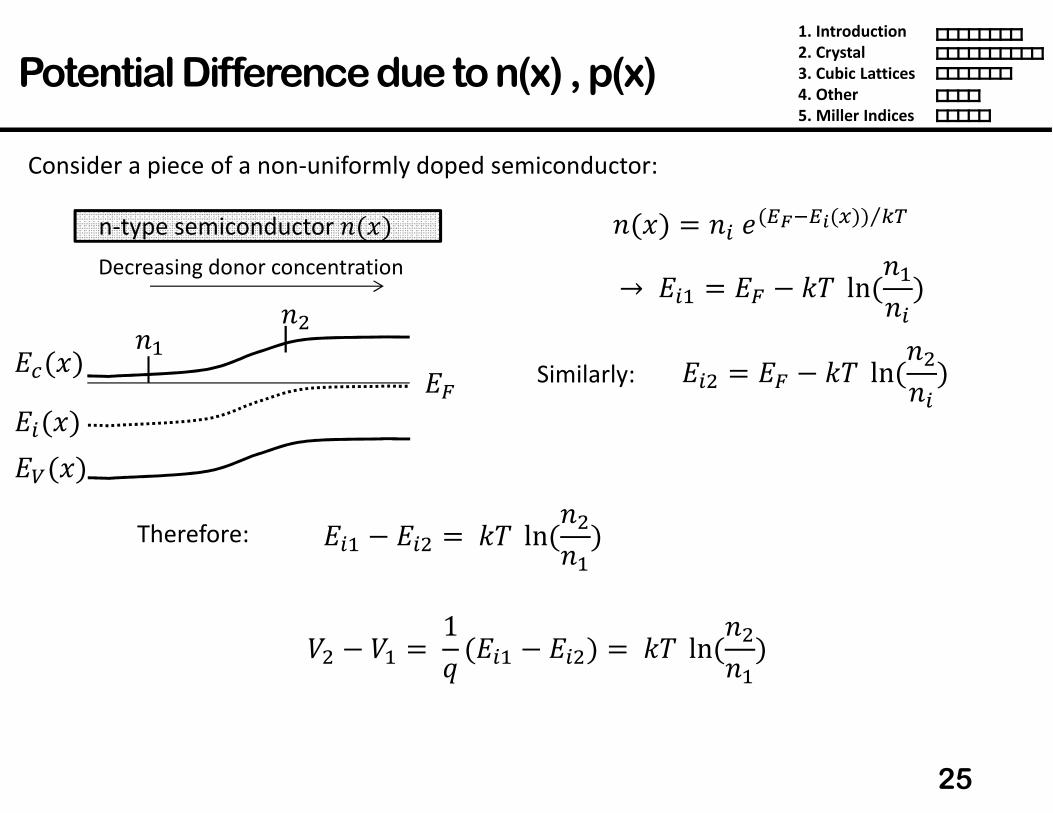
Potential Difference due to n(x) , p(x)
25
Consider a piece of a non-uniformly doped semiconductor:
�o/j0
��/j0�p
Therefore:
n-type semiconductor X/j0Decreasing donor concentration
��/j0X X�
X/j0 � X� �/qs�qv/w00 tu⁄
→ �� � �p � �� ln/X X� 0��� � �p � �� ln/X�X� 0Similarly:
�� � ��� � �� ln/X�X 0
�� � � �1� /�� � ���0 � �� ln/X�X 0
1. Introduction
2. Crystal
3. Cubic Lattices
4. Other
5. Miller Indices
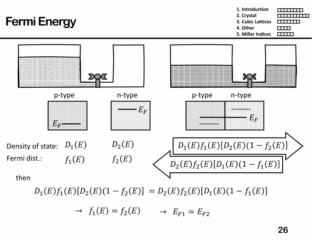
Fermi Energy
26
Density of state:
then
n � n � x � n� � /1 � x� �
�p�p
n-typep-type n-typep-type
�pn� �
Fermi dist.: x � x� � n� � x� � n � /1 � x �n � x � n� � /1 � x� � � n� � x� � n � /1 � x �
→ x � � x� � → �p � �p�
1. Introduction
2. Crystal
3. Cubic Lattices
4. Other
5. Miller Indices
27

1. Introduction
2. Crystal
3. Cubic Lattices
4. Other
5. Miller Indices
Non-Equilibrium Process
28
��
��
Whenever the thermal-equilibrium condition of a semiconductor system is disturbed
TX y X�� processes exist to restore the system to equilibrium
Generation and recombination processes act to change the carrier
concentrations, and thereby indirectly affect current flow
Recombination mechanisms: TX z X�� Generation mechanisms: TX { X��Direct
��
��Photon
(light)
R-G Center
�u Thermal
energy
��
��
Auger
Band-to-band
��
��
Photon
��
��
R-G Center
Thermal
energy �u
��
��
Impact Ionization
Recombination in Si is
primarily via R-G centers

1. Introduction
2. Crystal
3. Cubic Lattices
4. Other
5. Miller Indices
Recombination Mechanisms
29
��
��
Direct or Band to Band:
Basis for light emission devices
Photon (single particle of light) or multiple phonons (single
quantum of lattice vibration – equivalent to saying thermal energy)
R-G Center:
Also known as Schockley-Read-Hall (SRH) recombination
Photon (single particle of light) or multiple phonons (single
quantum of lattice vibration – equivalent to saying thermal energy)
Note: Trap level, Two steps: 1st Carrier is trapped at a
defect/impurity, 2nd Carrier (opposite type) is attracted to the RG
center and annihilates the 1st carrier
��
��Photon
(light)
�u Thermal
energy
��
��
Auger:
Requires 3 particles, Two steps:
1st carrier and 2nd carrier of the same type collide instantly
annihilating the electron hole pair (1st and 3rd carrier).
The energy lost in he annihilation process is given o the 2nd carrier.
2nd carrier gives off a series of phonons until it’s energy returns to
equilibrium energy (E~Ec)
1. Introduction
2. Crystal
3. Cubic Lattices
4. Other
5. Miller Indices
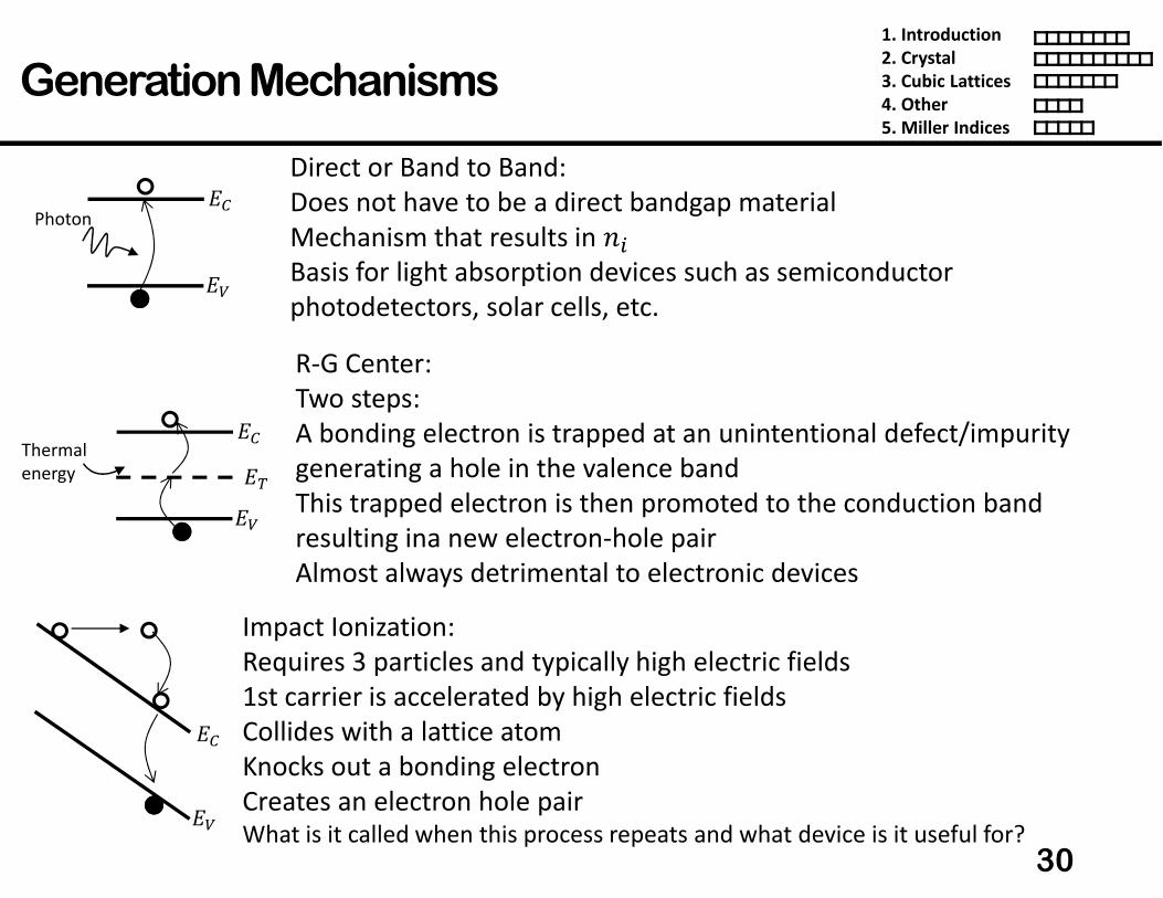
Generation Mechanisms
30
Direct or Band to Band:
Does not have to be a direct bandgap material
Mechanism that results in X�Basis for light absorption devices such as semiconductor
photodetectors, solar cells, etc.
R-G Center:
Two steps:
A bonding electron is trapped at an unintentional defect/impurity
generating a hole in the valence band
This trapped electron is then promoted to the conduction band
resulting ina new electron-hole pair
Almost always detrimental to electronic devices
Impact Ionization:
Requires 3 particles and typically high electric fields
1st carrier is accelerated by high electric fields
Collides with a lattice atom
Knocks out a bonding electron
Creates an electron hole pairWhat is it called when this process repeats and what device is it useful for?
��
��
Photon
��
��
Thermal
energy �u
��
��
1. Introduction
2. Crystal
3. Cubic Lattices
4. Other
5. Miller Indices
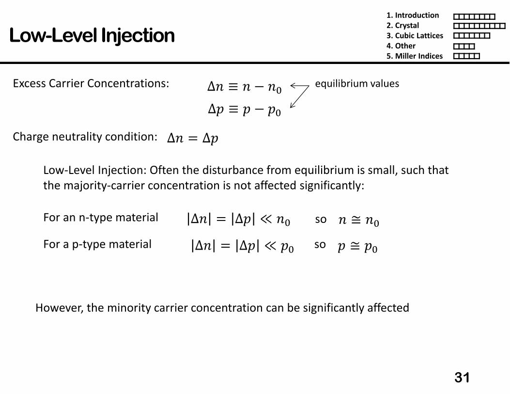
Low-Level Injection
31
Low-Level Injection: Often the disturbance from equilibrium is small, such that
the majority-carrier concentration is not affected significantly:
∆X ≡ X � X�Excess Carrier Concentrations:
∆T ≡ T � T�equilibrium values
Charge neutrality condition: ∆X � ∆T
For an n-type material
For a p-type material
∆X � ∆T ≪ X�∆X � ∆T ≪ T�
so X ≅ X�T ≅ T�so
However, the minority carrier concentration can be significantly affected

1. Introduction
2. Crystal
3. Cubic Lattices
4. Other
5. Miller Indices
Indirect Recombination Rate
32
Suppose excess carriers are introduced into an n-type Si sample (e.g. by temporarily
shining light onto it) at time t = 0. How does p vary with time t > 0?
1. Consider the rate of hole recombination via traps:
~T~O�� � �,-IuT Capture coefficient
2. Under low-level injection conditions, the hole generation rate is not significantly affected:
3. The net rate of change in T is therefore
,- �Iu � # or traps
~T~O�� ≅ ~T
~O�����v�.� �~T
~O�����v�.� �,-IuT�
~T~O���� �
~T~O�� K
~T~O�� � �,-IuT K ,-IuT� � �,-Iu/T � T�0
~T~O���� � ∆T
1- where1- ≡1
,-Iu

1. Introduction
2. Crystal
3. Cubic Lattices
4. Other
5. Miller Indices
Relaxation to Equilibrium State
33
Consider a semiconductor with no current flow in which thermal equilibrium is
disturbed by the sudden creation of excess holes and electrons. The system will relax
back to the equilibrium state via the R-G mechanism:
for electrons in p-type material:~X~O � �∆X1
The minority carrier lifetime 1 is the average time an excess minority carrier “survives”
in a sea of majority carriers.1 ranges from 1ns to 1ms in Si and depends on the density of metallic impurities
(contaminants) such as Au and Pt, and the density of crystalline defects. These deep
traps capture electrons or holes to facilitate recombination and are called
recombination-generation centers.
1 ≡ ,Iu �
for holes in n-type material:~T~O � �∆T1- 1- ≡ ,-Iu �

1. Introduction
2. Crystal
3. Cubic Lattices
4. Other
5. Miller Indices
Example: Photoconductor
34
Consider a sample of Si doped with 10 _,��%boron, with recombination lifetime 1μs.
It is exposed continuously to light, such that electron-hole pairs are generated
throughout the sample at the rate of 10�� per ,�% per second, i.e. the generation rate �� � 10��/,�%/)1. What are T� and X�? T� � 10 _cm�%X� � 10fcm�%
2. What are ∆X and ∆T? �� � ∆X 1⁄ � 10��∆X � ∆T � ��1 � 10�� � 10�_ � 10� f,��%
3. What are X and T? T � T� K ∆T � 10 _ K 10 f e 10 _,��%
X � X� K ∆X � 10f K 10 f e 10 f,��%
3. What is the XT product? XT � 10%�,��% ≫ X��

1. Introduction
2. Crystal
3. Cubic Lattices
4. Other
5. Miller Indices
Net Recombination Rate (General Case)
35
For arbitrary injection levels and both carrier types in a non-degenerate
semiconductor, the net rate of carrier recombination is:
For low level injection:
~∆X~O � ~∆T
~O � � TX � X��1- X K X K 1/T K T 0where and
~T~O � �∆T1-
X ≡ X��/q��qv0 tu⁄ T ≡ X� �/qv�q�0 tu⁄
~X~O � �∆X1for electrons in p-type material:
for holes in n-type material:

1. Introduction
2. Crystal
3. Cubic Lattices
4. Other
5. Miller Indices
Derivation of Continuity Equation
36
Consider carrier-flux into/out-of an infinitesimal volume:
Continuity Equation:
"/j0
Nj
"/j K Nj0
Area R, Volume RNj RNj ~X~O � �1
� " j R � " j K Nj R � ∆X1 RNj
" j K Nj � " j K ~"/j0~j Nj
→ ~X~O � 1�~"/j0~j � ∆X
1
~X~O � 1�
~"/j0~j � ∆X1 K ��
~T~O � �1�
~"-/j0~j � ∆T1- K ��
1. Introduction
2. Crystal
3. Cubic Lattices
4. Other
5. Miller Indices
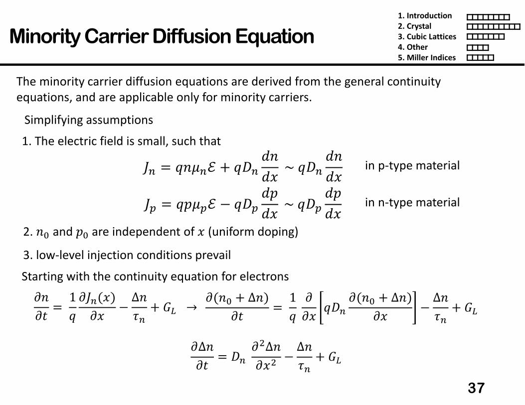
Minority Carrier Diffusion Equation
37
The minority carrier diffusion equations are derived from the general continuity
equations, and are applicable only for minority carriers.
Simplifying assumptions
2. X� and T� are independent of j (uniform doping)
3. low-level injection conditions prevail
in p-type material
1. The electric field is small, such that
" � �X5� K �n NXNj ~�nNXNj
"- � �T5-� � �n- NTNj ~�n-NTNj in n-type material
Starting with the continuity equation for electrons
~X~O � 1�
~"/j0~j � ∆X1 K �� → ~/X� K ∆X0
~O � 1� ~~j �n ~/X� K ∆X0
~j � ∆X1 K ��
~∆X~O � n ~
�∆X~j� � ∆X
1 K ��

1. Introduction
2. Crystal
3. Cubic Lattices
4. Other
5. Miller Indices
Minority Carrier Diffusion Equation
38
The subscript “X” or “T” is used to explicitly denote n-type or p-type material, e.g.T is the hole (minority-carrier) concentration in n-type materialX- is the electron (minority-carrier) concentration in p-type material
Simplifications (Special Cases):
Thus the minority carrier diffusion equations are
Steady state:
~∆X-~O � n ~�∆X-~j� � ∆X-1 K �� in p-type material
in n-type material~∆T~O � n- ~
�∆T~j� � ∆T1- K ��
~∆X-~O � 0 , ~∆T~O � 0No diffusion current:
n ~�∆X-~j� � 0, n- ~
�∆T~j� � 0
No R-G:
∆X-1 � 0, ∆T1- � 0No light:
�� � 0

1. Introduction
2. Crystal
3. Cubic Lattices
4. Other
5. Miller Indices
Example
39
Consider the special case:
1. constant minority-carrier (hole) injection at j � 02. steady state; no light absorption for j z 0:∆T 0 � ∆T0
�- is the hole diffusion length:
The general solution to the equation is
0 � n- ~�∆T~j� � ∆T1-
∆T j � R��w ��⁄ K ��w ��⁄
∆T ∞ � 0 → � � 0
where R, �are constants determined by
boundary conditions:
B.C.
Silicon bar
Light absorbed at x=0light
~�∆T~j� � ∆Tn-1- �∆T�-�j0 �- ≡ n-1-
∆T 0 � ∆T� → R � ∆T�Hence solution is:
∆T j � ∆T���w ��⁄
∆T∆T�
1 2 3 4 5
j �-⁄
1. Introduction
2. Crystal
3. Cubic Lattices
4. Other
5. Miller Indices
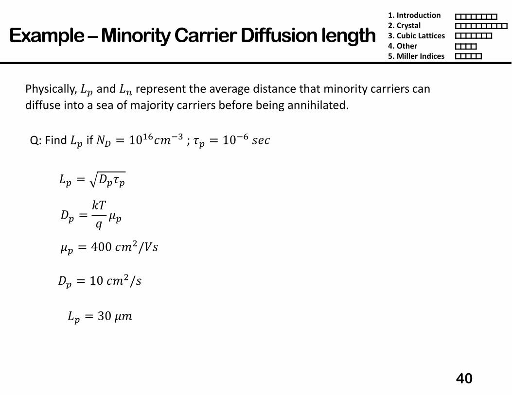
Example –Minority Carrier Diffusion length
40
Physically, �- and � represent the average distance that minority carriers can
diffuse into a sea of majority carriers before being annihilated.
Q: Find �- if IL � 10 _,��% ; 1- � 10�_)�,
n- � ��� 5-
n- � 10,��/)
�- � n-1-
�- � 305�
5- � 400,��/�)

1. Introduction
2. Crystal
3. Cubic Lattices
4. Other
5. Miller Indices
Quasi-Fermi Levels
41
Whenever ∆X � ∆T y 0, XT y X��. However, we would like to preserve and
use the relations:
These equations imply XT y X��, however. The solution is to introduce two
quasi-Fermi levels �� and �� such that
X � X��/qs�qv0 tu⁄ T � X��/qv�qs0 tu⁄
X � X��/p��qv0 tu⁄ T � X��/qv�p�0 tu⁄
�� � �� K �� ln XX� �� � �� � �� ln T
X�
1. Introduction
2. Crystal
3. Cubic Lattices
4. Other
5. Miller Indices
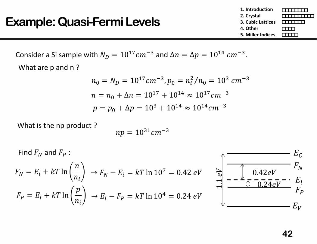
Example: Quasi-Fermi Levels
42
Consider a Si sample with IL � 10 +,��%and ∆X � ∆T � 10 f,��%.
What are p and n ?
�� � �� K �� ln XX�
X� � IL � 10 +,��%, T� � X�� X�⁄ � 10%,��%X � X� K ∆X � 10 + K 10 f e 10 +,��%T � T� K ∆T � 10% K 10 f e 10 f,��%
What is the np product ? XT � 10% ,��%
Find �� and �� :
→ �� � �� � �� ln10+ � 0.42���� � �� K �� ln T
X� → �� � �� � �� ln 10f � 0.24��
��
����1.1
��
����
0.42��0.24��