sgh-e250 - deblocage orange francedeblocage77.free.fr/sam/root/samsung sgh-e250...
TRANSCRIPT
GSM TELEPHONESGH-E250
GSM TELEPHONE CONTENTS
1. Safety Precautions
2. Specification
3. Product Function
4. Array course control
5. Exploded View/Disassemblyand Assembly Instructions
6. MAIN Electrical Parts List
7. Block Diagrams
8. PCB Diagrams
9. Flow Chart of Troubleshooting
10. Reference data
CONTENTS
1. Safety Precautions1-1. Repair Precaution......................................................................................................1-11-2. ESD(Electrostatically Sensitive Devices) Precaution...............................................1-2
2. Specification2-1. GSM General Specification.......................................................................................2-12-2. GSM Tx Power Class...............................................................................................2-2
3. Product Function
4. Array course control4-1. Sofrware Adjustments................................................................................................4-14-2. Sofrware Downloading .............................................................................................4-2
5. Exploded View/Disassembly & Assembly Instructions5-1. Cellular phone Exploded View..................................................................................5-15-2. Cellular phone Parts list............................................................................................5-25-3. Disassembly & Assembly Instructions......................................................................5-4
6. MAIN Electrical Parts List
7. Block Diagrams7-1. Base Band Block Diagram........................................................................................7-17-2. RF Block Diagram.....................................................................................................7-2
8. PCB Diagrams

CONTENTS
9. Flow Chart of Troubleshooting9-1. Pown on.....................................................................................................................9-19-2. Initial...........................................................................................................................9-39-3. Charging Part.............................................................................................................9-59-4. SIM Part.....................................................................................................................9-79-5. Microphone Part.........................................................................................................9-99-6. Speaker Part(Melody)..............................................................................................9-119-7. Key Data Input........................................................................................................9-139-8. Receiver Part...........................................................................................................9-149-9. Back Light(for Color Main LCD).............................................................................9-159-10. Key Back Light......................................................................................................9-179-11. Camera Part...........................................................................................................9-199-12. GSM Receiver........................................................................................................9-219-13. GSM Transmitter....................................................................................................9-229-14. DCS Receiver........................................................................................................9-239-15. DCS Transmitter....................................................................................................9-249-16. PCS Receiver.........................................................................................................9-259-17. PCS Transmitter.....................................................................................................9-269-18. Bluetooth Part........................................................................................................9-289-19. Radio Part..............................................................................................................9-30
10. Reference data
SAMSUNG Proprietary-Contents may change without notice
1. Safety Precautions
1-1
This Document can not be used without Samsung's authorization
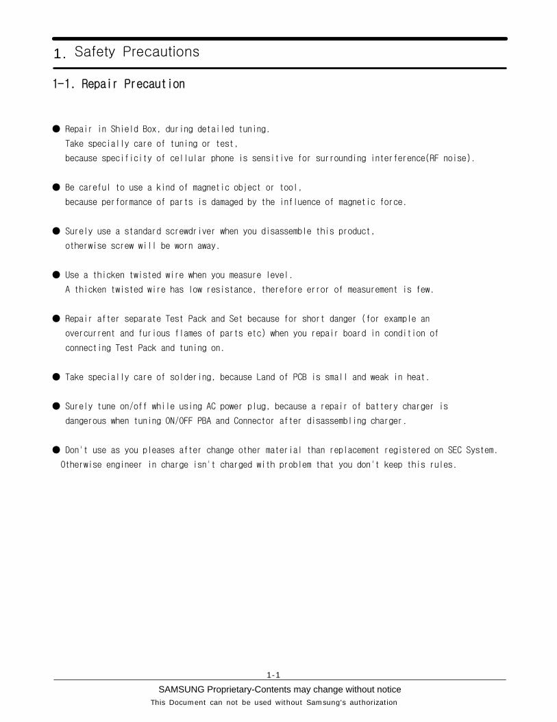
1-1. Repair Precaution
● Repair in Shield Box, during detailed tuning.
Take specially care of tuning or test,
because specificity of cellular phone is sensitive for surrounding interference(RF noise).
● Be careful to use a kind of magnetic object or tool,
because performance of parts is damaged by the influence of magnetic force.
● Surely use a standard screwdriver when you disassemble this product,
otherwise screw will be worn away.
● Use a thicken twisted wire when you measure level.
A thicken twisted wire has low resistance, therefore error of measurement is few.
● Repair after separate Test Pack and Set because for short danger (for example an
overcurrent and furious flames of parts etc) when you repair board in condition of
connecting Test Pack and tuning on.
● Take specially care of soldering, because Land of PCB is small and weak in heat.
● Surely tune on/off while using AC power plug, because a repair of battery charger is
dangerous when tuning ON/OFF PBA and Connector after disassembling charger.
● Don't use as you pleases after change other material than replacement registered on SEC System.
Otherwise engineer in charge isn't charged with problem that you don't keep this rules.
SAMSUNG Proprietary-Contents may change without notice
Safety Precautions
1-2
This Document can not be used without Samsung's authorization
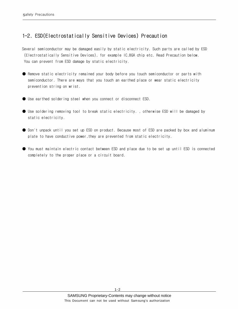
1-2. ESD(Electrostatically Sensitive Devices) Precaution
Several semiconductor may be damaged easily by static electricity. Such parts are called by ESD
(Electrostatically Sensitive Devices), for example IC,BGA chip etc. Read Precaution below.
You can prevent from ESD damage by static electricity.
● Remove static electricity remained your body before you touch semiconductor or parts with
semiconductor. There are ways that you touch an earthed place or wear static electricity
prevention string on wrist.
● Use earthed soldering steel when you connect or disconnect ESD.
● Use soldering removing tool to break static electricity. , otherwise ESD will be damaged by
static electricity.
● Don't unpack until you set up ESD on product. Because most of ESD are packed by box and aluminum
plate to have conductive power,they are prevented from static electricity.
● You must maintain electric contact between ESD and place due to be set up until ESD is connected
completely to the proper place or a circuit board.

2. Specification
2-1
2-1. GSM General Specification
GSM900Phase 1
EGSM 900Phase 2
DCS1800Phase 1 PCS1900
Freq.Band[MHz]
Upl ink/Downl ink
890~915935~960
880~915925~960
1710~17851805~1880
1850~19101930~1990
ARFCN range 1~124 0~124 &975~1023 512~885 512~810
Tx/Rx spacing 45MHz 45MHz 95MHz 80MHz
Mod. Bit rate/Bi t Per iod
270.833kbps3.692us
270.833kbps3.692us
270.833kbps3.692us
270.833kbps3.692us
Time SlotPeriod/Frame
Per iod
576.9us4.615ms
576.9us4.615ms
576.9us4.615ms
576.9us4.615ms
Modulat ion 0.3GMSK 0.3GMSK 0.3GMSK 0.3GMSK
MS Power 33dBm~5dBm 33dBm~5dBm 30dBm~0dBm 30dBm~0dBm
Power Class 5pcl ~ 19pcl 5pcl ~ 19pcl 0pcl ~ 15pcl 0pcl ~ 15pcl
Sensit iv i ty -102dBm -102dBm -100dBm -100dBm
TDMA Mux 8 8 8 8
Cell Radius 35Km 35Km 2Km -
Speclflcation
2-2
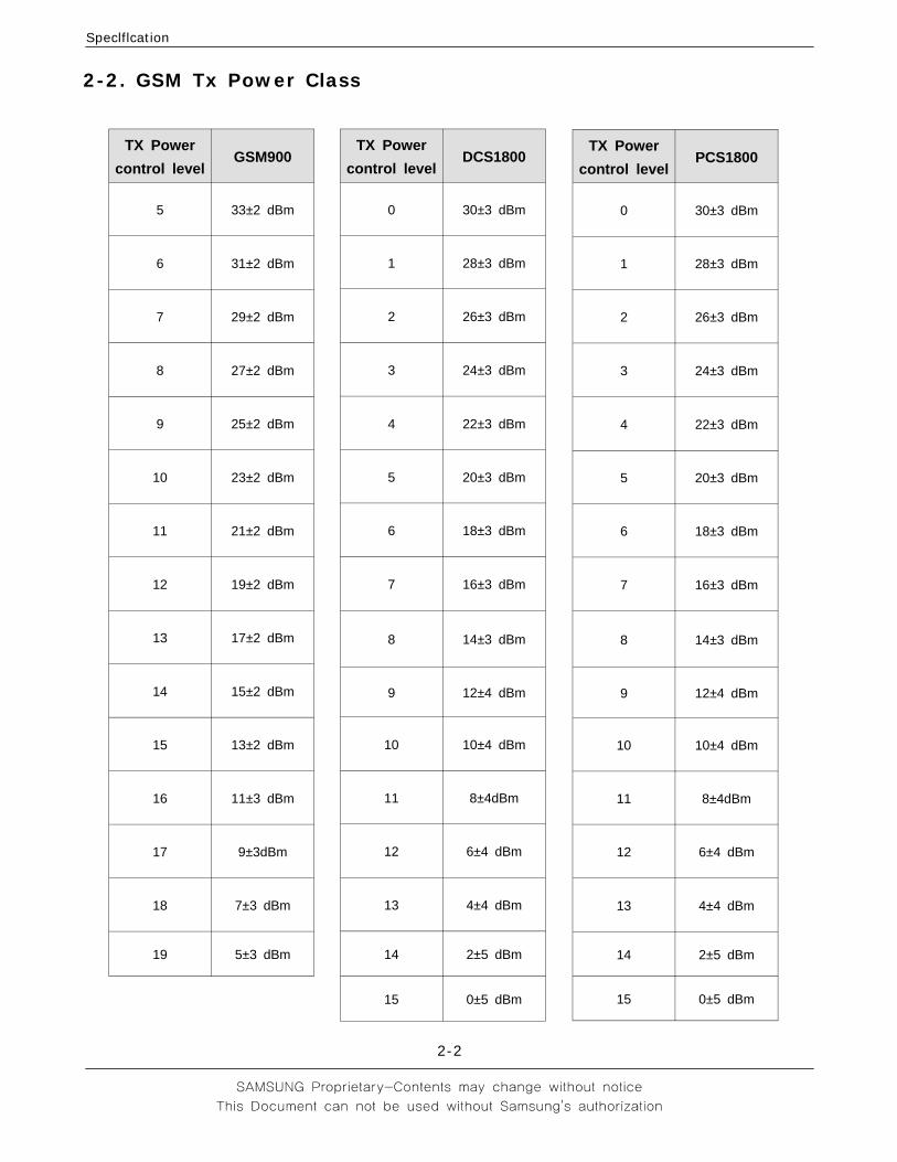
TX Powercontrol level
GSM900
5 33±2 dBm
6 31±2 dBm
7 29±2 dBm
8 27±2 dBm
9 25±2 dBm
10 23±2 dBm
11 21±2 dBm
12 19±2 dBm
13 17±2 dBm
14 15±2 dBm
15 13±2 dBm
16 11±3 dBm
17 9±3dBm
18 7±3 dBm
19 5±3 dBm
TX Powercontrol level
DCS1800
0 30±3 dBm
1 28±3 dBm
2 26±3 dBm
3 24±3 dBm
4 22±3 dBm
5 20±3 dBm
6 18±3 dBm
7 16±3 dBm
8 14±3 dBm
9 12±4 dBm
10 10±4 dBm
11 8±4dBm
12 6±4 dBm
13 4±4 dBm
14 2±5 dBm
15 0±5 dBm
TX Powercontrol level
PCS1800
0 30±3 dBm
1 28±3 dBm
2 26±3 dBm
3 24±3 dBm
4 22±3 dBm
5 20±3 dBm
6 18±3 dBm
7 16±3 dBm
8 14±3 dBm
9 12±4 dBm
10 10±4 dBm
11 8±4dBm
12 6±4 dBm
13 4±4 dBm
14 2±5 dBm
15 0±5 dBm
2-2. GSM Tx Power Class
SAMSUNG Proprietary-Contents may change without notice
3. Product Function
3-1
This Document can not be used without Samsung's authorization
Main Function
-SlimSlide Design Intenna-VGA Camera-Bluetooth V.2.0-Stereo Bluetooth Headset-Mobile Tracker & SOS Messaging-Large 2.0" 65K Color TFT Display-SMS/MMS/E-Mail-WAP 2.0 / Java MIDP 2.0-MP3, AAC, MP4, 3GPP Decoding-Video Recording and Messaging-GSM/GPRS Class 10-Triple Band(GSM900/DCS,PCS)-64 Poly-Speaker Phone-Voice Clarity
SAMSUNG Proprietary-Contents may change without notice
Product Function
3-2
This Document can not be used without Samsung's authorization
SAMSUNG Proprietary-Contents may change without notice
4. Array course control
4-1
This Document can not be used without Samsung's authorization
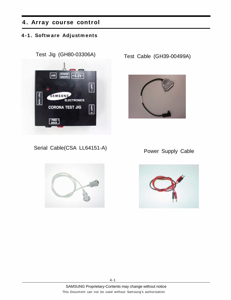
4-1. Software Adjustments
Power Supply CableSerial Cable(CSA LL64151-A)
Test Jig (GH80-03306A) Test Cable (GH39-00499A)

SAMSUNG Proprietary-Contents may change without notice
Array course control
4-2
This Document can not be used without Samsung's authorization
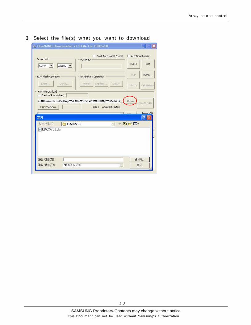
4-2. Software Downloading
4-2-1. Pre-requsite for Downloading
• Downloader Program(OneNAND Downloder V1.2 Lite For PNX5230.exe)• E250 Mobile Phone
• Data Cable
• Binary file, TFS file
4-2-2. S/W Downloader Program■ Load the binary download program by executing the
“OneNAND Downloder V1.2 Lite For PNX5230.exe”
1. Select the connected serial port and the rate of speed
2. Select the check box, the mode you want to download.
- if the binary file wanted, check only 'BIN'- if the tfs file wanted, check only 'TFS'- if all the files wanted, check 'BIN+TFS'
1
2
SAMSUNG Proprietary-Contents may change without notice
Array course control
4-3
This Document can not be used without Samsung's authorization
3. Select the file(s) what you want to download
SAMSUNG Proprietary-Contents may change without notice
Array course control
4-4
This Document can not be used without Samsung's authorization
SAMSUNG Proprietary-Contents may change without notice5-1
This Document can not be used without Samsung's authorization
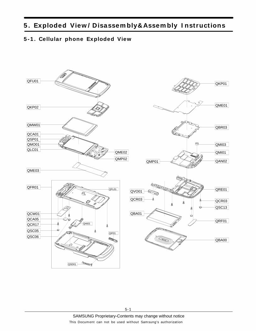
5. Exploded View/Disassembly&Assembly Instructions
5-1. Cellular phone Exploded View
QFU01
QKP02
QKP01
QMW01
QME03
QME02
QFR01
QCW01QCA05QCR17
QSC05QSC06
QSP01QMO01QLC01
QCA01
QSD01
QHI01
QIF01
QFL01
QME01
QBR03
QMI03
QMI01
QAN02QMP01
QRE01
QSC13
QRF01
QBA00
QCR03
QBA01
QVO01
QCR03
QMP02
SAMSUNG Proprietary-Contents may change without notice
Exploded View/Disassembly&Assembly Instructions
5-2
This Document can not be used without Samsung's authorization
5-2. Cellular phone Parts list
Design LOC Description Sec CodeQAN02 INTENNA-SGH E250 GH42-00985A
QBA00 ASSY CASE-BATTERY GH98-03586A
QBA01 INNER BATTERY PACK-750MAH,BLK, GH43-02483A
QBR03 ASSY BRACKET-KEYPAD GH98-02620A
QCA01 UNIT-CAMERA MODULE GH59-03619A
QCA05 PMO-DECO MIRROR GH72-34243A
QCR03 SCREW-MACHINE 6001-001811
QCR03 SCREW-MACHINE 6001-001811
QCR17 SCREW-MACHINE 6001-001460
QCW01 PCT-COVER WINDOW CAMERA GH72-34247A
QFU01 ASSY CASE-SLIDE UPPER GH98-02259A
QKP01 ASSY KEYPAD-MAIN(EU/SIL) GH98-02264A
QKP02 ASSY KEYPAD-SUB(EU/SIL) GH98-02263A
QME01 UNIT-KEY FPCB GH59-03615A
QME03 MEA-SLIDE FPCBKIT GH97-06873A
QMI01 MICROPHONE-ASSY GH30-00309A
QMI03 RMO-RUBBER MIC GH73-08308A
QMP01 PBA MAIN-SGH E250 MAIN GH92-03188A
QRE01 ASSY CASE-REAR GH98-02262A
QRF01 MPR-TAPE RF SHEET GH74-27453A
QSC05 RMO-RUBBER SCREW SLIDE L GH73-08309A
QSC06 RMO-RUBBER SCREW SLIDE R GH73-08310A
QSC13 RMO-RUBBER SCREW REAR GH73-08311A
QVO01 PMO-VOLUME KEY GH72-34246A
QLC01 LCD-SGH E250 MODULE GH07-01018A
QMW01 ASSY COVER-WINDOW MAIN GH98-02619A
QSP01 SPEAKER 3001-002061
QMO01 MOTOR DC-SCHF509 GH31-00249A
QMP02 PBA SUB-SGH E250 PCB GH92-03393A QME02 UNIT-METAL DOME GH59-03617A
QFR01 ASSY CASE-F/C+S/L GH98-02261A QFL01 ASSY CASE-SLIDE LOWER GH98-02260A QHI01 ASSY HINGE-PUSH ROD GH98-03165A QIF01 PMO-COVER IF GH72-34244A QSD01 PMO-COVER M SD GH72-34245A
SAMSUNG Proprietary-Contents may change without notice
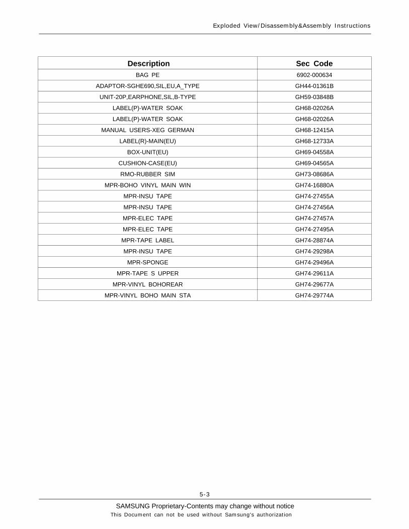
Exploded View/Disassembly&Assembly Instructions
5-3
This Document can not be used without Samsung's authorization
Description Sec CodeBAG PE 6902-000634
ADAPTOR-SGHE690,SIL,EU,A_TYPE GH44-01361B
UNIT-20P,EARPHONE,SIL,B-TYPE GH59-03848B
LABEL(P)-WATER SOAK GH68-02026A
LABEL(P)-WATER SOAK GH68-02026A
MANUAL USERS-XEG GERMAN GH68-12415A
LABEL(R)-MAIN(EU) GH68-12733A
BOX-UNIT(EU) GH69-04558A
CUSHION-CASE(EU) GH69-04565A
RMO-RUBBER SIM GH73-08686A
MPR-BOHO VINYL MAIN WIN GH74-16880A
MPR-INSU TAPE GH74-27455A
MPR-INSU TAPE GH74-27456A
MPR-ELEC TAPE GH74-27457A
MPR-ELEC TAPE GH74-27495A
MPR-TAPE LABEL GH74-28874A
MPR-INSU TAPE GH74-29298A
MPR-SPONGE GH74-29496A
MPR-TAPE S UPPER GH74-29611A
MPR-VINYL BOHOREAR GH74-29677A
MPR-VINYL BOHO MAIN STA GH74-29774A
SAMSUNG Proprietary-Contents may change without notice
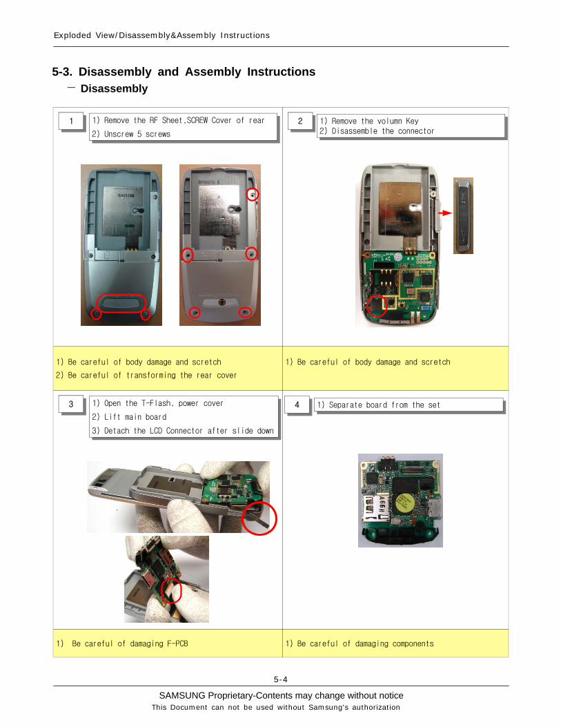
Exploded View/Disassembly&Assembly Instructions
5-4
This Document can not be used without Samsung's authorization
1) Be careful of body damage and scretch
2) Be careful of transforming the rear cover
1) Be careful of body damage and scretch
1) Be careful of damaging F-PCB 1) Be careful of damaging components
1) Remove the RF Sheet,SCREW Cover of rear
2) Unscrew 5 screws
1 1) Remove the volumn Key2) Disassemble the connector
2
3 1) Open the T-Flash, power cover
2) Lift main board
3) Detach the LCD Connector after slide down
4 1) Separate board from the set
5-3. Disassembly and Assembly Instructions― Disassembly
SAMSUNG Proprietary-Contents may change without notice
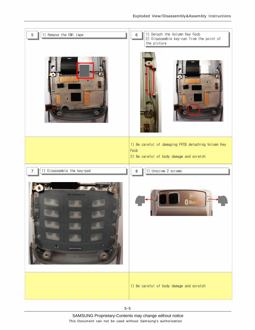
Exploded View/Disassembly&Assembly Instructions
5-5
This Document can not be used without Samsung's authorization
1) Be careful of damaging FPCB detaching Volumn Key
Fpcb
2) Be careful of body damage and scretch
1) Be careful of body damage and scretch
5 6
7 8
1) Remove the EMI tape 1) Detach the Volumn Key Fpcb2) Disassemble key-can from the point ofthe picture
1) Disassemble the key-pad 1) Unscrew 2 screws
SAMSUNG Proprietary-Contents may change without notice
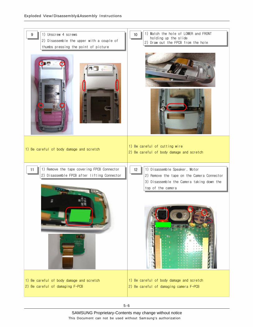
Exploded View/Disassembly&Assembly Instructions
5-6
This Document can not be used without Samsung's authorization
1) Be careful of body damage and scretch1) Be careful of cutting wire
2) Be careful of body damage and scretch
1) Be careful of body damage and scretch
2) Be careful of damaging F-PCB
1) Be careful of body damage and scretch
2) Be careful of damaging camera F-PCB
9 10
11 12
1) Unscrew 4 screws
2) Disassemble the upper with a couple of
thumbs pressing the point of picture
1) Match the hole of LOWER and FRONTholding up the slide
2) Draw out the FPCB from the hole
1) Remove the tape covering FPCB Connector
2) Disassemble FPCB after lifting Connector
1) Disassemble Speaker, Motor
2) Remove the tape on the Camera Connector
3) Disassemble the Camera taking down the
top of the camera
SAMSUNG Proprietary-Contents may change without notice
Exploded View/Disassembly&Assembly Instructions
5-7
This Document can not be used without Samsung's authorization
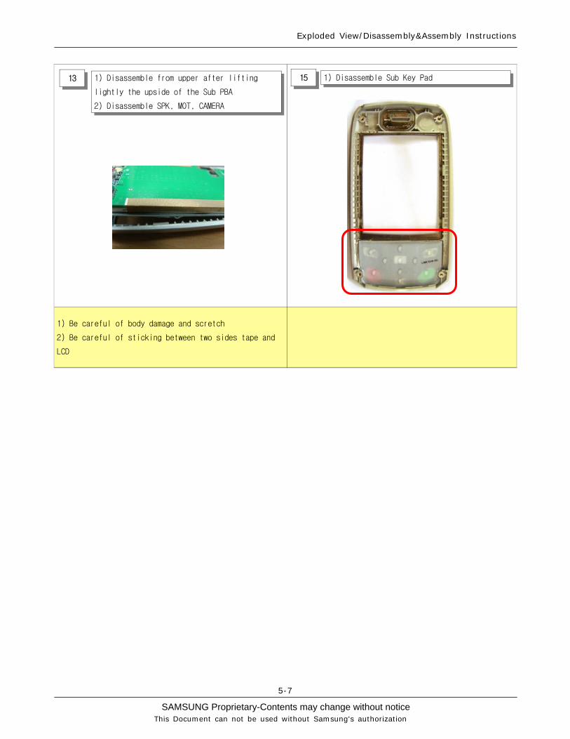
1) Be careful of body damage and scretch
2) Be careful of sticking between two sides tape and
LCD
13 1) Disassemble from upper after lifting
lightly the upside of the Sub PBA
2) Disassemble SPK, MOT, CAMERA
1) Disassemble Sub Key Pad15
SAMSUNG Proprietary-Contents may change without notice
Exploded View/Disassembly&Assembly Instructions
5-8
This Document can not be used without Samsung's authorization
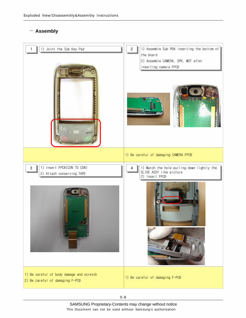
1) Be careful of damaging CAMERA FPCB
1) Be careful of body damage and scretch
2) Be careful of damaging F-PCB1) Be careful of damaging F-PCB
1 2
3 4
1) Joint the Sub Key Pad 1) Assemble Sub PBA inserting the bottom of
the board
2) Assemble CAMERA, SPK, MOT after
inserting camera FPCB
1) Insert FPCB(CON TO CON)
2) Attach conserving TAPE
1) Match the hole pulling down lightly theSLIDE ASSY like picture2) Insert FPCB
― Assembly
SAMSUNG Proprietary-Contents may change without notice
Exploded View/Disassembly&Assembly Instructions
5-9
This Document can not be used without Samsung's authorization
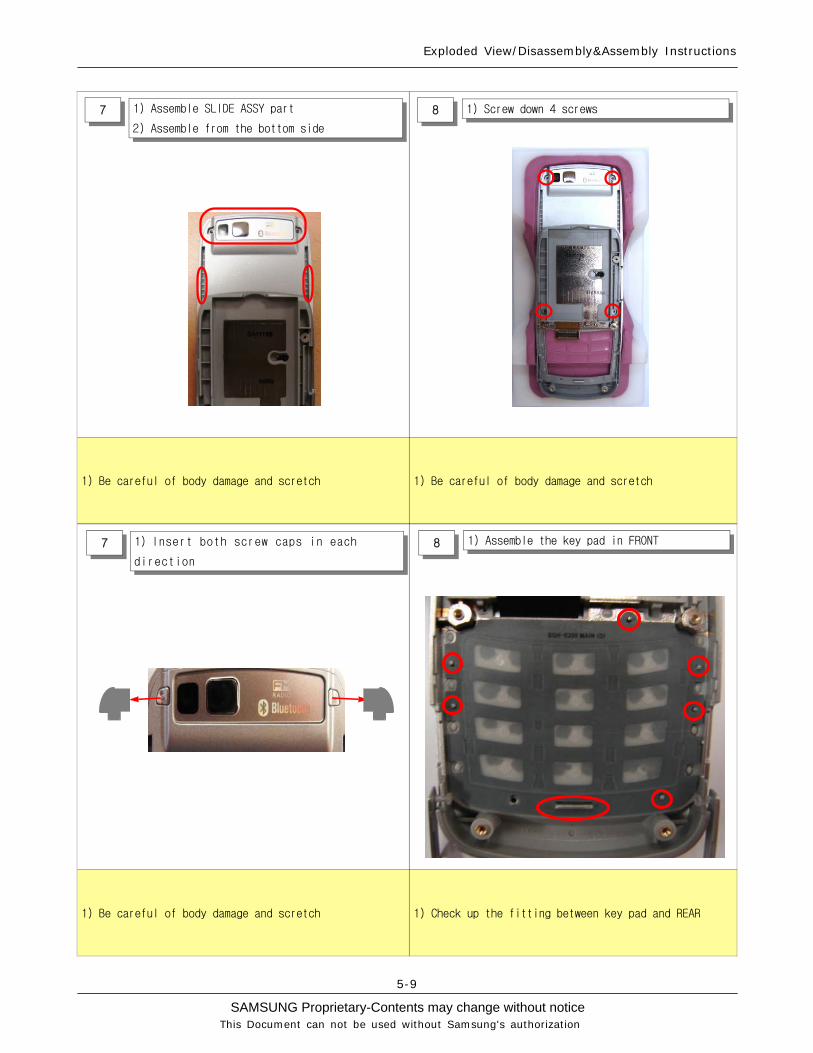
1) Be careful of body damage and scretch 1) Be careful of body damage and scretch
1) Be careful of body damage and scretch 1) Check up the fitting between key pad and REAR
7 81) Insert both screw caps in each
direction
1) Assemble the key pad in FRONT
7 81) Assemble SLIDE ASSY part
2) Assemble from the bottom side
1) Screw down 4 screws
SAMSUNG Proprietary-Contents may change without notice
Exploded View/Disassembly&Assembly Instructions
5-10
This Document can not be used without Samsung's authorization
1) Be careful of damaging F-PCB1) Check up whether tape color is same with SET color
or not
1) Be careful of damaging BGA components 1) Be careful of body damage and scretch
109 1) Attach the EMI tape1) Assemble the key can
2) Check up the attaching FPCB in Volumn
Key side
11 121) Assemble the FPCB with main board 1) Open the T-Flash, Power Cover
2) Assemble the main board
SAMSUNG Proprietary-Contents may change without notice
Exploded View/Disassembly&Assembly Instructions
5-11
This Document can not be used without Samsung's authorization
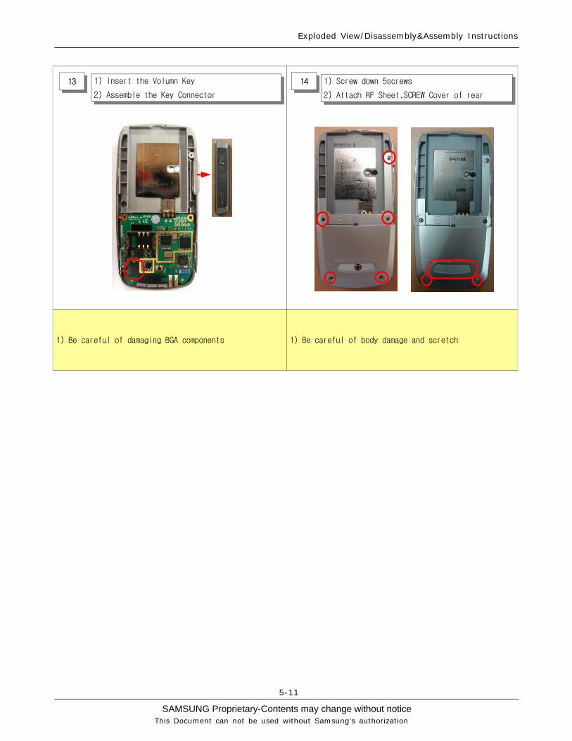
1) Be careful of damaging BGA components 1) Be careful of body damage and scretch
13 1) Insert the Volumn Key
2) Assemble the Key Connector
1) Screw down 5screws
2) Attach RF Sheet,SCREW Cover of rear
14
SAMSUNG Proprietary-Contents may change without notice
Exploded View/Disassembly&Assembly Instructions
5-12
This Document can not be used without Samsung's authorization
SAMSUNG Proprietary-Contents may change without notice
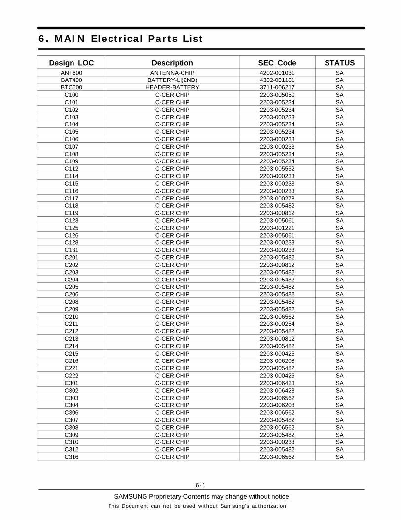
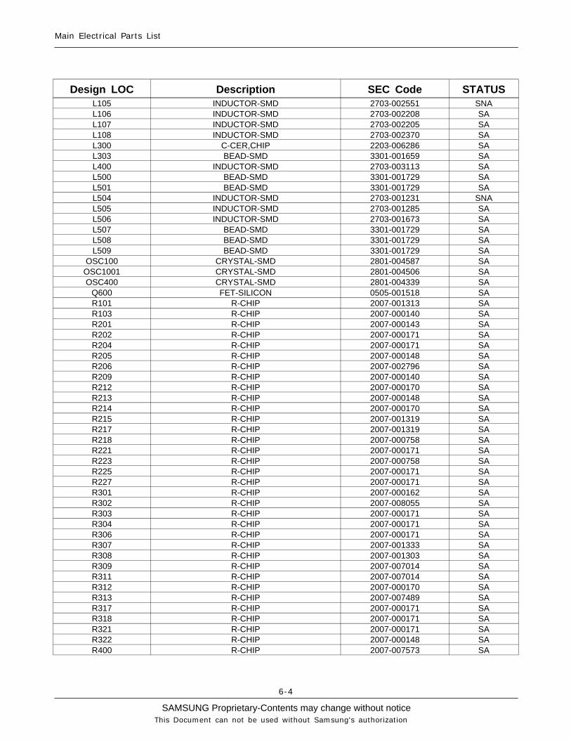
6. MAIN Electrical Parts List
6-1
This Document can not be used without Samsung's authorization
Design LOC Description SEC Code STATUSANT600 ANTENNA-CHIP 4202-001031 SABAT400 BATTERY-LI(2ND) 4302-001181 SABTC600 HEADER-BATTERY 3711-006217 SA
C100 C-CER,CHIP 2203-005050 SAC101 C-CER,CHIP 2203-005234 SAC102 C-CER,CHIP 2203-005234 SAC103 C-CER,CHIP 2203-000233 SAC104 C-CER,CHIP 2203-005234 SAC105 C-CER,CHIP 2203-005234 SAC106 C-CER,CHIP 2203-000233 SAC107 C-CER,CHIP 2203-000233 SAC108 C-CER,CHIP 2203-005234 SAC109 C-CER,CHIP 2203-005234 SAC112 C-CER,CHIP 2203-005552 SAC114 C-CER,CHIP 2203-000233 SAC115 C-CER,CHIP 2203-000233 SAC116 C-CER,CHIP 2203-000233 SAC117 C-CER,CHIP 2203-000278 SAC118 C-CER,CHIP 2203-005482 SAC119 C-CER,CHIP 2203-000812 SAC123 C-CER,CHIP 2203-005061 SAC125 C-CER,CHIP 2203-001221 SAC126 C-CER,CHIP 2203-005061 SAC128 C-CER,CHIP 2203-000233 SAC131 C-CER,CHIP 2203-000233 SAC201 C-CER,CHIP 2203-005482 SAC202 C-CER,CHIP 2203-000812 SAC203 C-CER,CHIP 2203-005482 SAC204 C-CER,CHIP 2203-005482 SAC205 C-CER,CHIP 2203-005482 SAC206 C-CER,CHIP 2203-005482 SAC208 C-CER,CHIP 2203-005482 SAC209 C-CER,CHIP 2203-005482 SAC210 C-CER,CHIP 2203-006562 SAC211 C-CER,CHIP 2203-000254 SAC212 C-CER,CHIP 2203-005482 SAC213 C-CER,CHIP 2203-000812 SAC214 C-CER,CHIP 2203-005482 SAC215 C-CER,CHIP 2203-000425 SAC216 C-CER,CHIP 2203-006208 SAC221 C-CER,CHIP 2203-005482 SAC222 C-CER,CHIP 2203-000425 SAC301 C-CER,CHIP 2203-006423 SAC302 C-CER,CHIP 2203-006423 SAC303 C-CER,CHIP 2203-006562 SAC304 C-CER,CHIP 2203-006208 SAC306 C-CER,CHIP 2203-006562 SAC307 C-CER,CHIP 2203-005482 SAC308 C-CER,CHIP 2203-006562 SAC309 C-CER,CHIP 2203-005482 SAC310 C-CER,CHIP 2203-000233 SAC312 C-CER,CHIP 2203-005482 SAC316 C-CER,CHIP 2203-006562 SA
SAMSUNG Proprietary-Contents may change without notice
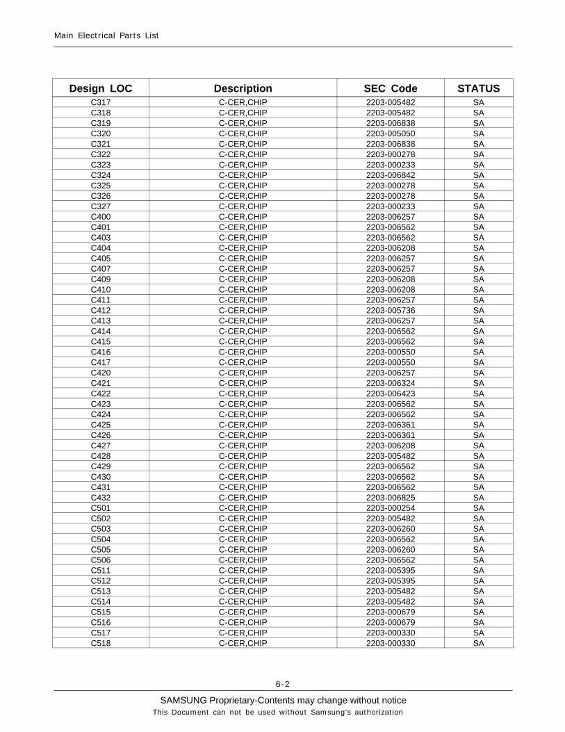
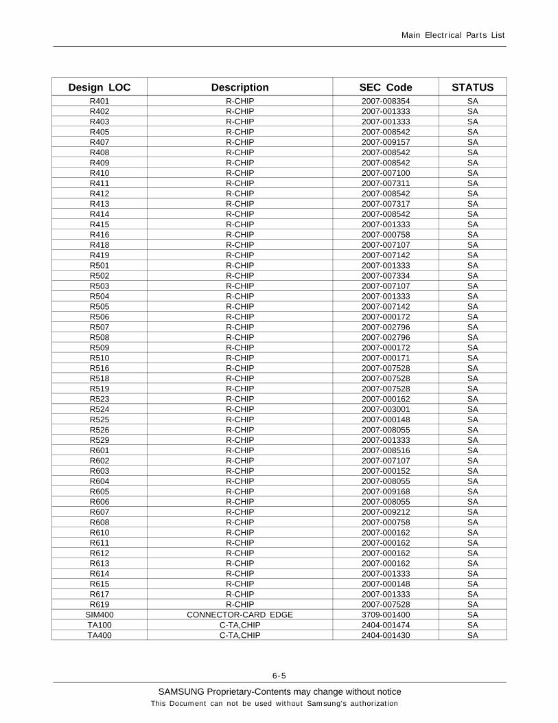
Main Electrical Parts List
6-2
This Document can not be used without Samsung's authorization
Design LOC Description SEC Code STATUSC317 C-CER,CHIP 2203-005482 SAC318 C-CER,CHIP 2203-005482 SAC319 C-CER,CHIP 2203-006838 SAC320 C-CER,CHIP 2203-005050 SAC321 C-CER,CHIP 2203-006838 SAC322 C-CER,CHIP 2203-000278 SAC323 C-CER,CHIP 2203-000233 SAC324 C-CER,CHIP 2203-006842 SAC325 C-CER,CHIP 2203-000278 SAC326 C-CER,CHIP 2203-000278 SAC327 C-CER,CHIP 2203-000233 SAC400 C-CER,CHIP 2203-006257 SAC401 C-CER,CHIP 2203-006562 SAC403 C-CER,CHIP 2203-006562 SAC404 C-CER,CHIP 2203-006208 SAC405 C-CER,CHIP 2203-006257 SAC407 C-CER,CHIP 2203-006257 SAC409 C-CER,CHIP 2203-006208 SAC410 C-CER,CHIP 2203-006208 SAC411 C-CER,CHIP 2203-006257 SAC412 C-CER,CHIP 2203-005736 SAC413 C-CER,CHIP 2203-006257 SAC414 C-CER,CHIP 2203-006562 SAC415 C-CER,CHIP 2203-006562 SAC416 C-CER,CHIP 2203-000550 SAC417 C-CER,CHIP 2203-000550 SAC420 C-CER,CHIP 2203-006257 SAC421 C-CER,CHIP 2203-006324 SAC422 C-CER,CHIP 2203-006423 SAC423 C-CER,CHIP 2203-006562 SAC424 C-CER,CHIP 2203-006562 SAC425 C-CER,CHIP 2203-006361 SAC426 C-CER,CHIP 2203-006361 SAC427 C-CER,CHIP 2203-006208 SAC428 C-CER,CHIP 2203-005482 SAC429 C-CER,CHIP 2203-006562 SAC430 C-CER,CHIP 2203-006562 SAC431 C-CER,CHIP 2203-006562 SAC432 C-CER,CHIP 2203-006825 SAC501 C-CER,CHIP 2203-000254 SAC502 C-CER,CHIP 2203-005482 SAC503 C-CER,CHIP 2203-006260 SAC504 C-CER,CHIP 2203-006562 SAC505 C-CER,CHIP 2203-006260 SAC506 C-CER,CHIP 2203-006562 SAC511 C-CER,CHIP 2203-005395 SAC512 C-CER,CHIP 2203-005395 SAC513 C-CER,CHIP 2203-005482 SAC514 C-CER,CHIP 2203-005482 SAC515 C-CER,CHIP 2203-000679 SAC516 C-CER,CHIP 2203-000679 SAC517 C-CER,CHIP 2203-000330 SAC518 C-CER,CHIP 2203-000330 SA

SAMSUNG Proprietary-Contents may change without notice
Main Electrical Parts List
6-3
This Document can not be used without Samsung's authorization
Design LOC Description SEC Code STATUSC519 C-CER,CHIP 2203-005482 SAC520 C-CER,CHIP 2203-005482 SAC521 C-CER,CHIP 2203-005395 SAC522 C-CER,CHIP 2203-005395 SAC531 C-CER,CHIP 2203-005482 SAC532 C-CER,CHIP 2203-000254 SAC533 C-CER,CHIP 2203-006423 SAC534 C-CER,CHIP 2203-006260 SAC535 C-CER,CHIP 2203-006260 SAC536 C-CER,CHIP 2203-006048 SAC537 C-CER,CHIP 2203-000995 SAC538 C-CER,CHIP 2203-000679 SAC539 C-CER,CHIP 2203-000359 SAC540 C-CER,CHIP 2203-000278 SAC541 C-CER,CHIP 2203-000386 SAC542 C-CER,CHIP 2203-000386 SAC543 C-CER,CHIP 2203-003054 SAC544 C-CER,CHIP 2203-000278 SAC545 C-CER,CHIP 2203-005444 SAC546 C-CER,CHIP 2203-000278 SAC547 C-CER,CHIP 2203-005393 SAC548 C-CER,CHIP 2203-001259 SAC549 C-CER,CHIP 2203-005050 SAC550 C-CER,CHIP 2203-005393 SAC551 C-CER,CHIP 2203-000278 SAC601 C-CER,CHIP 2203-006423 SAC602 C-CER,CHIP 2203-005061 SAC603 C-CER,CHIP 2203-006423 SAC604 C-CER,CHIP 2203-000812 SAC605 C-CER,CHIP 2203-000425 SAC606 C-CER,CHIP 2203-006562 SAC607 C-CER,CHIP 2203-006562 SAC609 C-CER,CHIP 2203-006562 SAC610 C-CER,CHIP 2203-006562 SAC611 C-CER,CHIP 2203-006562 SAC612 C-CER,CHIP 2203-005682 SAC613 C-CER,CHIP 2203-005682 SAC614 C-CER,CHIP 2203-006208 SA
CD600 CONNECTOR-CARD EDGE 3709-001344 SACN205 CONNECTOR-COAXIAL 3705-001358 SAF100 DUPLEXER-FEM 2911-000054 SAF400 FILTER-LC 2909-001279 SAF500 FILTER-EMI/ESD 2901-001376 SAF602 FILTER-EMI/ESD 2901-001370 SAF603 FILTER-EMI/ESD 2901-001370 SAF604 FILTER-EMI/ESD 2901-001376 SA
HDC600 HEADER-BOARD TO BOARD 3711-005747 SAHEA300 HEADER-BOARD TO BOARD 3711-005578 SAIFC500 SOCKET-INTERFACE 3710-002306 SAL101 INDUCTOR-SMD 2703-002365 SAL102 INDUCTOR-SMD 2703-002314 SAL103 INDUCTOR-SMD 2703-002586 SAL104 INDUCTOR-SMD 2703-002608 SA
SAMSUNG Proprietary-Contents may change without notice
Main Electrical Parts List
6-4
This Document can not be used without Samsung's authorization
Design LOC Description SEC Code STATUSL105 INDUCTOR-SMD 2703-002551 SNAL106 INDUCTOR-SMD 2703-002208 SAL107 INDUCTOR-SMD 2703-002205 SAL108 INDUCTOR-SMD 2703-002370 SAL300 C-CER,CHIP 2203-006286 SAL303 BEAD-SMD 3301-001659 SAL400 INDUCTOR-SMD 2703-003113 SAL500 BEAD-SMD 3301-001729 SAL501 BEAD-SMD 3301-001729 SAL504 INDUCTOR-SMD 2703-001231 SNAL505 INDUCTOR-SMD 2703-001285 SAL506 INDUCTOR-SMD 2703-001673 SAL507 BEAD-SMD 3301-001729 SAL508 BEAD-SMD 3301-001729 SAL509 BEAD-SMD 3301-001729 SA
OSC100 CRYSTAL-SMD 2801-004587 SAOSC1001 CRYSTAL-SMD 2801-004506 SAOSC400 CRYSTAL-SMD 2801-004339 SA
Q600 FET-SILICON 0505-001518 SAR101 R-CHIP 2007-001313 SAR103 R-CHIP 2007-000140 SAR201 R-CHIP 2007-000143 SAR202 R-CHIP 2007-000171 SAR204 R-CHIP 2007-000171 SAR205 R-CHIP 2007-000148 SAR206 R-CHIP 2007-002796 SAR209 R-CHIP 2007-000140 SAR212 R-CHIP 2007-000170 SAR213 R-CHIP 2007-000148 SAR214 R-CHIP 2007-000170 SAR215 R-CHIP 2007-001319 SAR217 R-CHIP 2007-001319 SAR218 R-CHIP 2007-000758 SAR221 R-CHIP 2007-000171 SAR223 R-CHIP 2007-000758 SAR225 R-CHIP 2007-000171 SAR227 R-CHIP 2007-000171 SAR301 R-CHIP 2007-000162 SAR302 R-CHIP 2007-008055 SAR303 R-CHIP 2007-000171 SAR304 R-CHIP 2007-000171 SAR306 R-CHIP 2007-000171 SAR307 R-CHIP 2007-001333 SAR308 R-CHIP 2007-001303 SAR309 R-CHIP 2007-007014 SAR311 R-CHIP 2007-007014 SAR312 R-CHIP 2007-000170 SAR313 R-CHIP 2007-007489 SAR317 R-CHIP 2007-000171 SAR318 R-CHIP 2007-000171 SAR321 R-CHIP 2007-000171 SAR322 R-CHIP 2007-000148 SAR400 R-CHIP 2007-007573 SA
SAMSUNG Proprietary-Contents may change without notice
Main Electrical Parts List
6-5
This Document can not be used without Samsung's authorization
Design LOC Description SEC Code STATUSR401 R-CHIP 2007-008354 SAR402 R-CHIP 2007-001333 SAR403 R-CHIP 2007-001333 SAR405 R-CHIP 2007-008542 SAR407 R-CHIP 2007-009157 SAR408 R-CHIP 2007-008542 SAR409 R-CHIP 2007-008542 SAR410 R-CHIP 2007-007100 SAR411 R-CHIP 2007-007311 SAR412 R-CHIP 2007-008542 SAR413 R-CHIP 2007-007317 SAR414 R-CHIP 2007-008542 SAR415 R-CHIP 2007-001333 SAR416 R-CHIP 2007-000758 SAR418 R-CHIP 2007-007107 SAR419 R-CHIP 2007-007142 SAR501 R-CHIP 2007-001333 SAR502 R-CHIP 2007-007334 SAR503 R-CHIP 2007-007107 SAR504 R-CHIP 2007-001333 SAR505 R-CHIP 2007-007142 SAR506 R-CHIP 2007-000172 SAR507 R-CHIP 2007-002796 SAR508 R-CHIP 2007-002796 SAR509 R-CHIP 2007-000172 SAR510 R-CHIP 2007-000171 SAR516 R-CHIP 2007-007528 SAR518 R-CHIP 2007-007528 SAR519 R-CHIP 2007-007528 SAR523 R-CHIP 2007-000162 SAR524 R-CHIP 2007-003001 SAR525 R-CHIP 2007-000148 SAR526 R-CHIP 2007-008055 SAR529 R-CHIP 2007-001333 SAR601 R-CHIP 2007-008516 SAR602 R-CHIP 2007-007107 SAR603 R-CHIP 2007-000152 SAR604 R-CHIP 2007-008055 SAR605 R-CHIP 2007-009168 SAR606 R-CHIP 2007-008055 SAR607 R-CHIP 2007-009212 SAR608 R-CHIP 2007-000758 SAR610 R-CHIP 2007-000162 SAR611 R-CHIP 2007-000162 SAR612 R-CHIP 2007-000162 SAR613 R-CHIP 2007-000162 SAR614 R-CHIP 2007-001333 SAR615 R-CHIP 2007-000148 SAR617 R-CHIP 2007-001333 SAR619 R-CHIP 2007-007528 SA
SIM400 CONNECTOR-CARD EDGE 3709-001400 SATA100 C-TA,CHIP 2404-001474 SATA400 C-TA,CHIP 2404-001430 SA
SAMSUNG Proprietary-Contents may change without notice
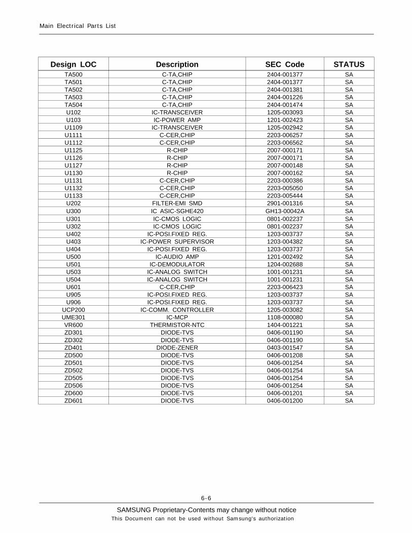
Main Electrical Parts List
6-6
This Document can not be used without Samsung's authorization
Design LOC Description SEC Code STATUSTA500 C-TA,CHIP 2404-001377 SATA501 C-TA,CHIP 2404-001377 SATA502 C-TA,CHIP 2404-001381 SATA503 C-TA,CHIP 2404-001226 SATA504 C-TA,CHIP 2404-001474 SAU102 IC-TRANSCEIVER 1205-003093 SAU103 IC-POWER AMP 1201-002423 SAU1109 IC-TRANSCEIVER 1205-002942 SAU1111 C-CER,CHIP 2203-006257 SAU1112 C-CER,CHIP 2203-006562 SAU1125 R-CHIP 2007-000171 SAU1126 R-CHIP 2007-000171 SAU1127 R-CHIP 2007-000148 SAU1130 R-CHIP 2007-000162 SAU1131 C-CER,CHIP 2203-000386 SAU1132 C-CER,CHIP 2203-005050 SAU1133 C-CER,CHIP 2203-005444 SAU202 FILTER-EMI SMD 2901-001316 SAU300 IC ASIC-SGHE420 GH13-00042A SAU301 IC-CMOS LOGIC 0801-002237 SAU302 IC-CMOS LOGIC 0801-002237 SAU402 IC-POSI.FIXED REG. 1203-003737 SAU403 IC-POWER SUPERVISOR 1203-004382 SAU404 IC-POSI.FIXED REG. 1203-003737 SAU500 IC-AUDIO AMP 1201-002492 SAU501 IC-DEMODULATOR 1204-002688 SAU503 IC-ANALOG SWITCH 1001-001231 SAU504 IC-ANALOG SWITCH 1001-001231 SAU601 C-CER,CHIP 2203-006423 SAU905 IC-POSI.FIXED REG. 1203-003737 SAU906 IC-POSI.FIXED REG. 1203-003737 SA
UCP200 IC-COMM. CONTROLLER 1205-003082 SAUME301 IC-MCP 1108-000080 SAVR600 THERMISTOR-NTC 1404-001221 SAZD301 DIODE-TVS 0406-001190 SAZD302 DIODE-TVS 0406-001190 SAZD401 DIODE-ZENER 0403-001547 SAZD500 DIODE-TVS 0406-001208 SAZD501 DIODE-TVS 0406-001254 SAZD502 DIODE-TVS 0406-001254 SAZD505 DIODE-TVS 0406-001254 SAZD506 DIODE-TVS 0406-001254 SAZD600 DIODE-TVS 0406-001201 SAZD601 DIODE-TVS 0406-001200 SA
SAMSUNG Proprietary-Contents may change without noticeThis Document can not be used without Samsung's authorization
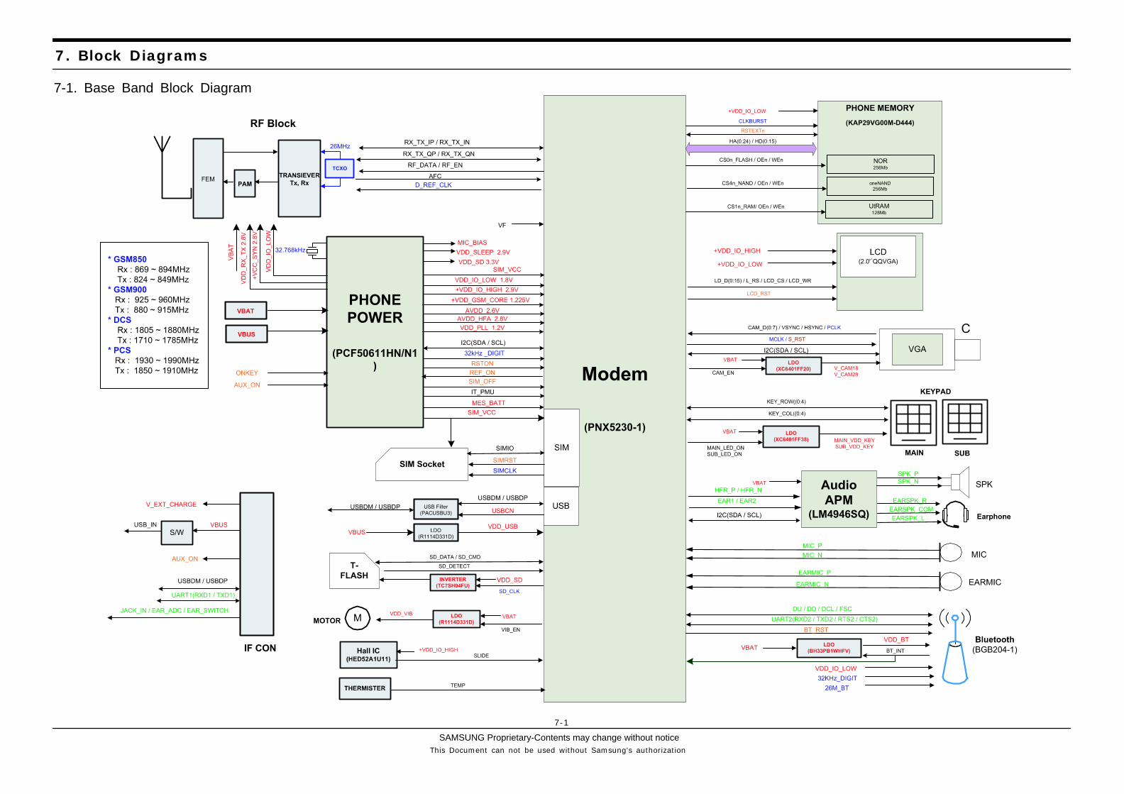
7. Block Diagrams
7-1
7-1. Base Band Block Diagram
SAMSUNG Proprietary-Contents may change without notice
Block Diagrams
7-2
This Document can not be used without Samsung's authorization
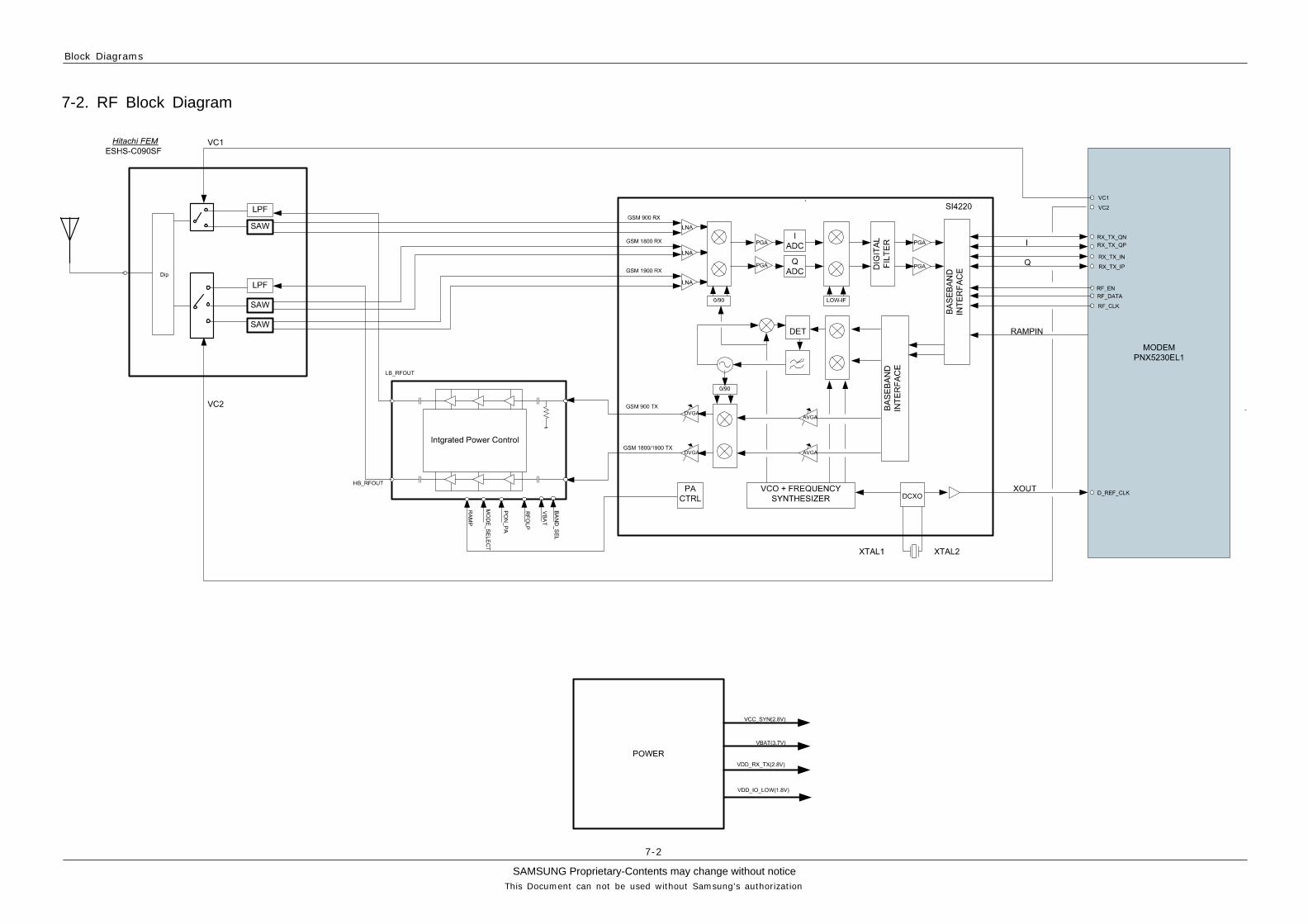
7-2. RF Block Diagram
SAMSUNG Proprietary-Contents may change without notice
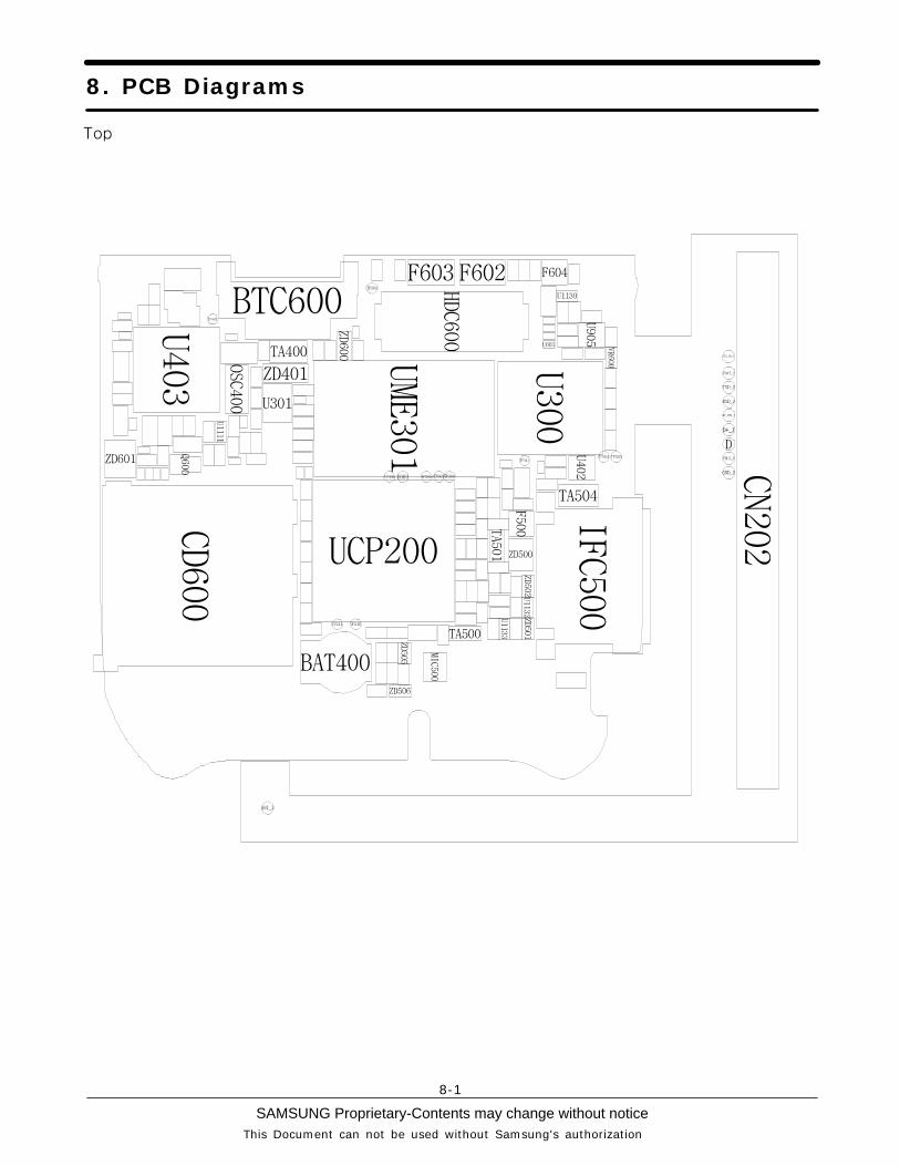
8. PCB Diagrams
8-1
This Document can not be used without Samsung's authorization
Top
SAMSUNG Proprietary-Contents may change without notice
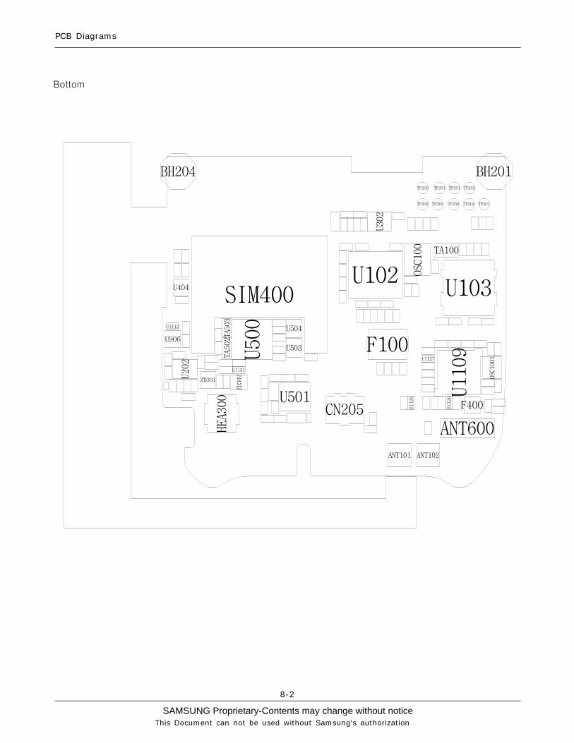
PCB Diagrams
8-2
This Document can not be used without Samsung's authorization
Bottom
SAMSUNG Proprietary-Contents may change without notice
9. Flow Chart of Troubleshooting
This Document can not be used without Samsung's authorization
9-1
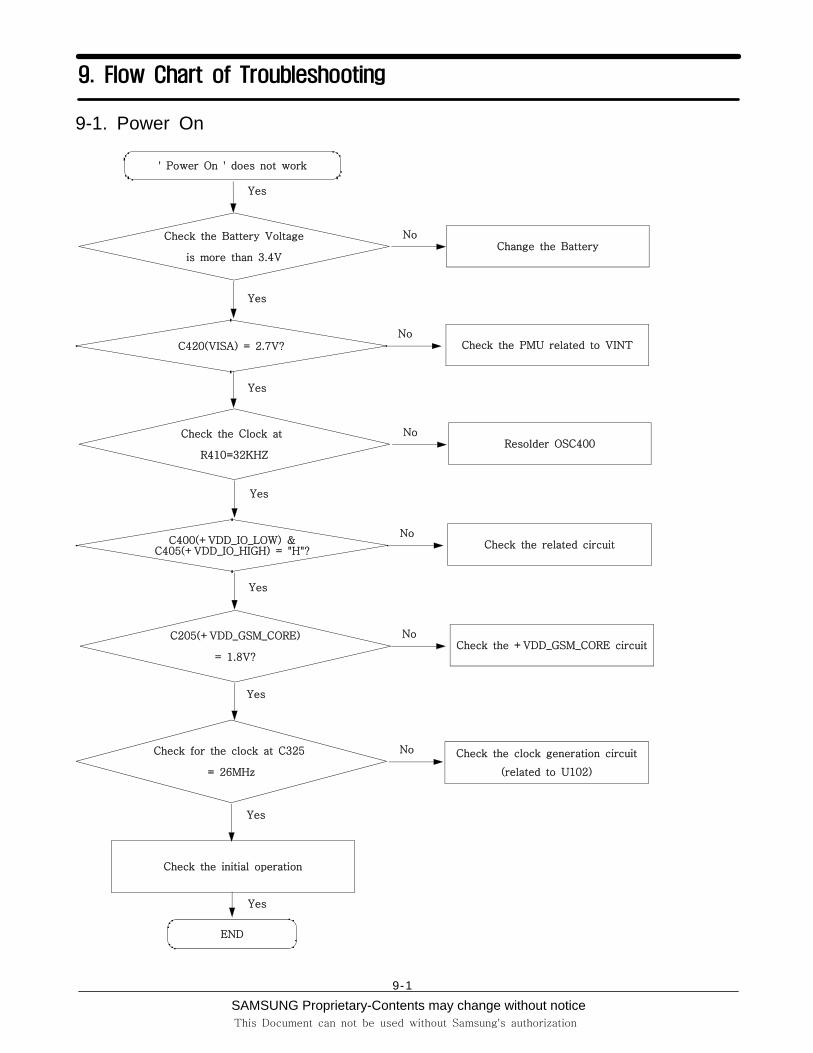
9-1. Power On
Check the Battery Voltage
is more than 3.4V
' Power On ' does not work
Change the Battery
END
No
Yes
C420(VISA) = 2.7V? Check the PMU related to VINTNo
Yes
Check the Clock at
R410=32KHZResolder OSC400
No
Yes
C400(+VDD_IO_LOW) &C405(+VDD_IO_HIGH) = "H"?
Check the related circuitNo
Yes
C205(+VDD_GSM_CORE)
= 1.8V?Check the +VDD_GSM_CORE circuit
No
Yes
Check for the clock at C325
= 26MHz
Check the clock generation circuit
(related to U102)
No
Yes
Check the initial operation
Yes
Yes

SAMSUNG Proprietary-Contents may change without noticeThis Document can not be used without Samsung's authorization
Flow Chart of Troubleshooting
9-2
SAMSUNG Proprietary-Contents may change without notice
Flow Chart of Troubleshooting
This Document can not be used without Samsung's authorization
9-3
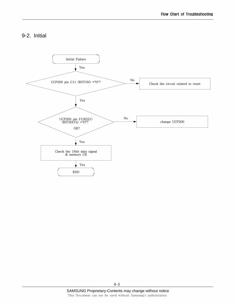
9-2. Initial
UCP200 pin C11 (RSTON) ="H"?
Initial Failure
Check the circuit related to reset
END
No
Yes
UCP200 pin F1(R221)(RSTEXTn) ="H"?
OK?
Yes
Yes
Nochange UCP200
Check the 16bit data signal& memory CE
Yes
SAMSUNG Proprietary-Contents may change without noticeThis Document can not be used without Samsung's authorization
Flow Chart of Troubleshooting
9-4
SAMSUNG Proprietary-Contents may change without notice
Flow Chart of Troubleshooting
This Document can not be used without Samsung's authorization
9-5
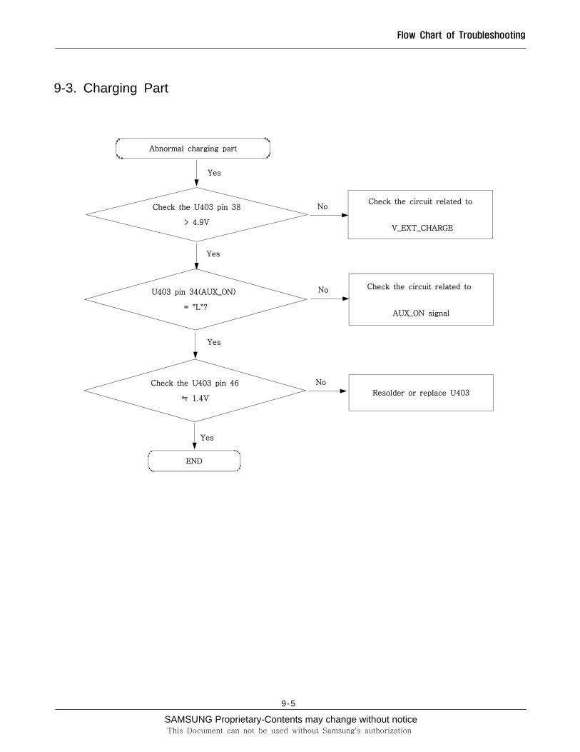
9-3. Charging Part
Check the U403 pin 38
> 4.9V
Abnormal charging part
END
No
Yes
U403 pin 34(AUX_ON)
= "L"?
No
Yes
Check the U403 pin 46
≒ 1.4V
No
Yes
Check the circuit related to
V_EXT_CHARGE
Check the circuit related to
AUX_ON signal
Resolder or replace U403
Yes

SAMSUNG Proprietary-Contents may change without noticeThis Document can not be used without Samsung's authorization
Flow Chart of Troubleshooting
9-6

SAMSUNG Proprietary-Contents may change without notice
Flow Chart of Troubleshooting
This Document can not be used without Samsung's authorization
9-7
9-4. Sim Part
SIM400 pin 1,5 = "H"?
Phone can't access SIM Card
Resolder or replace U403
Check the SIM Card
END
No
Yes
Yes
Yes
No
Check the Clock
After Power ON,
Check SIMCLK Signal on
pin3 of SIM400 in a few second
Yes
No
Replace PBAAfter SIM card insert,
SIM400 pin 2 = "H(SIM_RST)"?
Yes
SAMSUNG Proprietary-Contents may change without noticeThis Document can not be used without Samsung's authorization
Flow Chart of Troubleshooting
9-8

SAMSUNG Proprietary-Contents may change without notice
Flow Chart of Troubleshooting
This Document can not be used without Samsung's authorization
9-9
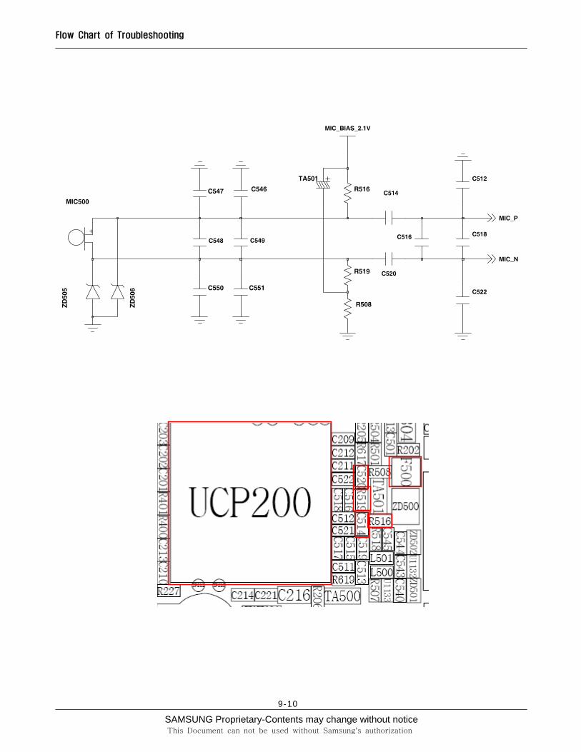
9-5. Microphone Part
Check the connection
from MIC
Check the circuit
from UCP200 to MIC
Resolder MIC
Resolder the C514, C520, R516, R519
END
No
Yes
Yes
Yes
Yes
No
Check F500 PIN 8= ' H' ?
NoCheck the JACK_IN signal
Microphone does not work
Yes
Check the MICNo
Replace the MIC
SAMSUNG Proprietary-Contents may change without noticeThis Document can not be used without Samsung's authorization
Flow Chart of Troubleshooting
9-10
SAMSUNG Proprietary-Contents may change without notice
Flow Chart of Troubleshooting
This Document can not be used without Samsung's authorization
9-11
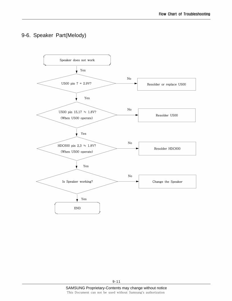
9-6. Speaker Part(Melody)
U500 pin 7 = 2.9V?
Speaker does not work
U500 pin 15,17 ≒ 1.8V?
(When U500 operate)Resolder U500
No
Yes
No
Resolder or replace U500
Yes
HDC600 pin 2,3 ≒ 1.8V?
(When U500 operate)Resolder HDC600
No
Yes
END
Yes
Is Speaker working? Change the Speaker
No
Yes

SAMSUNG Proprietary-Contents may change without noticeThis Document can not be used without Samsung's authorization
Flow Chart of Troubleshooting
9-12
SAMSUNG Proprietary-Contents may change without notice
Flow Chart of Troubleshooting
This Document can not be used without Samsung's authorization
9-13
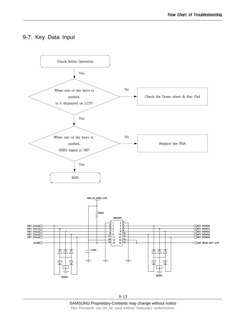
9-7. Key Data Input
When one of the keys is
pushed,
is it displayed on LCD?
Check the Dome sheet & Key Pad
END
No
Yes
Yes
Check Initial Operation
When one of the keys is
pushed,
KBIO signal is OK?
Replace the PBA
No
Yes
SAMSUNG Proprietary-Contents may change without noticeThis Document can not be used without Samsung's authorization
Flow Chart of Troubleshooting
9-14
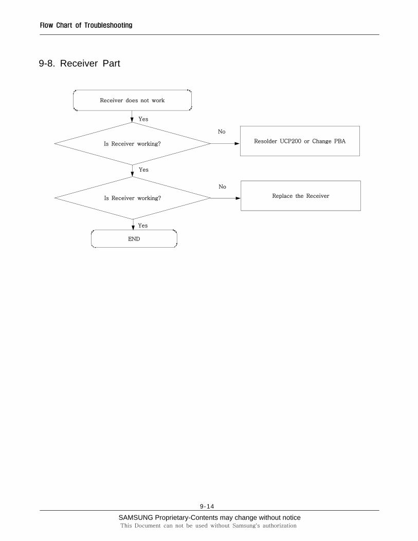
9-8. Receiver Part
Is Receiver working? Resolder UCP200 or Change PBA
END
No
Yes
Yes
Receiver does not work
No
Replace the Receiver
Yes
Is Receiver working?

SAMSUNG Proprietary-Contents may change without notice
Flow Chart of Troubleshooting
This Document can not be used without Samsung's authorization
9-15
9-9. Back Light (for Color Main LCD)
Is LCD Contrast set on high
level in the Menu?
Set LCD Contrast on high level
END
No
Yes
Yes
Backlight does not work
HDC600 PIN 21 = H ? Resolder HDC600 or change PBA
No
Yes
SAMSUNG Proprietary-Contents may change without noticeThis Document can not be used without Samsung's authorization
Flow Chart of Troubleshooting
9-16
SAMSUNG Proprietary-Contents may change without notice
Flow Chart of Troubleshooting
This Document can not be used without Samsung's authorization
9-17
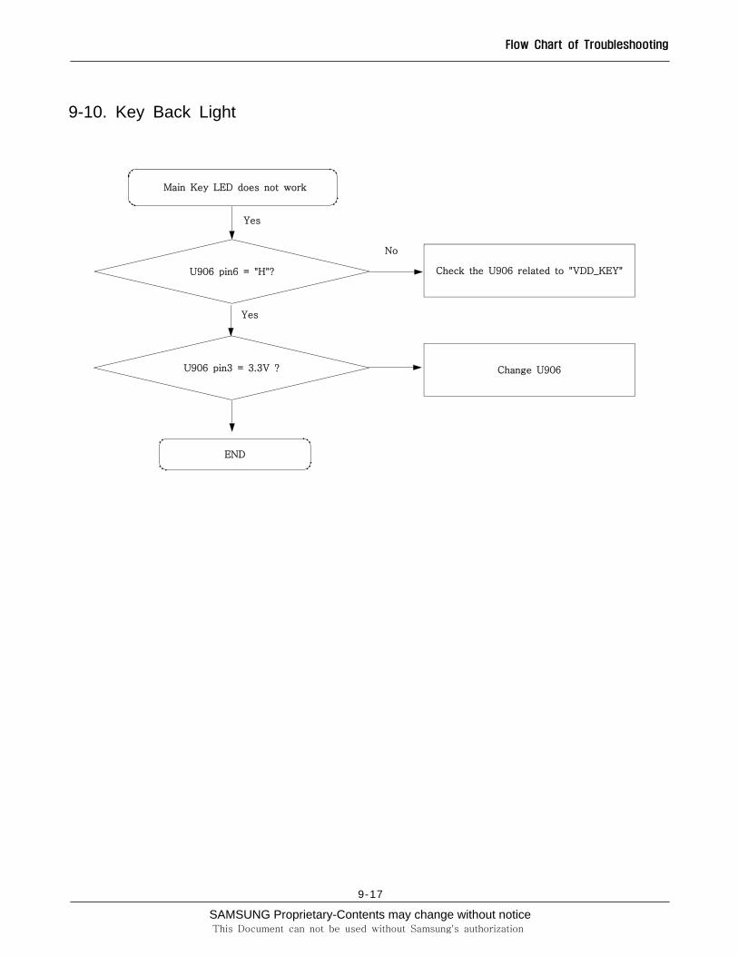
9-10. Key Back Light
U906 pin6 = "H"? Check the U906 related to "VDD_KEY"
END
No
Yes
Yes
Main Key LED does not work
U906 pin3 = 3.3V ? Change U906
SAMSUNG Proprietary-Contents may change without noticeThis Document can not be used without Samsung's authorization
Flow Chart of Troubleshooting
9-18
SAMSUNG Proprietary-Contents may change without notice
Flow Chart of Troubleshooting
This Document can not be used without Samsung's authorization
9-19
9-11. Camera part
"Camera" function does not work
Yes
No
Reconnect the camera moduleCheck the Camera
connector on LCD module
Yes
HDC600 Pin21 = H?
No
Resolder HDC600 or change PBA
Yes
C310 = 26MHz
NoCheck U102(pin8) related to
26MHz and C131
Yes
Is there another problem?
END
Replace the cameramodule
Yes
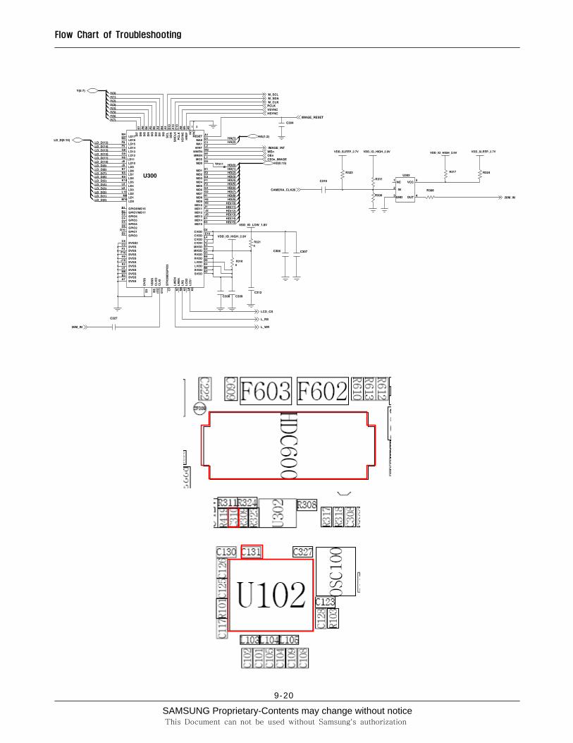
SAMSUNG Proprietary-Contents may change without noticeThis Document can not be used without Samsung's authorization
Flow Chart of Troubleshooting
9-20

SAMSUNG Proprietary-Contents may change without notice
Flow Chart of Troubleshooting
This Document can not be used without Samsung's authorization
9-21
9-12. GSM Receiver
Check ANT Switchcontrol circuit
Resolder F100
Check & ResolderC117,L123,C126And PMU Part
Resolder U102
RX ONRF input : CH center freq : +67.7kHz
Cell Power : -60dBm
Yes
F100 Pin13≥ -65dBm
NoResolder CN205,C103,L102
Yes
F100 1,2≥ -68dBm
Check F100pin9,pin11 = L
NoNo
Yes
Yes
No
Resolder C108, C109, L105U101
pin 24 ≥ -70dBmpin 25 ≥ -70dBm
Yes
NoU101pin 16,17,2932,36 ≥2.8Vpin10≥1.8V
U101 pin 4,5,6,7≥ 0.2Vp_p
No
YesYes
Check UCP200
END
SAMSUNG Proprietary-Contents may change without noticeThis Document can not be used without Samsung's authorization
Flow Chart of Troubleshooting
9-22
9-13. GSM Transmitter
U101pin 16,17,2932,36 ≥2.8Vpin10≥1.8V
NoResolder U102
Check UCP200
END
No
Yes
No
Yes
Yes
Yes
Yes
Yes
Yes
No
Yes
No
No
No
No
Check U102,C117,C126,L123
Check VBAT or PAMcontrol signal
Resolder or Change U103Check U103pin 2,3,5,6,8+Vbatt pin4,
OK?
Yes
U102 pin 4,5,6,7≥ 0.2Vp_p
Resolder or Change L101,
Check ANT Switchcontrol circuit
Change or Resolder F100
U103 pin7≥ -4dBm
U103 pin12≥ 30dBm
F100 pin10≥ 30dBm
Check F100pin11 = H (2.6V),
Pin9 = L
TX ON (5Level)
Resolder CN205,C103,L102F100 Pin13≥ 30dBm

SAMSUNG Proprietary-Contents may change without notice
Flow Chart of Troubleshooting
This Document can not be used without Samsung's authorization
9-23
9-14. DCS Receiver
Check F100pin9,pin11 = L
Check UCP201
No
NoNo
No
No
Yes
YesYes
Yes
Yes
Yes
Resolder U102
Check & ResolderU102, C117,C123,C126
And PMU Part
U101 pin16,17,29,32,36 ≥2.8Vpin 10≥1.8V
Resolder C104, C105, L104
Resolder F100
Check ANT Switchcontrol circuit
U102pin 22 ≥ -70dBmpin 23 ≥ -70dBm
U101 pin 4,5,6,7≥ 0.2Vp_p
F100 3,4≥ -68dBm
RX ONRF input : CH center freq : +67.7kHz
Cell Power : -60dBm
Yes
No
END
Resolder CN205,C103,L102F100 Pin13≥ -65dBm
SAMSUNG Proprietary-Contents may change without noticeThis Document can not be used without Samsung's authorization
Flow Chart of Troubleshooting
9-24
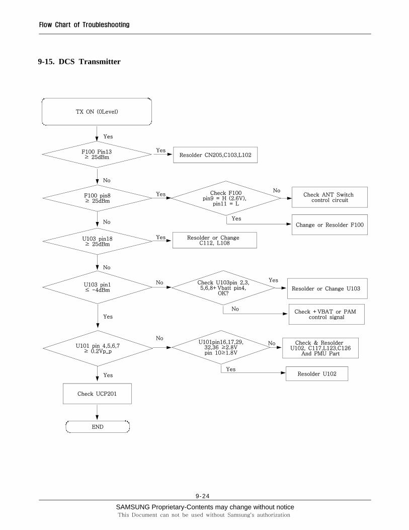
9-15. DCS Transmitter
U101pin16,17,29,32,36 ≥2.8Vpin 10≥1.8V
Yes Resolder U102
Check UCP201
END
No
Yes
No
No
No
Yes
Yes
Yes
Yes
No
Yes
Yes
No
No
No
Check & ResolderU102, C117,L123,C126
And PMU Part
Check +VBAT or PAMcontrol signal
Resolder or Change U103Check U103pin 2,3,5,6,8+Vbatt pin4,
OK?
Yes
U101 pin 4,5,6,7≥ 0.2Vp_p
Resolder or ChangeC112, L108
Check ANT Switchcontrol circuit
Change or Resolder F100
U103 pin1≤ -4dBm
U103 pin18≥ 25dBm
F100 pin8≥ 25dBm
Check F100pin9 = H (2.6V),pin11 = L
TX ON (0Level)
Resolder CN205,C103,L102F100 Pin13≥ 25dBm
SAMSUNG Proprietary-Contents may change without notice
Flow Chart of Troubleshooting
This Document can not be used without Samsung's authorization
9-25
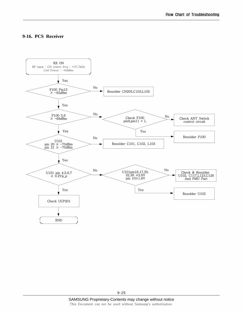
9-16. PCS Receiver
RX ONRF input : CH center freq : +67.7kHz
Cell Power : -60dBm
Yes
F100 Pin13≥ -65dBm
NoResolder CN205,C103,L102
Yes
F100 5,6≥ -68dBm Check F100
pin9,pin11 = L
NoNo
Check ANT Switchcontrol circuit
YesYes
Resolder F100
U101pin 20 ≥ -70dBmpin 21 ≥ -70dBm
No
Resolder C101, C102, L103
Yes
U101pin16,17,29,32,36 ≥2.8Vpin 10≥1.8V
U101 pin 4,5,6,7≥ 0.2Vp_p
NoNoCheck & ResolderU102, C117,L123,C126
And PMU Part
YesYesResolder U102
Check UCP201
END
SAMSUNG Proprietary-Contents may change without noticeThis Document can not be used without Samsung's authorization
Flow Chart of Troubleshooting
9-26
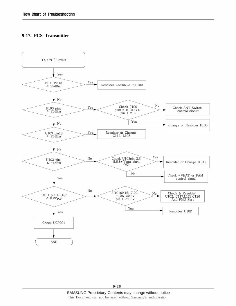
9-17. PCS Transmitter
U101pin16,17,29,32,36 ≥2.8Vpin 10≥1.8V
Yes Resolder U102
Check UCP201
END
No
Yes
No
No
No
Yes
Yes
Yes
Yes
No
Yes
Yes
No
No
No
Check & ResolderU102, C117,L123,C126
And PMU Part
Check +VBAT or PAMcontrol signal
Resolder or Change U103Check U103pin 2,3,5,6,8+Vbatt pin4,
OK?
Yes
U101 pin 4,5,6,7≥ 0.2Vp_p
Resolder or ChangeC112, L108
Check ANT Switchcontrol circuit
Change or Resolder F100
U103 pin1≤ -4dBm
U103 pin18≥ 25dBm
F100 pin8≥ 25dBm
Check F100pin9 = H (2.6V),pin11 = L
TX ON (0Level)
Resolder CN205,C103,L102F100 Pin13≥ 25dBm
SAMSUNG Proprietary-Contents may change without notice
Flow Chart of Troubleshooting
This Document can not be used without Samsung's authorization
9-27
SAMSUNG Proprietary-Contents may change without noticeThis Document can not be used without Samsung's authorization
Flow Chart of Troubleshooting
9-28
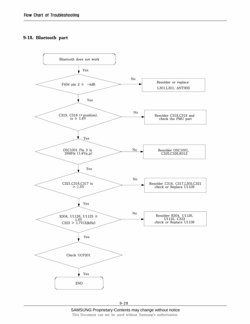
9-18. Bluetooth part
F404 pin 2 ≥ -4dB
Bluetooth does not work
C319, C318 (+position),is ≥ 1.8V
Resolder C318,C319 andcheck the PMU part
No
Yes
No
Resolder or replace
L301,L301, ANT900
Yes
OSC1001 Pin 3 is26MHz (1.4Vp_p)
Resolder OSC1001,C325,C326,R312
No
Yes
No
END
R304, U1126, U1125 ≥1.8V
C323 ≥ 1.7V(32kHz)
Resolder R304, U1126,U1125, C323
check or Replace U1109
Yes
Yes
C321,C316,C317 is≥ 1.5V
Resolder C316, C317,L303,C321check or Replace U1109
No
Yes
Check UCP201
Yes
SAMSUNG Proprietary-Contents may change without notice
Flow Chart of Troubleshooting
This Document can not be used without Samsung's authorization
9-29
SAMSUNG Proprietary-Contents may change without noticeThis Document can not be used without Samsung's authorization
Flow Chart of Troubleshooting
9-30
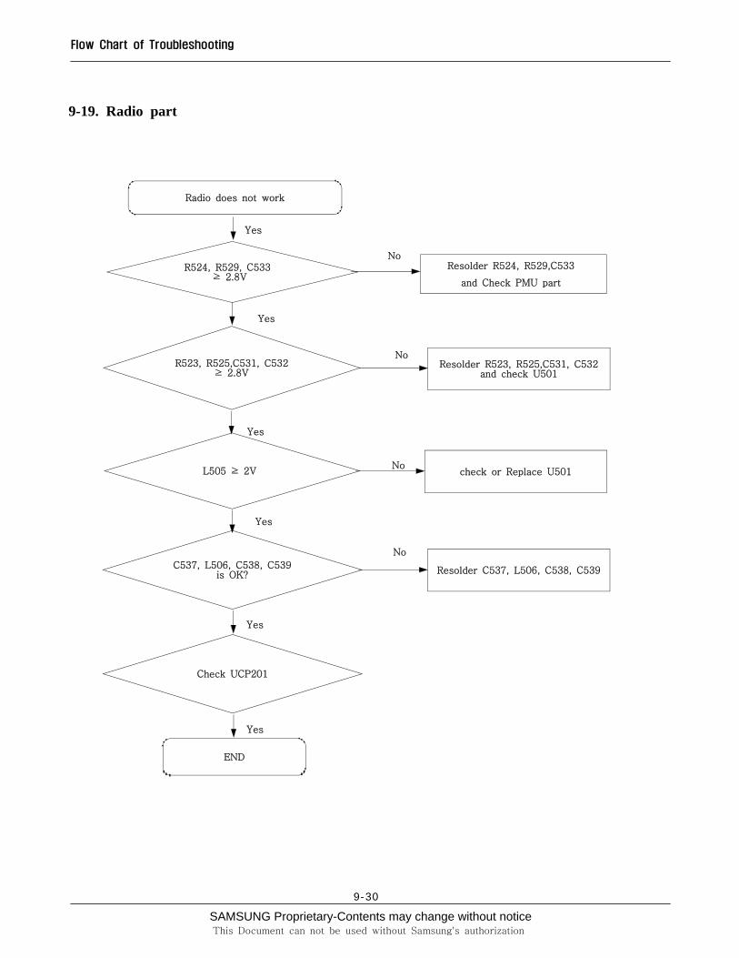
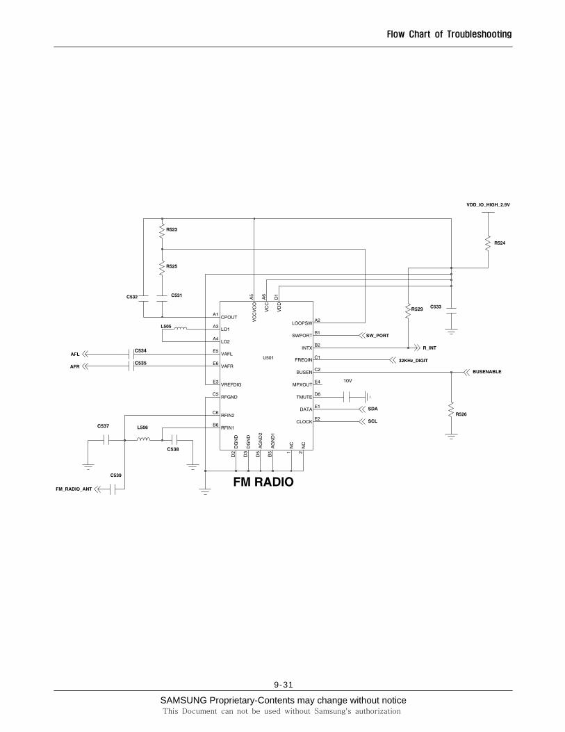
9-19. Radio part
R524, R529, C533≥ 2.8V
Radio does not work
R523, R525,C531, C532≥ 2.8V
Resolder R523, R525,C531, C532and check U501
No
Yes
No
Resolder R524, R529,C533
and Check PMU part
Yes
L505 ≥ 2V check or Replace U501No
Yes
END
Yes
C537, L506, C538, C539is OK? Resolder C537, L506, C538, C539
No
Yes
Check UCP201
Yes
SAMSUNG Proprietary-Contents may change without notice
Flow Chart of Troubleshooting
This Document can not be used without Samsung's authorization
9-31
SAMSUNG Proprietary-Contents may change without noticeThis Document can not be used without Samsung's authorization
Flow Chart of Troubleshooting
9-32

SAMSUNG Proprietary-Contents may change without notice
10. Reference data
10-1
This Document can not be used without Samsung's authorization
Reference Abbreviate
― AAC: Advanced Audio Coding.― AVC : Advanced Video Coding.― BER : Bit Error Rate― BPSK: Binary Phase Shift Keying― CA : Conditional Access― CDM : Code Division Multiplexing― C/I : Carrier to Interference― DMB : Digital Multimedia Broadcasting― EN : European Standard― ES : Elementary Stream― ETSI: European Telecommunications Standards Institute― MPEG: Moving Picture Experts Group― PN : Pseudo-random Noise― PS : Pilot Symbol― QPSK: Quadrature Phase Shift Keying― RS : Reed-Solomon― SI : Service Information― TDM : Time Division Multiplexing― TS : Transport Stream

SAMSUNG Proprietary-Contents may change without notice
Reference data
10-2
This Document can not be used without Samsung's authorization
Samsung Electronics Co.,Ltd.
2006. 12. Rev.1.0
ⓒThis Service Manual is a property of Samsung Electronics Co.,Ltd.Any unauthorized use of Manual can be punished under applicableInternational and/or domestic law.