sgm8198 high-side measurement current shunt monitor
TRANSCRIPT
SGM8198
High-side Measurement Current Shunt Monitor
SG Micro Corp www.sg-micro.com
JANUARY 2021 – REV. A. 2
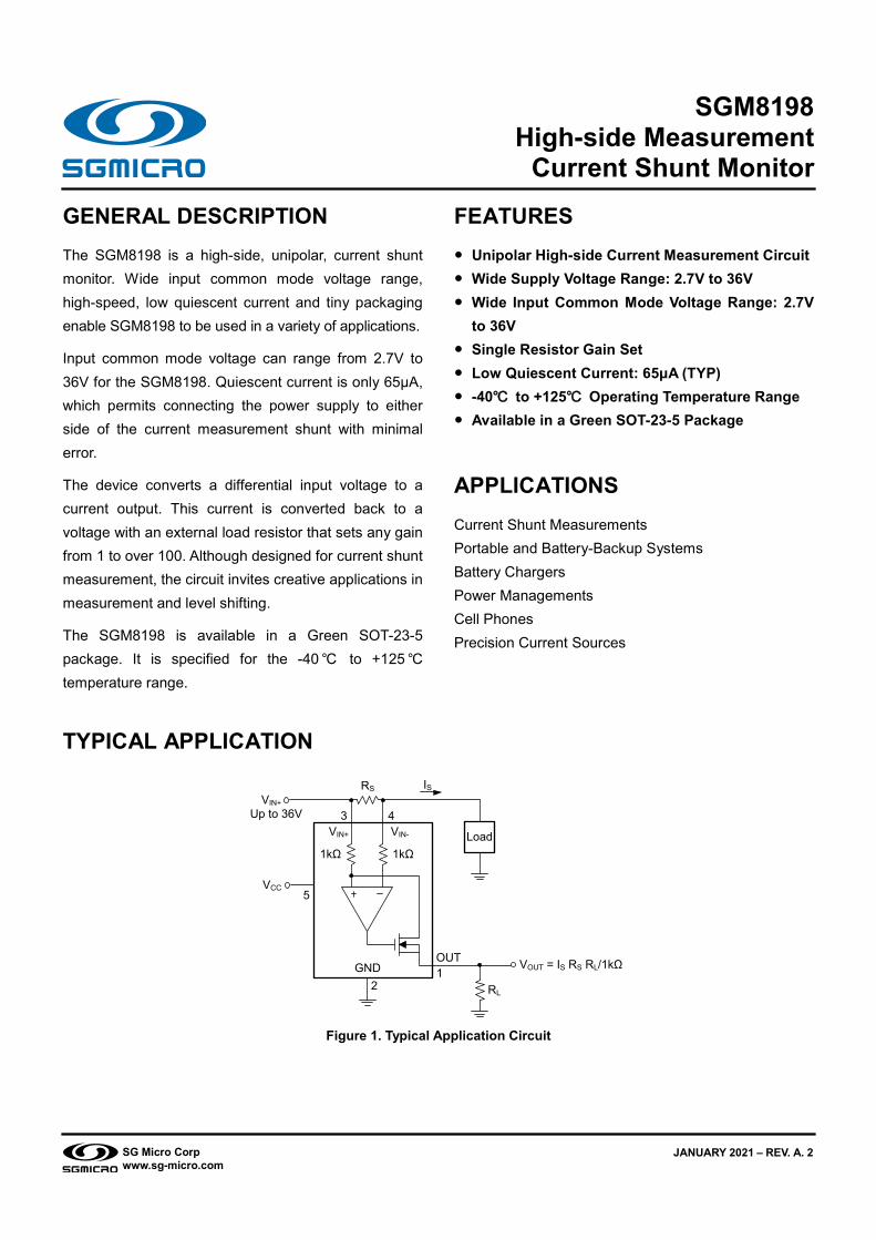
GENERAL DESCRIPTION The SGM8198 is a high-side, unipolar, current shunt monitor. Wide input common mode voltage range, high-speed, low quiescent current and tiny packaging enable SGM8198 to be used in a variety of applications.
Input common mode voltage can range from 2.7V to 36V for the SGM8198. Quiescent current is only 65µA, which permits connecting the power supply to either side of the current measurement shunt with minimal error.
The device converts a differential input voltage to a current output. This current is converted back to a voltage with an external load resistor that sets any gain from 1 to over 100. Although designed for current shunt measurement, the circuit invites creative applications in measurement and level shifting.
The SGM8198 is available in a Green SOT-23-5 package. It is specified for the -40 to +125 temperature range.
FEATURES Unipolar High-side Current Measurement Circuit Wide Supply Voltage Range: 2.7V to 36V Wide Input Common Mode Voltage Range: 2.7V
to 36V Single Resistor Gain Set Low Quiescent Current: 65μA (TYP) -40 to +125 Operating Temperature Range Available in a Green SOT-23-5 Package
APPLICATIONS Current Shunt Measurements Portable and Battery-Backup Systems Battery Chargers Power Managements Cell Phones Precision Current Sources
TYPICAL APPLICATION
VIN+
VIN+ VIN-
GND
VCC
Up to 36V
RS IS
OUT
RL
Load
VOUT = IS RS RL/1kΩ
1kΩ 1kΩ
12
3 4
5
Figure 1. Typical Application Circuit

High-side Measurement SGM8198 Current Shunt Monitor
2 JANUARY 2021 SG Micro Corp
www.sg-micro.com
PACKAGE/ORDERING INFORMATION
MODEL PACKAGE DESCRIPTION
SPECIFIED TEMPERATURE
RANGE ORDERING NUMBER
PACKAGE MARKING
PACKING OPTION
SGM8198 SOT-23-5 -40 to +125 SGM8198XN5G/TR GMCXX Tape and Reel, 3000
MARKING INFORMATION NOTE: XX = Date Code.
Date Code - Year Date Code - Week
Serial Number
YYY X X
Green (RoHS & HSF): SG Micro Corp defines "Green" to mean Pb-Free (RoHS compatible) and free of halogen substances. If you have additional comments or questions, please contact your SGMICRO representative directly.
ABSOLUTE MAXIMUM RATINGS Supply Voltage Range ....................................... -0.3V to 40V Analog Inputs (VIN+, VIN-) Common Mode Voltage Range
........................................................................... -0.3V to 40V Analog Output Voltage Range, VOUT .................. -0.3V to 40V Input Current into Any Pin ............................................. 10mA Package Thermal Resistance SOT-23-5, θJA .......................................................... 199/W Junction Temperature ................................................. +150 Storage Temperature Range ....................... -65 to +150 Lead Temperature (Soldering, 10s) ............................ +260 ESD Susceptibility HBM ............................................................................. 2000V CDM ............................................................................. 1000V RECOMMENDED OPERATING CONDITIONS Operating Voltage Range ..................................... 2.7V to 36V Operating Temperature Range .................... -40 to +125 OVERSTRESS CAUTION Stresses beyond those listed in Absolute Maximum Ratings may cause permanent damage to the device. Exposure to absolute maximum rating conditions for extended periods may affect reliability. Functional operation of the device at any conditions beyond those indicated in the Recommended Operating Conditions section is not implied.
ESD SENSITIVITY CAUTION This integrated circuit can be damaged if ESD protections are not considered carefully. SGMICRO recommends that all integrated circuits be handled with appropriate precautions. Failure to observe proper handling and installation procedures can cause damage. ESD damage can range from subtle performance degradation to complete device failure. Precision integrated circuits may be more susceptible to damage because even small parametric changes could cause the device not to meet the published specifications. DISCLAIMER SG Micro Corp reserves the right to make any change in circuit design, or specifications without prior notice.
PIN CONFIGURATION (TOP VIEW)
SOT-23-5
VCC
VIN-3 4
51
2GND
VIN+
OUT
High-side Measurement SGM8198 Current Shunt Monitor
3 JANUARY 2021 SG Micro Corp
www.sg-micro.com
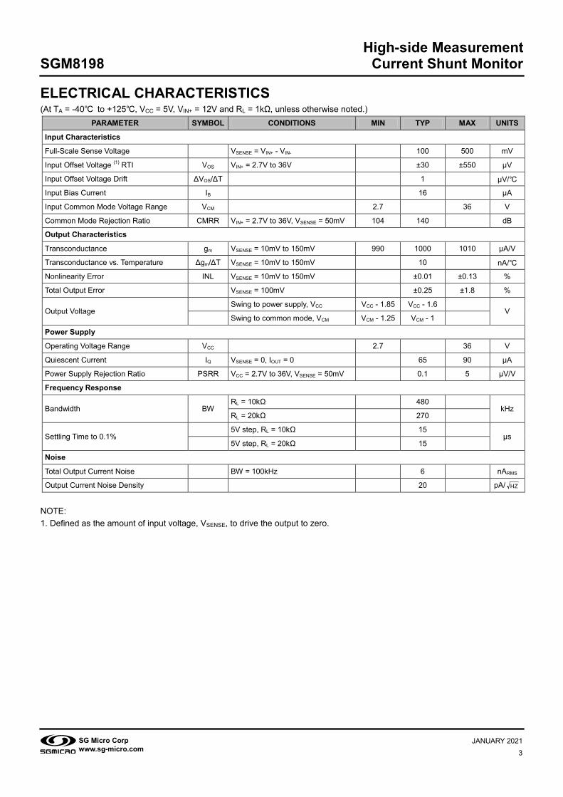
ELECTRICAL CHARACTERISTICS (At TA = -40 to +125, VCC = 5V, VIN+ = 12V and RL = 1kΩ, unless otherwise noted.)
PARAMETER SYMBOL CONDITIONS MIN TYP MAX UNITS
Input Characteristics
Full-Scale Sense Voltage VSENSE = VIN+ - VIN- 100 500 mV
Input Offset Voltage (1) RTI VOS VIN+ = 2.7V to 36V ±30 ±550 μV
Input Offset Voltage Drift ΔVOS/ΔT 1 μV/
Input Bias Current IB 16 μA
Input Common Mode Voltage Range VCM 2.7 36 V
Common Mode Rejection Ratio CMRR VIN+ = 2.7V to 36V, VSENSE = 50mV 104 140 dB
Output Characteristics
Transconductance gm VSENSE = 10mV to 150mV 990 1000 1010 μA/V
Transconductance vs. Temperature Δgm/ΔT VSENSE = 10mV to 150mV 10 nA/
Nonlinearity Error INL VSENSE = 10mV to 150mV ±0.01 ±0.13 %
Total Output Error VSENSE = 100mV ±0.25 ±1.8 %
Output Voltage Swing to power supply, VCC VCC - 1.85 VCC - 1.6
V Swing to common mode, VCM VCM - 1.25 VCM - 1
Power Supply
Operating Voltage Range VCC 2.7 36 V
Quiescent Current IQ VSENSE = 0, IOUT = 0 65 90 μA
Power Supply Rejection Ratio PSRR VCC = 2.7V to 36V, VSENSE = 50mV 0.1 5 μV/V
Frequency Response
Bandwidth BW RL = 10kΩ 480
kHz RL = 20kΩ 270
Settling Time to 0.1% 5V step, RL = 10kΩ 15
μs 5V step, RL = 20kΩ 15
Noise
Total Output Current Noise BW = 100kHz 6 nARMS
Output Current Noise Density 20 pA/ HZ
NOTE: 1. Defined as the amount of input voltage, VSENSE, to drive the output to zero.

High-side Measurement SGM8198 Current Shunt Monitor
4 JANUARY 2021 SG Micro Corp
www.sg-micro.com
TYPICAL PERFORMANCE CHARACTERISTICS At TA = +25, VCC = 5V, VIN+ = 12V and RL = 1kΩ, unless otherwise noted.
Total Output Error vs. Supply Voltage Quiescent Current vs. Supply Voltage
Total Output Error vs. Input Voltage Gain vs. Frequency
CMRR vs. Frequency PSRR vs. Frequency
-1.5
-1
-0.5
0
0.5
1
0 5 10 15 20 25 30 35 40
Tota
l Out
put E
rror (
%)
Supply Voltage (V)
— G = 1 — G = 10 — G = 25
10
20
30
40
50
60
70
80
0 5 10 15 20 25 30 35 40
Qui
esce
nt C
urre
nt (μ
A)
Supply Voltage (V)
— -55 — -40 — +25 — +125 — +150
-1
-0.5
0
0.5
1
1.5
0 25 50 75 100 125 150 175 200
Tota
l Out
put E
rror (
%)
Input Voltage (mV)
— -40 — +25 — +125
-40
-20
0
20
40
60
0.1 1 10 100 1000 10000
Gai
n (d
B)
Frequency (kHz)
RL = 1kΩ
RL = 10kΩ
RL = 100kΩ
-140
-120
-100
-80
-60
-40
-20
0
0.01 0.1 1 10 100 1000
Com
mon
Mod
e R
ejec
tion
Rat
io (d
B)
Frequency (kHz)
— G= 1 — G= 10 — G = 100
-150
-120
-90
-60
-30
0
0.01 0.1 1 10 100 1000 10000
Pow
er S
uppl
y R
ejec
tion
Rat
io (d
B)
Frequency (kHz)
— G = 1 — G = 10 — G = 100

High-side Measurement SGM8198 Current Shunt Monitor
5 JANUARY 2021 SG Micro Corp
www.sg-micro.com
TYPICAL PERFORMANCE CHARACTERISTICS (continued) At TA = +25, VCC = 5V, VIN+ = 12V and RL = 1kΩ, unless otherwise noted.
Step Response Step Response
1.5V
0.5V
1V
0V
Time (20μs/div) Time (10μs/div)
Step Response Step Response
1V
0V
2V
0V
Time (20μs/div) Time (10μs/div)
G = 100 G = 50
G = 100 G = 10
High-side Measurement SGM8198 Current Shunt Monitor
6 JANUARY 2021 SG Micro Corp
www.sg-micro.com
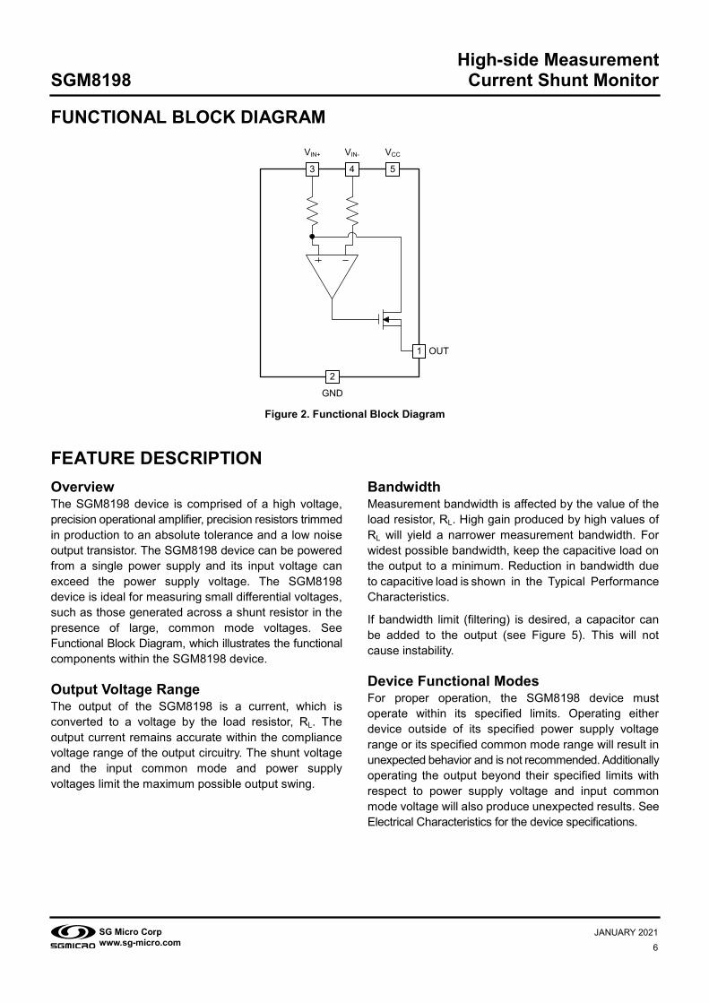
FUNCTIONAL BLOCK DIAGRAM
Figure 2. Functional Block Diagram
FEATURE DESCRIPTION Overview The SGM8198 device is comprised of a high voltage, precision operational amplifier, precision resistors trimmed in production to an absolute tolerance and a low noise output transistor. The SGM8198 device can be powered from a single power supply and its input voltage can exceed the power supply voltage. The SGM8198 device is ideal for measuring small differential voltages, such as those generated across a shunt resistor in the presence of large, common mode voltages. See Functional Block Diagram, which illustrates the functional components within the SGM8198 device. Output Voltage Range The output of the SGM8198 is a current, which is converted to a voltage by the load resistor, RL. The output current remains accurate within the compliance voltage range of the output circuitry. The shunt voltage and the input common mode and power supply voltages limit the maximum possible output swing.
Bandwidth Measurement bandwidth is affected by the value of the load resistor, RL. High gain produced by high values of RL will yield a narrower measurement bandwidth. For widest possible bandwidth, keep the capacitive load on the output to a minimum. Reduction in bandwidth due to capacitive load is shown in the Typical Performance Characteristics.
If bandwidth limit (filtering) is desired, a capacitor can be added to the output (see Figure 5). This will not cause instability. Device Functional Modes For proper operation, the SGM8198 device must operate within its specified limits. Operating either device outside of its specified power supply voltage range or its specified common mode range will result in unexpected behavior and is not recommended. Additionally operating the output beyond their specified limits with respect to power supply voltage and input common mode voltage will also produce unexpected results. See Electrical Characteristics for the device specifications.
VIN+ VIN-
GND
VCC
OUT
2
1
3 4 5

High-side Measurement SGM8198 Current Shunt Monitor
7 JANUARY 2021 SG Micro Corp
www.sg-micro.com
APPLICATION INFORMATION Operation Figure 3 illustrates the basic circuit diagram for the SGM8198. Load current, IS, is drawn from supply VS through shunt resistor RS. The voltage drop in shunt resistor VS is forced across RG1 by the internal operational amplifier, causing current to flow into the drain of M1. The external resistor RL converts the output current to a voltage, VOUT, at the OUT pin.
The transfer function for the SGM8198 is given by Equation 1:
( )OUT m IN+ IN-I = g V - V (1) where gm = 1000µA/V.
In the circuit of Figure 3, the input voltage, (VIN+ - VIN-), is equal to IS × RS and the output voltage, VOUT, is equal
to IOUT × RL. The transconductance, gm, of the SGM8198 is 1000µA/V. The complete transfer function for the current measurement amplifier in this application is given by Equation 2:
OUT S S LV = (I ) (R ) (1000μA/V) (R ) (2)
The maximum differential input voltage for accurate measurements is 0.5V, which produces a 500µA output current. A differential input voltage up to 2V will not cause damage. Differential measurements (pins 3 and 4) must be unipolar with a more-positive voltage applied to pin 3. If a more-negative voltage is applied to pin 3, the output current, IOUT, is zero, but it will not cause damage.
Voltage Gain Exact RL (Ω) Nearest 1% RL (Ω) 1 1k 1k 2 2k 2k 5 5k 4.99k
10 10k 10k 20 20k 20k 50 50k 49k 100 100k 100k
2.7V ≤ VCC ≤ 36V
VPLoad Power Supply
2.7V to 36V
VIN+ VIN-
SGM8198
VCC
ShuntRS IS
OUT
RL
Load
VOUT
RG21kΩ
RG11kΩ
12
3 4
5
VCC power can be common or
independent of load supply.
M1
IOUT
Figure 3. Basic Circuit Connections
High-side Measurement SGM8198 Current Shunt Monitor
8 JANUARY 2021 SG Micro Corp
www.sg-micro.com
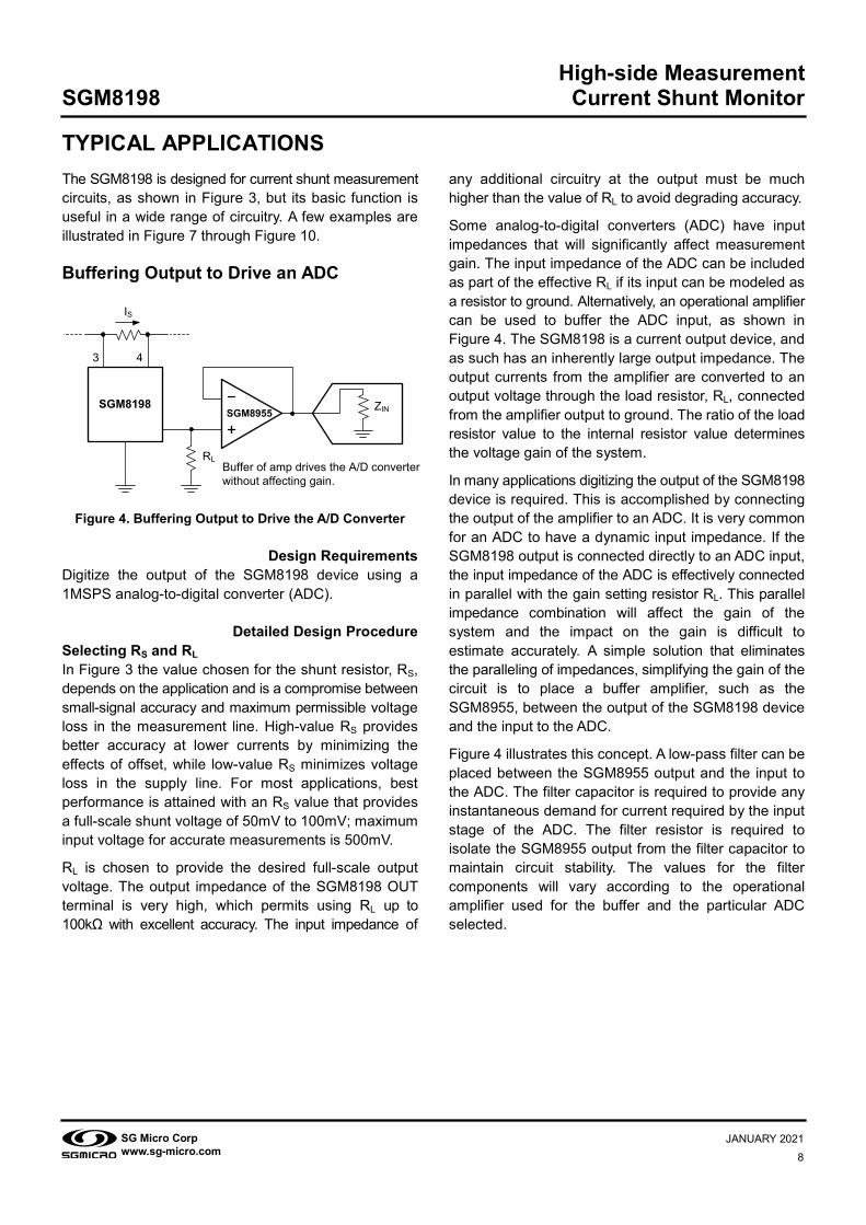
TYPICAL APPLICATIONS The SGM8198 is designed for current shunt measurement circuits, as shown in Figure 3, but its basic function is useful in a wide range of circuitry. A few examples are illustrated in Figure 7 through Figure 10. Buffering Output to Drive an ADC
Figure 4. Buffering Output to Drive the A/D Converter
Design Requirements
Digitize the output of the SGM8198 device using a 1MSPS analog-to-digital converter (ADC).
Detailed Design Procedure Selecting RS and RL In Figure 3 the value chosen for the shunt resistor, RS, depends on the application and is a compromise between small-signal accuracy and maximum permissible voltage loss in the measurement line. High-value RS provides better accuracy at lower currents by minimizing the effects of offset, while low-value RS minimizes voltage loss in the supply line. For most applications, best performance is attained with an RS value that provides a full-scale shunt voltage of 50mV to 100mV; maximum input voltage for accurate measurements is 500mV.
RL is chosen to provide the desired full-scale output voltage. The output impedance of the SGM8198 OUT terminal is very high, which permits using RL up to 100kΩ with excellent accuracy. The input impedance of
any additional circuitry at the output must be much higher than the value of RL to avoid degrading accuracy.
Some analog-to-digital converters (ADC) have input impedances that will significantly affect measurement gain. The input impedance of the ADC can be included as part of the effective RL if its input can be modeled as a resistor to ground. Alternatively, an operational amplifier can be used to buffer the ADC input, as shown in Figure 4. The SGM8198 is a current output device, and as such has an inherently large output impedance. The output currents from the amplifier are converted to an output voltage through the load resistor, RL, connected from the amplifier output to ground. The ratio of the load resistor value to the internal resistor value determines the voltage gain of the system.
In many applications digitizing the output of the SGM8198 device is required. This is accomplished by connecting the output of the amplifier to an ADC. It is very common for an ADC to have a dynamic input impedance. If the SGM8198 output is connected directly to an ADC input, the input impedance of the ADC is effectively connected in parallel with the gain setting resistor RL. This parallel impedance combination will affect the gain of the system and the impact on the gain is difficult to estimate accurately. A simple solution that eliminates the paralleling of impedances, simplifying the gain of the circuit is to place a buffer amplifier, such as the SGM8955, between the output of the SGM8198 device and the input to the ADC.
Figure 4 illustrates this concept. A low-pass filter can be placed between the SGM8955 output and the input to the ADC. The filter capacitor is required to provide any instantaneous demand for current required by the input stage of the ADC. The filter resistor is required to isolate the SGM8955 output from the filter capacitor to maintain circuit stability. The values for the filter components will vary according to the operational amplifier used for the buffer and the particular ADC selected.
RL
IS
3 4
ZINSGM8955
Buffer of amp drives the A/D converter without affecting gain.
SGM8198

High-side Measurement SGM8198 Current Shunt Monitor
9 JANUARY 2021 SG Micro Corp
www.sg-micro.com
TYPICAL APPLICATIONS (Continued) Output Filter
RL
3 4
SGM8198
CL
VOUT
f-3dB
-3dBL L
1f2 R C
=π
Figure 5. Output Filter
Design Requirements Filter the output of the SGM8198 device.
Detailed Design Procedure A low-pass filter can be formed at the output of the SGM8198 device simply by placing a capacitor of the desired value in parallel with the load resistor. First, determine the value of the load resistor needed to achieve the desired gain. See the table in Figure 3. Next, determine the capacitor value that will result in the desired cutoff frequency according to the equation shown in Figure 5. Figure 6 illustrates various combinations of gain settings (determined by RL) and filter capacitors.
Application Curve
Figure 6. Gain vs. Frequency
Offsetting the Output Voltage For many applications using only a single power supply, it may be required to level shift the output voltage away from ground when there is no load current flowing in the shunt resistor. Level shifting the output of the SGM8198 device is easily accomplished by one of the two simple methods shown in Figure 7. The method on the left- hand side of Figure 7 illustrates a simple voltage divider method. This method is useful for applications that require the output of the SGM8198 device to remain centered with respect to the power supply at zero load current through the shunt resistor. Using this method, the gain is determined by the parallel combination of R1 and R2 while the output offset is determined by the voltage divider ratio R1 and R2. For applications that may require a fixed value of output offset, independent of the power supply voltage, the current source method shown on the right-hand side of Figure 7 is recommended. With this method, a constant current source is used to generate a constant output offset. Using this method, the gain is determined by RL and the offset is determined by the product of the value of the current source and RL.
3 4
SGM8198
VOUT1
RL
100μA
VCC
Gain Set by RL
Output Offset = (100μA) (RL)(independent of VCC)b) Using current source.
3 4
SGM8198
VOUT1
R2
R1
VR
Gain Set by R1 || R2
Output Offset = (VR) R2R1 + R2
a) Using resistor divider.
Figure 7. Offsetting the Output Voltage
-40
-20
0
20
40
60
0.1 1 10 100 1000 10000
Gai
n (d
B)
Frequency (kHz)
RL = 1kΩ
RL = 10kΩ
RL = 100kΩ
High-side Measurement SGM8198 Current Shunt Monitor
10 JANUARY 2021 SG Micro Corp
www.sg-micro.com
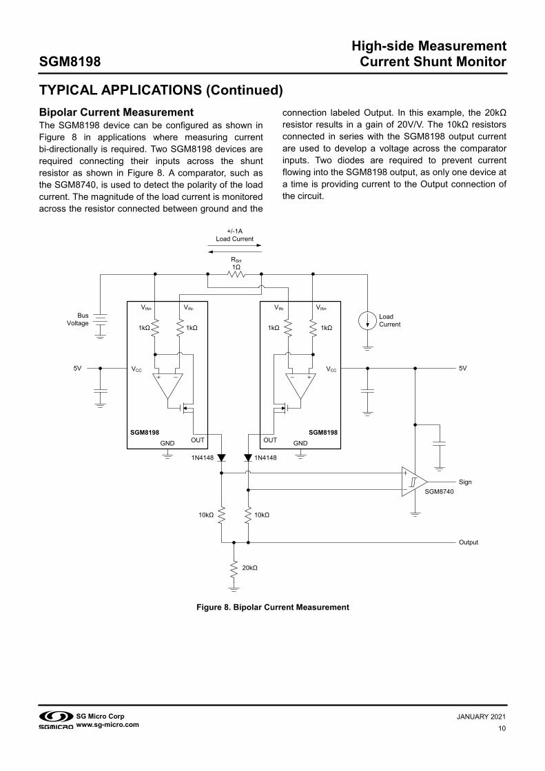
TYPICAL APPLICATIONS (Continued) Bipolar Current Measurement The SGM8198 device can be configured as shown in Figure 8 in applications where measuring current bi-directionally is required. Two SGM8198 devices are required connecting their inputs across the shunt resistor as shown in Figure 8. A comparator, such as the SGM8740, is used to detect the polarity of the load current. The magnitude of the load current is monitored across the resistor connected between ground and the
connection labeled Output. In this example, the 20kΩ resistor results in a gain of 20V/V. The 10kΩ resistors connected in series with the SGM8198 output current are used to develop a voltage across the comparator inputs. Two diodes are required to prevent current flowing into the SGM8198 output, as only one device at a time is providing current to the Output connection of the circuit.
VIN+ VIN-
GND
1kΩ 1kΩ
SGM8198
VCC
OUT
VIN+VIN-
GND
1kΩ 1kΩ
SGM8198
VCC
OUT
10kΩ 10kΩ
Bus Voltage
5V 5V
1N4148 1N4148
20kΩ
Load Current
SGM8740Sign
Output
RSH1Ω
+/-1ALoad Current
Figure 8. Bipolar Current Measurement
High-side Measurement SGM8198 Current Shunt Monitor
11 JANUARY 2021 SG Micro Corp
www.sg-micro.com
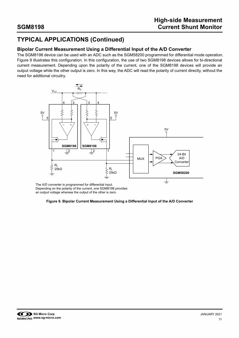
TYPICAL APPLICATIONS (Continued) Bipolar Current Measurement Using a Differential Input of the A/D Converter The SGM8198 device can be used with an ADC such as the SGM58200 programmed for differential mode operation. Figure 9 illustrates this configuration. In this configuration, the use of two SGM8198 devices allows for bi-directional current measurement. Depending upon the polarity of the current, one of the SGM8198 devices will provide an output voltage while the other output is zero. In this way, the ADC will read the polarity of current directly, without the need for additional circuitry.
RS
5V
SGM819812
3 4
55V
SGM81981 2
34
5
RL25kΩ
RL25kΩ
VCC
SGM58200
The A/D converter is programmed for differential input.Depending on the polarity of the current, one SGM8198 provides an output voltage whereas the output of the other is zero.
MUX PGA24-Bit A/D
Converter
5V
Figure 9. Bipolar Current Measurement Using a Differential Input of the A/D Converter
High-side Measurement SGM8198 Current Shunt Monitor
12 JANUARY 2021 SG Micro Corp
www.sg-micro.com
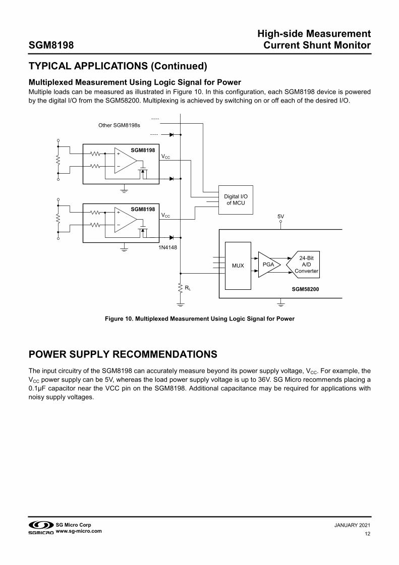
TYPICAL APPLICATIONS (Continued) Multiplexed Measurement Using Logic Signal for Power Multiple loads can be measured as illustrated in Figure 10. In this configuration, each SGM8198 device is powered by the digital I/O from the SGM58200. Multiplexing is achieved by switching on or off each of the desired I/O.
RL
SGM8198
SGM8198VCC
VCC
Other SGM8198s
1N4148
SGM58200
MUX PGA24-Bit A/D
Converter
5V
Digital I/O of MCU
Figure 10. Multiplexed Measurement Using Logic Signal for Power POWER SUPPLY RECOMMENDATIONS The input circuitry of the SGM8198 can accurately measure beyond its power supply voltage, VCC. For example, the VCC power supply can be 5V, whereas the load power supply voltage is up to 36V. SG Micro recommends placing a 0.1µF capacitor near the VCC pin on the SGM8198. Additional capacitance may be required for applications with noisy supply voltages.
High-side Measurement SGM8198 Current Shunt Monitor
13 JANUARY 2021 SG Micro Corp
www.sg-micro.com
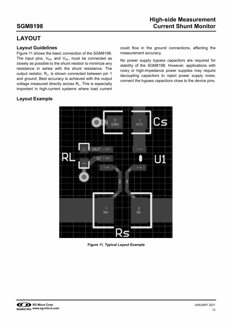
LAYOUT Layout Guidelines Figure 11 shows the basic connection of the SGM8198. The input pins, VIN+ and VIN-, must be connected as closely as possible to the shunt resistor to minimize any resistance in series with the shunt resistance. The output resistor, RL, is shown connected between pin 1 and ground. Best accuracy is achieved with the output voltage measured directly across RL. This is especially important in high-current systems where load current
could flow in the ground connections, affecting the measurement accuracy.
No power supply bypass capacitors are required for stability of the SGM8198. However, applications with noisy or high-impedance power supplies may require decoupling capacitors to reject power supply noise; connect the bypass capacitors close to the device pins.
Layout Example
Figure 11. Typical Layout Example

High-side Measurement SGM8198 Current Shunt Monitor
14 JANUARY 2021 SG Micro Corp
www.sg-micro.com
REVISION HISTORY NOTE: Page numbers for previous revisions may differ from page numbers in the current version. JANUARY 2021 ‒ REV.A.1 to REV.A.2 Page
Updated Absolute Maximum Ratings section ....................................................................................................................................................... 2
AUGUST 2019 ‒ REV.A to REV.A.1 Page
Updated Electrical Characteristics section ........................................................................................................................................................... 3
Changes from Original (DECEMBER 2018) to REV.A Page
Changed from product preview to production data ............................................................................................................................................. All
PACKAGE INFORMATION
TX00033.000 SG Micro Corp www.sg-micro.com
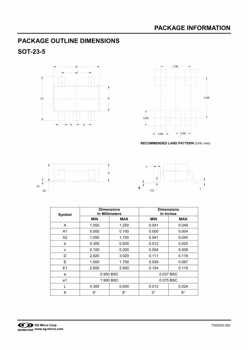
PACKAGE OUTLINE DIMENSIONS SOT-23-5
Symbol Dimensions
In Millimeters Dimensions
In Inches MIN MAX MIN MAX
A 1.050 1.250 0.041 0.049 A1 0.000 0.100 0.000 0.004 A2 1.050 1.150 0.041 0.045 b 0.300 0.500 0.012 0.020 c 0.100 0.200 0.004 0.008 D 2.820 3.020 0.111 0.119 E 1.500 1.700 0.059 0.067
E1 2.650 2.950 0.104 0.116 e 0.950 BSC 0.037 BSC
e1 1.900 BSC 0.075 BSC L 0.300 0.600 0.012 0.024 θ 0° 8° 0° 8°
EE1
e
e1
b
D
A1A2
A
c
L
θ0.2
RECOMMENDED LAND PATTERN (Unit: mm)
1.90
2.59
0.99
0.69 0.95

PACKAGE INFORMATION
TX10000.000 SG Micro Corp www.sg-micro.com
TAPE AND REEL INFORMATION NOTE: The picture is only for reference. Please make the object as the standard.
KEY PARAMETER LIST OF TAPE AND REEL
Package Type Reel Diameter
Reel Width W1
(mm) A0
(mm) B0
(mm) K0
(mm) P0
(mm) P1
(mm) P2
(mm) W
(mm) Pin1
Quadrant
DD
0001 SOT-23-5 7″ 9.5 3.20 3.20 1.40 4.0 4.0 2.0 8.0 Q3
Reel Width (W1)
Reel Diameter
REEL DIMENSIONS
TAPE DIMENSIONS
DIRECTION OF FEED
P2 P0
W
P1 A0 K0
B0Q1 Q2
Q4Q3 Q3 Q4
Q2Q1
Q3 Q4
Q2Q1

PACKAGE INFORMATION
TX20000.000 SG Micro Corp www.sg-micro.com
CARTON BOX DIMENSIONS NOTE: The picture is only for reference. Please make the object as the standard.
KEY PARAMETER LIST OF CARTON BOX
Reel Type Length (mm)
Width (mm)
Height (mm) Pizza/Carton
DD
0002
7″ (Option) 368 227 224 8
7″ 442 410 224 18