shaping and homogenization of led white light using ... · shaping and homogenization of led white...
TRANSCRIPT
Shaping and Homogenization of LED
White Light Using Aperiodic Scattering
Cells Array
Huiying Zhong, Roberto Knoth, Christian Hellmann, Liangxin Yang,
Frank Wyrowski
SPIE 10379-12

Background / Motivation
• Homogenization and shaping of LED white light is
interesting for industrial applications.
2

Background / Motivation
• Homogenization and shaping of LED white light is
interesting for industrial applications.
Task: Homogenization and shaping of LED white
light !
3
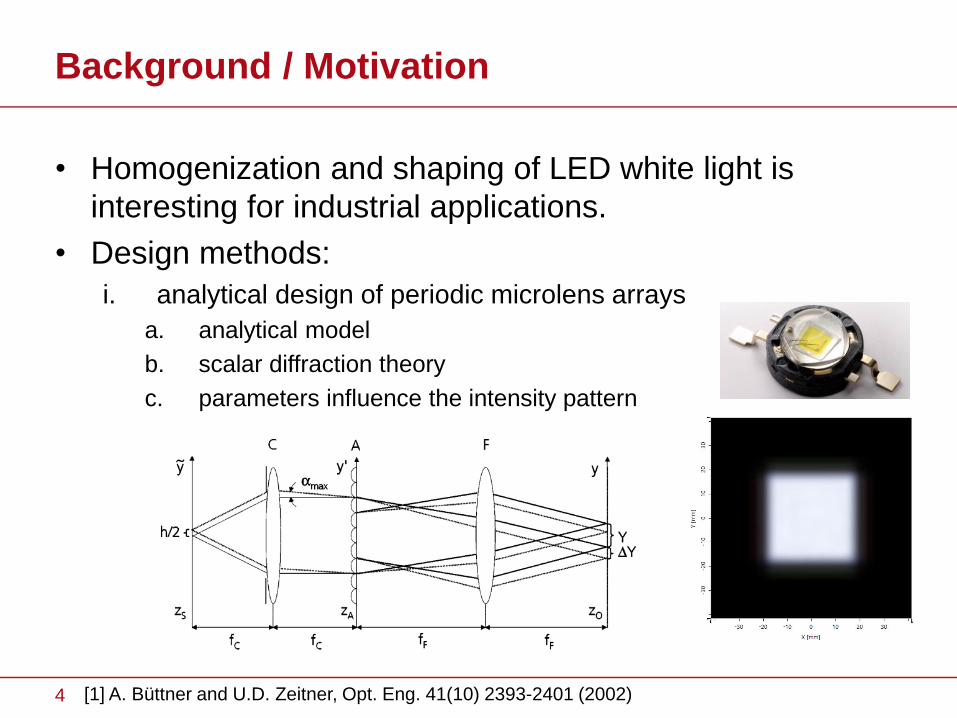
Background / Motivation
• Homogenization and shaping of LED white light is
interesting for industrial applications.
• Design methods:
i. analytical design of periodic microlens arrays
a. analytical model
b. scalar diffraction theory
c. parameters influence the intensity pattern
[1] A. Büttner and U.D. Zeitner, Opt. Eng. 41(10) 2393-2401 (2002)4
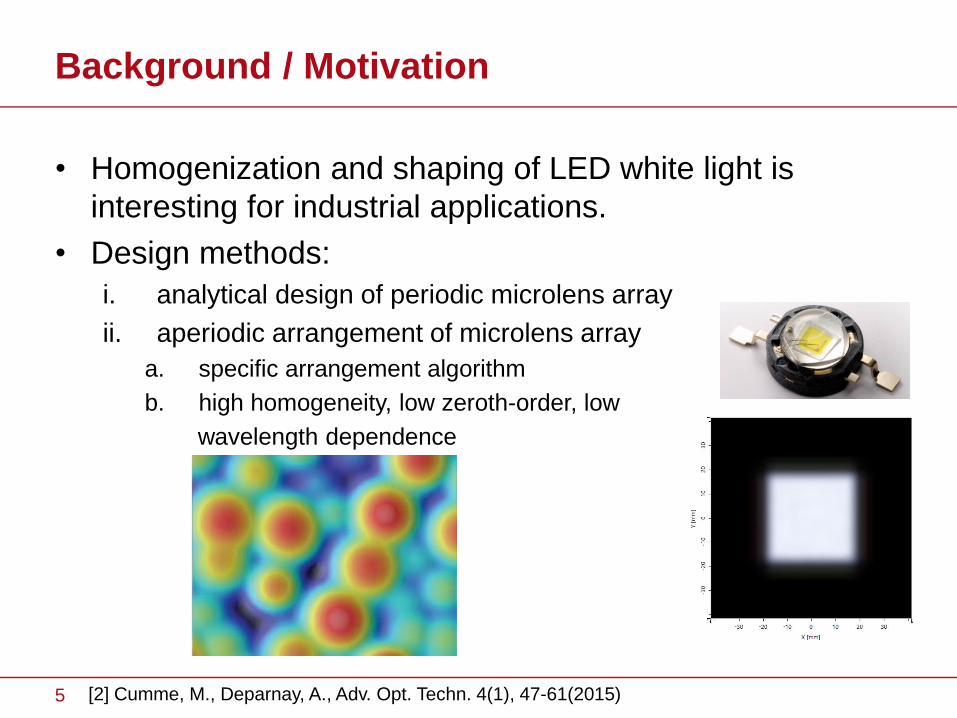
Background / Motivation
• Homogenization and shaping of LED white light is
interesting for industrial applications.
• Design methods:
i. analytical design of periodic microlens array
ii. aperiodic arrangement of microlens array
a. specific arrangement algorithm
b. high homogeneity, low zeroth-order, low
wavelength dependence
[2] Cumme, M., Deparnay, A., Adv. Opt. Techn. 4(1), 47-61(2015)5

Background / Motivation
• Homogenization and shaping of LED white light is
interesting for industrial applications.
• Design methods:
i. analytical design of periodic microlens array
ii. aperiodic arrangement of microlens array
• In this talk,
i. advance modeling of the optical system
ii. the design procedure starts from
analytical design of a periodic microlens
array
iii. apply the probability function to achieve an
aperiodic microlens array to increase the
homogeneity
6
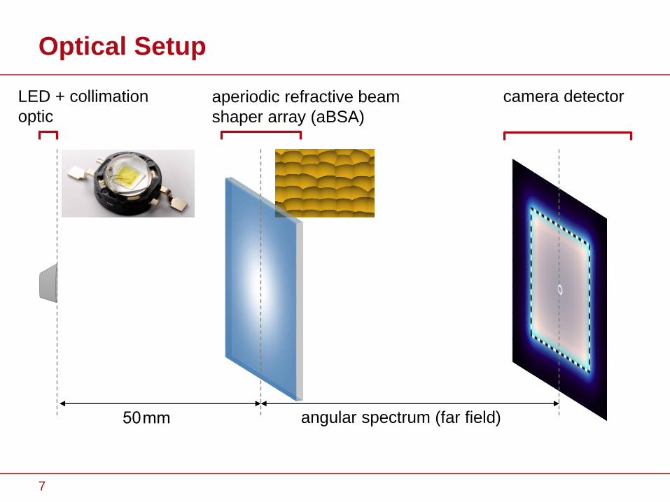
Optical Setup
50 mm angular spectrum (far field)
LED + collimation
optic
aperiodic refractive beam
shaper array (aBSA)
camera detector
7

Optical Setup
50 mm angular spectrum (far field)
LED + collimation
optic
aperiodic refractive beam
shaper array (aBSA)
camera detector
How to model the source, element and detector?
8
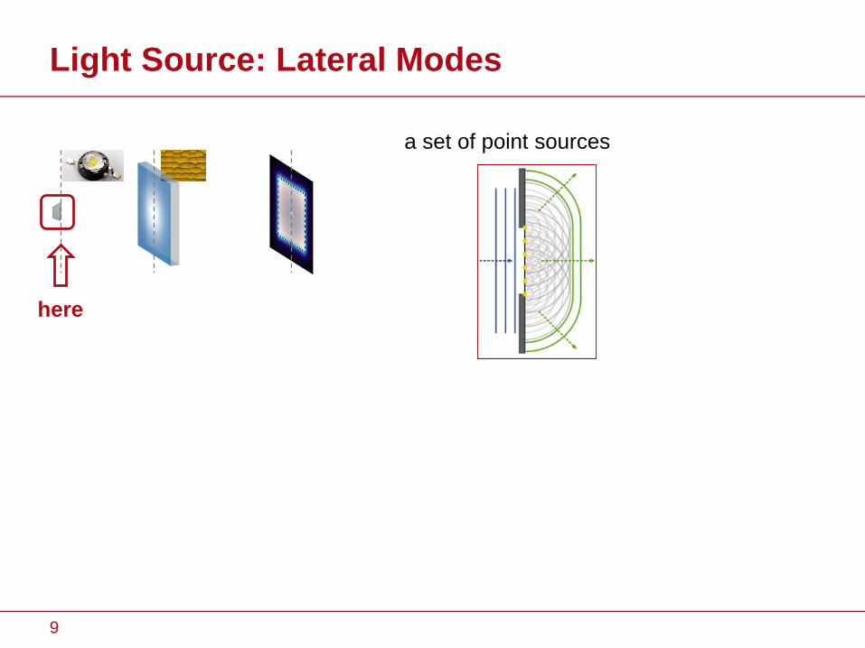
Light Source: Lateral Modes
here
a set of point sources
9

Light Source: Lateral Modes
here
shifted- elementary-mode concept
[3] Tervo, J., Turunen, J., Vahimaa, P. and Wyrowski, F. J. Opt. Soc. Am. A 27(9)(2014)10

Light Source: Lateral Modes
here
intensity distribution after collimation lens
position wavelength 𝐸𝑥 𝐸𝑦
11 [3] Tervo, J., Turunen, J., Vahimaa, P. and Wyrowski, F. J. Opt. Soc. Am. A 27(9)(2014)

Parameter Description / Value & Unit
name/type Seoul Z-LED P4 from Seoul Semiconductors
partially coherent source type Gaussian type planar source
collimation TIR lens from Carclo Optics (part no. 10003)
spectrum pure white light spectrum
FWHM radiant intensity 9°
chip size 200 um x 200 um
Light Source: Lateral Modes
radiant intensity
here
12

Light Source: Spectrum Modes
spectrum model
here
post-processing step to calculate the weight
on each sampled wavelength:
Spectrum′s Integral
≈1
𝑁−0σ𝑖=0𝑁−1 𝑖+1 − 𝑖 (𝐼𝑖+1+ 𝐼𝑖)
= σ𝑖=0𝑁 𝛼𝑖 ∙ 𝐼𝑖
with 𝛼𝑖 =𝜆𝑖−𝜆𝑖−1
𝜆𝑖−𝜆0
13

Components: Lens Array
Parameter Description / Value
cell array aperture 20 x 20 mm
pitch to be designed
substrate thickness 1 mm
substrate material fused silica
here
Thin element (thin lens) approximation:
• paraxial light
• component element is thin enough
14
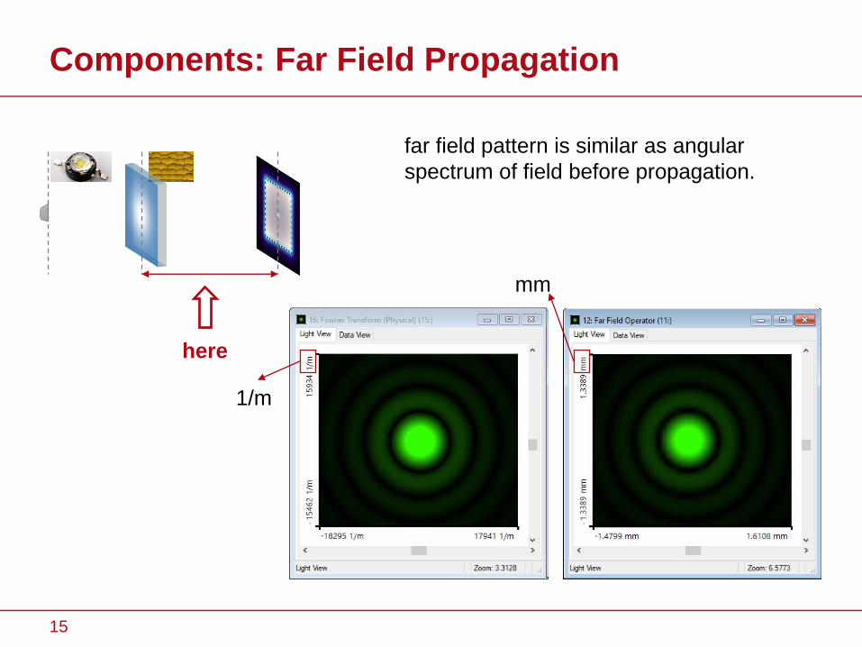
Components: Far Field Propagation
here
far field pattern is similar as angular
spectrum of field before propagation.
1/m
mm
15
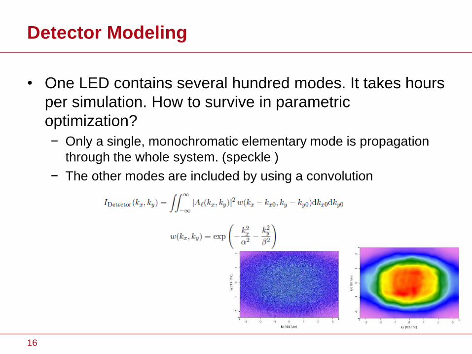
Detector Modeling
• One LED contains several hundred modes. It takes hours
per simulation. How to survive in parametric
optimization?
− Only a single, monochromatic elementary mode is propagation
through the whole system. (speckle )
− The other modes are included by using a convolution
16
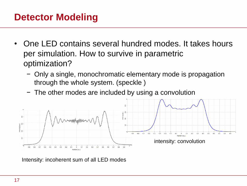
Detector Modeling
• One LED contains several hundred modes. It takes hours
per simulation. How to survive in parametric
optimization?
− Only a single, monochromatic elementary mode is propagation
through the whole system. (speckle )
− The other modes are included by using a convolution
Intensity: incoherent sum of all LED modes
intensity: convolution
17
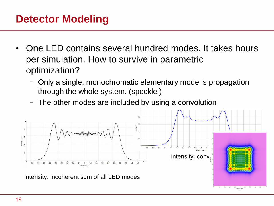
Detector Modeling
• One LED contains several hundred modes. It takes hours
per simulation. How to survive in parametric
optimization?
− Only a single, monochromatic elementary mode is propagation
through the whole system. (speckle )
− The other modes are included by using a convolution
Intensity: incoherent sum of all LED modes
intensity: convolution
18
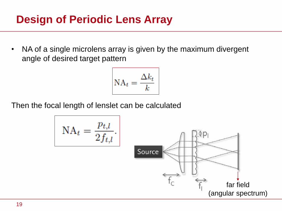
Design of Periodic Lens Array
• NA of a single microlens array is given by the maximum divergent
angle of desired target pattern
Then the focal length of lenslet can be calculated
19
far field
(angular spectrum)

• Lens array is periodic, so in far field, several diffraction orders of one
single incident mode. Order separation is related to pitch size of lens
array:
• Modes with different positions generate a shift
in the angular spectrum. The maximum shift is
given by LED chip size:
• Criterial: 𝛿𝑘𝑡 ≪ 𝛿𝑘𝑡,shift
Design of Periodic Lens Array
far field
(angular spectrum)
20

Result page of periodic lens array
21
Parameter Description / Value &
Unit
cell array aperture 20 x 20 mm
pitch 161.5 µm
FWHM window
function 𝛿𝑘𝑡,shift
1.56E6 1/m
Parameter Initial Optimized
NA 0.1736 0.1785
focal length 465.02 µm 452.36 µm
profile height 15.62 µm 16.10 µm
simulated FWHM 4.60E6 1/m 4.84E6 1/m
conversion effc. 80.18 84.22
uniformity error 49.63 43.08

Design of Aperiodic Lens arrays
• Center of each lenslet:
• The height of microlens array is determined by selecting the highest
height value of current cell and the corresponding 8 adjacent cells:
22

Design of Aperiodic Lens arrays
• During the optimization, we keep the parameters of each lenslet
identical. The variables are:
Probability function
23
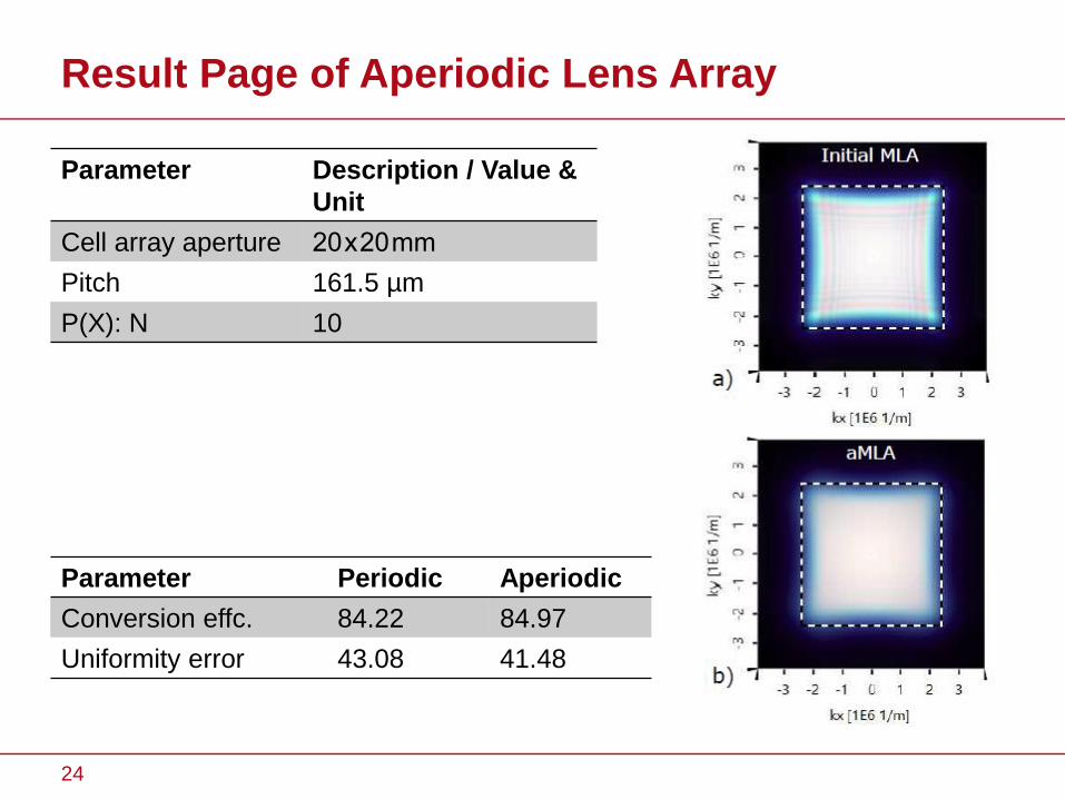
Result Page of Aperiodic Lens Array
24
Parameter Description / Value &
Unit
Cell array aperture 20 x 20 mm
Pitch 161.5 µm
P(X): N 10
Parameter Periodic Aperiodic
Conversion effc. 84.22 84.97
Uniformity error 43.08 41.48
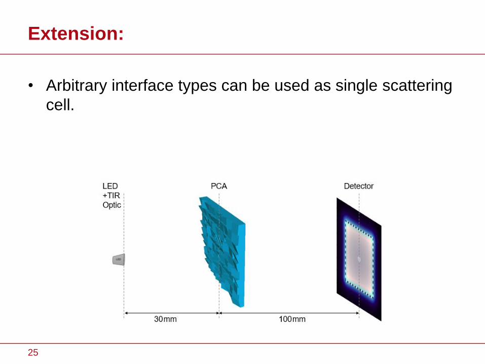
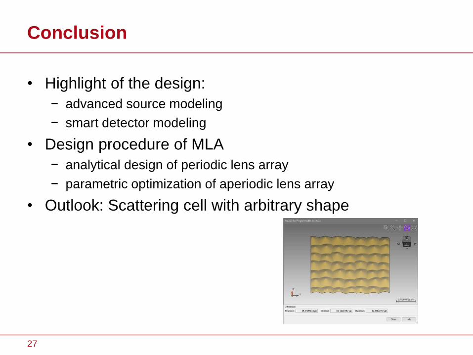
Extension:
• Arbitrary interface types can be used as single scattering
cell.
25
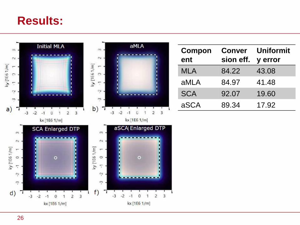
Results:
26
Compon
ent
Conver
sion eff.
Uniformit
y error
MLA 84.22 43.08
aMLA 84.97 41.48
SCA 92.07 19.60
aSCA 89.34 17.92
Conclusion
• Highlight of the design:
− advanced source modeling
− smart detector modeling
• Design procedure of MLA
− analytical design of periodic lens array
− parametric optimization of aperiodic lens array
• Outlook: Scattering cell with arbitrary shape
27

Acknowledgement
• Zentrales Innovationsprogramm Mittelstand(ZIM)-
Kooperationsprojecte
28

Thanks for your attention!
29