shaping plasmon beams via the controlled illumination of ... · shaping plasmon beams via the...
TRANSCRIPT
Shaping plasmon beams via thecontrolled illumination of finite-sizeplasmonic crystalsJ.-S. Bouillard*, P. Segovia, W. Dickson, G. A. Wurtz & A. V. Zayats
Department of Physics, King’s College London, Strand, London WC2R 2LS, United Kingdom.
Plasmonic crystals provide many passive and active optical functionalities, including enhanced sensing,optical nonlinearities, light extraction from LEDs and coupling to and from subwavelength waveguides.Here we study, both experimentally and numerically, the coherent control of SPP beam excitation in finitesize plasmonic crystals under focussed illumination. The correct combination of the illuminating spot size,its position relative to the plasmonic crystal, wavelength and polarisation enables the efficient shaping anddirectionality of SPP beam launching. We show that under strongly focussed illumination, the illuminatedpart of the crystal acts as an antenna, launching surface plasmon waves which are subsequently filtered bythe surrounding periodic lattice. Changing the illumination conditions provides rich opportunities toengineer the SPP emission pattern. This offers an alternative technique to actively modulate and controlplasmonic signals, either via micro- and nano-electromechanical switches or with electro- and all-opticalbeam steering which have direct implications for the development of new integrated nanophotonic devices,such as plasmonic couplers and switches and on-chip signal demultiplexing. This approach can begeneralised to all kinds of surface waves, either for the coupling and discrimination of light in planardielectric waveguides or the generation and control of non-diffractive SPP beams.
The coherent control of optical waves by shaping the phase and amplitude of interfering wavefronts hasrecently resulted in significant progress in non-diffracting optical and surface plasmon polariton (SPP)beam1–3 routing, directional coupling, optical signal switching4–6 and flat lenses7,8 as well as new types of
holograms9,10. SPP waves, important for applications in sensing, nonlinear optics and optical interconnectapplications, are uniquely positioned to take advantage of a coherent control approach as in many cases, onetype of nanostructures or another, e.g., particles, grooves, plasmonic crystals, are used to couple optical signals toSPP waves and control the SPP propagation direction11–14. Thus, the phase of the SPP beams can be designed at thepoint where controlled coupling of optical beams to SPPs takes place. Further adjusting the position of additionalscatterers to modify both the direction and phase during SPP-in-SPP scattering, provides the freedom of designrequired to achieve phase and amplitude control. This has been used to achieve efficient launchers for SPPs and, inparticular, finite-size SPP beams (including non-diffracting SPPs) by controlling the separation between andwidth of the grooves as well as building more complex optical antennas2,3,15–17. Unidirectional, wavelength-selective and broadband photon-to-SPP and SPP-to-photon scattering have been demonstrated using thisapproach16,18–20.
SPP crystals (SPPCs) — metal surfaces periodically structured on the SPP wavelength scale — have gainedincreasing attention due to their ability to control SPP generation and propagation through easily geometricallyadjustable parameters such as the period or primitive cell geometry of the crystal. In analogy with photoniccrystals, the interaction of SPPs with the plasmonic crystal lattice leads to the creation of SPP Bloch modes as theeigenmodes of the crystal. The geometry of the crystal determines the dispersion of these modes, which ultimatelygoverns the propagation of plasmon waves on the nanostructured area as well as their interaction with illumin-ating light11,21–30. SPPCs have been widely studied, both in the far-field and near-field, however, the vast majorityof studies consider either plane wave illumination of the entire crystal, when the whole structure responds in acollective fashion, or their interaction with SPP illumination coming from the unstructured area.
Under collimated illumination, light interaction with plasmonic crystals involves the resonant excitation of thecrystal’s SPP Bloch modes at frequencies and in directions determined by the overlap with the spectrum ofallowed SPP states and the polarisation of the excitation light11,21,23. While such considerations are generally validonly for infinite crystals, the effects of finite size plasmonic crystals is accounted for by considering the effects of
OPEN
SUBJECT AREAS:NANOPHOTONICS AND
PLASMONICS
METAMATERIALS
OPTOELECTRONIC DEVICES ANDCOMPONENTS
OPTICAL SPECTROSCOPY
Received28 July 2014
Accepted31 October 2014
Published28 November 2014
Correspondence andrequests for materials
should be addressed toP.S.O. (paulina.
*Current address:Department of Physics
and Mathematics,University of Hull,Cottingham Road,
Hull, HU6 7RX, UnitedKingdom.
SCIENTIFIC REPORTS | 4 : 7234 | DOI: 10.1038/srep07234 1

the boundary on Bloch mode propagation: at the interface betweenthe nanostructured and unstructured areas, the Bloch modes arerefracted, thus allowing for efficient excitation of SPPs onto thesmooth metal film surrounding the plasmonic crystal via transmis-sion through the interface22,23,29,31.
However, the focussed illumination of plasmonic crystals differsfrom the collimated one in three important ways. Firstly, focusinggenerates a distribution of wavevectors in the incident light beaminteracting with the nanostructured area and hence introduces thepossibility of simultaneously exciting multiple Bloch modes withdifferent momenta. Secondly, for strongly focussed beams the polar-isation in the focal plane has various components not present in thecollimated beam. Finally, the number of unit cells illuminated isgreatly reduced due to the reduction in the illumination spot size,so that SPPs generated in one part of the crystal are free to propagatethrough the crystal without interfering with SPPs generated else-where, as would be the case were the crystal under plane waveillumination.
In this work, SPP beam excitation inside and outside plasmoniccrystals under focussed illumination is investigated experimentallyusing hyperspectral near-field imaging. The experimental results arerationalised theoretically using a vectorial dipolar model accountingfor multiple SPP scattering. The simultaneous excitation and pro-pagation of different order Bloch modes on the nanostructured areaand their transmission through the crystal’s interface onto thesmooth metal film have been studied. The sensitivity of the propaga-tion direction and shape of the plasmonic beams to the illuminationconditions were investigated. The results presented in this work openup new opportunities for designing novel SPP launchers providingboth beam shape and direction control. Furthermore, this work hasstrong implications for the design of ultra-fast active plasmonicdevices using SPPCs, where the switching and directing of signalSPP beams can be achieved by, e.g., electo-optical, all-optical orelectro-mechanical control of the size, position and/or polarisationof the excitation beam.
ResultsThe effects of focussed illumination on the plasmonic behaviour ofSPPCs were investigated on a 2D crystal comprised of circular holesof 200 nm diameter arranged in a square lattice with a periodicity of600 nm. The overall size of the crystal is approximately 20 3 20 mm2,corresponding to 33 lattice periods (Fig. 1a). The dispersion of theSPP Bloch modes supported by the crystal, as characterized by plane-
wave illumination, exhibits the usual system of allowed and forbid-den bands (Fig. 1b, c). The near-field behaviour of the plasmoniccrystal under focussed illumination was experimentally probed fortwo different numerical apertures (NA): 0.45 and 0.9. For both NAsconsidered in this work, the size of the Gaussian-shaped illuminationspot on the plasmonic crystal is about 1 mm in diameter (FWHM),therefore only a 2 3 2 array of holes is illuminated (see Methods).
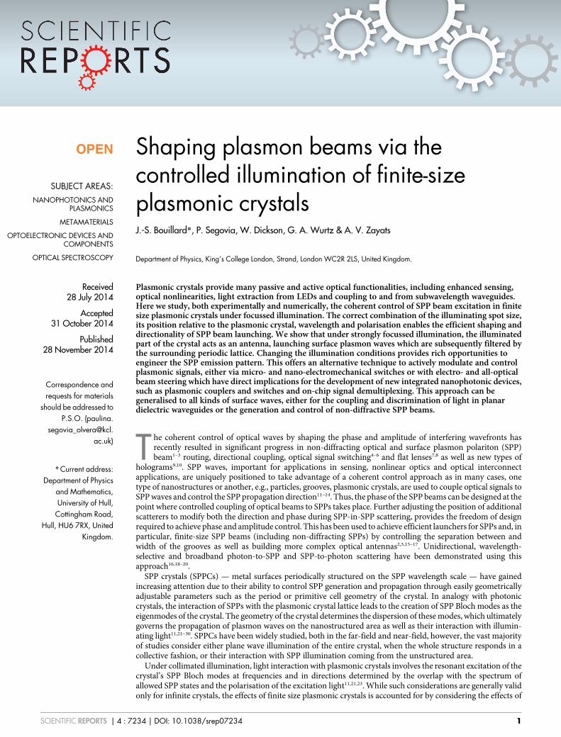
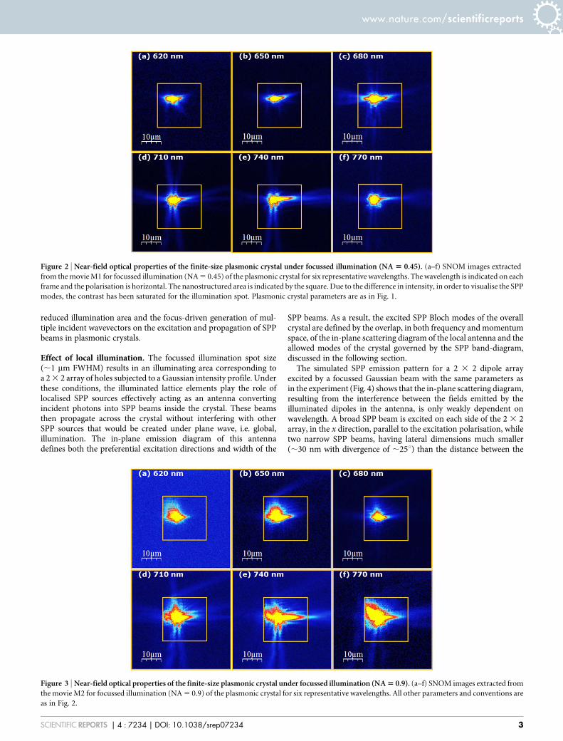
In contrast to the behaviour of the crystal under collimated (planewave) illumination, where SPP waves with a width determined by thecrystal size are excited (see, e.g., Refs. 15,22,23,29), focussed illumina-tion generates SPP beams of widths much smaller than the size of thecrystal and with different propagation directions both inside andoutside the crystal (Fig. 2(a–f) and movie M1 for NA 5 0.45 andFig. 3(a–f) and movie M2 for NA 5 0.9). For both focusing condi-tions considered here, SPP beams of reduced spatial widths propagateon the crystal preferentially in both the (1,0) and (0,1) directions forwavelengths exceeding 650 nm. For shorter wavelengths SPP beamspropagating in the (1,1) directions are also observed. Increasing therange of wavevectors present in the illumination even further bytighter focusing (Fig. 3) leads to a more complex near-field distri-bution as the (1,1) Bloch modes are then observed across the entirewavelength range considered. This behaviour is consistent with thecalculated dispersion of the crystal (Fig. 1(c)) which indicates that forthe range of incident wavevectors corresponding to both illuminationconditions, the lattice supports (1/21,0) modes, propagating ineither the x or y direction throughout the wavelength range understudy. However, the wavevector spectrum provided by an NA of 0.45can only populate the (1,1) modes, propagating at 45u to the latticeprincipal axes, for wavelengths shorter than 655 nm, whereas thelarger range of wavevectors provided by an NA of 0.9, allows forthe excitation of the these modes across the entire spectral range.
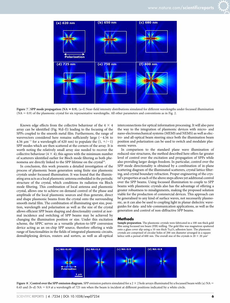
At the crystal boundaries, both the reflection back into the crystaland transmission onto the smooth film of SPP beams can beobserved. Using the larger NA of 0.9 enables observation of thestrong refraction of the (1,1) modes as they are now populated atfrequencies having propagation lengths which are sufficiently long toreach and interact with the crystal boundary. In this case, the (1/21,0) modes refract at normal incidence since the crystal boundaryis perpendicular to the (1/21,0) directions.
DiscussionIn order to understand the complex near-field distributions observedexperimentally, it is necessary to consider the effects of both the
Figure 1 | The plasmonic crystal and its SPP mode structure. (a) Scanning electron microscope (SEM) image of the plasmonic crystal with period
600 nm and hole diameter 200 nm. Inset shows the schematics of the sample geometry. (b) Far-field transmission dispersion of the crystal in (a)
measured with p-polarised incident light. The calculated spectrum of Bragg-scattered SPPs, representing the Bloch modes of the crystal, is super-imposed
onto the experimental data along with the SPP modes at the Au-air interface (blue) and the Au-glass interface (red). (c) Empty lattice model calculations
of the SPP Bloch modes dispersion showing boundaries of the first Brillouin zone of the crystal for the Au-air interface in theC-X and theC-M directions.
The parts of the dispersion corresponding to the range of incident angles accessible with the illumination through the objectives with the NA of 0.45 and
0.9 are shown in dark and light grey, respectively.
www.nature.com/scientificreports
SCIENTIFIC REPORTS | 4 : 7234 | DOI: 10.1038/srep07234 2
reduced illumination area and the focus-driven generation of mul-tiple incident wavevectors on the excitation and propagation of SPPbeams in plasmonic crystals.
Effect of local illumination. The focussed illumination spot size(,1 mm FWHM) results in an illuminating area corresponding toa 2 3 2 array of holes subjected to a Gaussian intensity profile. Underthese conditions, the illuminated lattice elements play the role oflocalised SPP sources effectively acting as an antenna convertingincident photons into SPP beams inside the crystal. These beamsthen propagate across the crystal without interfering with otherSPP sources that would be created under plane wave, i.e. global,illumination. The in-plane emission diagram of this antennadefines both the preferential excitation directions and width of the
SPP beams. As a result, the excited SPP Bloch modes of the overallcrystal are defined by the overlap, in both frequency and momentumspace, of the in-plane scattering diagram of the local antenna and theallowed modes of the crystal governed by the SPP band-diagram,discussed in the following section.
The simulated SPP emission pattern for a 2 3 2 dipole arrayexcited by a focussed Gaussian beam with the same parameters asin the experiment (Fig. 4) shows that the in-plane scattering diagram,resulting from the interference between the fields emitted by theilluminated dipoles in the antenna, is only weakly dependent onwavelength. A broad SPP beam is excited on each side of the 2 3 2array, in the x direction, parallel to the excitation polarisation, whiletwo narrow SPP beams, having lateral dimensions much smaller(,30 nm with divergence of ,25u) than the distance between the
Figure 2 | Near-field optical properties of the finite-size plasmonic crystal under focussed illumination (NA 5 0.45). (a–f) SNOM images extracted
from the movie M1 for focussed illumination (NA 5 0.45) of the plasmonic crystal for six representative wavelengths. The wavelength is indicated on each
frame and the polarisation is horizontal. The nanostructured area is indicated by the square. Due to the difference in intensity, in order to visualise the SPP
modes, the contrast has been saturated for the illumination spot. Plasmonic crystal parameters are as in Fig. 1.
Figure 3 | Near-field optical properties of the finite-size plasmonic crystal under focussed illumination (NA 5 0.9). (a–f) SNOM images extracted from
the movie M2 for focussed illumination (NA 5 0.9) of the plasmonic crystal for six representative wavelengths. All other parameters and conventions are
as in Fig. 2.
www.nature.com/scientificreports
SCIENTIFIC REPORTS | 4 : 7234 | DOI: 10.1038/srep07234 3
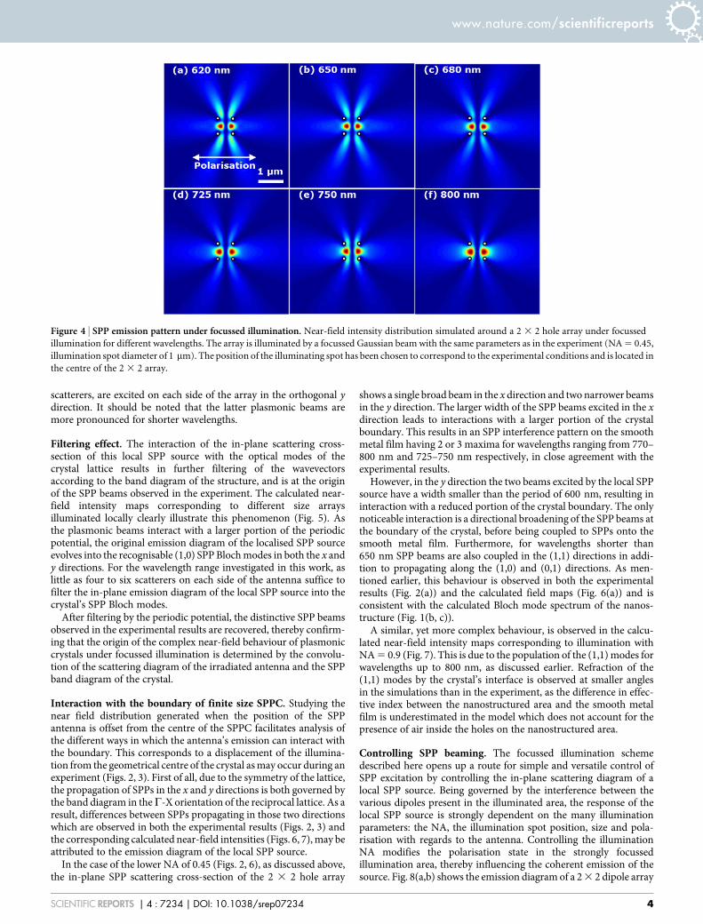
scatterers, are excited on each side of the array in the orthogonal ydirection. It should be noted that the latter plasmonic beams aremore pronounced for shorter wavelengths.
Filtering effect. The interaction of the in-plane scattering cross-section of this local SPP source with the optical modes of thecrystal lattice results in further filtering of the wavevectorsaccording to the band diagram of the structure, and is at the originof the SPP beams observed in the experiment. The calculated near-field intensity maps corresponding to different size arraysilluminated locally clearly illustrate this phenomenon (Fig. 5). Asthe plasmonic beams interact with a larger portion of the periodicpotential, the original emission diagram of the localised SPP sourceevolves into the recognisable (1,0) SPP Bloch modes in both the x andy directions. For the wavelength range investigated in this work, aslittle as four to six scatterers on each side of the antenna suffice tofilter the in-plane emission diagram of the local SPP source into thecrystal’s SPP Bloch modes.
After filtering by the periodic potential, the distinctive SPP beamsobserved in the experimental results are recovered, thereby confirm-ing that the origin of the complex near-field behaviour of plasmoniccrystals under focussed illumination is determined by the convolu-tion of the scattering diagram of the irradiated antenna and the SPPband diagram of the crystal.
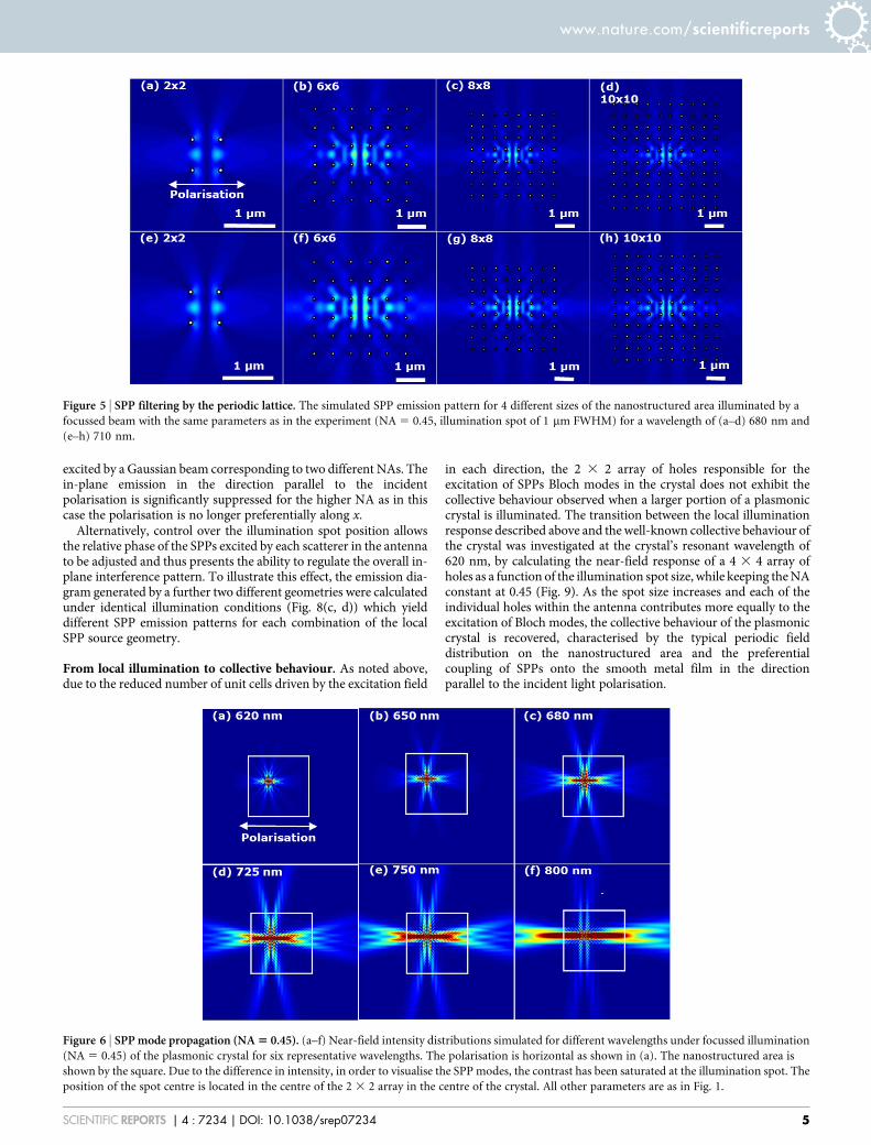
Interaction with the boundary of finite size SPPC. Studying thenear field distribution generated when the position of the SPPantenna is offset from the centre of the SPPC facilitates analysis ofthe different ways in which the antenna’s emission can interact withthe boundary. This corresponds to a displacement of the illumina-tion from the geometrical centre of the crystal as may occur during anexperiment (Figs. 2, 3). First of all, due to the symmetry of the lattice,the propagation of SPPs in the x and y directions is both governed bythe band diagram in theC-X orientation of the reciprocal lattice. As aresult, differences between SPPs propagating in those two directionswhich are observed in both the experimental results (Figs. 2, 3) andthe corresponding calculated near-field intensities (Figs. 6, 7), may beattributed to the emission diagram of the local SPP source.
In the case of the lower NA of 0.45 (Figs. 2, 6), as discussed above,the in-plane SPP scattering cross-section of the 2 3 2 hole array
shows a single broad beam in the x direction and two narrower beamsin the y direction. The larger width of the SPP beams excited in the xdirection leads to interactions with a larger portion of the crystalboundary. This results in an SPP interference pattern on the smoothmetal film having 2 or 3 maxima for wavelengths ranging from 770–800 nm and 725–750 nm respectively, in close agreement with theexperimental results.
However, in the y direction the two beams excited by the local SPPsource have a width smaller than the period of 600 nm, resulting ininteraction with a reduced portion of the crystal boundary. The onlynoticeable interaction is a directional broadening of the SPP beams atthe boundary of the crystal, before being coupled to SPPs onto thesmooth metal film. Furthermore, for wavelengths shorter than650 nm SPP beams are also coupled in the (1,1) directions in addi-tion to propagating along the (1,0) and (0,1) directions. As men-tioned earlier, this behaviour is observed in both the experimentalresults (Fig. 2(a)) and the calculated field maps (Fig. 6(a)) and isconsistent with the calculated Bloch mode spectrum of the nanos-tructure (Fig. 1(b, c)).
A similar, yet more complex behaviour, is observed in the calcu-lated near-field intensity maps corresponding to illumination withNA 5 0.9 (Fig. 7). This is due to the population of the (1,1) modes forwavelengths up to 800 nm, as discussed earlier. Refraction of the(1,1) modes by the crystal’s interface is observed at smaller anglesin the simulations than in the experiment, as the difference in effec-tive index between the nanostructured area and the smooth metalfilm is underestimated in the model which does not account for thepresence of air inside the holes on the nanostructured area.
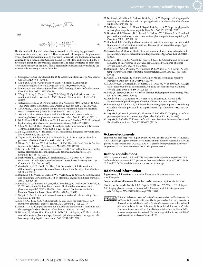
Controlling SPP beaming. The focussed illumination schemedescribed here opens up a route for simple and versatile control ofSPP excitation by controlling the in-plane scattering diagram of alocal SPP source. Being governed by the interference between thevarious dipoles present in the illuminated area, the response of thelocal SPP source is strongly dependent on the many illuminationparameters: the NA, the illumination spot position, size and pola-risation with regards to the antenna. Controlling the illuminationNA modifies the polarisation state in the strongly focussedillumination area, thereby influencing the coherent emission of thesource. Fig. 8(a,b) shows the emission diagram of a 2 3 2 dipole array
Figure 4 | SPP emission pattern under focussed illumination. Near-field intensity distribution simulated around a 2 3 2 hole array under focussed
illumination for different wavelengths. The array is illuminated by a focussed Gaussian beam with the same parameters as in the experiment (NA 5 0.45,
illumination spot diameter of 1 mm). The position of the illuminating spot has been chosen to correspond to the experimental conditions and is located in
the centre of the 2 3 2 array.
www.nature.com/scientificreports
SCIENTIFIC REPORTS | 4 : 7234 | DOI: 10.1038/srep07234 4
excited by a Gaussian beam corresponding to two different NAs. Thein-plane emission in the direction parallel to the incidentpolarisation is significantly suppressed for the higher NA as in thiscase the polarisation is no longer preferentially along x.
Alternatively, control over the illumination spot position allowsthe relative phase of the SPPs excited by each scatterer in the antennato be adjusted and thus presents the ability to regulate the overall in-plane interference pattern. To illustrate this effect, the emission dia-gram generated by a further two different geometries were calculatedunder identical illumination conditions (Fig. 8(c, d)) which yielddifferent SPP emission patterns for each combination of the localSPP source geometry.
From local illumination to collective behaviour. As noted above,due to the reduced number of unit cells driven by the excitation field
in each direction, the 2 3 2 array of holes responsible for theexcitation of SPPs Bloch modes in the crystal does not exhibit thecollective behaviour observed when a larger portion of a plasmoniccrystal is illuminated. The transition between the local illuminationresponse described above and the well-known collective behaviour ofthe crystal was investigated at the crystal’s resonant wavelength of620 nm, by calculating the near-field response of a 4 3 4 array ofholes as a function of the illumination spot size, while keeping the NAconstant at 0.45 (Fig. 9). As the spot size increases and each of theindividual holes within the antenna contributes more equally to theexcitation of Bloch modes, the collective behaviour of the plasmoniccrystal is recovered, characterised by the typical periodic fielddistribution on the nanostructured area and the preferentialcoupling of SPPs onto the smooth metal film in the directionparallel to the incident light polarisation.
Figure 5 | SPP filtering by the periodic lattice. The simulated SPP emission pattern for 4 different sizes of the nanostructured area illuminated by a
focussed beam with the same parameters as in the experiment (NA 5 0.45, illumination spot of 1 mm FWHM) for a wavelength of (a–d) 680 nm and
(e–h) 710 nm.
Figure 6 | SPP mode propagation (NA 5 0.45). (a–f) Near-field intensity distributions simulated for different wavelengths under focussed illumination
(NA 5 0.45) of the plasmonic crystal for six representative wavelengths. The polarisation is horizontal as shown in (a). The nanostructured area is
shown by the square. Due to the difference in intensity, in order to visualise the SPP modes, the contrast has been saturated at the illumination spot. The
position of the spot centre is located in the centre of the 2 3 2 array in the centre of the crystal. All other parameters are as in Fig. 1.
www.nature.com/scientificreports
SCIENTIFIC REPORTS | 4 : 7234 | DOI: 10.1038/srep07234 5
Known edge effects from the collective behaviour of the 4 3 4array can be identified (Fig. 9(d–f)) leading to the focusing of theSPPs coupled to the smooth metal film. Furthermore, the range ofwavevectors considered here remains sufficiently large (24.56 to4.56 mm21 for a wavelength of 620 nm) to populate the (1, 1/21)SPP modes which are then scattered at the corners of the array. It isworth noting the relatively small array size needed to recover thecollective behaviour (4 3 4); this agrees with the minimum numberof scatterers identified earlier for Bloch mode filtering as both phe-nomena are directly linked to the SPP lifetime on the crystal16.
In conclusion, this work presents a detailed investigation of theprocess of plasmonic beam generation using finite size plasmoniccrystals under focussed illumination. It was found that the illumin-ating area acts as a local plasmonic antenna embedded in the periodicstructure of the crystal, which conditions its radiation via Blochmode filtering. This combination of local antenna and plasmoniccrystal, allows one to achieve on-demand control of the phase andamplitude of the local plasmonic sources and thus generate, directand shape plasmonic beams from the crystal onto the surroundingsmooth metal film. The combination of illuminating spot size, posi-tion, wavelength and polarisation as well as the size of the crystalallows efficient SPP beam shaping and directionality control at nor-mal incidence and switching of SPP beams may be achieved bychanging the illumination position or size. Under this excitationscheme, the SPPC serves as a versatile photon-to-SPP conversiondevice acting as an on-chip SPP source, therefore offering a widerange of functionalities in the fields of integrated plasmonic circuits,demultiplexing devices, routers and sorters, as well as all-optical
interconnections for optical information processing. It will also pavethe way to the integration of plasmonic devices with micro- andnano-electromechanical systems (MEMS and NEMS) as well as elec-tro- and all-optical beam steering since both the illumination beamposition and polarization can be used to switch and modulate plas-monic waves.
In comparison to the standard plane wave illumination ofreduced-size structures, the method described here offers far greaterlevel of control over the excitation and propagation of SPPs whilealso providing larger design freedom. In particular, control over theSPP mode directionality is obtained by a combination of in-planescattering diagram of the illuminated scatterers, crystal lattice filter-ing, and crystal boundary refraction. Proper engineering of the crys-tal’s properties at each of the above steps allows yet additional controlover the SPP beams. Using focussed illumination to couple to SPPbeams with plasmonic crystals also has the advantage of offering agreater robustness to misalignments, making the proposed solutionviable for the production of commercial devices. This approach canbe generalised to any kind of surface waves, not necessarily plasmo-nic, as it can also be used to coupling light in planar dielectric wave-guides for data- and tele-communication applications, as well as thegeneration and control of non-diffractive SPP beams.
MethodsSample preparation. The plasmonic crystals were fabricated in a 100 nm thick goldfilm using focussed ion beam (FIB) milling. The gold film was magnetron sputteredonto a glass cover slip using a 10 nm thick Ta2O5 adhesion layer. The plasmoniccrystals are comprised of circular holes of 200 nm diameter arranged in a squarelattice with a period of 600 nm. The overall size of the crystals is 20 3 20 mm2
Figure 7 | SPP mode propagation (NA 5 0.9). (a–f) Near-field intensity distributions simulated for different wavelengths under focussed illumination
(NA 5 0.9) of the plasmonic crystal for six representative wavelengths. All other parameters and conventions as in Fig. 2.
Figure 8 | Control over the SPP emission diagram. SPP emission pattern simulated for a 2 3 2 hole arrays illuminated by a focussed beam with (a) NA 5
0.45 and (b–d) NA 5 0.9 at a wavelength of 725 nm when the beam is incident at different positions indicated by a white circle.
www.nature.com/scientificreports
SCIENTIFIC REPORTS | 4 : 7234 | DOI: 10.1038/srep07234 6

corresponding to 33 lattice periods (Fig. 1a). The dispersion of SPP Bloch modessupported by the crystal represents usual system of allowed and forbidden bands(Fig. 1b, c).
Near-field spectroscopy. In order to directly visualise the SPP interactions withthe plasmonic crystals, a spectroscopic SNOM16,22,32 was used, which allowssimultaneous imaging of the near-field distribution at all wavelengths between400 nm and 1000 nm. Coherent broadband light from a supercontinuum lasersource was used to illuminate the sample from the substrate side. The light is firstinjected into a photonic crystal fibre in order to spatially localise all wavelengthsin the same Gaussian spot which was then collimated using a microscope objective(NA 5 0.2, f 5 22.5 mm) before being polarised and finally focussed onto thesample through a high NA microscope objective (NA 5 0.45, f 5 3.6 mm, or NA5 0.9, f 5 3.0 mm). The size of the illuminated area on the sample, defined by theratio of the focal lengths of the objectives used and the mode extension size in thephotonic crystal fibre, is of the order of 1 mm (FWHM) in both cases. Thestructure was successively illuminated with 2 different microscope objectives andfor each illumination scheme, the near-field images were recorded to allow forcomparison.
The signal collected by the SNOM probe is spectrally separated by a spectrometercoupled to a CCD camera, allowing acquisition of the full near-field spectrum at eachpixel of the SNOM image. The probes used are pulled optical fibres coated with a250 nm gold layer. A nano-aperture with a typical size of the order of 50 nm is createdusing focussed ion beam milling at the tip of the fibre. It should be noted that, basedon a comparison with the numerical simulations, the SNOM probe can be consideredas passive, meaning that its scattering does not contribute to the excitation of SPPs.
Numerical modelling. The coupling to and scattering of SPPs by the crystal latticehave been theoretically investigated using a point-dipole model allowing for rapid andaccurate calculation of the near-field distributions on both the nanostructured andunstructured areas of the metal film.
The point dipole model used here has been proven accurate in the simulation ofSPP microcomponents and photonic band gap structures formed by a set of dipolarnano-particles33,34. The model exploits the analytic representation of the Green dyadicdescribing the scattering via SPP excitation. Following this description, the self-consistent field at the site of the scatterers in the process of multiple scattering takesthe form
E(rj)~E0(ri)zk20
XN
j=i
G ri,rj� �:a:E(rj), ð1Þ
where E0(ri) is the self-consistent field at the site of scatterer i, k0 is the wave vector ofthe incoming field in space, G(ri, rj) is the Green tensor for near and far field regions,also known as the total field propagator, a is the polarisability of the scatterers, andE(rj) is the field at the site of scatterer j. Here, the polarisability a has the surfacedressing included i.e. the coupling of the dipole to itself through reflection in thesurface. Furthermore, the polarizability, a, is a tensor, describing the polarisability ineach direction:
a~ I{k20
a0
e0
:Gs r,r’ð Þ� �{1
:a0, ð2Þ
where a0 is the free space polarisability tensor given as
a0~e0I4pa3 e{1ez2
, ð3Þ
with I being the unit dyadic tensor, e is the wavelength dependent dielectric functionof the metal, a is the radius of one scattering element, and e0 is the vacuum permit-tivity. Note that equation (2) is valid under the long-wavelength electrostaticapproximation which assumes that the field is constant within the considered range,corresponding in the present case to the size of one scatterer. Therefore, for theapproximation to be valid, the wavelength must be much larger than the size of thescatterers considered. Applying the image dipole approximation on GS(r, r9) in Eq.(2), the following result is obtained for the polarisability tensor of Eq. (1).
a< I{e2{1e2z1
: e2{1e2z2
18
xxz18
yyz14
zz
� �� �{1:a0: ð4Þ
When Eq. (4) has been used in Eq. (1) to determine the polarisation, the final step is tocalculate the field outside the scatterer as a self-consistent field:
E(r)~E0(r)zk20
XN
i
G(r,ri):a:E(ri): ð5Þ
The Green tensor for SPP-to-SPP scattering is the sum of a direct contribution, Gd, inthis case the free space Green’s tensor, and an indirect contribution, GS, describingboth reflection from the metal/dielectric interface and SPP excitation. Consideringboth the source and observation points being close to a metal surface but far awayfrom each other, one can propose the use of a three-dimensional dyadic Green’stensor approximation which only accounts for the SPP elastic scattering channel andwhich includes both direct and indirect terms. Therefore, the Green dyadic can berepresented by
GSPP r,r’ð Þ<azz lð Þexp ikz zzhð Þ½ �H10 krr� �
| zzz zr{rzð Þ kz
kr{rr
kz
kr
� �2" #
,ð6Þ
where H10 is the zero-order Hankel function of the first kind, r~ rE{r’E
�� ��,r~
rE{r’E�� ��� �
r, with jj referring to the projection of the radius vector on the xy plane
which coincides with the metal/air interface, and z refers to the height of the obser-vation point r above the surface, while h refers to the height of the source point r9.Finally, kr and kz are the components of the three-dimensional SPP wave vector
Figure 9 | From local to collective behaviour. Near-field distributions simulated around a 4 3 4 hole array for a wavelength of 620 nm for focussed
illumination (NA 5 0.45) of the plasmonic crystal for different spot diameters D.
www.nature.com/scientificreports
SCIENTIFIC REPORTS | 4 : 7234 | DOI: 10.1038/srep07234 7
kr~k0
ffiffiffiffiffiffiffiffiffie
ez1
r, kz~
ffiffiffiffiffiffiffiffiffiffiffiffiffiffik2
0{k2r
q, ð7Þ
and
azz lð Þ~ kr
2
ffiffiep
1{1e2
� �1ze
e
� �{1
: ð8Þ
The Green dyadic described above has proven effective in analysing plasmonicphenomena in a variety of contexts35. Here we consider the response of a plasmoniccrystal of N holes when illuminate by a focussed Gaussian beam. The incident beam isassumed to be a fundamental Gaussian beam before the lens and polarized in the xdirection to match the experimental conditions. The holes are treated as point scat-terers on the surface of the metal film, a reasonable approximation considering theassumed sub-wavelength size of the holes.
1. Siviloglou, G. A. & Christodoulides, D. N. Accelerating finite energy Airy beams.Opt. Lett. 32, 979–81 (2007).
2. Lin, J. et al. Cosine-Gauss Plasmon Beam: A Localized Long-RangeNondiffracting Surface Wave. Phys. Rev. Lett. 109, 093904 (2012).
3. Minovich, A. et al. Generation and Near-Field Imaging of Airy Surface Plasmons.Phys. Rev. Lett. 107, 116802 (2011).
4. Wang, F., Yang, J., Chen, L., Jiang, X. & Wang, M. Optical switch based onmultimode interference coupler. IEEE Photonics Technol. Lett. 18, 421–423(2006).
5. Kalavrouziotis, D. et al. Demonstration of a Plasmonic MMI Switch in 10-Gb/sTrue Data Traffic Conditions. IEEE Photonics Technol. Lett. 24, 2012 (2012).
6. Le Guyader, L. et al. Coherent control of surface plasmon polariton mediatedoptical transmission. J. Phys. D. Appl. Phys. 41, 195102 (2008).
7. Aieta, F. et al. Aberration-free ultrathin flat lenses and axicons at telecomwavelengths based on plasmonic metasurfaces. Nano Lett. 12, 4932–6 (2012).
8. Ni, X., Emani, N. K., Kildishev, A. V., Boltasseva, A. & Shalaev, V. M. Broadbandlight bending with plasmonic nanoantennas. Science 335, 427 (2012).
9. Chen, W. T. et al. High-efficiency broadband meta-hologram with polarization-controlled dual images. Nano Lett. 14, 225–30 (2014).
10. Ni, X., Kildishev, A. V. & Shalaev, V. M. Metasurface holograms for visible light.Nat. Commun. 4, 2807 (2013).
11. Zayats, A. V., Smolyaninov, I. I. & Maradudin, A. A. Nano-optics of surfaceplasmon polaritons. Phys. Rep. 408, 131–314 (2005).
12. Kitson, S. C., Barnes, W. L. & Sambles, J. R. Full Photonic Band Gap for SurfaceModes in the Visible. Phys. Rev. Lett. 77, 2670–2673 (1996).
13. Krenn, J. R., Wolf, R., Leitner, A. & Aussenegg, F. R. Near-field optical imaging thesurface plasmon fields of lithographically designed nanostructures. Opt.Commun. 137, 46–50 (1997).
14. Bozhevolnyi, S. I., Vohnsen, B., Smolyaninov, I. I. & Zayats, A. V. Directobservation of surface polariton localization caused by surface roughness. Opt.Commun. 117, 417–423 (1995).
15. Garcia-Ortiz, C. E., Coello, V., Han, Z. & Bozhevolnyi, S. I. Generation ofdiffraction-free plasmonic beams with one-dimensional Bessel profiles. Opt. Lett.38, 905–7 (2013).
16. Bouillard, J.-S., Vilain, S., Dickson, W., Wurtz, G. A. & Zayats, A. V. Broadbandand broadangle SPP antennas based on plasmonic crystals with linear chirp. Sci.Rep. 2, 829 (2012).
17. Benetou, M. I., Thomsen, B. C., Bayvel, P., Bouillard, J-S., Dickson, W. & Zayats, A.V. ‘‘Visualization of high-order plasmonic Bloch modes in square-latticeplasmonic crystals’’, SPP5 - The Fifth International Conference on SurfacePlasmon Photonics, Busan, Korea (15 May–20 May 2011).
18. Shegai, T. et al. A bimetallic nanoantenna for directional colour routing. Nat.Commun. 2, 481 (2011).
19. Liu, J. S. Q., Pala, R. A., Afshinmanesh, F., Cai, W. & Brongersma, M. L. Asubmicron plasmonic dichroic splitter. Nat. Commun. 2, 525 (2011).
20. Baron, A. et al. Compact antenna for efficient and unidirectional launching anddecoupling of surface plasmons. Nano Lett. 11, 4207–4212 (2011).
21. Dickson, W., Wurtz, G. A., Evans, P. R., Pollard, R. J. & Zayats, A. V. Electronicallycontrolled surface plasmon dispersion and optical transmission through metallichole arrays using liquid crystal. Nano Lett. 8, 281–286 (2008).
22. Bouillard, J.-S., Vilain, S., Dickson, W. & Zayats, A. V. Hyperspectral imaging withscanning near-field optical microscopy: applications in plasmonics. Opt. Express18, 16513–16519 (2010).
23. Mikhailov, V., Wurtz, G., Elliott, J., Bayvel, P. & Zayats, A. V. Dispersing light withsurface plasmon polaritonic crystals. Phys. Rev. Lett. 99, 083901 (2007).
24. Benetou, M. I., Thomsen, B. C., Bayvel, P., Dickson, W. & Zayats, A. V. Four-levelpolarization discriminator based on a surface plasmon polaritonic crystal. Appl.Phys. Lett. 98, 111109 (2011).
25. Bouillard, J.-S. et al. Optical transmission of periodic annular apertures in metalfilm on high-refractive index substrate: The role of the nanopillar shape. Appl.Phys. Lett. 96, 201101 (2010).
26. Drezet, A. et al. Opening the light extraction cone of high index substrates withplasmonic gratings: Light emitting diode applications. Appl. Phys. Lett. 95, 021101(2009).
27. Ding, B., Hrelescu, C., Arnold, N., Isic, G. & Klar, T. A. Spectral and directionalreshaping of fluorescence in large area self-assembled plasmonic-photoniccrystals. Nano Lett. 13, 378–86 (2013).
28. Bouillard, J.-S. G., Dickson, W., O’Connor, D. P., Wurtz, G. A. & Zayats, A. Low-temperature plasmonics of metallic nanostructures. Nano Lett. 12, 1561–1565(2012).
29. Genet, C. & Ebbesen, T. W. Surface Plasmon Mode Steering and NegativeRefraction. Phys. Rev. Lett. 266804, 4 (2010).
30. McCarron, R., O’Connor, D., Bouillard, J.-S., Dickson, W. & Zayats, A. V. Lightextraction beyond total internal reflection using one-dimensional plasmoniccrystals. Appl. Phys. Lett. 99, 081106 (2011).
31. Dolev, I., Epstein, I. & Arie, A. Surface-Plasmon Holographic Beam Shaping. Phys.Rev. Lett. 109, 203903 (2012).
32. Bouillard, J.-S. G., Dickson, W., Wurtz, G. A. & Zayats, A. V. Near-FieldHyperspectral Optical Imaging. ChemPhysChem 15, 619–629 (2014).
33. Bozhevolnyi, S. I. & Volkov, V. S. Multiple-scattering dipole approach to modelingof surface plasmon polariton band gap structures. Opt. Commun. 198, 241–245(2001).
34. Segovia, P., Cortes, R., Garcia, C., Elizondo, N. & Coello, V. Coupling of surface-plasmon-polariton in nano-arrays of particles. J. Opt. Res. 12, 4 (2011).
35. Segovia, P. & Coello, V. Elastic Surface Plasmon Polariton Scattering: Near- andFar-Field Interactions. Nano 07, 1150003 (2012).
AcknowledgmentsThis work has been supported, in part, by EPSRC (UK) and the EC FP7 project PLAISIR.A.Z. acknowledges support from the Royal Society and the Wolfson Foundation. P.S.O. isgrateful for the support from CONACYT. G.W. is grateful for support from the PeopleProgramme (Marie Curie Actions) of the EC FP7 project 304179.
Author contributionsG.W. proposed the work. J.S.B. and W.D. conceived and designed the experiment. J.S.B.performed the experiments. P.S.O. performed the numerical simulations. A.Z., G.W., W.D.,J.S.B. and P.S.O. discussed the results and wrote the manuscript.
Additional informationSupplementary information accompanies this paper at http://www.nature.com/scientificreports
Competing financial interests: The authors declare no competing financial interests.
How to cite this article: Bouillard, J.-S., Segovia, P., Dickson, W., Wurtz, G.A. & Zayats,A.V. Shaping plasmon beams via the controlled illumination of finite-size plasmoniccrystals. Sci. Rep. 4, 7234; DOI:10.1038/srep07234 (2014).
This work is licensed under a Creative Commons Attribution-NonCommercial-NoDerivs 4.0 International License. The images or other third party material inthis article are included in the article’s Creative Commons license, unless indicatedotherwise in the credit line; if the material is not included under the CreativeCommons license, users will need to obtain permission from the license holderin order to reproduce the material. To view a copy of this license, visit http://creativecommons.org/licenses/by-nc-nd/4.0/
www.nature.com/scientificreports
SCIENTIFIC REPORTS | 4 : 7234 | DOI: 10.1038/srep07234 8