sharp---- service manual - pc-1500.info · 2014-09-01 · s7 y2 bfff c 0 y8 fff~' 2-2. lsi...
TRANSCRIPT

----SHARP----
SERVICE MANUAL
PC-1500 WWW.
PC-1500 .INFO
SHARP CORPORATION
Do not sale this PDF !!!

All and more about Sharp PC-1500 at http://www.PC-1500.info
MODEL-PC-1500
TABLE OF CONTENTS
I. General Description ....... ........ ............ . ....... .
2. Block Diagram . . . . . . . • . . . • . . . • . . . • . . . • • • . . . • . . . . . . . . . . 3
3. U l581 J 1/0 Port . . . . . • . . . . . . . . . . . . . . . . . . . . . . . . . • . . . . . . 9
4. Circuit Description . .. . . ........ . .......... .. . . .. . . . .•.. 14
5. Servicing . . . . . . . . . . . . . . . . . . . . . . . . . . . • . . . . . . . . . • . . . . . . 19
6. PC. J 500 Key & Power Supply Circuit ... , . . . , . . . . . . . . . . . . . . . . . 21
?. PC-1500 Key P.W.B ...... . .... .. . . , ... , ... . .. . .. . .. . .. . . 22 8. PC-1500 Main P.W.B. . . .. . . ... •.......• .....• ..... ...... 23
9. PC-1500 Main Circuit Diagram ...........•.....• . . . . . . . . . . . 24
IO. LCD Segment & Back-Plate Signal ......•...•••...•....•..... 25
11. Parts List & Guide .......... ........... •.... • .. . ... . ....
Do not sale this PDF!!! ----

All and more about Sharp PC-1500 at http://www.PC-1500.info
1. GENERAL DESCRIPTION
( 1 J Key layout
Adaptor jack Used to supply pcwer from AC line via the EA·l 50 AC Adaptor that comes with the option unit. CE-150.
SOF T KEY DISPLAY SHIFT KEY
. 150: C=.f < fi:t:A+ B:tB-2:t:1i:t: B:t:COS
~ • Iii .. .... ~ • . amama:a :mraaa·• ·••&1· au a a a Cl a .a 11 •• • ·r:il a a a a am ma II m • • tiil.m . . s11L rn ~ • m ~:~ c~:r
• Kinds of k~ys
MOOE KEY CLEAR/CLEAR ALL KEY ---'
POWER ON/ BREAK KEY ---'
POWER OFF KEY ----'
There are 65 keys in all, and their functions differ depending on how whether operation is performed operated, independently or in conjunction with thelSHIFTlkcy .
(2) Power on/off
Depression of the I ONI key that is located o n the upper right corner. of the keyboard causes the power to tum on <111d the following prompt app<:au on the llisplay.
BATTERY INDICATOR
[~--·" ~·-·· _ _____,· ]_J HEl·H)? : CHECK . L If an option is connected, a number or letter representing
the option may be indicated on the display.
ANGLE MOOE SYMBOL l IOEG, OAO, GRAD)
I> .,.
I_ PROMPT SIGN
r MOOE SYMBOL (RUN. PRO, RESERVE)
. I RESERVE NO. ~ II, 11, 1111 ...
· 1
Do not sale this PDF !!!

All and more about Sharp PC-1500 at http://www.PC-1500.info
The prompt shown in ( I) appears after an operation such as battery replacement. The pocket computer needs to be reset in the following manner, when the prompt shown in ( E) aippears on the display.
I CLI NEW O IENTERI "NEW O" is the command to reset all pocket computer conditions to their initial states.
Upon completion of above operation, the prompt sign shown in (2) is brought on the display. Abo, depressing the lONI key after turning off the power with the lOFFI key brings the same prompt on the display . However, involvement of a failure in a peripheral will put a check message such as "CHECK 6-" on the display, if any peripheral is connected to the pocket computer.
• Auto power off With this pocket computer the power is automatically shut off to save power, unless a key entry is made within seven minutes after the last key entry. Depression of the ION I key after automatic turn-off turns the power on to the pocket computer, then the machine and display conditions return to what they were imediately before the power was shut ofC.
(3) Specifications
Capacity: Operating sequence: Programming language: Central processing unit: Memory configuraton:
Power consumption: Physical dimensions: Weight: Accessories:
(4) Options
10 digits (mantessa) + 2 digits (exponent) Direct formula entry (furnished with priority determining function) BASIC CMOS 8-bit microprocessor ROM: 16KB RAM: 3.5KB
System area: Jnput buffer area: Stack area:
0.13W
0.9KB 80 bytes 196 bytes
I 95(W) x 86(0) x 25 .5(H)mm 375g, including batteries Soft case, two templates, four batteries (type AA) , instmction manual, applications manual and name label.
• CE-150 color graphic printer (built-in cassette interface) The CE-ISO is the 4-color graphic printer that incorporates the cassette interface unit. As ball point pen type of stylus is used for printing, four varieties of colored pens (black, blue, green, red) can be installed and controlled by the proaram to draw either a straight or broken line from any desired location by the color designated. Combinations of colors and lines will enable the formation or colorful graphics and any desired figure. The CE-150 can also be used to print program lists and data outputs. Two tape recorders may be connected at the same time with the CE-I SO, one can be used for recording and the other for data t ransfer. For instance, today's data can be summarized and recorded in one tape recorder, while transferring the data file of yesterday from the other tape recorder.
• CE-151 memory module The CE-ISi is the RAM chip of 4KB used to expand the program and data storage of the PC-1500. o When the CE-1 51 is mounted in the PC-1500, the capacity of program and data storage is
expanded to 5946 bytes.
• CE-152 cassette tape recorder The CE-1 52 is the ca'sette tape recorder exclusively designed for use with the pocket compute:r. Storing previous program and. data on tape usiJ1g the CE-152 as the external memory device of the PC-I SOO will enable you to use the data again.
2 Note tltat it needs the CE-I SO color graphic printer to use the CE-I S2 cassette tape recorder.
Do not sale this PDF !!!

0 0 :J 0 -CJ)
Ill (!> -::i-(J).
-u 0 ..,,
(o)
2. BLOCK DIAGRAM Ci.Ip wt«.I DKodor t
AD1$ }llli-1,. f--11•
µ r
::Ii.. so---, ~!r S•
Fl~JG DM£0 tB . , m TC«)H &If P
S1 I TC40Hll6,.
ADDRESS BUS
DATA BUS
A00-16 1)0"""7
_/'
-!"
A0-18
S)"ftmi
ROW >C6l3:!8f
{}
sc- &s:c Dhplq ()lip I
U0""'7
LCD (Lt' 30$2Gt! )
I I SC-&!l!C sc-mc sc-mc Du11l• 7 Di9Pl•Y Dl 'flll.7 Q.,% Q ip l C•lp4.
..... . ..... A0"11I• '""I 0-10 tog.=' Sru f:m S rsctm U11e1
RAM RAM KAM
TC6~ 1' 0.5KD TC55t• O.bK8 HlflH 16 i:~ cru LH NOJ
L :r-a I "ff _r~
ISO I
I Sf ...
m I Vco o.• .. £AX
~ 11.lt r iw
_EIAO-S
($0~ RSt-11
'-jowE>
. ..., H auitr
Circui't
I / 0 PORT LH M10 I ~ c~·" C? ! ime.r CJ SZ.1.KHr
I i I "'Pl>ll»OAC
J_ J
C(n)fltl« «>•~
+-{iil!ll • ., I NT i kRIBIT DFO ,...,arr I!«
~cvr Olli'
••• .. , r c1
l S 1-1 ADO-LS 00¥7
Mod'Jle
Ct'mt'<tor .WPir.
)>
Ill ;:i a. 3 ~ Ill er 0 c ~
en ::T Ill -a -u () ' ~
c.n 0 0 Ill ~
::T :::: "O r -u 0 ' ~
c.n 0 0
;:i
O'

All and more about Sharp PC-1500 at http://www.PC-1500.info
2-1. RAM MAP
0000 USER MEMORY YO
2KB USER MEMORY STANDARD so
USER MEMORY OPTION
IOKB
PV
EXPAND ROMO 16KB
SYSTEM
POGRAM 16KB
PV
EXPAND ROMI 16KB
* : Inhibit to use by redundancy
SI
S2 YI
SS S4
SS
SS
S7
Y2
BFFF c 0
Y8 FFF~'
2-2. LSI signal description
1. LH 5801 (8-bit CMOS MPU)
4
1) Outline The LH5801 is the 8-bit microprocessor of the CMOS static type, featuring very low power dissipation and large data processing capability. The MPU incorporates functions such as the LCD ·backplate signal generator, input port, "external latch clock, and timer, which allows a variety of :systems with a few chips.
2) Feature• of MPU o 8°bit parallel operations o I 28KB direct acces.,ing o Implementation of 6.byte general purpose register besides the accumulator allows the use of
three data pointers. o 9·bit timer function o Three kinds of interrupts
Non-maskable interrupt Maskable interrupt Timer interrupt
o Instruction. set of 80 kinds o DMA and multiprocessor capabilities o MPU wait function (memory access control) o Implementation of 8·bit input port and clock Pl/> for external latch
Do not sale this PDF !!!

All and more about Sharp PC-1500 at http://www.PC-1500.info
o Memory backup function o LCD back plate controll o Clock 2 .6MHz (crystal control)
Internal machine cycle ... ... J.3MHz Mininum instruction excute time ...... I .3µS
2-3. MPU block d iagram
Control signal
Backpla,. 48 b;t)
• "8 ¥0 .,, :.
c g 0 ·- u li ::> , ... ~~ .=
Back plate driver
Address control
Internal register
lnterool bus
A I.. u
t t i % Vee GNO
t: lnput port 0
0. 48 b;11 ~ , Q
.=
0 Data bus -~ 48 bit) c 0 u -, CD
Table below shows the internal registers of the MPU that consist of8·bit x 14 RAM storages .
P11 P1.
S11 SL
Wu WL A E
Uu Ur.
... ... Program counter
. .... . Stack pointer
...... W register
..... . A register, E register
.... .. U register
} iExclusive registers
Yn YL ..... . Y register General purpose register
Xu x,. ... ... X register
MPU registers consists of two groups of registers ; exclusive register group and general purpose register group. Exclusive registers consist of program counter (PH, PL) [16 bits) , stack pointer (SH, SL) [16 bits), and W register (WH, WL) (16 bits] . General purpose registers consist of eight 8·bit registers; U register (UH, UL), X register (XH, XL), and Y register(YH, YL) can be used in pair to comprise 16-bit registers.
6
Do not sale this PDF !!!

All and more about Sharp PC-1500 at http://www.PC-1500.info
2-4. Pin description
IH XLO, XL1 Crystal oscillator external connection pins (XLO: Jn, XL!: Out:)
(2) ADO - AD15 16 bits address bus (ADO: least significant address bil, ADI 5: most significant address bit). Turns high impedance by the BRQ signal .
131 D0-07 Bidirectional data bus used to write and read data to/from the external memory (DO: least significant bit, 07: most significant bit).
(4) MEO, MEl
Memory enable signals that the MPU uses for direct accessing: to an external memory of which the maximum capacity is 128KB (64KB x 2).
(5)1 R/W
Read/write signal lhat tlie MPU use to perform reading operation when R/W= I and writ~ operation when R/W=O.
,,. 0 s
ADI x x x L_/ MEO I ~
MEI ' ' DI IN OUT
Data read Data w(ite cycle eye; le
(6) RESET A high input of this signal causes the MPU to return to its initial state.
(7) BRO Bus request. A high state of this signal causes the MPU to respond with the high state of the BAK signal upon completion of present command execution.
(8) BAK
6
Bus acknowledge appears in response with a high BRQ indicating that address bus, data bus, R/W, MEO, and MEI are in higl1 impedance.
Do not sale this PDF !!!

All and more about Sharp PC-1500 at http://www.PC-1500.info
(9) OPF Operation code fetch appears when the MPU fetches an operation (instruction) code. OPF is an output only during the fetch of an instruction code and is not an output when address data, immediate data, or the second byte of a two step instruction is fetched.
ADO-ADIS
MEO
OPF
Last Operation Cycle fetch cyel.e
(10) INO- IN7
Input port . The MPU takes the signal on INO - IN7 input port into the internal accumulator as S·bit data.
(11) PU, PV, DIS On chip Oipfiops of which outputs arc on 1.SI pins. PU: Set to high with the SPU instruction and set to low with the RPU ins'lruction. PV: Set to high with the SPV instruction and set to low with the RPV instruction. DIS: Set to high with the SOP instruction and set to low with the RDP instruction.
(12) Pip Strobe output is an output during the execution of the ATP instruction normally, used for the external latch of the A register contents.
l13l .pos Clock which is in the same pha<e as the basic clock inside the chip and it is the basic clock for an entire system. It becomes the basic clock of I .3MHz frequency when a 2.6MHz crystal is connected between Xl.Oand XLI .
(14) WAIT
(15)
(16)
(17)
WAIT output that informs the MPU that addressed memory or 1/0 device is not ready . The MPU is in the wait state while this signal is on .
HO-H7 LCD backplate signal
VA, VB, VM, VDIS LCD drive source .
HIN LCD backplate signal. Counter input that g.enerates HO - H7. Normally connected to HA.
(18) HA MPU divider output.
119) BFO, BFI MPU internal register BF flipOop output (BFO) and input (BFI) can be reset by the instruction from the MPU and set by the BFI input. Normally used for the memory backup system.
7 Do not sale this PDF !!!

All and more about Sharp PC-1500 at http:/lwww.PC-1500.info
(20) NMI Non·maskable interrupt. A high NMI signal denotes an interrupt request, to which the MPU responds unconditionally and the control mows to start the interrupt pro~ssing rout.inc after the contents of the memory address FFFC is moved into the high order byte of the program counter and the contents of the memory address FFFD into the low order byte of the program counter.
(21) Ml Maskable interrupt. A high on this signal makes interrupt request when interrupt enable is set.
The MPU responds uncond.it ionally to this request. Control moves to start the Interrupt pr~ssing routine after the contents of the memory address FFF8 is mo,·ed into the high order byte of the program counter, the contents of the memory address FFF9 are moved into the low order byte of the program counter.
(221 OD
011tp11t diS<lble. When the OD ~ignal i$ active the data bus is in the output mode.
"' ... "' N 0 -- - "' 00 0 t-. (I) lO ~ CO CN - 0 Q Q Q
~ Q Q Q Q z Q Q Q C< Q Q Q Q < < < <( < < < 0 < < < < < < < <
57 56 55 54 58 52 51 50 49 48 47 46 45 44 43 42 41 40 39
R/W 58 38 D7
P/6 59 87 D6
PV 60 86 D5
PU 61 85 04
f!os 62 84 08
Xi,0 63 83 02
XI, I 64 82 I) I
WAIT 65 SI DO
IN7 66 30 ME I
INS 67 LH5 801 29 MEO
INS 68 28 OD
IN4 69 27 HO
I N3 10 26 111
I N2 71 25 11 2
IN I 72 24 118
INO 73 28 H4
74 22 HS
75
0 21 H6
76 20 H7
2 3 4 5 6 7 8 9 10 11 12 IS 14 15 16 17 18 19
I-Q -w a
~ 0 ... :.: v ::e Q < '° ::; - 17- <: VJ U> < "' "' ... < v - - - -w O'.l O'.l '° 0 O'.l > > > > > z ~:I:'""'O
"'
8
Do not sale this PDF !!!

All and more about Sharp PC-1500 at http://www.PC-1500.info
3. LH5811 1/0 PORT (1 I Outline
The LH58 I :t l/0 port is the single chip I.SI of CMOS static circuit that can be connected with a general purpose 8°bit CPU. It has the foUowiJlg functions: (I) Two paors of 8-bit bidirectional ports (2) One pair of &.bit output ports (3) Two lines of interrupt request inputs, one of them is the input from por"t. (4) One line of interrupt request output. (5) CPU wait control ( 6) Serial control
(2) Functions
(I ) Ports, PAO - PA 7 and PBO - PB7, can be programmed for l/0 directions by each bit . The CPU can access PAO - PA 7 and PBO - PB7 as though one location of memory .
(2) !'CO - PC7 is the port of 011tp11t type. The CPU can access it as though one location of memory . Also, the latch clock P.p to the PC port can be supplied directly from an external source.
(3) LH58 ll incorporates two interrupt request inputs, 1 RQ and PB7, when apply interrupt request to the CPU at the rising edge of the input when the corresponding bit of the internal mask register is "l " . Signal PB7 represents the 8th bit of the port PB and it needs to be in the input mode when the interrupt input is applied.
(4) The LH5811 has a CPU wait control circuit which uses two output lines of memory enable signals for a memory that has slower access time. Jn add ition, two input lines for the wait conditions are used. Six different of access times can be chosen by programming.
(5) TI1e following functions are provided for serial control. A. Serial data transmission
Serial data transmission is used in th.e format of start bit/8-bit data/2 stop bits. Transmission clock is programmable by changing internal and external clocks, as well as cha11ging the clock rate; 1/1, 1/2, 1/128, 1/256, 1/512, 1/1024, 1/2048, l /4096 of the basic clock .
B. Seri.al data reception When a start bit is received in the i.dle state, 8 bits of data is received, and stored in the internal register and the interrupt request Oag is set on. Reception clock is sent from the external clock and must be synchronized with the serial data input.
C. LCD driver control The LCD driver is connected with three signal lines of the transmission clock, a serial data bus, and a synchronous signal line to carry out data transfer for chip select, addressing, and data read/write. For the transmission clock in this case, the clock rate can be programmed in the same manner as in the serial data transmission clock. (Transmission clock to the LCD driver is I MHz.)
D. Pul.e waveform The pulse waveform can be sentout in continuation. Eight sorts of frequencies arc programmable; 1/1, 1/2, 1/ 128, 1/256, 1/512, 1/1024, and 1/4096 Qf the basic clock.
E. Tr3J1smission to audio cassette tape recorder The modulated signal can be sent from the SDO output in the fo:miat of start bit/8-bit data/2 stop bih. Modulation clocks, FX and FY, can be set separately to any of clock rate; l/64, l/128, 1/256, 1/512, and l/1024ofthebasic clock.
9
Do not sale this PDF !!!

0 0 ::J 0 -(J) Ql
CD -::r iii' -0 0 "T1
-0
I NT IRQ ... s CLO LC 500 CL l 501 WAI T DME I r-----,---- - -1---1-- - 'fr---r - -z-i-------- -- - --r-- -
Vee l+ I
VsSJ ...
vsst j-+
0
Interrupt control
MSK r9;ister
}
][ OPA revlner
OUTPUT control
!,,_
I""
h {f"
~
t I + Derider &. clock cont rol
G register
{~
1--'
h
DATA BUS contro1
F register
~
h
I
Stri.i tr1nsmlsslon control
w ~ Sorlll receMr control
~ ~
WAIT control
~WW-U~I I ,II ft l 11H f-i Chip register i.etect control
~
H OAA rt19lator
l'Brl
j.l
OPB rtQis.ter
I I
OUT PUT control
r1 l
l+-i 008 j+l register o~ DATA BUS
register control
I I I I I
L __ _v _________ -~ L JJ. ________ ____ '!l __ ~ __ I _ <l.., _ - - - - _J
VSS I =VSS2=GNJ>
VCC• 4,5:!:0.S I'
PA0-7 PB0-7 PC0-7
1/0 PORT controller system block dltgr11m
I'• D0-7
)>
Q) WI :>
a. WO 3 DMEO ~
Q) O" 0 c -KEO UJ ::r Q) IVll' , "O
RSO -u ()
RS I ' ~ RS2 <.n RS3 0
cso 0 Q)
CS I -m ::r --"O ::::: :E
~ -u ()
' ~ <.n 0 0
:> 0

All and more about Sharp PC-1500 at http://www.PC-1500.info
1/0 port ( LH5810)
Pin Signal In/out Connection Functional description No. Name
I PAI Inf out Key Port A input/output. Key strobe.
? l ( ( ? 7 PA7 In/out Key Port A input/output. Key strobe.
8 GNO In Power OV
9 PBO In/out Option Port B input/output
IO OB I In/out Option Port B input/output
11 PB2 In CMTIN Port B input(output. Cassette tape data input.
I2 P83 In GND Domestic/export specification select pin (domestic) vcc (Export)
13 PB4 In GNO User area detennination pin
14 PB5 In µPDl990C Clock input from TP terminal of the timer IC
15 P86 In µPDI990C Data input from the DATA Otrr terminal of the timer IC
16 PB7 In Key BREAK key input (interrupt input)
17 p~ In GND PC port latch clock input
18 PCO Out µPD l990C Data output to the DAT A IN terminal to the timer IC
19 PC! Out µPDl990C Strobe output to the STB tenminal of the timer IC
20 PC2 Out µPOl990C Clock output to the LK tenminal of the timer IC
21 PC3 Out µPD1990C Timer IC control signal output
22 PC4 Out µPOI990C Timer IC control signal output
23 PCS Out µP01990C Timer IC control signal output . 24 PC6 Out Buzur
25 PC7
26 cso In CPU Chip select input connected to ADl2
27 CS I In CPU Chip select input connected to A013
28 CS2 In Decoder IC Chip select input connected to Y3 of the chip ' select decoder IC
1 1 Do not sale this PDF !!!
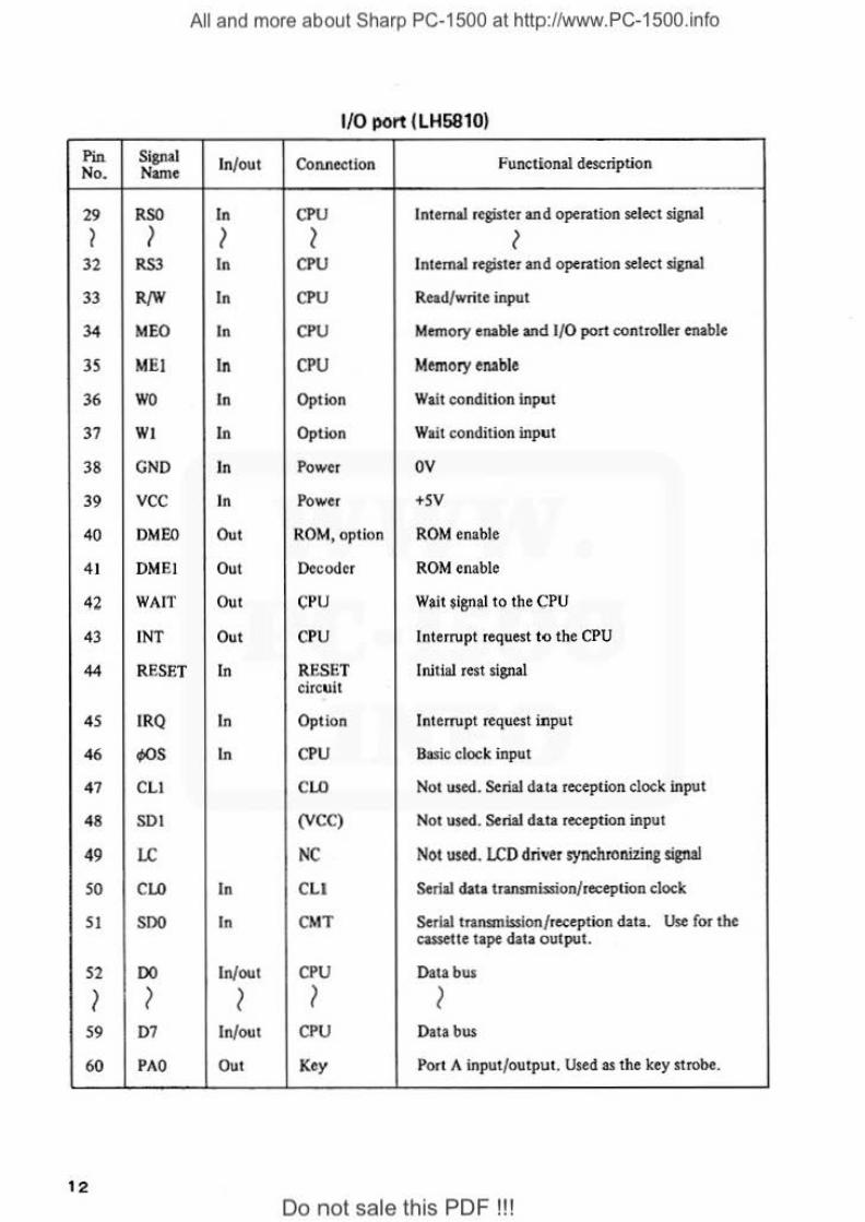
All and more about Sharp PC-1500 at http://www.PC-1500.info
1/0 port {LH5810)
Pin Signal In/out Connection Functional description No. Name
29 RSO In CPU Internal register and operation select signal
? ? ? i ~ 32 RS3 In CPU Internal register and operation select signal
33 R/W In CPU Read/ write input
34 MEO In CPU Memory enable and 1/0 port controller enable
35 MEI In CPU Memory enable
36 WO In Option Wait condition input
37 WI In Option Wait condition input
38 GND In Power OV
39 VCC In Power +SV
40 DMEO Out ROM, option ROM enable
41 DM EI Out Decoder ROM enable
42 WAIT Out CPU Wait $ignal to the CPU
43 INT Out CPU Interrupt request to the CPU
44 RESF.T In RESET Initial rest signal circuit
45 IRQ In Option Interrupt request input
46 </>OS In CPU Basic clock input
47 CLI CLO Not used. Serial data reception clock input
48 SDI (VCC) Not used. Serial data reception input
49 LC NC Not used. LCD driver synchronizing signal
50 CLO lo CLl Serial data transmission/reception clock
51 SDO In CMT Serial transmission/ reception data. cassette tape data output.
Use for the
52 DO In/out CPU Data bus
> ? ? ? ? 59 D7 In/out CPU Data bus
60 PAO Out Key Port A input/output. Used as the key strobe.
12
Do not sale this PDF!!!

All and more about Sharp PC-1500 at http://www.PC-1500.info
Read/write timings for 1/0 port
Yl'Al1'* __ _
D0-7 -----<====>-(a) Data read from 1/0 port
MREQ'i: _ _,
R1w-----. ~---~
WAIT*--~
vo-1 --c=======>-(b) Data wire to 1/0 port
Do not sale this PDF !!!
NOTE: Clock q, is furnished to the ¢OS input of the I/O port. MREQ• is an inversion of MREQ of Z-80 and furnished to the MEO of the I/O port. WAIT• is an inversion of WAIT of the I/0 port and furnished to the WAIT input of Z-80.
13

All and more about Sharp PC-1500 at http://www.PC-1500.info
4. CIRCUIT DESCRIPTION1
4-1 .. Chip Select Circuit
c p
u
I/o p 0 DM£1
DllEO R T MEO
MEI
ADS TC40Hl89F TC40Hl·38F
VGG
so To RAMS (TC551? AF)
S I
52 Tu MOOJle Unil
sa
S7 Y4
Y5
Vss Vss n SG
vee WEX Th 1/0 Port
V2 To OiSplay chip 1.3
L......f---Q=va To Display <;l1ip2.4
'-- --- - ---+To RAllj , 2(TC,:~~14r)
'------- ----- - ----- -+ To VO PORT( LH5810)
'--+To R0ll(CS613 128F)
'---- ----------- - ---•To MOOul lhi t
'----- ---- ----- - -----+To Mcdvl lhit
tt.tou1i• Internal logic Truth Table VO
A
Input ENA.BL! Sl>L1$CT Output
Vi •• •1£8 A • c ~ 2'.1 Y! VJ ... "' "' Y'1 L '" " " "' .. H H II II II H II "
$F.LECT Y2 • " ... ( · 0 <:> II II II II " II II " ... .. " (,;- Ii:. ~ II II II H II II II II
Vi II L L L L L I. " " H II II II II
c Yi
II L L II L L II L II II II II " II
II L I. L " L " " L H H " " II
{CIA "' £NA8\.f. Gtll
C l VJ
" L L " H L !I II " L " " " II
" L L I . L H II " II H L H H H
H L L II L II II II " II II L II H
" L L L H II II II H II II H L H
II L L II H H H II H H " II " L
Y'i
'" Do not sale this PDF !!!

B
A
0
All and more about Sharp PC-1500 at http://www.PC-1500.info
Truth Table
Input
Er.ISLE SELECT Output
G A B YO Yf Y2 YT YO
Yi H * * H H H H
L L L L H H H Y2 L H L H L H H
L L H H H L H
L H H H H H L Y3
l*= Irrelevant
- -• Selection of I YO - I Y3 by the decoder IC (TC40H l 39H) is done when the gate signal (GI) input BFO is low_
YO With low state of AD 14 and AD IS. the YO output becomes low to select the system ( !YO) ROM area of the module unit. (0000- 3FFF address setup)
YI With high state of ADl4 and low state of ADl5, the YI output becomes low to select (IYI) the gate (G2A) of the IC (TC40HB8F). (4000- 7FFF address setup)
Y2 Wi th low state of AD14 and high state of AD15, the Y2 output becomes low to select (IY2) the expansion ROM area of the module unlt. (8000- BFFF address setup)
Y3 With high state of AD14 and AD15, the Y3 output becomes low to select the system (IY3) program ROM (CS-613128F) and the 1/0 port (LH5811). (COOO - FFFF address
setup)
• Selection of SO - S7 by the decoder IC (TC40Hl 38F) is done when the gate signal input MEO (GI) is high, YI (G2) low, and G2B is low {which is normally low).
SO With all of AD II, AD 12, and AD B in low state, SO goes to the low state and selects the (YO) RAM3 (TC5517AF). (4000-47FF address setup)
SI With high state of ADI I and low· state of AD12 and AD13, SI goes to the low state to (Y I) select the option user RAM area . (4800-49FF address setup)
S2 With low state of AD 11 and high state of AD 12 and low state of AD 13, S2 goes to the (Y2) low state to select the option RAM area. (5000 - 57FF address se·tup)
S3 With high state of ADii and ADl2 and low state of ADl 3, S3 goes to the low state to (Y3) select the option user RAM area. (6000- 67FF address setup)
S6 With low state of AD 11 and high state of AD 12 and AD 13, S6 goes to the low state to (Y6) receive the interrupt input from an option into the 1{0 part. (1000 - 77FF address
setup)
S7 With all of AD 11, AD 12, and AD 13 in high state, S7 goes to the low state to select the (Y7) system memory RAMI and 2 ('TC5514P). (7800 - 7FPF addres setup) RAM! and
RAM2 are 4·bit RAMs, independently used to assume low order and high order bits to comprise one byte with a pair of 4 bits each.
• Selection of 2Y2 and 2Y3 by the decoder IC (TC40Hl~is done when the gate C>f2G becomes active with the selection of the TC40H J38F output, S6 (Y6).
2Y2 With low state of ADS and high st ate of DMEO, the 2Y2 output goes to the low state so (V2) that the NAND gate output V2 is turned hlgh to select the display chip I and 3.
2Y3 Wi th high state of AD8 and DMEO .• the 2Y3 output goes to the· low state so that the (V3) NANO gate out V3 is turned high to select the display chip 2 and 4.
• Display chip (SC882G) is a 4·bit RAM, comprised of one byte of data wit11 4 low order bits and 4 high order bits of data, so that even the chip select signals are used in pair of chip I with chip 3 and chip 2 with chip 4.
15 Do not sale this PDF !!!

All and more about Sharp PC-1500 at http://www.PC-1500.info
2) Buzzer cir cu it
CJ.IT OUT 10 I SDO 1 \6 PC6 l:-,-.--~<1--...219 L..) p 4 O PB2~1~1 --+--k1-__. R T
CMT IN
Vee
BUZZER a Ott---.
The control signal CMT OUT is setnt out from the pin SDO of lhe 1/0 port wich sounds the buzzer in oombination with the low state of either the programmed output from the 1/0 port or CMT IN
sent from the cassette tape deck.
3) RAM R/W signal circuit
R/W RAJ.II
R/W • CPU 1-AD~l~O:.._l>l--_....,/W :__,-
F:..:.:..--f:>t---t
6.6KO TC5614PX2 pcs
4) ON key double action preventive circuit
16
Vee
OAP 202
560KO
BF I - -W"l'-_.- +-"-15 ~4C........._-.Q I /0 PORT
SFI --""
TC50HOOI
~""'-asr~·~39PF
...-----~
PS7 ---'
P87
This circuit prevents writing if ADIO is in high state during the write mode (when R/W is low). This is to prevent wrong operation when a specific key, [!] or [I] is pushed without performing "NEW 0 ENTER" after battery replacement.
This circuit consists of the Schmitt circuit that prevents the possibility of setting the input flag of the LH5B 11 1/0 porl which depend~ on how the ON key is pushed.
Do not sale this PDF !!!

All and more about Sharp PC-1500 at http://www.PC-1500.info
5) Timer/counter circuit
-.... 0 ..., 0
"' '"l
r = (ft
"" --
Pin No.
I
2
3
4
5
PCS C2
PC4 C l
PC3 CO
PC 1 t--- -+-1 STB
Reset
ILSBI
" ..., 0 -., ., 0 > (")
Yoo
XTALI-----~
~ITt---....J lrJ s2.1ssKHz liTAL 0 ~ :!:: 1. Ou~lino
>--~ "[__J As shown in the left, ,;. the µPD! 990AC is used
for the time keeping IC to count hour/minute/ secondfmonth/day.
2. Main function of µPD1990AC
Time data is in the BCD form and i;;judged by means of comparison. However, day of week is not used with this chip and hour is represented by 24·hour system.
IMSBI DIN
9 4 3 2 2 5 2 B --Second$ Minutes Hours Day Week Monti\
4 4 I 4
Bits Bits 4 I 4
Bits Bits 4 I 4
Bits Bits
4 4
Bits Bits Bits
Signal In/out Description name
C2 In Mode select signal C2=0
C i In Mode select signal Cl co Mode Data In/out mode
co In Mode select signal 0 0 0 Resister hold
0 1 I Registered shirt
I 0 2 Time set
I 1 3 Time read
STB In Strobe. Command is latched by the strobe STB.
cs In Chip select: disables CLK and STB input and DAT A OUT output by the CS input. All input/output are invalid unless CS is high.
STB "\_ J Internal STB (command latch clock) cs ./
~
CLK ] ) Internal CLK (40-bit serial clock)
] "\_ Internal OE (gate input of DAT OUT) OE ../
17
Do not sale this PDF !!!

All and more about Sharp PC-1500 at http://www.PC-1500.info
6 DATA IN In Data input signal (40-bit serial data)
7 CND In ov 8 CLK Jn 40-lbit shift register clock (Data input/output is carried out in
synchronization with CLK.
9 DATA Out Data output signal (40-bit serial data) OUT
10 TP Out Timer pulse output: to CO, CI, C2 during command assignment.
11 OUT In Output enable: input to control the output of DATA OUT. ENABLE
12 XTAL In Basic clock, 32.768KHz
13 XTAL In Same the above
14 YDD In Source power input, connected to VGG (4.7V).
6) Power supply circuit
The power supply is lllCOrporated in 3 Single resin molded IC that consists of the stabilizer circuit, temperature compensation circuit, and bleeder circuit.
18
VBATU----,
HI-MIC
18
ri>t-+-14"°"1'""""2'SB7_Jc0,.__--:2:.:;:SB77.9~-~~~~f-<o------O ' ' Vee
ADAPTER Jack
I SS98
--:"UM-8 X4
2SCl628
9
SFO
7
6
VR
8
--- ovA 3
2 Vi.r
+---OVs
'--<>-..... -----1--------<>--+-----.--------+--6..J .._...._ ____ --OVotsP 5 2SJ84 4
GNO
Supply voltage: I .SY x 4 = 7Y ±0.05V VCG: 4.7V VCC: 4.7V !0.02V VDISP: 3.7V ±0.0IY (In the case of 2S°C)
Do not sale this PDF !!!

All and more about Sharp PC-1500 at http://www.PC-1500.info
5. STERVICING
1) Measures against irregular condition sR.ll
In a rare case, all keys on the keyboard might become inoperative, including the~ key, when a strong external noise interference is met or when a strong impact is given to the machine body. When such a condition is eji~ptcrd, keep the ALL RESET key pushed for a period of about 15 seconds while .depressing the :~K key.
BRFAK Depressing I ON I key . -.
AU resbt
Use the tip of a ball point pen to push the ALL RESET SW. Do not use the tip of something such as a pencial of which the tip is liable to break. Also, do not use anything with a sharp edge such as a needle up.
Wait for the prompt l"NEW O?: CHECK" to appear on the display, then push I CU NEW 0 I ENTERI. If the prompt " NEW O?: CHECK" does not appear, try the above entry again. Do not use the ALL RESET switch except for the above operation, or destruction of the. program, data, and reserve contents will occur.
2) How to replace FPC (Flexible Printed Cable)
To replace the f PC that connects the Key PWB with the Operation PWB, the following procedure should be used.
2-1. Removal
Saldering
Do not sale this PDF !!!
Since the Operation PWB is connected with the FPC by means of th.e crip metal, the Key PWB is disconnected from the Operation PWB after removing the crimp metal.
19

2·2. Replacing
20
All and more about Sharp PC-1 500 at http:f/www.PC-1500.info
Lift ing up
Soldtrin,g I ron
The Key PWB is connected with the FPC by soldering. Peel away the double-tack taipe that fastens Ute FPC with the PWB, then apply the tip of the soldering pencil on the side of the soldered sur· face to remove the FPC, while lifting up the end of the FPC lightly.
(I) Coat the FPC ad PWB with solder with care not to make it uneven.
(2) Temporarily secure the FPC using the double-tack tape.
(3) Match the printed circuit pattern of the PWB with FPC and secure them temporarily . Slide the FPC about I mm backward in this case.
Do not sale this PDF !!!

All and more about Sharp PC-1500 at http://www.PC-1500.info
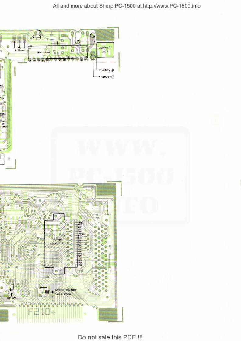
6. PC.1500 KEY & POWER SUPPLY CIRCUIT
v,~,r·r>-----..;•c::•:::••:::•;.;· 'c.' ;:..,' •
Vo:; r-- - - - - - - - -- - --- - -- , ·1 -t:t.r·- --- - .. .., I 13 I ; 1 lli~ l t; I
0710 fl'n9 , 1&:KOj I (-4',.---l>t-_._-<>-1--... .. •
' ;.011rTFlR : J:.-('I<
I I I I I I I 1z~t L
I I WA IMK!
120
L _____ .J
'" ., ----, $?
1 1 Ji l'O I
I I I l_ ..
LTo., .... ,.z ,J, Hi • MI C 12r 1so-'--, ,},(;s-u
A LL WM;rt 1:-. (;so
KF,Y MA1'W I X
l' A()
Do not sale this PDF !!!
I ,., I I I
I L __ J 3 ., I
0.1/'' ' •
"" " I
0.1,.t• ' , 1
I :?SJS-4 ,., ' I ls _________ !,,
• P:\ 1
Vtt
\' "
'" vn
\'<Ji~
tit ' I
21

All and more about Sharp PC-1500 at http://www.PC-1500.info
Do not sale this PDF !!!

Pc-15()~~~-·lgn~-tl~2!$tt2:tJ!fw~1 i;_pjl . into
PC-1500KEY PWB (From the February I 982 Production)
._ __________ _... ................. ._. ..... __________________ _. ____ ___
I Do not sale tn is PDF"T!!

All and more about Sharp PC-1500 at http://www.PC-1500.info
Production)
-----~------ ___________ _..,.
---------- "·o not sale"ihis F>Dr !!1 ___ .,.

PC-NJOOM\B;>rp.iabJJUN!Bar~t~~CQa~~:~~rj::-1 500. info
PC-1500 MAIN PWB (From the February I 982 Production
I L • • L__r-:
Do not sale this PDF !!!

All and more about Sharp PC-1500 at http://www.PC-1500.info
2 Production)
_J
Do not sale this PDF!!!

pc_ 15oo MA 00 a19 .W.8abf f9&~~f~W&a~ttpytwww.PC-1500.info
PC-1500 MAIN P. W. B (From the .July 1982 Production)
. 0 . ' ~ ' ~ !~~·
Do not sale this PDF !!!
All and more about Sharp PC-1500 at http://www.PC-1500.info
Do not sale this PDF !!!

All and more about Sharp PC-1500 at http://www.PC-1500.info
10. LCD SEGMENT & BACK-PLATE SIGNAL
" . . . ' . • '
.l
.. " " " . ' . .
' . : !
' ' ' • • .
)\l\V
! : ' : ! ! . . . ' ' . ' . ' . . . ' . ' ' '
I I >"" . [5
Do not sale this PDF !!!
• · ·~ u1: uuu ...... .,. ~ ,
• t • u 11" 11 1:1:11u u u ... "lhl' .... .
' : : ·' . . .. ~ " " " .. . .
' .
' ' ' : ; ; • .. " " " " • • ' • ' . . ' '
I I I I I ~ ..... I. I '" I ' I ' "" I

J .
J
ut: n11u1• . . .. . . .
All and more about Sharp PC-1500 at http://www.PC-1500.info
If iJ " • .. . . . • • . . 3 0 . . ", .. , l ",, l " "~ .. ~ .. ,l,J"", I
" " " .. " ~ .. " " • ~ • " r. r. " • • " > • . . . • . . . . . . . ' . " " • " .. .. " 1 " r t " " • • • ~ ~ ~ • • . . • . . . • . . . . . . . .
8 cl] •I U ••• I I I
I • I • I• I
Do not sale this PDF !!!
' • . " • • . . l
. " .... o • • I
25

All and more about Sharp PC-1500 at http://www.PC-1500.info
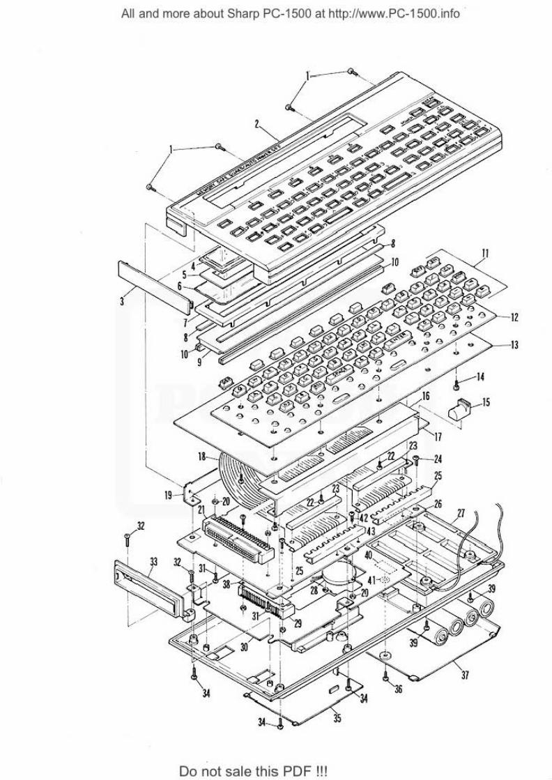
11. PARTS UST & GUIDE
NO. PARTS CODE DESCR I P T I ON "T ll~vl I MARK
PAATS PRCE fW.J< R A14K
1 LX-BZ I I 23CCZZ S C(CW N c A A 2 QUNTG6449CCZZ Cabittet top unit N D A s 3 GFTAAl267CCZZ Connocto( lid N D A c 4 PFi LWl391CCZZ Display f il ter N c A 0
5 PSL DP l 3 2 2CCZZ Display mask N c A c 6 PF i LWl354CCZZ Polarizat ion fi lter N I c A E 7 L ANGK l 437 CCZZ Angla f<>r LCD N c A c 8 l?TPEH I 033CCZZ LCO fix ing tape c A A 9 VVLLF8082GE- 1 LCD N B B A
10 PClUMS 190CCZZ Rubber connec1or- B A F 11· 1 ..J KNBZ 73 1CC01 Koy lop 1 sct/eacl\ IPC N f c A G
11· 2 ..JKNBZ 7 33CC0 1 Key top 1 s01/10PCS N j__£_ A F II · 3 ..JKNBZ 705CC05 Koy !Op 1set/each IPC N c A F il· ( .JJ<NBZ 705CCI O Koy lop 1 set/20PCS N c A F II · 5 ..JKNBZ 705CC06 Key lop 1 se1/20PCS N c A F II-$ ..JKNBZ 705CC07 Key top 1 SC1/20PCS N c A F II • 7 ..JKNBZ 705CC08 Key top 1 se1/lOPCS N c A F
II · S ..J KNBZ 7 3 2CCO I Key !Op 1 set/10PCS N c A F
II· S ..JKNBZ 622CCOI Key !Op 1 set/20PCS N c A E 11 -10 .JKN BZ 515CCIO Key top 1 so1/20PCS N c A F 11-11 .JKNBZ 4 95CCZZ Key top 1se1/30PCS N c A D 11-IZ .JK NBZ 5 15CC I I Key tQP lsc,./20PCS N c A F 11-1; .JKNBZ 5 15CC l 2 Key top 1so</20PCS N c A F 11-14 .JKNBZ 493CC03 Key top 1 set/ 30PCS N c A E 12 P GUMM 389CCZZ Key rubbor N c A L 13 DUNTK6381CCZZ Key PWB unit N E c A 14 LX BZI060CCZZ Scr ew N c A A 15 Q..J AKCI003CCZZ Jack sockdet c A D
16 PZETL l427CCZZ Insulato r N c A A 17 LANGT l 439CCZZ An~1lc 8 N c A c 18 QPWBM2027CCZZ FPC N c A ,_ 19 LANGTl438CCZZ Angle A N c A 0 20 :XNE5D20- 16000 Nu1 c A A 21 QCNCW l293CCZZ Conncc~or 60pirl N c A y
22 :XBBSD20P06000- Screw c A A
23 L FiX- 1 I 16CCZZ F ixing c ushion N c A B -24 .XU BSD20P0 5 0 0 0 Scr ew c A A 25 L ANGK 1221CCZZ Fixing ;.lnnle I c A D
26 IDUNTK6382CCZZ Calcula1ion PWS N E ~41 27 CCABA2595CCO I Bottom cabinet {w ith battery termina}L N D A N_-j 28 IRA LMB 1006CCZZ Buzzer a A H
29 QCNCW l 294CCZZ C()fUl(X~ '(()C 40p i 1'l N c A x 30 PSL OC l 32 1CCZZ Soald l'lale N c A F 31 XBBSD20P08000 Screw c A A 32 XUBSD20P05000 Screw c A A 33 GWA KP 041CCZZ Connector annle N c A F 34 LX BZ I I 5CCZZ Screw N c A A
35 GFTAU 268CCZZ Lid for modulo N L> A c 36 L X BZ 124CCZZ Screw N c A B 37 GFTAB 266CCZZ Lid f(lr ba n ery N D A c 38 PS PA P 207CCZZ Conncc :or spacer N c A A
39 LX- BZ I 14CCZZ Sc rew N c A A 40 LF i X- 126CCZZ F ixinn plate N c ~4-1 41 LX NZ 0 12 CCZZ Nu1 c A A 42 L X-BZ I 13CCZZ Scr ew N c A A
43 PS LOP 334CCZZ Mosk N c A ·~ ~ LX- BZ I I 6CCZZ Screw c A A
PC - 1500- ID
Do not sale this PDF !!!

All and more about Sharp PC-1500 at http://www.PC-1500.info
NO. PARTS CODE DES CRIPT I ON N( W PARTS fl!C£ PA~ Mti.FIK RANK
RC-CZl02 1CCNI Capacitot 0. lµF N c A B RC- CZI023CCNI Capacitor tOOPF c A B RC- CZ 104 1CCN I Capacitor 15 PF N c A B RC-CZ I042CCNI Capacitor 30PF N c A B RC- EZI05ACC I H Capacitor 50V/ lµF c A B RC- EZ227ACCIA Capaci tor 10V/ 220µF c A c RCRSP1 036CCZZ Crystal 32.768KHz 8 A H RCRSZI 0 38CCZZ Crystal 2.6MHz N 8 A E RH-DZl005CCN I Diode [)AP202 N 8 A c RH-DZI008CCN I Oioda [)AN202 N 8 A c RVR- MB5 10QCZZ Valiablc tcsistor 250Kohm c A E RVR- Ml3SB50QC Valiable resistor 220Kohm N c A 0 SPAKA67 60CCZZ PackinQ cushion N 0 A 0 SPAKA688 1CCZ Z Packing cushion N 0 A H SPAKC6642CCZZ Packing case (U.S.A) N 0 A K S P AKC676 1CCZZ Packing case N 0 A F TCAUH I I 8 I CCZZ Caution label for modul 0 A A T iNSE3434CCZZ lnstructior' book (lJ.S.A) N 0 A x T iNSE3483CCZZ Instruct ion book (Others English) N 0 A x T iNSG3517CCZZ Instruct ion book (Germany) N 0 T iNSM348 1CC Z Z Instruction book (E. F. G, S) N 0 lrMANE I 022CCZZ Program l ibraty (English) N 0 A z T MANGl023CCZZ Pr()!Jram library (Germany) N 0 UBAGCl290CCZZ Soft case N 0 A R VHDDSl566L.l-I Diode 1:srnssL1 B A D VHO I SS98// / - I Diode N 8 A 0 V HHl 54KD- 5/- I Thermist or 150Kohm B A c
j_ VH i EHM7 I SL 70N I. C. (Power regurator) N 8 A T _!_ VH i HM6 11 6 // - C I 1. C. (HM61 16) N B B H
I VHiLH580 1// - I l . S. I . (LH5801) N 8 8 K VH i LH58 I I / / - I L . S.I. (LH5811 or 5810) N 8 A z VHiSC6 13 128FN L . S. I. (SC613128) N 8 I 8 H VH i SC882G // - I L . S. I. (SC882G) B l A w VH i TC40HOOOFN I. C. (TC40HOOO) N B A G VHiTC40Hl38FN I. C. (TC4CH138) N B _L A Q VHiTC40H l 39FN I. C. (TC40H1 39) N 8 [ A Q VHiTC50HOOIFN I. C. (TC50H001) N B I A H
V HiTC55 14P/-C I. C. (TC5514P) I N B A u I VHiUPOl990 ACC I. C. (µP01 990A} B A T
VRS- T P2BDIOOJ Resistor 1/BW 100ohm c A A
VRS- T P280 10 2J ReS1stor 1/BW 1Kohm c I A A VRS- T P280103J Resistor 1/BW 10Kohm c J. A ~A" VRS- T P2BD I 04J Resistor 1/BW 100Kohm c i A A VRS- TP2B0333J Resistor 1/BW 33Kohrn c T A A --VRS- TP280473J l Resistor 1/SW 47Kohm c A A VRS-TP280 562J Resistor 1/flW 5.6Kohm c A A VRS- TP2BD563J Resist of 1/ SW 56Kohm C A A VRS- TP2BD564,J Resistor- 1/8W 560Koh:n - ·1--C A A VS2SC2412-/-I Transis to1 2SC2412 ' c A c L PLTP I OSOCCZZ Tcnplnte I N ,_ I 0 A 0
- -!- ' ~ L
I J. PC- 1500-~
Do not sale this PDF !!!
All and . ww.PC-1500. info . more about Shar P PC-1500 at http·//w
D . o not sale th' IS PDF Ill ...

> >-12
- 13
9 )
All and more about Sharp PC-1500 at http://www.PC-1500.info
..
Do not sale this PDF !!!

I • • ' •
1:1-ti:;ii: ...... .. , '· +E
Ll -:, Ir.==~~ .. ·~j I
it .,~·~~ ~· r .~ ,...:. .. ~
I I I
~~= · r l~ , . . . . • •• " I '.
i r.._.
. ' o not sale this PDF !!!
. ' .,
-. •
• •I ..
I . .. . . . ...
: : : . . . -. -... - . '
: . '1''i I . . • • I I I
"
r , .. : c'"' : 11 : ; .. t
' I