sigex lab manual.v1.1
TRANSCRIPT

ETT-311 SIGEx
Lab Manual Signals & Systems Experiments with Emona SIGEx
Volume 1
- S A M P L E M A N U A L -

Signals & Systems Experiments with Emona SIGEx
SAMPLE MANUAL
Volume S1 - Fundamentals of Signals & Systems
Authors: Robert Radzyner PhD
Carlo Manfredini B.E., B.F.A.
Editor: Carlo Manfredini
Issue Number: 1.1 SAMPLE Manual
Published by:
Emona Instruments Pty Ltd,
78 Parramatta Road
Camperdown NSW 2050
AUSTRALIA.
web: www.emona-tims.com
telephone: +61-2-9519-3933
fax: +61-2-9550-1378
Copyright © 2011 Emona TIMS Pty Ltd and its related entities.
All rights reserved. No part of this publication may be
reproduced, translated, adapted, modified, edited or distributed
in any form or by any means, including any network or Web
distribution or broadcast for distance learning, or stored in any
database or in any network retrieval system, without the prior
written consent of Emona Instruments Pty Ltd.
For licensing information, please contact Emona TIMS Pty Ltd.
NI, NI ELVIS II/+, NI LabVIEW are registered trademarks of
National instruments Corp.
The TIMS logo is a registered trademark of
Emona TIMS Pty Ltd
Printed in Australia

EMONA SIGEx SAMPLE Lab Manual Volume 1
Contents
Introduction (i)
An introduction to the NI ELVIS II/+ test equipment S1-01
An introduction to the SIGEx experimental add-in board S1-02
SIGEx board circuit modules
NI ELVIS functions
SIGEx Soft Front Panel descriptions
Special signals – characteristics and applications S1-03
Pulse sequence speed throttled by inertia Isolated step response of a system Isolated pulse response of a system Sinewave input
Clipping
Systems: Linear and non-linear S1-04
Conditions for linearity
The VCO as a system A feedback system Testing for additivity Frequency response
Unraveling convolution S1-05
Unit pulse response The superposition sum A rectified sinewave at input
A sinewave input Mystery applications
Integration, correlation & matched filters S1-06
Auto-correlation function of PRBS sequences
Cross-correlation function of PRBS sequences
ACF & matched filtering
Determining impulse response using input/output correlation
Matched filtering using “integrate & dump” circuitry

Exploring complex numbers and exponentials S1-07
Complex numbers and complex functions
Exponential functions
Build a Fourier series analyzer S1-08
Constructing waveforms from sine & cosine
Computing Fourier coefficient
Build a manually swept spectrum analyzer
Analyzing a square wave
Spectrum analysis of various signal types S1-09
Spectrum of impulse trains
Spectrum of filtered impulse trains Duty cycle & sampling Sync pulse train Spectrum of PN sequences Analog noise generation (AWGN) Non-linear processes
Time domain analysis of an RC circuit S1-10
Step response of the RC
Impulse response of the RC
Exponential pulse response of the RC
Synthesising transfer functions
Poles and zeros in the Laplace domain S1-11
System with feedback only – allpole
Impulse response of LTIC systems
Feedback and feedforward – poles & zeros
Allpass circuit
Critical damping & maximal flatness
Sampling and Aliasing S1-12
Through the time domain – PAM, Sample & Hold
Through the frequency domain
Aliasing and the Nyquist rate
Multi-frequency impulse spectrum
Uses of undersampling in Software Defined Radio
Getting started with analog-digital conversion S1-13
PCM encoding & quantization
PCM decoding & reconstruction
Frame synchronisation & quantization noise

Discrete-time filters with FIR systems S1-14
Graphical plotting of response from poles & zeros
Notch filter creation using two-delay FIR
Poles and zeros in the z plane with IIR systems S1-15
Relating roots to coefficients in the quadratic polynomial
IIR without feedforward – a second order resonator
IIR with feedforward – second order filters
Viewing spectrum with broadband noise & FFT
Dynamically varying the poles & zeros
Using the “Digital Filter Design” toolkit
Discrete-time filters – practical applications S1-16
Dynamic range at internal nodes
Transposed Direct form 2 IIR
Implementations with high sampling rates
Appendix A: SIGEx Lab to Textbook chapter table S1-A
Appendix B: Quickstart guide to using SIGEx S1-B
References


Introduction This experiment manual is designed to provide a practical “hands-on”, experiential, lab-based
component to the theoretical work presented in lectures on the topics typically covered in
introductory “Signals and Systems” courses for engineering students.
Whilst it is predominantly focused on all electrical engineering students, this material is not
exclusively for electrical engineers. With an understanding of differential equations, algebra of
complex numbers and basic circuit theory, engineering students in general can reinforce their
understanding of these important foundational principles through practical laboratory course work
where they see the “math come alive” in real circuit based signals. This provides a foundation for
further study of communications, control, and systems engineering in general.
Students take responsibility for the construction of the experiments and in so doing learn from their
mistakes and consolidate their knowledge of the underpinning theory, which at times is particularly
abstract and hard to grasp for these early engineering students. They are not constrained by the
software and need to be systematic in debugging their own systems when results do not meet their
expectations.
The common reaction of early students when confronted with “complex analysis” is one of confusion
and regression to “rote-learning” in order to survive the examination process. This manual has as its
predominant aim to create real, “hands-on” implementation of the theory, in such a way that the
student can directly articulate and connect the mathematical abstractions with real world
implementations. It is a journey of personal discovery where the motto is “why is it so ?”
The use of “modeling” is the fundamental tool in this, and other NI ELVIS-based EMONA boards (such
as DATEx, FOTEx and HELEx), and it has been shown that experimenting with scaled models of real
world systems allows students early-on to get a tangible “feel” for principles that they may later
utilize in real world commercial workplace environments. As well, students tend to “believe” results
from “real hardware” rather than from software simulations, and this supports their “learning by
doing”.
The authors sincerely hope that students using this equipment and guided by this manual will complete
with a sense that complex numbers and systems analysis “makes sense” and is somehow more “real” and
applicable to real world problems. In this way they may successfully use these principles in solutions to
future problems they will encounter.
Carlo Manfredini
Sydney, January 2011


© Emona Instruments Experiment 1 – An introduction to the NI ELVIS II/+ test equipment V1.0 1-2
Experiment 1 – An introduction to the NI ELVIS II/+ laboratory
equipment
Preliminary discussion The digital multimeter and oscilloscope are probably the two most used pieces of test equipment
in the electronics industry. The bulk of measurements needed to test and/or repair electronics
systems can be performed with just these two devices.
At the same time, there would be very few electronics
laboratories or workshops that don’t also have a DC Power
Supply and Function Generator. As well as generating DC
test voltages, the power supply can be used to power the
equipment under test. The function generator is used to
provide a variety of AC test signals.
Importantly, NI ELVIS II has these four essential pieces of
laboratory equipment in one unit (and others). However,
instead of each having its own digital readout or display (like
the equipment pictured), NI ELVIS II sends the information
via USB to a personal computer where the measurements are displayed on one screen.
On the computer, the NI ELVIS II devices are called “virtual instruments”. However, don’t let
the term mislead you. The digital multimeter and scope are real measuring devices, not software
simulations. Similarly, the DC power supply and function generator output real voltages.
As well as the instruments mentioned above, the NI ELVIS II has available eight analogue
inputs and two analog outputs which can be controlled and written to by our LabVIEW program
and the input readings processed and displayed on screen. This allows for the creation of many
more custom "virtual instruments" which may be required in a particular experimental setup.
The experiments in this manual make use of several of the available analogue inputs as well as
several digital inputs and outputs which, in conjunction with the SIGEx board, are able to
implement two groups of programmable gain amplifiers for use throughout this manual.
Rather than utilising several independent instruments from the NI ELVIS as does the other
EMONA plug-in accessory boards (such as EMONA DATEx Telecoms-Trainer and the EMONA
FOTEx Fiber optics trainer), these instruments are all merged into one full-screen virtual
instrument for the SIGEx board known as the SIGEx Main soft front panel (SFP). With an easy-
to-use tabbed layout, each experiment has its requisite instrumentation grouped within tabs by
experiment.

Experiment 1 – An introduction to the NI ELVIS II/+ test equipment © Emona Instruments 1-3
When an NI ELVIS1 unit is connected to a PC it will automatically run the Instrument Launcher
panel as shown below:
Figure 1: NI ELVIS II/+ Instrument Launcher panel
This panel gives the user access to each individual instrument. Several of these independent
instruments are used by SIGEx experiments. These are the FUNCTIONS GENERATOR (FGEN),
the DYNAMIC SIGNAL ANALYSER (DSA) and at times the SCOPE (Scope).
When using NI ELVIS with the EMONA SIGEx board to conduct signals and systems
experiments the user will run the SIGEx Main SFP VI shown below:
Figure 2: SIGEx Main SFP
1 Throughout this manual, NI ELVIS II & II+ are referred to, however the SIGEx board
and software work equally well on the NI ELVIS I platform, with the NI ELVIS I
FUNCTION GENERATOR used in manual mode ONLY, and NI ELVIS in BYPASS mode.

© Emona Instruments Experiment 1 – An introduction to the NI ELVIS II/+ test equipment V1.0 1-4
There are 19 TABS for use with the experiments in this Volume of the manual.
These instruments take their signals directly from the SIGEx board via the EMONA
ETT-040 Universal Base Board, into the ELVISmx circuitry, and after processing by LabVIEW
are displayed on screen as required.
The combination of the LabVIEW programmability of the NI ELVIS unit as well as the numerous
analog and digital inputs and outputs available make it convenient to create customised
instrumentation for use in real world hands-on experimentation. The EMONA SIGEx board is a
good example of this integration of available hardware and the software control.


© Emona Instruments Experiment 2 – An introduction to the SIGEx experimental add-in board V1.0 2-2
Experiment 2 – An introduction to the EMONA SIGEx
experimental add-in board for NI ELVIS
Preliminary discussion The experiments possible with the EMONA SIGEx board bring together worlds of
mathematical theory and practical implementation. We are able to explore, in a hands-on
manner, the representation of physical processes by mathematical models and test and measure
the benefits and limitations of such models. We explore the complementarity of the time and
frequency domains and practice thinking and theorizing in both. Through measurements,
calculations and observations we are able to consolidate our understanding of these domains.
The SIGEx board customizes the instrumentation available on the NI ELVIS to create
experiment-specific instruments which can be used to create many different circuit structures.
As well, the ability to programmatically control, measure and automate our measurements using
LabVIEW bring us closer to real-world practices of system control and monitoring.
Although the principles of being studied date back several centuries their application in real
world devices is continually being explored and implemented. The instrumentation used has
changed substantially however the rigorous nature of the mathematical process remains the
same and is a skill which is best learned in a hands-on manner.
By implementing the many mathematical model and theorems in real hands-on circuit based
experiments, the student reinforces and actualizes their understanding of these principles to
create a solid foundation for future learning.
An important skill for the engineer and scientist is the ability to take rigorous and precise
measurements, often repetitively, in order to study the phenomena at hand. The EMONA SIGEx
Signals & Systems Experimenter (ETT-311) provides an abundance of opportunities to learn and
practice experimental methodology in a variety of related topics which are common ground for
engineering students of several disciplines.

Experiment 2 – An introduction to the SIGEx experimental add-in board © Emona Instruments 2-3
The experiment For this experiment you will familiarize yourself with the various instruments available on the
SIGEx board and how they are used.
It should take you about 10 minutes to read this experiment and explore these functions.
Pre-requisites:
You should have completed the introductory chapter 1 so that you’re familiar with the equipment
setup and capabilities.
Equipment
� PC with LabVIEW 2009 (or higher) & “Digital Filter Design” toolkit installed
� NI ELVIS 2 or 2+ and USB cable to suit
� EMONA SIGEx Signal & Systems add-on board
� Assorted patch leads
� Two BNC – 2mm leads

© Emona Instruments Experiment 2 – An introduction to the SIGEx experimental add-in board V1.0 2-4
Procedure
Part A – Setting up the NI ELVIS/SIGEx bundle
1. Turn off the NI ELVIS unit and its Prototyping Board switch.
2. Plug the SIGEx board into the NI ELVIS unit.
Note: This may already have been done for you.
3. Connect the NI ELVIS to the PC using the USB cable.
4. Turn on the PC (if not on already) and wait for it to fully boot up (so that it’s ready to
connect to external USB devices).
5. Turn on the NI ELVIS unit but not the Prototyping Board switch yet. You should observe
the USB light turn on (top right corner of ELVIS unit).The PC may make a sound to indicate that
the ELVIS unit has been detected if the speakers are activated.
6. Turn on the NI ELVIS Prototyping Board switch to power the SIGEx board. Check that
all three power LEDs are on. If not call the instructor for assistance.
7. Launch the SIGEx Main VI.
8. When you’re asked to select a device number, enter the number that corresponds with
the NI ELVIS that you’re using.
9. You’re now ready to work with the NI ELVIS/SIGEx bundle.
Note: To stop the SIGEx VI when you’ve finished the experiment, it’s preferable to use the
STOP button on the SIGEx SFP itself rather than the LabVIEW window STOP button at the
top of the window. This will allow the program to conduct an orderly shutdown and close the
various DAQmx channels it has opened.
Ask the instructor to check
your work before continuing.

Experiment 2 – An introduction to the SIGEx experimental add-in board © Emona Instruments 2-5
EMONA SIGEx board overview
The SIGEx board is a collection of independent circuit blocks which each implement a single
simple function. No one block is a complete experiment, however several blocks together can
implement a wide variety of different experiments. The block inputs and outputs are patched
together with 2 mm patching leads according to the block diagram as documented in this Lab
Manual or from the many texts available on this topic.
EMONA SIGEx board layout
This chapter discusses the functionality of each module briefly and further details such as
specifications are contained in the EMONA SIGEx User Manual.
NI ELVIS II/ SIGEx bundle

© Emona Instruments Experiment 2 – An introduction to the SIGEx experimental add-in board V1.0 2-6
SIGEX board circuit modules
Sequence Generator
Limiter
RC Network
Rectifier
The SEQUENCE GENERATOR provides a source of periodic data
streams which are output as 5V logic and bipolar level signals.
DIP switches allow the selection of 4 different streams.
A periodic SYNC pulse is output once per frame.
The module is clocked by a single input logic level clock. This will
typically come from the PULSE GENERATOR or FUNCTION
GENERATOR/SYNC outputs.
The state of the DIP switches at any time is displayed on the SIGEx
SFP along with a description.
The LIMITER amplifies an incoming signal with DIP switch selectable
gain levels and to a fixed level, creating an amplitude limited output
signal.
It is typically used with bipolar analog sinusoidal signals or bipolar line
coded data streams.
The RC NETWORK provides R and C elements which can be arranged as
either an RC circuit which acts as a LPF, or as a HPF.
The elements are floating and one end needs to be connected to GND.
The Rectifier provides half wave rectification of an incoming signal with
a non ideal diode component which has a forward voltage drop.
This is typically used with sinusoidal signals.

Experiment 2 – An introduction to the SIGEx experimental add-in board © Emona Instruments 2-7
Multiplier
Integrate & Dump/Hold
Baseband Low Pass Filter
PCM Encoder
PCM Decoder
The Multiplier provides four quadrant multiplication of two analog input
signals. Its overall gain is approximately unity and it is used to model
any multiplication process that may occur in a block diagram.
Both Integrate and Dump as well as Integrate and Hold is available in
this circuit block. Usually clocked by the bit clock of an incoming
sequence, it is used to integrate over a single period of a waveform in
correlation and filtering functions.
This LPF has a 4th order Butterworth response and serves both as a
“system under investigation” and for general filtering functions.
This module implements PCM encoding of a single analog signal. It
outputs an 8 bit frame along with a periodic Frame Sync pulse.
It can be used with both DC signals as well as sinusoids and serves to
allow specific investigation of the encoding process.
It has a maximum sampling rate of 2.5ksps ( 20kbps PCM data stream),
and so can be used with signal frequencies below the Nyquist limit of
1.25kHz.
This module implements PCM decoding of an 8 bit PCM digital data
stream from the PCM Encoder.
The Frame Sync is necessary to achieve synchronization and there is no
reconstruction filter on the output to allow investigation of quantization
issues.

© Emona Instruments Experiment 2 – An introduction to the SIGEx experimental add-in board V1.0 2-8
Tuneable Low Pass Filter
Integrators
Unit delays with Sample & Hold
This module is an adjustable LPF. It implements a 8th order Elliptic
filter with an adjustable corner frequency. The output signal level is
also adjustable, and it can accept analog and TTL level digital signals.
There is no anti-aliasing filter on the input so users need to be aware of
the bandwidth of their incoming signal.
These 3 independent circuits are simple integrator circuits with a common DIP-switch-
selectable integration rate. They are used for continuous time integration ( unlike the
Integrate & Dump/Hold unit which operates over a single period only.)
They are used in Laplace domain experiments.
The DIP switch settings is displayed in the SIGEx SFP along with the approximate integration
rate.
The Sample & Hold is an analog sampler circuit which holds the sampled value for a single period
of the incoming TTL level clock signal. The unit delays are similar in that they hold the incoming
analog value at their input for a single clock period.
All 4 units share a common clock signal.

Experiment 2 – An introduction to the SIGEx experimental add-in board © Emona Instruments 2-9
Triple and dual input adders
There are 3 adder sections. Two identical triple input adder sections and a dual input adder.
The triple input adders, a & b, have adjustable gains. These gains are adjusted via the SIGEx
SFP and are typically used to implement the taps in feedback and feedforward systems.
The dual input adder has unity gain and is used for general purpose addition.
The GAIN ADJUST knob is read by the SIGEx SFP software and can be used to manually
adjust adder gains.

© Emona Instruments Experiment 2 – An introduction to the SIGEx experimental add-in board V1.0 2-10
NI ELVIS functions blocks available on the SIGEx board
Pulse generator / Digital out
Function generator
Analog out
This module makes available the built in Pulse Generator from NI ELVIS
which has a very broad range of frequency and duty cycle control. This
is controlled from the SIGEx SFP and is usually used to provide digital
clock signals to experiments.
D-OUT-0 is a single digital output line which is available but currently
unused in experiments.
This module makes available the built in Function Generator from NI
ELVIS which is a multifunction generator, with variable signal types,
variable amplitude and variable frequency. It is controlled via its own
instrument panel which available from the NI ELVIS Instrument
Launcher panel.
This module makes available the built in dual analog outputs from the
DACs.
These outputs are controlled from various SIGEx experiment TABs and
can be modified to create any periodic waveforms required.
Experiment 2 – An introduction to the SIGEx experimental add-in board © Emona Instruments 2-11
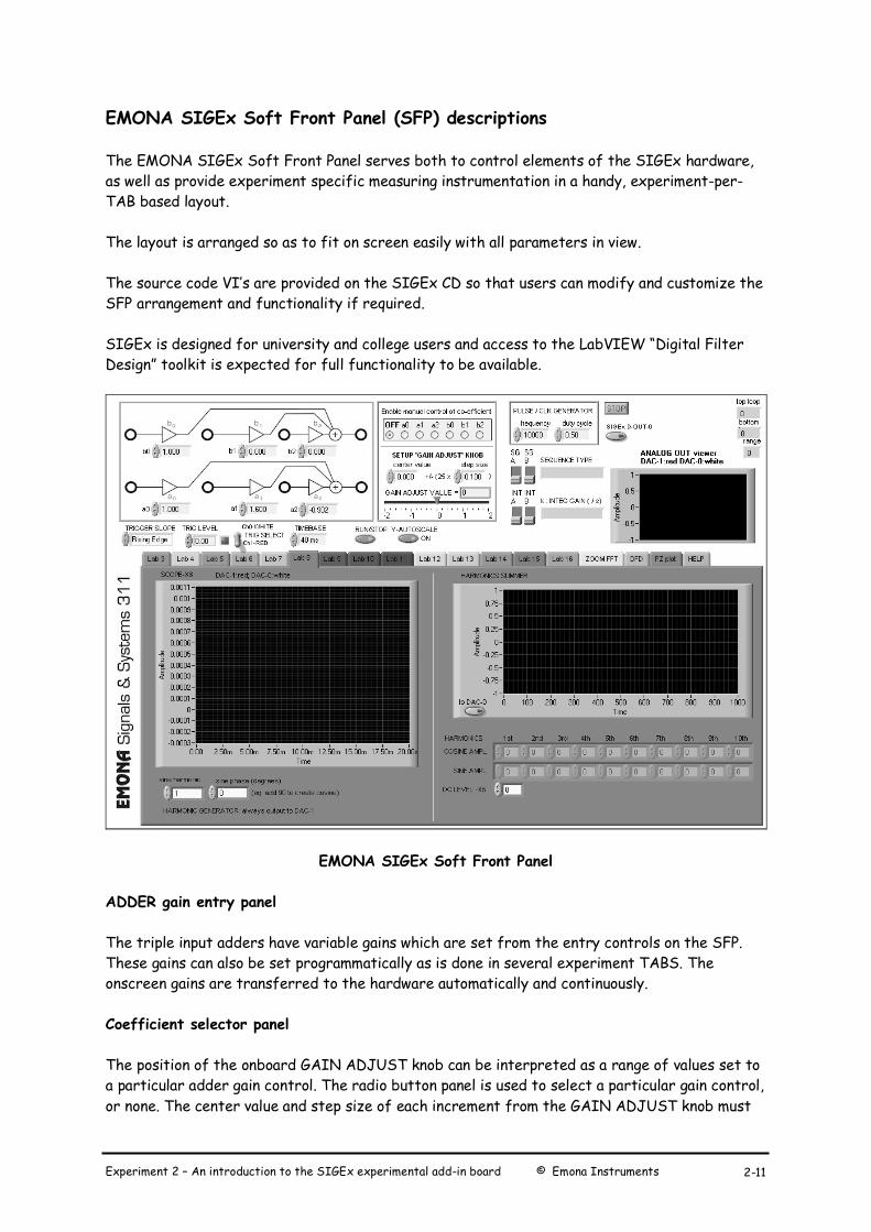
EMONA SIGEx Soft Front Panel (SFP) descriptions
The EMONA SIGEx Soft Front Panel serves both to control elements of the SIGEx hardware,
as well as provide experiment specific measuring instrumentation in a handy, experiment-per-
TAB based layout.
The layout is arranged so as to fit on screen easily with all parameters in view.
The source code VI’s are provided on the SIGEx CD so that users can modify and customize the
SFP arrangement and functionality if required.
SIGEx is designed for university and college users and access to the LabVIEW “Digital Filter
Design” toolkit is expected for full functionality to be available.
EMONA SIGEx Soft Front Panel
ADDER gain entry panel
The triple input adders have variable gains which are set from the entry controls on the SFP.
These gains can also be set programmatically as is done in several experiment TABS. The
onscreen gains are transferred to the hardware automatically and continuously.
Coefficient selector panel
The position of the onboard GAIN ADJUST knob can be interpreted as a range of values set to
a particular adder gain control. The radio button panel is used to select a particular gain control,
or none. The center value and step size of each increment from the GAIN ADJUST knob must

© Emona Instruments Experiment 2 – An introduction to the SIGEx experimental add-in board V1.0 2-12
also be set. This allows either a broad range of values or a narrow focused range of values to be
adjustable via the knob.
Pulse Generator panel
In the panel the frequency and duty cycle of the PULSE GENERATOR block can be set. As well
the spare D-OUT-0 line can be toggled.
SG Sequence type and Integrator Gain readouts
These readouts mimic the selection of the onboard DIP switches and the text briefly describes
the signal type selected for convenience. Details of signals in the SIGEx User Manual.
Analog OUT viewer
This graph indicator displays the actual signal currently being output from the ANALOG OUT
terminals from the DACs. These vary depending on the experiment selected, and this readout is
convenient when SCOPE channels are being used for other signals.
SCOPE Trig level, trig slope, triggered LED, trig select, timebase etc
These controls are for the SFP scopes embedded in various experiment TABs.
Trig level sets the voltage level the trigger looks for. Usually set to 0 or 1 V
Trig slope allows triggering on either the positive or negative edge of a signal.
Triggered LED is ON (green) when a trigger point , as defined above, is detected.
Trig select determines which channel acts as the trigger.
Timebase varies the amount of real signal time to be captured and displayed. Total time
displayed is selectable.
RUN/STOP enables halting of the scope display for close inspection.
Y autoscale ON: enables toggling of the Y axis autoscale function for stable signal viewing with
varying amplitude signals.
This built in scope is a convenient, customized signal display for use in specific experiments.
Spectrum display is also available in certain TABs when required.
Note for ELVIS 2+ users
Due to the independent scope instrumentation available in the ELVIS 2+ it is possible to
simultaneously use the independent scope from the Instrument Launcher panel as well as viewing
the signals in the TAB based scope display.
The Dynamic Signal Analyser (DSA), a spectrum analyser, can also be used, but not at the same
time as the independent scope.

Experiment 2 – An introduction to the SIGEx experimental add-in board © Emona Instruments 2-13
Laboratory Experiment ‘X’ TABS
Each experiment in the SIGEX Lab Manual has its own SFP TAB if required.
Select the TAB as required and the appropriate instrumentation will be displayed. Labs 3 to 18
have TABs available.
Some graphs also have cursors enabled. These are very useful for taking accurate & quick
measurements.
HINT: Right-clicking on a graph will display extra available options you can use. Different
options are available when you right-click while the SFP is not running eg: setting a graph from
linear to log display is done while SFP is not running.
Digital Filter Design TAB
This TAB makes available several of the digital filter design features from the toolkit in one
handy display. The user should select a filter type from which the transfer function will be
calculated. The coefficients from the transfer function are extracted and setup on the SIGEx
hardware as the triple ADDER gains when required by the user. This can be seen on the SFP.
The calculated responses are displayed onscreen.
To view the actual signals and responses from the hardware, switch to a TAB which contains a
scope and FFT, for example the ZOOM FFT TAB, whilst inputting an appropriate source signal.
Note that SIGEx is limited to implementing only up to 2nd order filters. A red “error” LED will
highlight when orders >2 are selected.
© Emona Instruments Experiment 2 – An introduction to the SIGEx experimental add-in board V1.0 2-14
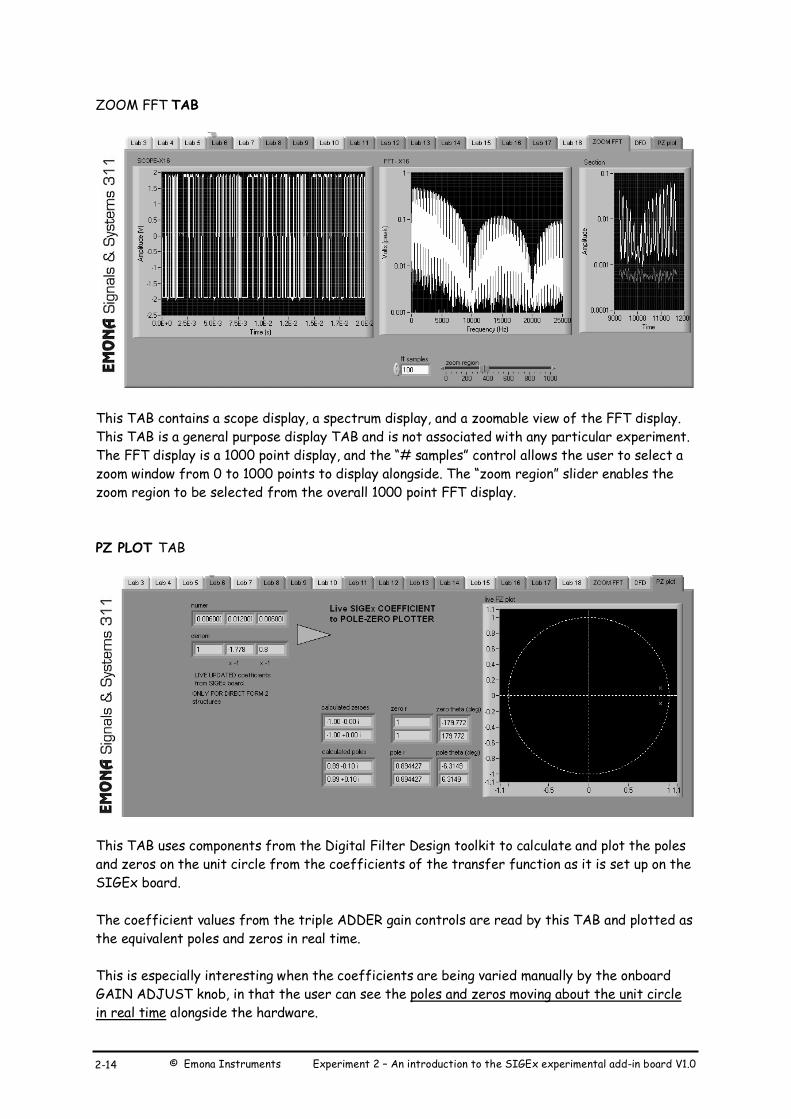
ZOOM FFT TAB
This TAB contains a scope display, a spectrum display, and a zoomable view of the FFT display.
This TAB is a general purpose display TAB and is not associated with any particular experiment.
The FFT display is a 1000 point display, and the “# samples” control allows the user to select a
zoom window from 0 to 1000 points to display alongside. The “zoom region” slider enables the
zoom region to be selected from the overall 1000 point FFT display.
PZ PLOT TAB
This TAB uses components from the Digital Filter Design toolkit to calculate and plot the poles
and zeros on the unit circle from the coefficients of the transfer function as it is set up on the
SIGEx board.
The coefficient values from the triple ADDER gain controls are read by this TAB and plotted as
the equivalent poles and zeros in real time.
This is especially interesting when the coefficients are being varied manually by the onboard
GAIN ADJUST knob, in that the user can see the poles and zeros moving about the unit circle
in real time alongside the hardware.


© Emona Instruments Experiment 3 - Special signals – characteristics and applications V1.1 3-2
Experiment 3 – Special signals – characteristics and applications
Achievements in this experiment
Time domain responses are discovered: step and impulse responses as paradigms for the
characterization of system inertia; sinewaves were used as probe signals; clipping was applied to
the recovery of a digital signal.
Preliminary discussion
Bandwidth is a term that has been in the engineering vocabulary for many decades. Its usage
has extended over time, especially in the context of digital systems. It has become
commonplace now to mean information transfer rate, and all Internet users know that
broadband stands for fast, and better. There are highly competitive markets demanding top
performance – ever higher speed whilst maintaining a low probability of corruption. However, as
speed is increased, obstacles emerge in the form of noise, interference and signal distortion. At
the destination these limitations become digital errors, resulting in pixellated images, and audio
breaking up.
Engineers involved in the design of these systems must assess the suitability of numerous
components and sub-units e.g. adequate speed of response ?, too noisy, distorted? They will
need to benchmark the behaviour of subsystem. The procedures that are used for modelling and
testing must be universally accepted.
The most important consideration affecting the speed of a digital signal is the switching
process to produce a change of state. The switching time can never be instantaneous in a
physical system because of energy storage in electronic circuitry, cabling and connecting
hardware. This energy lingers in stray capacitance and inductance that cannot be completely
eliminated in wiring and in electronic components. The effect is just like inertia in a mechanical
system.
A universal procedure is needed to characterize, measure and specify ‘inertia’. Various
paradigms have become established over many years of application. One of these is the step response. For this reason, the step function has become one of the special signals in systems
engineering.
There are other signal types of importance. The sinusoid or sinewave heads the list of the
range of applications. There are many others, including the impulse function, ramps,
pseudonoise waveforms and pseudorandom sequences, chirp signals.
This Lab has its focus on signals that are most needed for basic operations. Other signals will
be introduced progressively in succeeding labs.
Figure 1: step, impulse and sinusoid signals

Experiment 3 - Special signals – characteristics and applications © Emona Instruments 3-3
The experiment
In Part 1 we investigate how signals are distorted when a system's response is affected by
inertia, and discover signals that are useful for probing a system's behaviour.
In Part 2 we introduce the sinewave, and observe how the systems investigated in Part 1
respond to inputs of this kind.
Signals that have been subjected to amplitude limiting, also known as clipping, are commonly
encountered when excessive amplification is used, such as in audio systems, resulting in overload
distortion. In Part 3 we generate clipped signals and examine a useful application of clipping.
As this experiment is a process of discovery, we will name the blocks which represent the
channel “ System Under Investigation” until we have familiarized ourselves with their actual
characteristics.
It should take you about 45 minutes to complete this experiment.
Pre-requisites:
Familiarization with the SIGEx conventions and general module usage. A brief review of the
operation of the SEQUENCE GENERATOR module. No theory required.
Equipment
� PC with LabVIEW 2009 (or higher) & “Digital Filter Design” toolkit installed
� NI ELVIS 2 or 2+ and USB cable to suit
� EMONA SIGEx Signal & Systems add-on board
� Assorted patch leads
� Two BNC – 2mm leads
Figure: TAB 3 of SIGEx SFP

© Emona Instruments Experiment 3 - Special signals – characteristics and applications V1.1 3-4
Procedure
Part A – Setting up the NI ELVIS/SIGEx bundle
1. Turn off the NI ELVIS unit and its Prototyping Board switch.
2. Plug the SIGEx board into the NI ELVIS unit.
Note: This may already have been done for you.
3. Connect the NI ELVIS to the PC using the USB cable.
4. Turn on the PC (if not on already) and wait for it to fully boot up (so that it’s ready to
connect to external USB devices).
5. Turn on the NI ELVIS unit but not the Prototyping Board switch yet. You should observe
the USB light turn on (top right corner of ELVIS unit).The PC may make a sound to indicate that
the ELVIS unit has been detected if the speakers are activated.
6. Turn on the NI ELVIS Prototyping Board switch to power the SIGEx board. Check that
all three power LEDs are on. If not call the instructor for assistance.
7. Launch the SIGEx Main VI.
8. When you’re asked to select a device number, enter the number that corresponds with
the NI ELVIS that you’re using.
9. You’re now ready to work with the NI ELVIS/SIGEx bundle.
10. Select the EXPT 3 tab on the SIGEx SFP.
Note: To stop the SIGEx VI when you’ve finished the experiment, it’s preferable to use the
STOP button on the SIGEx SFP itself rather than the LabVIEW window STOP button at the
top of the window. This will allow the program to conduct an orderly shutdown and close the
various DAQmx channels it has opened.
Ask the instructor to check
your work before continuing.

Experiment 3 - Special signals – characteristics and applications © Emona Instruments 3-5
Part 1a – Pulse sequence speed throttled by inertia
In this set of exercises we continue the digital theme introduced above and explore the
behaviour of signals in transit through a channel that has a limited speed of switching.
S.U.I. SEQUENCE SOURCE
Figure 1a: block diagram of the setup for observing the effect of
a system (SUI) on a digital pulse sequence.
Figure 1b: SIGEx model for Figure 1a.
11. Patch up the model in Figure 1b. The settings required are as follows:
PULSE GENERATOR: FREQUENCY=1000; DUTY CYCLE=0.50 (50%)
SEQUENCE GENERATOR: DIP switch to UP:UP for a short sequence.
SCOPE: Timebase 10ms; Rising edge trigger on CH0; Trigger level=1V
Set up the CH0 scope lead to display the LINE CODE output of the SEQUENCE GENERATOR
12. Measure the smallest interval between consecutive transitions . Compare this with the
duration of one period of the clock by moving the scope lead to view the SEQUENCE
GENERATOR CLK input from the PULSE GENERATOR.
Question 1
What is the minimum interval of the SEQUENCE GENERATOR data ?
We could think of these sequences as streams of logic levels in a digital machine, possibly
representing digitized speech or video. The information elements in this stream are the unit

© Emona Instruments Experiment 3 - Special signals – characteristics and applications V1.1 3-6
pulses. They are sometimes called symbols. Verify that there is one symbol per clock period.
Since the clock frequency is 1000 Hz, the symbol rate is 1000 per second. The symbols in this
sequence have only two possible values, so they are called binary symbols, and the transmission
rate is commonly expressed as bits/sec.
Note the presence of oscillations on both signals and the differences between them. Where
possible you should venture comments. You are not expected to have any prior knowledge of
these waveforms.
Question 2
Describe the signal transitions for both outputs:
14. With the clock remaining unchanged on 1000 Hz measure the time for each signal to
change state. Is it the same for low to high (amplitude) as for high to low ? Specify the
reference points you are using on the amplitude range, eg 1% to 99%, 10% to 90%. Note these
values in the table below. “Freeze” the signals using the “RUN/STOP” SFP switch in order to
take your measurements, and use the TRIGGER SLOPE control to select between risign and
falling edge capture.
NOTE: Disconnect the RC NETWORK when measuring the other systems as it loads the output
LINE CODE signal slightly and affects the measurements.
TIP: Calculate the levels you wish to measure and use the X & Y cursors as guidelines.
13. Connect the CH0 lead to the output of
the BASEBAND LPF module (BLPF) and
connect the CH1 lead to the output of the
TUNEABLE LPF module (TLPF).
Set the TLPF as follows:
TLPF FREQ: set knob to 12 o’clock
TLPF GAIN: set knob to 12 o’clock
Figure 1c: example signals

Experiment 3 - Special signals – characteristics and applications © Emona Instruments 3-7
Table 1: transition times for sequence data
15. Next, increase the clock frequency to around 1.5 kHz. Repeat the measurements in Task
14 above, and compare the two sets of results.
16. Progressively increase the clock frequency, and carefully observe the effect on the
output waveform. Note that something significant occurs above 2 kHz. Confirm that below
2 kHz the original transitions can be unambiguously discerned at the channel output, even
though they are not sharp. Describe your observations as the clock is taken to 3 kHz and above.
Are you able to correctly identify the symbols of the original sequence from the distorted
output waveform? Estimate the highest clock frequency for which this is possible. Venture an
explanation for the disappearance of transitions in this channel.
Question 3
Describe the signal transitions for both outputs:
In the next segment we will closely examine the shape of the transition corresponding to an isolated step excitation.
Part 1b – isolated step excitation of a system
STEP SOURCE
S.U.I.
Figure 1c: block diagram of step excitation arrangement
Range
(%)
BLPF@1kHz
(us)
TLPF@1kHz
(us)
(us)
(us)
10-90 rising
10-90 falling
1-99 rising
1-99 falling

© Emona Instruments Experiment 3 - Special signals – characteristics and applications V1.1 3-8
Figure 1d: SIGEx model Figure 1c.
17. Connect signals as shown in Figure 1d above. Connect CH0 to the BLPF output and CH1 to
the TLPF output, and view both signal on the scope. Settings are as follows:
Observe the channel's response to a single transition (you can use scope trigger and other time
base controls to display a LO to HI transition or a HI to LO transition). Confirm that the shape
of the output transition is similar to the shapes you observed in Task 13 above.
When the response to a step excitation is isolated in this way, so that there is no overlap
with the responses of neighbouring transitions, it is known as the step response.
Note the presence of oscillations and the relatively long settling time to the final value
(sometimes known as ringing -- a term that goes back to the days of manual telegraphy and
Morse code). Compare with the waveform in Task 13 .
Note that some of the transitions observed in Task 13 occur before the previous
transition response has completely settled.
18. PULSE GENERATOR: FREQUENCY=250;
DUTY CYCLE=0.50 (50%)
SCOPE: Timebase 2ms; Rising edge trigger on
CH0; Trigger level=1V
Confirm that the scope time base is set to
display not more than two transitions. Use
RUN/STOP to freeze scope display. Figure 1c: example signals:50% figure

Experiment 3 - Special signals – characteristics and applications © Emona Instruments 3-9
The risetime of the step response is an indicator of the time taken to traverse the transition
range. Various definitions can be found according to the application context. The frequently
used 90% criterion is suggested as a convenient choice for this lab.
19. Measure and compare the risetime of the three step responses. Use this to estimate
the maximum number of transitions per second that could be accommodated in each case (ignore
the effect of the oscillations). Compare this with the results in Task 0..
Table 2: transition times for step input
Graph 1: step response waveforms
Range
(%)
BLPF
(us)
TLPF
(us)
RCLP
(us)
10-90 rising
10-90 falling

© Emona Instruments Experiment 3 - Special signals – characteristics and applications V1.1 3-10
Part 1c – isolated pulse response of a system
An isolated pulse can also be used as an alternative to the use of an isolated step as the
excitation to “probe” the behaviour of the system. The variable duty cycle of the PULSE
GENERATOR serves as source of this signal.
S.U.I.
PULSE SOURCE
Figure 1e: block diagram of pulse response investigation
Figure 1f: model for pulse response investigation
20. Leave the patching as per the previous section, with the PULSE GENERATOR output
connected to both S.U.I. With the frequency of the PULSE GENERATOR still set to 250 Hz,
progressively reduce the DUTY CYCLE in steps as follows: 0.4, 0.3, 0.2, 0.1, 0.05 (5%).
When you reach 0.1, move in steps of 0.01 eg. 0.09, 0.08, 0.07,... and observe the effect on the
pulse width and pulse interval. Note that the transitions are not affected. As you continue to
reduce the duty cycle, and thus reduce the input impulse width, the flat top between
transitions gets shorter, and ultimately disappears. Since the rising transition is not able to
reach its final value, it is not surprising that the amplitude of the pulse gets smaller.
Question 4
Describe what happens when you reach 10% and 5% duty cycle ?

Experiment 3 - Special signals – characteristics and applications © Emona Instruments 3-11
21. Are you able to determine the ‘demarcation’ pulse width -- i.e. after which the response
shape remains unchanging? Record the duty cycle value at which this occurs for all SUI’s in the
table below.
Table 3: pulse response readings
22. Using the known PULSE GENERATOR frequency and the measured duty cycle, calculate
and tabulate the input pulse width.
23. Express this as a percentage of the step response risetime, using the values from the
previous section on step response, and note these values the the table above.
Reflect on this for a moment, i.e. the response shape remaining apparently independent of
the input pulse width -- this is an interesting discovery.
24. Move the scope leads so as to view the input pulse as CH0 and one of the SUI outputs on
CH1.Note that for the both there are oscillations. The presence of these oscillations provides
an opportunity for additional observations of shape changes as the width of the input pulse is
reduced. There are many ways of testing this, eg. the number of sidelobes, their relative
amplitudes, the intervals between zero crossings.
25. For each SUI, set the pulse width to the “demarcation” value and measure the period of
the oscillations following the pulse. Note these in the table above.
You have demonstrated that, provided the time span of the excitation signal is sufficiently
concentrated, the shape of the response pulse is entirely determined by the characteristics of
the system. We could think of this as the striking of a bell, or tuning fork, or of the steel
wheel of a train to detect a crack. The system is hit with a short sharp burst of energy. INSIGHT: The response shape is not affected by the input signal. The energy burst used as input is called an impulse. The resulting response is called the impulse response. An impulse function is a mathematical construct derived from a physical pulse. The
idea is straightforward. The pulse width is reduced to an infinitesimal value while maintaining
BLPF TLPF RCLPF
Duty cycle
“demarcation” value
Calculated pulse width (us)
% of step response
Period of oscillations (us)

© Emona Instruments Experiment 3 - Special signals – characteristics and applications V1.1 3-12
the energy constant. Naturally this implies a very large amplitude. The impulse function plays a
central role as one of the fundamental signals in systems theory, with numerous ramifications.
In the above exploration we discovered practical conditions that make it possible to generate a
system's natural response or characteristic, i.e. a response that is not affected by the exact
shape of the input excitation. Concurrently we have discovered a path to the definition of the
impulse function and a vital bridge to link this mathematical abstraction to the world of physical
signals.
26. With the setup unchanged, measure the delay at the peak of the output pulse and
compare this with the delay of the step response measured earlier.
27. Return to your records of the step responses obtained in Steps 17 & 18. For each case,
carry out a graphical differentiation with respect to time (approximate sketches are sufficient,
however take care to achieve a good time alignment to identify key features). Compare these
results with the records obtained in Task 23. As a useful adjunct exercise, consider a slightly
modified step function in which the transition is a ramp with a finite gradient, though still quite
steep. Carry out the differentiation with respect to time on this function, and compare with the
above. Record your conclusion.
Graph 2: differentiations of step response waveforms

Experiment 3 - Special signals – characteristics and applications © Emona Instruments 3-13
You have demonstrated that, provided the time span of the excitation signal is sufficiently
concentrated, the shape of the response pulse is entirely determined by the characteristics of
the system. We could think of this as the striking of a bell, or tuning fork, or of the steel
wheel of a train to detect a crack. The system is hit with a short sharp burst of energy. The response shape is not affected by the input signal.
The energy burst used as input is called an
impulse. The resulting response is called the
impulse response. An impulse function is a
mathematical construct derived from a
physical pulse. The idea is straightforward.
The pulse width is reduced to an infinitesimal
value while maintaining the energy constant.
Naturally this implies a very large amplitude.
The impulse function plays a central role as
one of the fundamental signals in systems
theory, with numerous ramifications.
In the above exploration we discovered practical conditions that make it possible to generate a
system's natural response or characteristic, i.e. a response that is not affected by the exact
shape of the input excitation. Concurrently we have discovered a path to the definition of the
impulse function and a vital bridge to link this mathematical abstraction to the world of physical
signals.

© Emona Instruments Experiment 3 - Special signals – characteristics and applications V1.1 3-14
Part 2 – Sinewave input
As mentioned in the introduction, sinewaves are encountered in a large number of applications.
The special role of the sinusoidal waveshape for system characterization is explored in
Experiment 2, and further developed in Experiment 4. In this segment we just get our toes
wet. We carry out some basic observations and compare the sinewave response of the various
S.U.I’s with the impulse response obtained above.
S.U.I.
Figure 2a: block diagram of setup for sinewave investigation
Figure 2b: patching model for Figure 2a.
28. Connect the FUNC OUT output from the FUNCTION GENERATOR to the inputs of both
S.U.I. Launch the NI ELVIS Intrument Launcher and select the FUNCTION GENERATOR. Set
up the FUNCTION GENERATOR as follows:
Select: SINE wave
Voltage range: 4V pp
Frequency: 100 Hz
Press RUN when ready.
Connect CH0 of the scope to the output of the FUNCTION GENERATOR, and CH1 to output of
S.U.I.
Progressively increase the frequency from 100 Hz to 10 kHz and observe the effect on the
amplitude of the output signal. Make a record of your findings in the form of a table of

Experiment 3 - Special signals – characteristics and applications © Emona Instruments 3-15
amplitude vs frequency. Enter your results into the table on the TAB3 SFP, which will plot
those results. Consider the possible advantage of using log scales.
To enable a “log” Y axis, stop the SIGEX SFP program, right click the plot graph, select Y scale >
Mapping > Log. To return to Linear, repeat this process and select “Linear”.
Table 4: amplitude vs frequency readings
29. Refer to the results you obtained and sketched of the step response in Question 19.
Notice the similarity of the step response shape to a half cycle of a sinewave. Estimate the
frequency of the matching sinewave. Examine the graph obtained in the above task and see
whether any feature worth noting appears near this frequency.
Question 5
What frequency would a matching sinewave have ?
Question 6
Describe what happens to the frequency response plotted on the SFP at this frequency ?
Frequency (Hz) BLPF (Vpp) TLPF(Vpp) RCLPF(vpp)

© Emona Instruments Experiment 3 - Special signals – characteristics and applications V1.1 3-16
30. Return to the observations you recorded in Task 19. A physical mechanism was proposed
there to explain the reduction in pulse response amplitude as the width of the input pulse was
progressively made smaller. Consider whether the reduction in output amplitude of the sinewave
with increasing frequency could be explained through a parallel argument.
Question 7
What was the mechanism described earlier ?
Part 3: clipping
A common example of voltage clipping or limiting occurs in amplifiers when the signal amplitude
is too high for the available DC supply voltage headroom. In audio systems clipping is
undesirable as it causes distortion of the sound. However, in other applications, a clipped signal
can be useful.
We examine the operation of the voltage LIMITER and try out an application. First we find out
how it can be used to convert a sinewave to a square wave.
Figure 3a: block diagram for clipping a sinewave
Figure 3b: wiring model for Figure 3a

Experiment 3 - Special signals – characteristics and applications © Emona Instruments 3-17
31. Patch up the system in Figure 3b. As we will be using the MEDIUM mode of the
LIMITER unit, the on-board switches must be set accordingly (swA= OFF, swB= OFF). Tune the
FUNCTION GENERATOR to 1200Hz and select SINUSOIDAL output with 4 V pp.
Set scope as follows:
SCOPE: Timebase 2ms; Rising edge trigger on CH0; Trigger level=0V
Display the output and input of the LIMITER, and observe the effect of changing the amplitude
at the AMPLITUDE control of the FUNCTION GENERATOR. Make it larger and smaller.
Record your findings in the form of a graph showing p-p output voltage vs p-p input voltage. You
can plot your readings on the graph below.
Graph 3: CLIPPER input and output readings
Next we use the CLIPPER as a primitive digital detector.
32. Patch up the SIGEx model in Figure 3d (note that it is an extension of the model in
Figure 1b). The LIMITER should be in the same setting as before (OFF:OFF). Display the
outputs of the LIMITER and of the BLPF. Begin with the clock rate near 1.5 kHz. As before,
the timebase should be adjusted to provide a useful balance between detail and range of
observation. Examine the two signals and consider the possible interpretation of the output as a
restored or regenerated form of the original digital sequence.

© Emona Instruments Experiment 3 - Special signals – characteristics and applications V1.1 3-18
S.U.I. SEQUENCE SOURCE
Figure 3c: block diagram for clipping a digital pulse sequence
Figure 3d: model for block diagram of Figure 3c
33. As you gradually increase the clock frequency (as in Task 16), carefully watch for the
disappearance of transitions or pulses in the CLIPPER output. When this happens, wind the
frequency back slightly and determine the highest frequency that allows detection without
visible errors. Compare the result with your previous findings in Task 16, i.e. without using the
LIMITER.
Figure 4: example of signals in & out of LIMITER
34. Compare with the results obtained in Part 1 and record your conclusions, i.e., about the
practicality and usefulness of the clipper as an "interpreter" to recover the data in the
distorted signal .

Experiment 3 - Special signals – characteristics and applications © Emona Instruments 3-19
Question 8
How does this setup compare to the previous findings without a LIMITER ?
In the above we have used only continuous-time waveforms. Discrete-time signals and systems
are introduced in Lab 4.

© Emona Instruments Experiment 3 - Special signals – characteristics and applications V1.1 3-20
Tutorial questions
Q1 The impulse function was described in Part 1. Explain why the step function is a
better alternative in a practical context. Show how the impulse response can
be obtained from the step response. Is this indirect procedure for measuring
the impulse response theoretically equivalent, or does it involve an
approximation?
Q2 Consider a system with step response rise-time of 4 µs. What information does this
provide about the impulse response?
Q3 a. Consider the waveform at the yellow X output of the SEQUENCE GENERATOR (as
in Part 1). Suppose the p-p voltage is 3.9 Volt and the clock is 2 kHz. What is
the average power into a 1 Ohm load?
b. Suppose the waveform is passed through BASEBAND LOW PASS FILTER and
the p-p output amplitude is also 3.9 Volt. Is the power greater or less than
at the channel input? State the reasoning (hint: consider the waveform
shape required to have the average power exceed that of the waveform at
the channel input).
c. Consider two different sequences as above. One has N transitions per period,
the other has N + 4. Explain why the number of transitions does not affect
the average power for the signal format at the channel input. Is the
answer the same at the output? If no, in which case will the average power
be greater? Indicate why. Hint: math not required, just consider how the
average is worked out.
Q4 A 60 kHz sinewave is applied at one input of a MULTIPLIER, and a 59 kHz sinewave
at the other input. The amplitudes are both 2 Volt p-p. Use a suitable
formula to show that the MULTIPLIER output is the sum of two sinewaves.
Calculate their respective frequencies. The MULTIPLIER output is fed to a
system similar to BASEBAND LOWPASS FILTERS, with step response rise-
time 300 µs. Describe the signal at the output of this system, if any.


© Emona Instruments Experiment 5 – Unraveling Convolution V1.1 5-2
Experiment 5 – Unraveling Convolution
Achievements in this experiment
Carry out a step-by-step dissection of the convolution process in a discrete-time system. Use
this to discover the convolution formula. Demonstrate that convolution can be visualized as a
running average of successive values of the input signal. Observe a special property applying to
sinewaves. Demonstrate the operation of a filter in the time domain.
Preliminary discussion
For many students, the first encounter with convolution is an abstract mathematical formula in
a textbook. This lab offers a more evocative experience. By tracing the passage of some basic
signals through a simple linear system, you will be able to observe the underlying process in
action, and, with a little arithmetic, discover a formula as it emerges from the hardware.
Refresh your basic trigonometry: you will need sin(ω.t) + A.cos(ω.t + φ) expressed as a single sinusoid.
If any of the modules is unfamiliar, spend a little time with the SIGEx User Manual. This will give you a headstart in setting up the lab.
We patch up a delay line with two unit delays and three taps with independently adjustable gains
as in Figure 1. In the first exercise you will set these gains to given values, and observe the
output when the input is a single pulse (more exactly, a periodic sequence of single pulses). This
is an important preliminary as it introduces the unit pulse response.
UNIT DELAY
UNIT DELAY
INPUT
OUTPUT +
b 0 b 1 b 2
Figure 1a: general block diagram of the system
Next, you will observe the output when a pair of adjacent pulses is used as input. This near
trivial example provides us with a springboard to the general case. It will demonstrate how
convolution operates as an overlapping and superposition of unit pulse responses. A second more
general input sequence is then used to reveal a deeper insight and to provide a vehicle for
setting up the key formulas.
In the remainder of the lab we use sinewaves as inputs. This takes us to the rediscovery of the
special role of sinusoids in linear time-invariant systems.
In the final exercise we carry out and unravel a disappearing act.
It should take you about 40 minutes to complete this experiment.

Experiment 5 – Unraveling Convolution © Emona Instruments 5-3
Pre-requisites:
Familiarization with the SIGEx conventions and general module usage. A brief review of the
operation of the S/H & UNIT DELAY module from SIGEx User Manual. No theory required.
Equipment
� PC with LabVIEW 2009 (or higher) & “Digital Filter Design” toolkit installed
� NI ELVIS 2 or 2+ and USB cable to suit
� EMONA SIGEx Signal & Systems add-on board
� Assorted patch leads
� Two BNC – 2mm leads
Procedure
Part A – Setting up the NI ELVIS/SIGEx bundle
1. Turn off the NI ELVIS unit and its Prototyping Board switch.
2. Plug the SIGEx board into the NI ELVIS unit.
Note: This may already have been done for you.
3. Connect the NI ELVIS to the PC using the USB cable.
4. Turn on the PC (if not on already) and wait for it to fully boot up (so that it’s ready to
connect to external USB devices).
5. Turn on the NI ELVIS unit but not the Prototyping Board switch yet. You should observe
the USB light turn on (top right corner of ELVIS unit).The PC may make a sound to indicate that
the ELVIS unit has been detected if the speakers are activated.
6. Turn on the NI ELVIS Prototyping Board switch to power the SIGEx board. Check that
all three power LEDs are on. If not call the instructor for assistance.
7. Launch the SIGEx Main VI.
8. When you’re asked to select a device number, enter the number that corresponds with
the NI ELVIS that you’re using.
9. You’re now ready to work with the NI ELVIS/SIGEx bundle.
10. Select the EXPT 5 tab on the SIGEx SFP.
Note: To stop the SIGEx VI when you’ve finished the experiment, it’s preferable to use the
STOP button on the SIGEx SFP itself rather than the LabVIEW window STOP button at the
top of the window. This will allow the program to conduct an orderly shutdown and close the
various DAQmx channels it has opened.

© Emona Instruments Experiment 5 – Unraveling Convolution V1.1 5-4
Experiment
Part 1 – Setting up
11. Patch up the model as shown in Figure 2.
Settings are as follows:
PULSE GENERATOR: FREQUENCY=1000Hz; DUTY CYCLE: 0.5 (50%)
SEQUENCE GENERATOR: DIPS UP/UP
SCOPE: Timebase 10ms; Rising edge trigger on CH0; Trigger level=1V
UNIT DELAY
UNIT DELAY
INPUT
OUTPUT +
b 0 b 1 b 2
Figure 1b: general block diagram of the system
Figure 2: patching diagram of the system in Figure 1
12. The required signal appears at the SEQUENCE GENERATOR SYNC output as a 5V signal
and needs to be reduced in amplitude using the available a0 GAIN function . Using the scope,
check that you have a periodic sequence of a single 1V pulse in a frame of 31 pulse periods.
Confirm the pulse width is 1ms. Adjust the a0 gain value to have a pulse amplitude of 1V
precisely. Adjust the SCOPE trig level to suit.

Experiment 5 – Unraveling Convolution © Emona Instruments 5-5
Note that as the incoming pulse is being clocked by the same clock as the unit delay blocks, the
pulse is already aligned with the unit delay clock and is thus already a discrete signal. For this
reason it can be input directly into the unit delay without use of the S/H block.
Part 2 – unit pulse response
Before proceeding with the examination of the system response, the delay line “tap” gains must
be set. For the first case we shall use b0 = 0.3, b1 = 0.5 and b2 = − − − − 0.2 (see Figure 1). These settings have been chosen arbitrarily as interesting and varied values for this exercise. Adjust
each gain in turn on the SFP and use the scope to confirm your settings.
Question 1
Describe a procedure for confirming the GAIN at each tap ?
Question 2
Display the delay line input signal (i.e. at the first z-1 block input) and the ADDER output signal.
Measure and record the amplitude of each pulse in the output sequence.
Note that the system output is a sequence of three contiguous pulses with amplitudes in the
same ratio as the adder input gains. Could this have been predicted from Figure 1?
Indeed, since the single pulse at the input is generating delayed and scaled replicas as it travels
down the delay line. These are then summed in the adder.
Thus we have the system’s response to an isolated pulse. From this we can define the unit pulse response h(n) as the response when the amplitude of the input pulse is unity.
From your measurements, show that the unit pulse h(0) = b0 , h(1) = b1 , h(2) = b2 in this
example.
The presence of delayed energy is normally expected in real-life systems, whether electrical or
mechanical. For example, due to inertia in mechanical systems. Similarly in electric circuits, we
have energy storage effects in reactive components such as capacitors and inductors.

© Emona Instruments Experiment 5 – Unraveling Convolution V1.1 5-6
Part 3 – The superposition sum
13. Adjust the SEQUENCE GENERATOR DIP switches to position UP:DOWN to select the
sequence of two contiguous pulses. Using the same gain settings as in Part 2, observe the output
signal. Note that it consists of four nonzero pulses per frame. Measure and record the
amplitude of each pulse.
14. Verify that the output sequence is simply the sum of two offset unit pulse responses.
Use the graph below to show your computation.
Graph 1: unit pulse pair summation
Question 3
What is meant by “superposition”. Discuss how this exercise above relates to superposition and
the “additivity” principle.

Experiment 5 – Unraveling Convolution © Emona Instruments 5-7
Question 4
What do you expect to see if this exercise were expanded to two or more contiguous pulses ?
Explain.
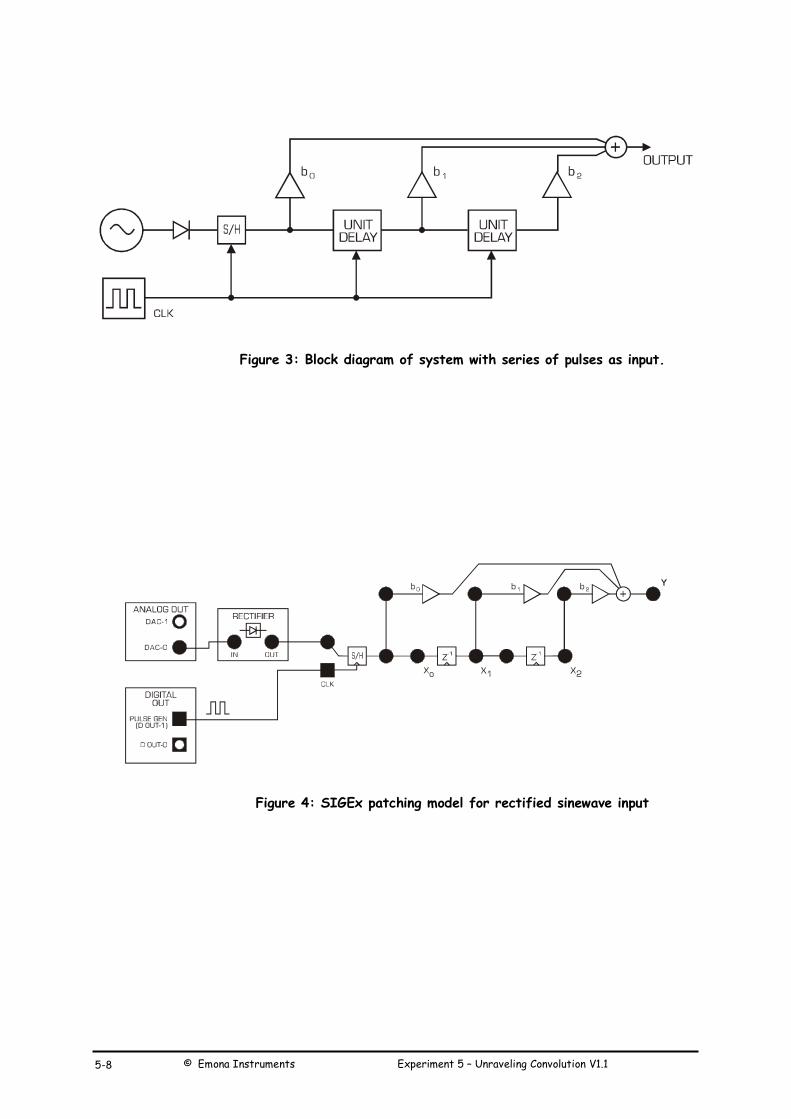
Part 4: rectified sinewave at input
In this exercise the input is a little more interesting than in Part 3: a sequence of three or
four pulses of different amplitude. We obtain the source of this signal from the ANALOG OUT
DAC-0. We then pass this analog signal to the SAMPLE/HOLD block to be sampled and this
becomes our discrete sequence of pulses. Note that the PULSE GENERATOR and DAC signal
generator share the same internal clock and hence no slippage occurs in the scope displays.
Note that although the signal is sampled and becomes “discrete” it has not become a “digital”
signal. This is an important distinction. Rather it now exists as sequential discrete samples of
the original signal. More about sampling and its implications in several later experiments.
Settings are as follows:
PULSE GENERATOR: FREQUENCY=800Hz; DUTY CYCLE: 0.5 (50%)
SCOPE: Timebase 10ms; Rising edge trigger on CH0; Trigger level=1V
Confirm that the sinewave from the DAC-0 is 100Hz, 2V peak, before entering the RECTIFIER.
We will treat the sinewave as a continuous signal and ignore the very small steps present as
these have no consequence to our procedure.
Question 5
Note the amplitude of the half wave rectified sine and explain why its amplitude is reduced
relative to the input ?
© Emona Instruments Experiment 5 – Unraveling Convolution V1.1 5-8
Figure 3: Block diagram of system with series of pulses as input.
Figure 4: SIGEx patching model for rectified sinewave input

Experiment 5 – Unraveling Convolution © Emona Instruments 5-9
15. Maintaining the same values for the b gains as in Part 1 (i.e. b0 = 0.3, b1 = 0.5 and b2 = -
0.2), display the input (i.e., SAMPLE-HOLD output as shown in Figure 5a) and output signals.
Sketch the original half-rectified sinusoid and discrete output from the SAMPLE/HOLD in the
graph below.
Graph 2: inputs and sampled outputs
Confirm that there are 8 samples of each half wave sine input. This is expected as the sampling
clock is 800Hz and the input sinewave is 100 Hz.
Note there are four nonzero pulses in the delay line input sequence and six in the summer
output. The reason for this will emerge as we proceed.
Again, we will carry out a deconstruction of the output signal in terms of the time offset
contributions, i.e. we will trace the output pulse amplitudes in terms of the
input values. We could use the same method as in Part 3, however, there is an
interesting alternative. We will separately observe and compare the three individual
contributions into the output ADDER, i.e. the signals added through gains b0, b1 and
b2 in turn. Examples of these signals are shown in Figure 5b below.

© Emona Instruments Experiment 5 – Unraveling Convolution V1.1 5-10
Figure 5a: example input signal and 4-level sampled signal
Figure 5b: example individual bo, b1 & b2 inputs to adding junction
16. We begin with the contribution through b2. Temporarily disconnect the leads
corresponding to inputs b0 and b1. Observe and record the input and output signals in the graph
above. Confirm for yourself that this result is as expected. View the sampled input on one scope
channel and the individual output on the other scope channel.
17. Now repeat for the b1 and b0 contributions. Only the outputs need be recorded since
the same input is used. Again, verify that the results are as expected.
When completed, you will have three scaled replicas of the input with time offsets.
18. For each time slot, sum the contributions of the three output records and plot the
result. Verify that this agrees with the output signal produced when the three leads are
reconnected to the adder inputs.
Question 6
How does this process relate to the principle of “superposition” ?
In summary, we have just passed a sequence of discrete values (our sampled input) through a
system with a particular response (a series of unit delays with multiplying taps) to produce an
accumulation ( the adder) of discrete product terms which are then output.
Each one of these individual contributions is the scaled and shifted version of the unit pulse
response of this system. Another way of thinking about this system as as it being a series of
weighting coefficients.
Now we need to think about representing this process mathematically.
An obvious way to start is to write a separate formula for the six nonzero output pulse
amplitudes . Let us name them y(1), y(2), …, y(6).

Experiment 5 – Unraveling Convolution © Emona Instruments 5-11
19. Label them on your sketch above. Pay attention to the orientation you use.
Each consists of a sum of three products, i.e., of a tap gain b0, b1, or b2 and an input pulse
amplitude.
The input sequence has eight elements (as previously observed, four of these are zero). Label
these x(1), x(2), …, x(8) (you should find it convenient to choose x(1) = x(2) = x(7) = x(8) = 0).
20. Label these on your sketch above.
Numeric indexing is useful as an aid in looking for the general pattern.
The next step is to use symbolic indexing so that the set of formulas can be condensed into one.
Here are some of the formulas as they appear with numeric indexing:
y(3) = b0 .x(3) + b1 .x(2) + b2 .x(1)
y(4) = b0 .x(4) + b1 .x(3) + b2 .x(2)
y(5) = b0 .x(5) + b1 .x(4) + b2 .x(3)
y(6) = b0 .x(6) + b1 .x(5) + b2 .x(4)
Question 7
Write down the formula for y(2) and y(1) ? Discuss any unexpected differences .
The general pattern is readily apparent. With symbolic indexing, we can replace these with the
single formula
y(n) = b0 .x(n) + b1 .x(n -1) + b2 .x(n - 2)
where n represents the position in the sequence as a discrete time index.
In Part 2, we found that the unit pulse response h(k) for this system is
h(0) = b0 , h(1) = b1 , h(2) = b2 .
Hence we can express the formula for y(n) as
y(n) = h(0) .x(n) + h(1).x(n - 1) + h(2).x(n - 2)
i.e., y(n) = sum over range of k {h(k).x(n - k)}
This simple formula is known as convolution.

© Emona Instruments Experiment 5 – Unraveling Convolution V1.1 5-12
For the discrete signal case we have implemented it is also known as the convolution sum or the
superposition sum. It can also be expressed in this more compact form:
y(n) =
y(n) = x(n) * h(n) where * represents the “convolution” operator.
It provides a neat way of packaging the procedures you carried out in your investigation, and it
allows the range of k to be extended to any desired value. It is the mathematical representation
of the interaction between the input sequence and the unit pulse response of the system.
Note in particular the term x(n-k). Since we are computing in terms of k, this is a time reversed
version of x(k). This issue is put into context further in a later experiment introducing
correlation, an operation which has a similar looking equation. This subject is covered in detail in
the text by Oppenheimer p90 (see Reference section for details)
Question 8
Explain why this term is reversed and what does this mean ?
For the continuous signal case, the summation is achieved using integration and is known as the
convolution integral or the superposition integral. This topic is covered in detail in many texts
including Lathi and Oppenheimer. (see Reference section for details)
In brief, the convolution integral for continuous signals comes about by increasing the number
of discrete samples whilst reducing their width to a limit of 0, such that the sum of many
products can be represented by the integration of the product.
Its equation is
y(t) =
In the above exercise, we obtained the result by means of a superposition of dissected parts of
the unit pulse response. In Part 3 we also used superposition; however, it did not involve
breaking up the unit pulse response. This method was easier to apply for that case because the
input sequence had only two pulses.
Compare the two methods when used with the input in Part 4 (do this with the help of sketch
graphs as before). Consider possible advantages of one over the other as a vehicle for deriving
the convolution formula.
21. Repeat this process with a new system response. Let each tap be equal to 0.333 ie:
b0=b1=b2=0.333.

Experiment 5 – Unraveling Convolution © Emona Instruments 5-13
Question 9
What is a common label for this response ?
Part 5: sinewave input
Up to this point we have used relatively short input sequences. This made it easy to trace the
passage of the pulses through the system since output segments remained distinct and could be
readily referenced to the corresponding input segment. However, we need to consider whether
the formula that we obtained on this basis is also valid in the more general and usual situation
when the input signal is an ongoing stream without breaks.
For this purpose we will go over the steps in Part 4 using a sinewave as input. This means there
is no "natural" reference marker, hence you will need to designate one.
Nevertheless, keeping track of time points will be straightforward since the signal is periodic
and the number of samples per period is relatively small.
22. We use the setup in Part 4, and re-use “full sinewave” output at DAC-0 by bypassing the
RECTIFIER.
As before, since the sinewave frequency is a submultiple of the PULSE GENERATOR clock, no
slippage occurs in the scope displays.
23. Proceed as in Part 4, connecting only one of the three adder inputs. As in Part 4, observe
and record each of the separate output sequences for each input in turn.
As you would expect, these are scaled and delayed replicas of the input, i.e. they are sampled
sinewaves. Carry out spot checks to verify that amplitude and phase relative to the input are
correct. (Reminder, since there are eight samples per period, the phase shift corresponding to
a unit delay is 45 degrees.)

© Emona Instruments Experiment 5 – Unraveling Convolution V1.1 5-14
24. For each time slot, add up the contributions of the three output records obtained above
and plot the result. Verify that this agrees with the output signal produced when all the input
leads are reconnected to the adder.
Graph 3: sinewave input signals
Now we are ready to revisit the formula obtained in Part 4. Proceed as before and show that
the formula remains valid for this case.
Question 10
Show that the formula remains valid.
This completes the basics of the convolution formula.

Experiment 5 – Unraveling Convolution © Emona Instruments 5-15
In the next task we take a closer look at the output signal obtained in Part 5, and show that it is
a sampled sinewave. This is a discrete-time example of the investigation in Lab 4, where we
discovered that when the input of a linear system is sinusoidal, the output will also be sinusoidal.
25. Confirm that the eight pulses making up one period of the output sequence represent
samples of a sinewave. A straightforward method is to exploit the sum of squares identity.
Since there are eight samples per period, you can match pairs of samples that are 90 degrees
apart (how many pairs can you find?). Note that knowledge of the peak amplitude is not essential
for this (all that is needed is to show that the sum of the squares is the same for each pair).
Question 11
Show your working for the sum of squares analysis ?
26. Use the FUNCTION GENERATOR tuned to 100 Hz to provide the alternative
unsynchronized sinewave input. Set it to an amplitude of 2Vpeak (4V pp). The resulting slippage
effectively produces an interpolation of the samples -- a useful exploitation of something that
is usually unwanted!
Now that we have a simple way of displaying the input and output sinewaves, an interesting
additional item to examine is the theoretical verification of the measured output/input
amplitude ratio and phase shift. The peak values are clearly apparent, so the amplitude ratio
measurement is straightforward. Similarly, the now discernible zero crossings can be used for
the phase shift measurement.
The math for the theoretical verification is done by means of the application of the formula for
reducing the sum of sinusoids .
In the next Part we investigate an example of effects that can be obtained by means of suitably
chosen values for the tap gains.

© Emona Instruments Experiment 5 – Unraveling Convolution V1.1 5-16
Part 6: mystery application
Here we explore a special application of convolution. The setup is the same as for Part 5,
except for new tap gains in the delay line. Two sets will be tested.
The first is b0 = 0.3 , b1 = 0.424 , b2 = 0.3
The second set is b0 = -0.3 , b1 = 0.424 , b2 = -0.3
27. When the tap gains have been adjusted to the first set of values,( b0 = 0.3 , b1 = 0.424 ,
b2 = 0.3), display the output, and measure the amplitude and phase relative to the input as in
Part 5. Confirm that this is in agreement with theory.
28. Alter the tap values to the second set of values (b0 = -0.3 , b1 = 0.424 , b2 = -0.3) and
repeat the measurements. Is the outcome predicted by theory ?
29. Vary the frequency of the sinewave over a suitable range to demonstrate that sinewave
inputs with frequencies near 100 Hz are heavily attenuated.
Question 12
Why is the outcome obtained above described as filtering?
In other labs you will discover how to choose the tap gains to design different kinds of
responses versus frequency.

Experiment 5 – Unraveling Convolution © Emona Instruments 5-17
Tutorial questions
Q1 Look up your textbook to find out the name given to systems that have the structure in Figure 1, i.e. without feedback. Consider an alternative discrete-time system that has a single delay element with feedback (refer to your textbook if needed). Show how to apply the convolution formula in this case.
Q2 Consider the condition(s) required to avoid infinite output values in applications where the unit pulse response is not time limited. Show to avoid an unstable output in the feedback system in Q1.
Q3 Consider a process that consists of taking a running average of a data sequence, such as atmospheric pressure. Suppose we do this by taking the sum of 50% of the middle value, and 25% of the preceding and following values. Can this process be described as convolution? If so, write down the unit pulse response.
Q4 Using integration instead of discrete summation, write down a continuous-time version of the convolution formula in terms of the system impulse response.

© Emona Instruments Experiment 5 – Unraveling Convolution V1.1 5-18


© Emona Instruments Experiment 8 – A Fourier Series analyser V1.1 8-2
Experiment 8 – A Fourier Series analyser
Achievements in this experiment Compose arbitrary periodic signals from a series of sine and cosine waves. Confirm the Fourier Series equation. Compute fourier coefficients of a waveform. Build and use a Fourier Series analyser. Demonstrate that periodic waveforms can be decomposed as sums of sinusoids. Introduce complex notation.
Preliminary discussion In Lab 3 we discovered that sinewaves are special in the context of linear systems (time invariance assumed). Unlike other waveforms, a sinewave input emerges at the output as a sinewave. We saw in Lab 4 that this makes it possible to completely characterize the behaviour of a system in this class by simply measuring the output/input amplitude ratio and the phase shift of the sinewave as a function of frequency. Now, this is fine if we only need to process sinewaves -- is it feasible to make use of this when dealing with other kinds of inputs ? For example, when the input is a waveform like the sequence of digital symbols we investigated in Lab 4. One possibility is to see whether a nonsinusoidal waveform could be expressed as a sum of sinewaves, over a suitable frequency range, either exactly, or even approximately. If this could be done, the system output can then be obtained by exploiting the additivity property of linear
systems, i.e., first obtain the output corresponding to each sinusoidal component of the input signal, then take the sum of the outputs. This was covered in Lab 4. In this Lab we explore this idea by means of an ancient technique based on the generation of beat frequencies -- somewhat like when a musician uses a tuning fork. We will begin by adding together many beat frequencies and view the resulting waveform. From there we will look at the equations and use what we know from trigonometry to decompose waveforms into their constituent components. Pre-requisites:
Familiarization with the SIGEx conventions and general module usage. A brief review of the trigonometry required will be covered as needed.

Experiment 8 – A Fourier Series analyser © Emona Instruments 8-3
Equipment
� PC with LabVIEW 2009 (or higher) & “Digital Filter Design” toolkit installed
� NI ELVIS 1, 2 or 2+ and USB cable to suit
� EMONA SIGEx Signal & Systems add-on board
� Assorted patch leads
� Two BNC – 2mm leads
Procedure
Part A – Setting up the NI ELVIS/SIGEx bundle
1. Turn off the NI ELVIS unit and its Prototyping Board switch. 2. Plug the SIGEx board into the NI ELVIS unit. Note: This may already have been done for you. 3. Connect the NI ELVIS to the PC using the USB cable. 4. Turn on the PC (if not on already) and wait for it to fully boot up (so that it’s ready to connect to external USB devices).
5. Turn on the NI ELVIS unit but not the Prototyping Board switch yet. You should observe the USB light turn on (top right corner of ELVIS unit).The PC may make a sound to indicate that the ELVIS unit has been detected if the speakers are activated. 6. Turn on the NI ELVIS Prototyping Board switch to power the SIGEx board. Check that all three power LEDs are on. If not call the instructor for assistance. 7. Launch the SIGEx Main VI. 8. When you’re asked to select a device number, enter the number that corresponds with the NI ELVIS that you’re using. 9. You’re now ready to work with the NI ELVIS/SIGEx bundle. 10. Select the Lab 8 tab on the SIGEx SFP.
Note: To stop the SIGEx VI when you’ve finished the experiment, it’s preferable to use the STOP button on the SIGEx SFP itself rather than the LabVIEW window STOP button at the top of the window. This will allow the program to conduct an orderly shutdown and close the various DAQmx channels it has opened.

© Emona Instruments Experiment 8 – A Fourier Series analyser V1.1 8-4
The experiment
Part 1 – Constructing waveforms from sine & cosines
A simple sinusoid with zero phase can be represented by the equation (Eqn 1) And a cosinewave with a frequency of n times can be simply represented by the equation (Eqn 2) Any wave which is an integer multiple of another frequency is known as a harmonic of the frequency. So equation 2 represents the harmonics of the signal in equation for n >1. We can use the “harmonic summer” simulation in Experiment TAB 8 to view and sum multiple signals which are harmonics of the fundamental signal ie: the signal for n=1. Harmonics for which n is even are known as even harmonics, and when N is odd are called odd harmonics. This simulation allows us to view and sum any sinusoid for which 1 <= n <= 10, that is, the fundamental and nine harmonics. The numeric entry boxes allow you to enter the amplitude of each sinusoid.
11. Experiment a little by entering various amplitudes into the numeric entry boxes for the cosine row. Confirm for yourself visually that what is displayed is as you would expect. 12. Set all amplitudes to zero, except for the “1st” component, the fundamental, which you can set to 1. Moving from the second to the ninth sequentially, set each amplitude to the equal to 1. As you do this notice how the combined signal is changing. Do this for the cosine row ONLY at this point. Question 1
How would you expect the summation of to look if you could add up many more harmonics ?
Question 2
What is its peak amplitude and is this as expected ?
Question 3
Is the fundamental an odd or even function ? Is the summation odd or even ?

Experiment 8 – A Fourier Series analyser © Emona Instruments 8-5
Question 4
Write the equation for the summation of the 10 signals ? Is it symmetrical about the X axis?
Question 5
Vary the amplitudes and notice how the signal changes . You may set the amplitude of certain components to 0 as you see fit. Can you create a wave form which starts at a zero value ? Write the equation for your new varied amplitude signal ? Does it start at a zero value ?
13. Sketch your arbitrary wave form, for which you have just written the equation, below.
Graph 1: sine wave summation

© Emona Instruments Experiment 8 – A Fourier Series analyser V1.1 8-6
The general form of the equation for the summation of cosine harmonics is as follows:
where are the amplitude values of each cosine wave. 14. Set all cosinewave amplitudes equal to 0 and now set the sine waveform amplitudes equal to 1, starting from the first harmonic and moving sequentially until the 10th harmonic. Notice how the summation changes as you add harmonics. Question 6
How would you expect the sine summation of to look if you could add up many more harmonics ?
Question 7
What is its peak amplitude and is this as expected ? Is this an odd or even function ?
Question 8
Vary the amplitudes and notice how the signal changes . You may set the amplitude of certain components to 0 as you see fit. Can you create a wave form which starts at a non-zero value ? Write the equation for your new varied-amplitude signal ? Does it start at a non-zero value ? Is it symmetrical about X axis.?
The general form of the equation for the summation of sine wave harmonics is as follows:
where are the amplitude values of each sine wave.
The general form for the summation of both sine and cosine harmonics is:

Experiment 8 – A Fourier Series analyser © Emona Instruments 8-7
Even functions are symmetrical about the Y axis. Odd functions are not symmetrical about the Y axis, but appear to be inverted about the X axis on the negative side of the Y axis. Sine and cosine waves, as well as their sums of sine and cosines, are always symmetrical about the X axis. Being symmetrical means that they cannot represent a DC offset. In order to have a
DC offset we must add a constant to the equation. 15. Add a DC component to the signal by inputting the value into the DC numeric entry box ? Let us add a value a0 to represent that constant and the general equation for our arbitrary wave form becomes
where N is max number of harmonics present. In our experiment above, N=10. This equation describes any arbitrary wave form with the proviso that it is periodic. Any periodic waveform, no matter how complicated, can be represented by the summation of many simple sine and cosine waveforms. This equation is known as the Fourier series equation, naturally enough named after Jean Baptiste Joseph, Baron de Fourier, 1768 – 1830.
Figure 1: Portrait of Joseph Fourier
Let us have a further look at this important equation. When N equals one, this frequency known as the fundamental frequency, is also called the resolution frequency. Being the smallest frequency in this series it defines the minimum
separation between components in a particular waveform. In the Fourier series equation above we have grouped waves in terms of whether they are sine or cosine waveforms. Let us now modify this equation and group individual components by their harmonic number. This is easy enough and is as follows

© Emona Instruments Experiment 8 – A Fourier Series analyser V1.1 8-8
Grouping in this way allows us to think of each frequency as having both a sine and cosine component. Let us have a quick revision of what adding a sine and a cosine of the same frequency together may result in. 16. Using the “harmonics summer” simulation in the Experiment 8 TAB of the SIGEx SFP, set all amplitudes including that of the DC equal to 0. Set the amplitude of the sine and cosine first harmonic equal to 1. View the resulting summation. Question 9
Write the equation for the summation of these 2 waves ? Write the equation for the summation in terms of the sine wave with a non zero phase shift.
17. Vary the amplitudes from 0 to 1 and notice how the signal changes . Question 10
Describe how the summation changes as you vary the respective amplitudes?
Question 11
For a particular pair of amplitudes you have set, write the equation for the summation in terms of sine and cosine as well as its equivalent polar representation ?

Experiment 8 – A Fourier Series analyser © Emona Instruments 8-9
18. Sketch a vector or for phasor representation of these two signals and their resulting summation, known as the resultant.
Graph 2: components & resultant
For each harmonic, nwt, a signal may have a sine and cosine component, implemented by their own respective amplitude, an and bn. It is helpful to think about these component pairs as a single entity at a particular frequency. The only difference between them being their respective amplitude and the respective orientation or phasing. We know that a sine wave is 90° out of phase with a cosine wave, a quality which makes those two components orthogonal to each other. By orthogonal we mean that they operate independently of each other. And so we need a notation and document these two-dimensional pair of components and this notation is provided to us by Euler with his famous equation:
Where j the notes the component at 90° out of phase with the other component, hence the sine and cosine pair.

© Emona Instruments Experiment 8 – A Fourier Series analyser V1.1 8-10
Hence we can replace all sine/cosine pairs at a particular harmonic n with the complex exponential function ejnwt, and in this way the Fourier series can be rewritten as
where Cn represents the resultant from the pair of respective amplitudes for the sine and cosine components. ie: Cn
2 = bn2 + an
2, and is known as the “complex fourier series”. Euler's formula allows us to process the sine/cosine component pair , simultaneously, rather than individually. It is a form of two-dimensional notation where the sine and cosine components for a frequency are instead treated together as a resultant with particular phase ie polar notation. This notation is known as “complex” notation and was introduced in the previous experiment, Experiment 7.
Remember that the practical part of this experiment just completed above shows us how a resultant waveform is represented by two orthogonal components. Part 2 – Computing Fourier coefficients
In the previous part of this experiment we discovered that we can construct any arbitrary periodic waveform by the summation of a number of sine and cosine harmonics. This knowledge is the basis of signal synthesis and in this part of the experiment we will do the reverse process, that is, the analysis of an arbitrary wave form to discover the presence and amplitude of its constituent harmonics. We call these amplitudes the Fourier coefficients of the waveform as they are the coefficients within the Fourier series equation we have just derived. Armed with only some basic trigonometry we will now explore some more qualities of sinusoids. Before we create our arbitrary wave form to be analysed let us determine some rules with
which we can build our analyser. We know that the area under a sine wave or a cosine wave over a timeframe of one period will always be equal to 0. Consequently we know that the area under a sine wave or cosine wave for a timeframe of any number of periods will also be equal to 0. To determine the area mathematically we would integrate over the timeframe of interest. This process would give us the average value of the signal during that time. This average value is the DC component of the signal.
Figure 2: model for integrating one period of a sinusoid

Experiment 8 – A Fourier Series analyser © Emona Instruments 8-11
The INTEGRATE & DUMP module can be used to integrate over a single period as denoted by the input clock. This is well suited to integrating periodic waveforms such as sinusoids and products thereof. In this next exercise we will integrate a sinusoid over a single period to prove the assertion that the area under a sine wave or a cosine wave over a timeframe of one period will always be equal to 0.
19. Connect the model as per Figure above. The clock connection is necessary for this module, unlike for the continuous time INTEGRATORS on the SIGEx board. Settings are as follow: SCOPE: Timebase: 4ms; Trigger on Ch0; Connect Ch0 to CLK input; Level=1V FUNCTION GENERATOR: Select SINE output, AMPLITUDE = 4vpp, FREQUENCY=1kHz Refer to the SIGEx User Manual for instructions on how the I&D and I&H functions work if this is not obvious. NOTE: The I & D period is from positive clock edge to positive clock edge. Question 12
What is the output value at the end of the integration period ? HINT: the I&H function will hold the final value.
20. While viewing the I&D output, to broaden your understanding of the integration process, change the incoming signal from sine to triangle to bipolar squarewave at the FUNCTION GENERATOR VI and confirm that the integrated output is as you would expect over one period. You should be able to confirm that integration is the accumulation of the total signal charge, with positive signals adding to the total, and negative signals subtracting from the total. Another way of extracting the DC component of a signal is by using a filter which is tuned to a sufficiently low-frequency to exclude all harmonics except for the DC component. The integration process you have just explored is also a form of filtering, (as discussed in Experiment 6 on matched filtering.) We will use the filtering method next. Note that in this next part of the experiment the signals we are using are generated from data arrays in LabVIEW and output in a synchronized manner from the ANALOG OUT terminals
DAC-0 and DAC-1.These signals are thus synchronized to each other, just as they appear on screen and in the textbook. 21. Using the left hand side of Experiment 8 TAB of the SIGEx SFP, select a sine wave , 1st harmonic. Connect DAC-1 to the input of the TUNEABLE LPF and view both input and output with the scope. Settings are as follow: SCOPE: Timebase 20ms; Rising edge trigger on CH0; Trigger level=0V TUNEABLE LPF: GAIN=mid position Adjust the frequency control, fc, of the TLPF from fully clockwise counterclockwise until the output signal is a DC value.
© Emona Instruments Experiment 8 – A Fourier Series analyser V1.1 8-12
Confirm that this DC value is approximately 0 V. Try this test for several harmonics. Change the “sine harmonic” value to 2,3 or 5 etc to try this. INSIGHT 1: average value of an integral number of periods of sine or cosine waves equals zero. Note that as far as the filter is concerned a single cosine wave is the same as a sine wave, so Insight 1 holds true for both. You can vary the phase of the sinewave out of DAC-1 using the “sine phase” control. The signal out of DAC-0 remains constant as a cosine wave.
22. Set the “sine harmonic “ value back to 1. Set “sine phase” to 0. View DAC-1 with CH1 and DAC-0 with CH0. Settings as follows: SCOPE: Timebase 20ms; Rising edge trigger on CH0; Trigger level=0V DAC-1 will be a sine wave and DAC-0 a cosine wave, relative to each other. Connect as shown in the figure below. View the output of the MULTIPLIER as well as the output of the TUNEABLE LOW PASS FILTER.
Figure 3: comparing sinusoids You will now multiply a sine wave by a cosine wave and determine its average value. Repeat this with the second and third harmonic of the sinusoid. Question 13
What is the average value of these three products ?
INSIGHT 2: average value of an integral number of products of any sine or cosine harmonics equals zero. 23. Set the “sine harmonic “ value back to 1. Set “sine phase” to 90. View DAC-1 with CH1 and DAC-0 with CH0. Settings as follows: SCOPE: Timebase 20ms; Rising edge trigger on CH0; Trigger level=1V

Experiment 8 – A Fourier Series analyser © Emona Instruments 8-13
DAC-1 will now be a cosine wave and so will be DAC-0. NB: This is relative to the start of the signal data array. See the ANALOG OUT VIEWER window for confirmation. Connect as shown in the figure above. View the output of the MULTIPLIER as well as the output of the TUNEABLE LOW PASS FILTER with the scope. You will now multiply a cosine wave by itself and determine its average value. Repeat this with the second and third harmonic of the cosine wave.
Question 14
What is the average value of these products ?
INSIGHT 3: average value of an integral number of products of any sine by its harmonic equals zero. INSIGHT 4: average value of an integral number of products of any sine by itself equals a non zero value.The same holds for cosine.
Question 15
Write the complete formula for the product of a cosine, Acoswt, by itself? What do the terms represent?
At this point we can see that the only product to yield a non-zero average value is that of a sine wave by the same sine wave. The same is true for cosine. So if we multiply an arbitrary waveform by a particular “probing” sine or cosine harmonic and extract the average value of this product there will only be non-zero when that arbitrary wave form contains that particular “probing” harmonic as one of its constituent components. This is a very powerful insight and allows us to have a simple tool with which to analyse arbitrary wave forms. Let us now give this a try.
24. Construct the following arbitrary wave form using the HARMONIC SUMMER on the right hand side of the SIGEx SFP, Experiment 8 TAB. Settings are as follows : Cosine amplitudes: 1, 0, 0.5,0,0,1,0,0,0,0 Sine amplitudes: 0,0.3,1,0,0,0,2,0,0,0 DC level: 0.5 Switch “to DAC-0” ON: This will output the summation to DAC-0. See the ANALOG VIEWER window. Set “sine harmonic” =1; Set “sine phase = 0. This signal is output to DAC-1. SCOPE: Timebase 20ms; Rising edge trigger on CH0; Trigger level=0V

© Emona Instruments Experiment 8 – A Fourier Series analyser V1.1 8-14
Figure 4: comparing sinusoids 25. You will need to now ensure that the overall gain of the MULTIPLIER and TLPF is unity. We know from the User Manual specifications that the MULTIPLIER gain is approximately unity, whereas the TLPF GAIN is variable. Connect both MULTIPLIER inputs to the same 1st
harmonic sinewave and view the output. The input from the DAC is 4Vpp whereas the output is approx. 4.4Vpp…slightly greater than unity gain. While viewing the TLPF output, turn the fc control clockwise to pass the entire signal. Adjust the TLPF gain precisely for a 4Vpp output. 26. Return to your previous setup but do not touch the TLPF GAIN setting for the rest of the experiment. At this point we are multiplying the arbitrary wave form which investigated by a first harmonic sine wave.
Figure 5: screenshot of SIGEx SFP Tab “Lab 8” including
harmonic generator bottom left, and summer on the right
27. View the product at the output of the multiplier on CH0 and the TLPF output. Adjust the TLPF frequency control to isolate the DC component. Note the value of the DC level as the amplitude of the first harmonic sinusoid in the table below. Increase harmonics one by one, adjust theTLPF frequency setting if necessary and note the amplitude for the remaining 10 harmonics in table.

Experiment 8 – A Fourier Series analyser © Emona Instruments 8-15
Now to analyze for the cosine components. 28. Set “sine harmonic” back to 1. Change “sine phase” to 90. This will convert the sine wave into a cosine wave , as sin(wt + 90) = cos(wt). Repeat the above steps to all 10 cosines and enter your measurements of the TLPF DC output level into the table . Once complete, set the phase back to 0 degrees and complete the measurements for all sine harmonics into the table.
Table of measured coefficients
29. Connect the input of the TLPF directly to the arbitrary wave form at DAC-0 to measure the DC value of that waveform alone, and enter into the table at “DC (V) = “. Question 16
How do your readings compare with expectations ? . Explain any discrepancies .
30. While you have the experiment setup, vary the harmonic summer settings and see the resulting output from the TLPF. Experiment a little with values while you get the chance.
Harmonic
number
sine
(V)
cosine
(V)
1st
2nd
3rd
4th
5th
6th
7th
8th
9th
10th
DC (V) =

© Emona Instruments Experiment 8 – A Fourier Series analyser V1.1 8-16
Part 3 – Build a manually swept spectrum analyzer In the previous part of this experiment we use synchronised signals which were generated in LabVIEW and output via the DACs of the ANALOG OUT module. In this part of the experiment we will analyse the constructed arbitrary signal using an independent sinusoid generator, that is, the FUNCTION GENERATOR.
Figure 6:building a “wave analyzer”
31. Once again construct the following arbitrary waveform using the HARMONIC SUMMER
of the SFP, Experiment 5 TAB. Launch the FUNCTION GENERATOR as well. Settings are as follows : Cosine amplitudes: 1, 0, 0.5,0,0,1,0,0,0,0 Sine amplitudes: 0,0.3,1,0,0,0,2,0,0,0 DC level: 0.5 Switch “to DAC-0” ON SCOPE: Timebase 20ms; Rising edge trigger on CH0; Trigger level=0V FUNCTION GENERATOR: Frequency=100Hz, Amplitude=4Vpp, Sine wave selected 32. Move the input to the multiplier which was connected to DAC-1 to the FUNC OUT terminal of the FUNCTION GENERATOR . This signal will be a 4Vpp sine wave at 100 Hz. View both inputs to the multiplier on the scope. One is the arbitrary waveform, the other is the 100 Hz sine wave. Question 17
What do you notice about their phase relationship ? Is this to be expected ? Explain.
If the inputs are drifting relative to each other then you would expect the product of the inputs to also be slowly varying. 33. View the sinusoid and the product, output of the multiplier, at the same time and confirm that it is slowly varying. As it varies it will pass through the point of interest, the interface point that we wish to measure. This point occurs twice per cycle lasts creating both are maxima and minima. If we detect either the maximum of the minima the absolute value of these will give us the average
DC value which we require.

Experiment 8 – A Fourier Series analyser © Emona Instruments 8-17
You may wish to review your understanding of why these maximas and minimas occur when signals drift relative to each other. You can use both trigonometry and/or the DAC outputs and the MULTIPLIER module to revisit this topic. 34. Now view both the output from the FUNCTION GENERATOR and the output of the TLPF. Adjust the frequency of the TLPF to isolate only the DC component and confirm that it has a maxima and a minima. HINT: if the DC value is varying too slowly, or you are impatient, or just inquisitive (…a good thing), increase the frequency at the function generator by 1 Hz. This
will make your DC value vary at a rate of approximately 1 Hz. Trigger on the sinewave from the FUNCTION GENERATOR for a stable display. 35. Vary the frequency of the function generator in steps of 100 Hz starting from 100 Hz up to 700 Hz. Note the maximum value of the DC output in the table below. It will be more accurate to measure peak to peak and then halve it.These will be the measured amplitudes of the constituent harmonics making out the arbitrary wave form. How do they compare with the actual amplitude value entered into the SFP itself.?
Table of measured coefficients
Question 18
Can you explain if your readings differ in some places from the actual value ? HINT: you have one value per harmonic instead of two. Consider the previous discussion above about resultants in your answer. And to allow for MULTIPLIER and TLPF gains.
Whilst the theoretical modeling with the synchronized sine and cosine waves from the previous part is able to yield the constituent sine and cosine components, a real world signal without the
Input
frequency (Hz)
TLPF output
pp swing (V)
Half of
pp (V)
Entered
values
Calculated
resultant (V)
100
200
300
400
500
600
700
DC (V) =

© Emona Instruments Experiment 8 – A Fourier Series analyser V1.1 8-18
benefit of synchronization can only measure the resultant amplitude. This is shown in the exercise just completed. 36. This section of the experiment was about building a manually swept spectrum analyser. The function generator instrument has the ability to be automatically swept. As an exercise in automation enter an appropriate start, stop frequency, say 101 & 1001 Hz, as well as step size of 100 Hz and a step interval of 2 seconds and allow the function generator itself to sweep the analysing frequency while you view the amplitude of the DC value from the analyser which
corresponds to the amplitude of each harmonic present. Display the FUNCTION GENERATOR sinewave also, and trigger the scope on it for a stable display of 4Vpp. Set the AUTOSCALE to OFF. Congratulations, you have just constructed a swept spectrum analyzer using basic mathematical blocks. Part 4 – analyzing a square wave
We will now use our manually swept spectrum analyser to investigate which harmonics at present in a square wave. The experiment set up is as for the previous section except that now the input is taken from the PULSE GENERATOR module output.
Figure 7: working with a square wave
37. Vary the patching as shown in figure 7 above . Settings are as follows: FUNCTION GENERATOR: Frequency=100Hz, Amplitude=2Vpp, Sine wave selected
PULSE GENERATOR: FREQUENCY=100Hz, DUTY CYCLE=0.5 (50%) SCOPE: Timebase 20ms; Rising edge trigger on CH1; Trigger level=0V 38. Vary the frequency of the function generator in steps of 100 Hz starting from 100 Hz up to 700 Hz. (Remember, you can vary the input frequency by 2 Hz to speed up the resultant DC oscillation display).Note also the maximum value of the DC output in the table below. These will be the amplitudes of the constituent harmonics making up the squarewave. You may know from theory that a square wave of 50% duty cycle contains only odd harmonics. This can help you focus your investigation around the appropriate frequencies.

Experiment 8 – A Fourier Series analyser © Emona Instruments 8-19
Table of measured coefficients for squarewave
Question 19
Why are some of the harmonics hard to detect ?
Varying the duty cycle of the PULSE GENERATOR from the SFP control “DUTY CYCLE”, for example to 0.2 (20%) will introduce even harmonics. Question 20
Can you now detect even harmonics in the squarewave of 20% duty cycle ?
View the output from the MULTIPLIER to see what signal you are measuring and extracting the DC value from. Comparing measured Fourier series coefficients to theory
From the theory the relative value of the Fourier series coefficients for a 50:50 square wave is a series like so: 1, 1/3, 1/5, 1/7….1/n where n is the odd harmonic present in the squarewave.
Input
frequency (Hz)
TLPF output
amplitude (V)
Scaled measured values
(V)
Calculated
resultant (V)
100
200
300
400
500
600
700
DC (V) =

© Emona Instruments Experiment 8 – A Fourier Series analyser V1.1 8-20
Question 21
Compare your measured coefficients for the first 4 odd harmonics as ratios to that expected by theory ? Remember to normalize the measurements for the comparison.
References Langton.C.,”Fourier analysis made easy ”, www.complextoreal.com


© Emona Instruments Experiment 11 – Poles & zeros in the Laplace domain V1.1 11-2
Experiment 11 – Poles and zeros in the Laplace domain
Achievements in this experiment You will discover how poles and zeros can be used to visualize frequency responses graphically at a glance, in a minimal-math zone. You will be able to use this knowledge to intuitively design low order continuous-time responses. You will be ready to extend this concept to higher order systems, and discrete-time applications
Preliminary discussion In the early days of linear system design, long before the advent of programmable computing, numerous graphical techniques were invented to get around the arithmetic tedium required to calculate system responses. One of these is the pole-zero technique. A century on, this scheme has remained in the system engineer's tool kit because it provides a medium for the intuitive visualization of system behaviour, especially in regard to stability and sensitivity. And, with some circuit structures, there is a bonus: by observing the movement of the poles and zeros, you can intuitively predict system response variations as components are tuned. Part 1: We examine the behaviour of lowpass and bandpass responses generated with the second order feedback system in Fig. 1 in the context of poles and zeros. Part 2: The findings in Part 1 are extended to create special filters realized with the feedback-feedforward system in Fig. 2. The pole-zero paradigm is applied to discover intuitive interpretations of the associated equations. Part 3: We discover how maximally flat and critically damped responses are generated. It should take you about 60 minutes to complete this experiment, not including the preparation to be done before the hands-on lab work.

Experiment 11 – Poles & zeros in the Laplace domain © Emona Instruments 11-3
Pre-requisite work Preparation will be required in order for the hands-on lab work to make sense. This guided preparation is a revision of theory you will have covered in lectures and is presented below as a number of computation exercises. This work should be completed before attempting the lab. Question 1 For the system in Figure 1, obtain a differential equation relating the output x0(t) and the input u(t). Show by substitution that x0 = e
jωt is a solution and determine the corresponding input u(t) that produces this output.
If you are uncomfortable with a complex-valued function to represent the behaviour of a
system that is supposed to operate with real-valued signals, x0 = cos(ωt) or sin(ωt) could be used. However, you will quickly discover that the exponential function has a very useful property that simplifies the math considerably. Remembering that cos(ωt) is Re{ ejωt}, you can carry out the analysis with ejωt then simply take the real part of the result. Practitioners generally don't bother with the formality of taking the real part. Moreover, complex valued signals are easily realized in digitally implemented systems, and indeed, frequently used, for example in modulators and demodulators of dial-up modems.
INPUT
u
x 1 x 2 x 0
-a 1
-a 0
Figure 1: schematic of 2nd order integrator feedback structure without feedforward. Question 2 From the above, with x0 = e
jωt, obtain an expression for the ratio x0/u as a function of jω (not just "ω"; the reason for this will emerge shortly). Note that this ratio is complex valued. Then, obtain its magnitude and phase shift as functions of ω (not jω).

© Emona Instruments Experiment 11 – Poles & zeros in the Laplace domain V1.1 11-4
Question 3
From the results in Question 1 above, plot the magnitude |x0/u| versus ω (radians/sec) for the case a0 = 0.81, a1 = 0.64 . Note that there is a progressive fall off as ω increases. Hence, we can think of this system as realizing a lowpass filter.
Graph 1:response plot Question 4 We now consider an alternative way of getting the response. With a little algebra we create a graphical medium that will provide an intuitive environment for visualizing and generating both magnitude and phase responses.
First, return to the expression for x0/u obtained in (a) and replace "jω" by the symbol "s". Look upon s merely as a convenient stand in for jω. It is not necessary to ascribe any deeper significance to this substitution for the purposes of this lab. The result is the (complex-valued) rational function
x0/u = H(s) = 1/(s2 + a1.s + a0) (Eqn 1).
For the case a0 = 0.81, a1 = 0.64 (as in (b), express the denominator quadratic in the factored
form (s - p1)(s - p2), where p1 and p2 are the roots. Show that these are given by
p1 = 0.9(cos(110.8°) + j.sin(110.8°)) = 0.9expj0.616π
p2 = 0.9(cos(110.8°) - j.sin(110.8°)) = 0.9exp-j0.616π (Eqn 2).

Experiment 11 – Poles & zeros in the Laplace domain © Emona Instruments 11-5
Question 5 Express the complex points p1 and p2 from equation 2 above as the non-exponential complex form of a + ib, that is, with a real and imaginary part.
Question 6
Next, we look at a graphical approach for evaluating the factors (s - p1) and (s - p2). Place
crosses ("x") on a complex plane at the locations corresponding to p1 and p2, as obtained in (c)
above. Place a dot at the point 1.2 on the j axis, i.e., the complex value jω = j1.2 . Join this point and the crosses at p1 and p2 with straight lines. Satisfy yourself that the lengths of these
joining lines are |jω - p1| and |jω - p2|. Noting that 1/|H(jω)| is the product of these two magnitudes, estimate |H(j1.2)|.
Graph 2: vector subtraction

© Emona Instruments Experiment 11 – Poles & zeros in the Laplace domain V1.1 11-6
Question 7 Use the idea above to obtain estimates of |H| at other frequencies and thus produce a sketch graph of |H| over the range 0 to 5 radian/s. (ie: ω will range from 0 to 5). Notice that the presence of a peak in the response is obvious from the behaviour of the vector from p1 as the dot on the j axis is moved near p1. Note that this vector has much greater influence than the other vector, especially near the peak. Compare this estimate with the computed result you obtained in (b). Plot at least 4 points over this range, choosing your points to reflect the important characteristics of this response. Explain why the vector from p1 has a greater influence on the peak of the response.
Graph 3:plot the calculated magnitude response |H(jw)|
Question 8
The roots p1 and p2 of the denominator polynomial of H(s), marked as crosses on a plane of the
complex variable s are known as poles of H(s). Note that in the example case, p2 is the complex
conjugate of p1. Why is this so?
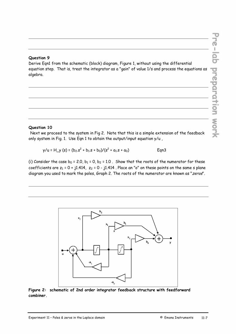
Experiment 11 – Poles & zeros in the Laplace domain © Emona Instruments 11-7
Question 9 Derive Eqn1 from the schematic (block) diagram, Figure 1, without using the differential equation step. That is, treat the integrator as a "gain" of value 1/s and process the equations as algebra.
Question 10 Next we proceed to the system in Fig 2. Note that this is a simple extension of the feedback only system in Fig. 1. Use Eqn 1 to obtain the output/input equation y/u ,
y/u = H_y (s) = (b2.s2 + b1.s + b0)/(s
2 + a1.s + a0) Eqn3
(i) Consider the case b0 = 2.0, b1 = 0, b2 = 1.0 . Show that the roots of the numerator for these
coefficients are z1 = 0 + j1.414, z2 = 0 - j1.414 . Place an "o" on these points on the same s plane
diagram you used to mark the poles, Graph 2. The roots of the numerator are known as "zeros".
x
2
x
1
x
0
-a
1
-a
0
b
b 0
b 1
2
b 2
y
u
Figure 2: schematic of 2nd order integrator feedback structure with feedforward combiner.

© Emona Instruments Experiment 11 – Poles & zeros in the Laplace domain V1.1 11-8
Question 11 Using the zeros with the method from Question 6, carry out the graphical estimation of the numerator of Eqn 3 at s = j1.2. Note that this is a special case, with the zeros located on the j
axis (since b1 = 0). Hence, the lines joining the point jw and the zeros will lie on the j axis.
Combine the numerator and denominator estimates to obtain |H_y(j2)|. Extend to other values of w, and sketch the magnitude response |H_y(jω)|. Comment on the presence of a null at ω = 1.414.
Question 12 (optional) Compute |H_y(jω)| from Eqn 3 and assess the quality of the estimate based on poles and zeros.
Question 13
With a0 and a1 as in Question 3, apply the pole-zero method to obtain approximate graphs of the magnitude response for the following cases:
b1 = 1, b0 = b2 = 0
b2 = 1, b0 = b1 = 0
b2 = 1, b1 = −a1, b0 = a0 b2 = 1, b1 = 0, b0 = a0 State the name of the response type corresponding to each case (e.g., bandstop, allpass, etc).
For the allpass case, plot the phase and/or group delay response (group delay = − d(phase)/dω). Find out and note here an application for the allpass response.

Experiment 11 – Poles & zeros in the Laplace domain © Emona Instruments 11-9
Graph 4: various responses
Question 14 The integrators in Figs 1 and 2 were depicted as having unity gain. A practical realization normally has an associated gain constant. The corresponding integrator equations have the form
x0 = k . ∫(x1) dt
x1 = k . ∫(x2) dt Note that k is not dimensionless. Its unit is sec-1. The SIGEx INTEGRATOR modules provide a choice of four values of k, selectable by means of on-board switches. The switches are labelled “INTEGRATION RATE” and the selection and associated value is displayed on the SIGEx SFP. Suppose k = 12,500 sec-1 is selected. Modify the frequency scale for the response in (b) above to reflect this choice of k. Explain your reasoning here.

© Emona Instruments Experiment 11 – Poles & zeros in the Laplace domain V1.1 11-10
Equipment � PC with LabVIEW 2009 (or higher) & “Digital Filter Design” toolkit installed
� NI ELVIS 2 or 2+ and USB cable to suit
� EMONA SIGEx Signal & Systems add-on board
� Assorted patch leads
� Two BNC – 2mm leads
Procedure Part A – Setting up the NI ELVIS/SIGEx bundle 1. Turn off the NI ELVIS unit and its Prototyping Board switch. 2. Plug the SIGEx board into the NI ELVIS unit. Note: This may already have been done for you. 3. Connect the NI ELVIS to the PC using the USB cable. 4. Turn on the PC (if not on already) and wait for it to fully boot up (so that it’s ready to connect to external USB devices). 5. Turn on the NI ELVIS unit but not the Prototyping Board switch yet. You should observe the USB light turn on (top right corner of ELVIS unit).The PC may make a sound to indicate that the ELVIS unit has been detected if the speakers are activated. 6. Turn on the NI ELVIS Prototyping Board switch to power the SIGEx board. Check that all three power LEDs are on. If not call the instructor for assistance. 7. Launch the SIGEx Main VI. 8. When you’re asked to select a device number, enter the number that corresponds with the NI ELVIS that you’re using. 9. You’re now ready to work with the NI ELVIS/SIGEx bundle. 10. Select the EXPT 11 tab on the SIGEx SFP. Note: To stop the SIGEx VI when you’ve finished the experiment, it’s preferable to use the STOP button on the SIGEx SFP itself rather than the LabVIEW window STOP button at the top of the window. This will allow the program to conduct an orderly shutdown and close the various DAQmx channels it has opened.
Ask the instructor to checkyour work before continuing.

Experiment 11 – Poles & zeros in the Laplace domain © Emona Instruments 11-11
The experiment
Part 1 – System with feedback only We will use the SIGEx model in Fig.3 . This is an implementation of the feedback system in Fig.2
Fig 3: SIGEx model of second order feedback system
11. Patch up the model as shown in Figure 3. Settings are as follows: INTEGRATION RATE: Switches to ON/ON ( k = 12,500) ADDER GAINS: a0=-0.81; a1=-0.64; a2= +1.0 FUNCTION GENERATOR: Sinewave selected, FREQUENCY=1k; Amplitude= 2V pp SCOPE: Timebase 10ms; Rising edge trigger on CH0; Trigger level=0V Special notice re nomenclature: The feedback and feedforward gains are implemented with the SFP gain controls of the dual triple-input ADDERs on the SIGEx board. We will always refer to the symbols a0, a1, a2, b0, b1, b2, as depicted in Figures 1 and 2. These symbols have been used in almost all popular textbooks over many decades. NOTE: When first wiring up this system, and after setting up the gains correctly, the output may appear “stuck” at the power supply limits eg: 10-11 V. In this case the integrator is “saturated” and needs to be discharged. To do this, briefly connect a lead from the saturated output you are viewing, to a GND terminal on the SIGEx board. This will discharge the output to 0V, and the integrator will then perform normally. Question 15 Measure and plot the gain frequency response at the output of the second integrator (x0) onto Graph 5. Confirm that this is a lowpass response similar to the theoretical predictions you obtained in prep item (Q3) (the rescaling of the frequency axis will be calculated next). Note the -3dB cut-off frequency and the frequency at which the response drops to -30dB. Measure the overshoot (if any) and note the frequency of the peak.

© Emona Instruments Experiment 11 – Poles & zeros in the Laplace domain V1.1 11-12
In the theoretical preparation we had an integrator gain of unity and rad/sec as the frequency unit. Hence, to carry out the rescaling you will need to convert from rad/sec to Hz, in addition to multiplying by the integrator gain (prep item (Q14)).
To convert from angular frequency, ω in rad/sec to frequency, you multiply by 2π. (Remember, 1 complete revolution, 1 cycle, 360°, is 2π radians). Since the theory had a theoretical integration rate of 1, and our real circuit integrators has an integration rate of approximately 12,500, we must multiply the frequency value by the integration rate of 12,500. This gives the scaled, non-normalised, real circuit frequency value. Although you may have already measured the actual integration rates on the SIGEx board in a previous experiment, it is worthwhile to repeat this measurement again to ensure your values are as accurate as possible. The integrator gains are readily measured by means of a balanced squarewave as input to the open loop integrator. This produces a sawtooth waveform at the integrator output (there may be a DC offset in the output; it is of no consequence in this measurement). A balanced squarewave can easily be obtained from the FUNCTION GENERATOR. Settings are as follows: FREQUENCY = 1kHz AMPLITUDE= 2Vpp DC OFFSET = 0V Select SQUARE wave output
Fig 4: SIGEx model for measuring Integration Rate
Fig 5: typical scope display during measurement

Experiment 11 – Poles & zeros in the Laplace domain © Emona Instruments 11-13
12. Patch together as mentioned above and view a single segment of waveform. Measure the rate of this segment, ie: rise/run as the units V/s and note here. Ensure that you use a segment of waveform which allows you to take an accurate measurement. Avoid signal segments which have reached the supply rails as these will be more difficult to measure. As well, note the exact voltage level of the input signal for the duration of the ramping signal. (In this setup it will be 1V, hence you will be dividing by 1.) Question 16 Calculate the integration rate as (rise(V)/run(s)) / input voltage (V). The units for integration rate are sec-1. Repeat your measurement for a falling ramp and confirm that the magnitudes are equal. Compute rates for all 4 switch positions in case you need this information later on.
13. Next, plot the poles of this system: apply the method in Questions 3 and 4 (you will find it convenient to calculate the poles on the basis the normalized transfer function first, and then denormalize the frequency scale in a separate step). Show the values of the real and imaginary parts, and the radius (√a0) relative to the origin of the s plane. Use the method in prep item Question 4 to estimate the magnitude response and verify that the key features match the location of the poles (eg. overshoot, bandwidth).
Graph 5: poles and magnitude response

© Emona Instruments Experiment 11 – Poles & zeros in the Laplace domain V1.1 11-14
14. To contrast with the lowpass response at node x0, we consider and measure the gain frequency response at node x1, the output of the first integrator. You will discover that this is a bandpass response. Question 17 Measure the frequency of the response peak, the 3dB frequencies, and hence, the 3dB bandwidth.
15. Next, we examine this response in the context of the pole-zero diagram. Briefly return to prep item (c) to obtain the transfer function for output at x1. In setting up the differential equation you will already have shown that x1 is the time derivative of x0, hence x1 = jω.x0, or s.x0. Hence the transfer function for x1 has the same denominator and poles as x0. The only difference is in the numerator, which changes to s, introducing a zero at s = 0. On the basis of the pole-zero diagram, demonstrate that the frequency response for output at x1 must be bandpass. Question 18 Calculate the geometric and arithmetic means of the 3dB frequencies. Compare this with the peak frequency. Consider which of these gives the closer agreement. This is not easy to resolve as the peak is quite flat, and pinpointing it can be challenging. It turns out that for this type of second-order system the peak is at the geometric mean of the 3dB frequencies (see Tut Q.2). Since these can be measured more accurately, this provides a better alternative for measuring the resonance frequency. From Tut Q.2 it is readily shown that this formula is not restricted to a 3dB bandwidth criterion. You may like to put this to the test, e.g. for the 6dB frequencies.
Question 19 In Tut Q.2 it is shown that the bandpass response peak is at (√a0) rad/sec. Using this formula and measurement results obtain an alternative estimate of the scaling factor, and compare this with the results of the integrator gain measurements in T1.3. Consider which of these is the more reliable . Record these results for use in Tut Q.2.

Experiment 11 – Poles & zeros in the Laplace domain © Emona Instruments 11-15
16. With the setup as in section 15, keeping a1 undisturbed, vary a0, around 10 percent, and observe the effect on the resonance frequency and bandwidth. You may wish to use the manual GAIN ADJUST knob on the SIGEx board to vary each parameter in turn. Remember to setup its range to suit your parameter. (Use of the GAIN ADJUST feature is covered in the SIGEx User Manual as well as Experiment 2). Repeat this with a1, keeping a0 contant near its original setting. Satisfy yourself that a0 controls the peak frequency, without affecting the bandwidth. Likewise, observe that a1 controls the bandwidth without affecting the peak frequency. Question 20 Consider practical uses of these properties and record your comments.
17. Plot the locus of the poles corresponding to the above tests. Interpret your findings graphically in terms of the pole positions, e.g. the real part is a1/2. These considerations are explored theoretically in Tut. Q2.
Graph 6: locus of poles
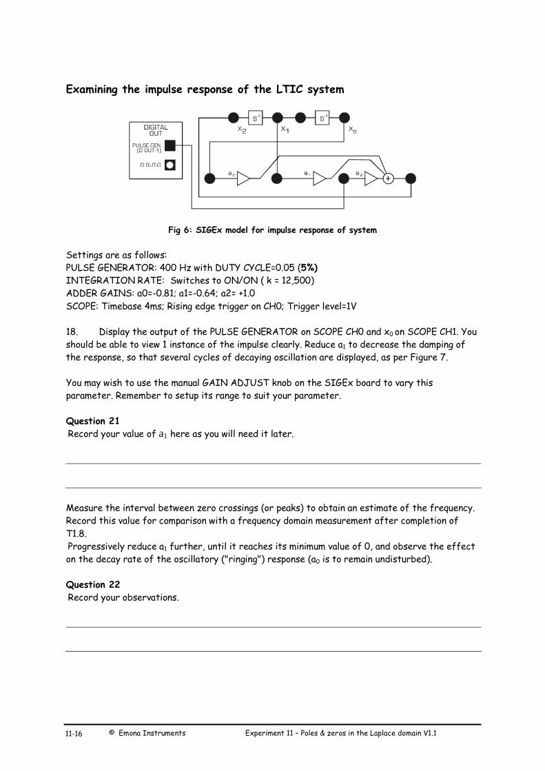
© Emona Instruments Experiment 11 – Poles & zeros in the Laplace domain V1.1 11-16
Examining the impulse response of the LTIC system
Fig 6: SIGEx model for impulse response of system
Settings are as follows: PULSE GENERATOR: 400 Hz with DUTY CYCLE=0.05 (5%) INTEGRATION RATE: Switches to ON/ON ( k = 12,500) ADDER GAINS: a0=-0.81; a1=-0.64; a2= +1.0 SCOPE: Timebase 4ms; Rising edge trigger on CH0; Trigger level=1V 18. Display the output of the PULSE GENERATOR on SCOPE CH0 and x0 on SCOPE CH1. You should be able to view 1 instance of the impulse clearly. Reduce a1 to decrease the damping of the response, so that several cycles of decaying oscillation are displayed, as per Figure 7. You may wish to use the manual GAIN ADJUST knob on the SIGEx board to vary this parameter. Remember to setup its range to suit your parameter. Question 21 Record your value of a1 here as you will need it later.
Measure the interval between zero crossings (or peaks) to obtain an estimate of the frequency. Record this value for comparison with a frequency domain measurement after completion of T1.8. Progressively reduce a1 further, until it reaches its minimum value of 0, and observe the effect on the decay rate of the oscillatory ("ringing") response (a0 is to remain undisturbed). Question 22 Record your observations.

Experiment 11 – Poles & zeros in the Laplace domain © Emona Instruments 11-17
Fig 7: impulse response of system for reduced a1 coefficient
If slowly decaying ringing is still present with the a1 level set to 0, continue to slowly increase its value in a positive direction ie: positive gain. At some point the decaying oscillations will be replaced by sustained self oscillations. Confirm that these oscillations remain when the input is disconnected and measure the frequency. Question 23 Record your findings.
19. Measure the peak-to-peak amplitude (adjust the gain control of the scope as needed). Plot an approximate locus of the poles. Label the points at which any observations of interest occur in the shape of the response. Comment on the behaviour of the impulse response when the poles have positive real part. You may find that the onset of instability does not occur exactly at the value of a1 that you would expect from theory. Consider practical issues that may cause this.

© Emona Instruments Experiment 11 – Poles & zeros in the Laplace domain V1.1 11-18
Graph 7: pole locus with varying a1 coefficient
Question 24 Return to the setup in Fig. 3 and with a0 back to the same position as in step 18, recorded in Q21, measure the resonance frequency at point x1 (the bandpass filter output). Compare this result with the time domain frequency measurements of the impulse response oscillations.

Experiment 11 – Poles & zeros in the Laplace domain © Emona Instruments 11-19
Part 2 – Feedback and feedforward In this Part we experiment with ideas introduced in prep items Q10-13. 20. Using the model of Fig. 3 that you patched up in Part 1, use the “b” ADDER on the SIGEx board to implement the feedforward gains b2, b1, b0 as follows: [b2, b1, b0] = [1, 0, 2] [a2, a1, a0 = [1, -0.64, -0.81] INTEGRATION RATE: DIPs set to UP:UP
x
2
x
1
x
0
-a
1
-a
0
b
b 0
b 1
2
b 2
y
u
Figure 8: schematic of 2nd order integrator feedback structure with feedforward combiner (from
preparation section of experiment)
Fig 9: SIGEx model of second order feedback system

© Emona Instruments Experiment 11 – Poles & zeros in the Laplace domain V1.1 11-20
21. Measure the gain response at y and compare with the results in prep Questions 10-12. Note that this response is lowpass. The zero at j1.41 produces a null at this frequency. Compare this response with the allpole response of x0 obtained in Part 1. In particular, examine the trade-off between depth of attenuation in the stopband and cut-off rate in the transition band. Confirm the frequency of the null. Plot the response on Graph 8.
Graph 8: response
Question 25 Decrease b0 progressively and observe that this causes a reduction of the gain at low frequencies. Continue until the gains at low and high frequencies are close to equal. You may wish to use the manual GAIN ADJUST knob on the SIGEx board to vary this parameter. Remember to setup its range to suit your parameter. Check that the null is still present. This realizes a bandstop filter, also known as a "notch" filter. Measure b0 (and a0 in case it was altered). Verify that b2 is still set to unity.

Experiment 11 – Poles & zeros in the Laplace domain © Emona Instruments 11-21
Question 26 Show that this response is obtained when b0 = a0 (with b2 = 1). This can be done quickly using Eqn 3 in prep Question 9: at low frequency, substitute s = 0; at high frequency use 1/s = 0.
Question 27 From prep Question 11 we expect the deepest notch when b1 is zero. Examine whether this is the case in your implementation. Vary b1 above and below zero and find the value that gives the deepest notch. Suggest why there may be a discrepancy between theory and practice.
Check the integrator gain by comparing theoretical and measured values of the null frequency. Consider possible practical causes for any discrepancies.
Question 28 Select a different integrator constant: suggested dip switch position DOWN UP (i.e k around 29,000/s) and measure the new null frequency.

© Emona Instruments Experiment 11 – Poles & zeros in the Laplace domain V1.1 11-22
The ALLPASS circuit 22. Using the same model of Fig.8 that you patched up in Part 2, restore the ADDER gains as follows: [b2, b1, b0] = [1, 0, 2] [a2, a1, a0 = [1, -0.64, -0.81] INTEGRATION RATE: DIPs set to UP:UP Gradually vary the b1 value from 0 in a negative direction and observe the depth of the notch decrease. Continue until there is no dip. Carefully trim b1 for a response that is flat across the entire frequency range. You may wish to use the manual GAIN ADJUST knob on the SIGEx board to vary this parameter. Theoretically, the condition for this response ("allpass") is b1 = a1 (with b0 = a0 and b2 = 1). Suggest why the theoretical condition may not be satisfied in the hardware if there are discrepancies. Plot the poles and zeros and show graphically that the magnitude response is allpass (refer to prep item Q13), on Graph 9. Question 29 Measure and plot the phase shift vs frequency and, again compare with your expectations from the pole-zero plot, on Graph 9.
Graph 8:allpass responses

Experiment 11 – Poles & zeros in the Laplace domain © Emona Instruments 11-23
Viewing frequency responses using FFT Having measured several responses by taking individual single frequency measurements, you can understand that it is worthwhile implementing a more automated methodology for viewing system responses across a spectral range. By using a multi-frequency input signal one can view the output of a system with an FFT display and see the complete frequency response of the system. A suitable input signal is a pseudo-noise signal with a flat spectrum at the frequencies of interest. This signal was investigated in a previous experiment (Experiment 9) and so will not be discussed in detail here.
Figure 10: example output spectrums for feedback and feedforward system
with multi-frequency input signal 23. Patch together the input noise signal as shown in Figure 11 and view the output of the system with the scope, by using the scopes FFT display. Settings are as follows: PULSE GENERATOR: Frequency = 30kHz, Duty cycle=0.5 (50%) TUNEABLE LPF: Corner frequency set to approx. 3kHz SCOPE: Timebase : 100ms
Figure 11: SIGEx model for a multi-frequency, flat spectrum signal source. TUNEABLE LPF Fc generally set to 10-15% of CLK frequency for flat response
24. Repeat several of the previous exercises with this method and compare your observations with your previous findings. You will find the exercises involving the use of the

© Emona Instruments Experiment 11 – Poles & zeros in the Laplace domain V1.1 11-24
GAIN ADJUST knob to be particularly interesting and dynamic, as you can explore the interaction of parameters in real time. Switch to TAB “ZOOM FFT” for a more detailed display of the time & frequency domains.
Part 3 – Critical damping & maximal flatness You may have come across the terms "maximally flat" and "critically damped". To explore these ideas we return to the allpoles lowpass filter used in Part 1. Although the feedforward subsystem is not required, there is no need to alter the setup you have been using in Part 2 as we will be ignoring the feedforward output. Notice that the feedforward section has no impact on the performance of the feedback section. 25. Set the “a” ADDER gains as for Part 1 of this experiment, as follows: [a2, a1, a0] = [1, -0.64, -0.81]. Display the lowpass output x0, and carry out a quick scan of the gain response with the FUNCTION GENERATOR set to a sinewave output. Note the significant overshoot at the high end of the passband. Gradually vary the a1 gain control and watch the reduction in overshoot. Continue until the overshoot is barely observable. Don't forget to check for any variation of input amplitude that may affect your observations. Question 30 Record the values of a0 and a1 that realize this outcome. This response is known as maximally flat. In Tut Q.8 you are invited to show that the formula for a maximally flat second order allpole is a1 = √(2.a0).
26. Critical damping is a condition that pertains to the step response. To generate a step response we use a low frequency squarewave as input from the PULSE GENERATOR. Settings are as follows: PULSE GENERATOR: 400 Hz with DUTY CYCLE=0.5 (50%) INTEGRATION RATE: Switches to ON/ON ( k = 12,500) ADDER GAINS: a0=-0.81; a1=-0.64; a2= +1.0 SCOPE: Timebase 400us/div; Rising edge trigger on CH0; Trigger level=1V Display x0 and the input squarewave and observe the overshoot in x0. Progressively increase a1 until the overshoot is barely observable. You may wish to use the manual GAIN ADJUST knob on the SIGEx board to vary this parameter. Remember to setup its range to suit your parameter.

Experiment 11 – Poles & zeros in the Laplace domain © Emona Instruments 11-25
Figure 12: example underdamped and critically damped step responses
Question 31 Record the values of a0 and a1 that realize this outcome. This response is known as critically damped. It is of interest in control systems as it realizes the most rapid risetime without overshoot. This idea also finds application in the context of Gaussian filters. Further exploration of critical damping is provided in Tut. Q.9.

© Emona Instruments Experiment 11 – Poles & zeros in the Laplace domain V1.1 11-26
Tutorial questions
Q1 From prep item (c): determine the position of the pole p1 in terms of the coefficients a0 and a1, i.e., show that with p1 expressed in polar form p1 = ρ.exp(j.θ), we have
ρ = sqrt(a0) and cos(θ) = a1/2 ρ
Q2 Allpole bandpass filter: a. Derive the transfer function and squared magnitude response formula for the second
order resonator in Fig. 1. Obtain the conditions for the poles to be complex valued; show this graphically, i.e., on a plane with axes a0 and a1.
b. Show that there is a magnitude response peak at w0=sqrt(a0) (hint: save time and effort: use the reciprocal of the response formula; manipulate this to reveal a simple and quick method without differentiation!). c. In the Lab you discovered that a0 tunes the resonance frequency, and a1 controls the bandwidth with almost no interaction. Confirm this serendipitous property analytically (hint: the result in part a of this question). d. Derive the 3dB points and show that the bandwidth is given by a1(subject to conditions for complex poles being satisfied). Show that the product of the 3dB frequencies is equal to the square of the resonance frequency w0 (i.e.,equal to a0). Hint: inspect the simple formula that revealed the peak. Look for terms of the form (w – 1/w)2 e. Apply these results to the measurements in T1.4.
Q3 State the coefficient conditions to realize an allpass. It would be useful to have an allpass realization in which the values of a0 and b0, and of a1 and b1 are implemented by single controls, respectively. Show how Fig 2 can be modified to achieve this. Indicate a possible practical difficulty with this idea (Hint: refer to your findings in T2.7).
Q4 Obtain the theoretical phase and group delay responses for the allpass in T2.7. Q5 As mentioned in T2.6, switched-capacitance filters (SCF) are used in the SIGEx TUNEABLE LOWPASS FILTER. Find out how this works and explain how the tuning is implemented in this module.
Q6 What is an elliptic filter? Explain how to use the structure in Fig 2 to implement elliptic filters. What is the required value of b1? Q7 Show how the system in Fig. 2 can be used to implement a tuneable notch with a single tuning control. Indicate applications of notch filters Q8 Derive the conditions for a maximally flat allpole 2nd order LPF (i.e., transfer function, and poles). Q9 Derive conditions for critical damping; does critical damping of the impulse response occur at the same pole values as for step response? Q10 (optional) In this exercise we consider the application of poles and zeros in the design of a fourth order BPF as a cascade of two biquad sections (Fig. 2). Suppose a centre frequency of 0.9 rad/s is specified. The design is to provide two zeros on the j axis, one above the passband, one below.

Experiment 11 – Poles & zeros in the Laplace domain © Emona Instruments 11-27
a. Plot a suitable pole zero constellation. Estimate the pole positions so that the bandwidth is around 0.1 rad/s. To achieve a flat passband the poles should be slightly offset ("staggered "). Note that if they are too far apart, an excessively deep trough will result. To estimate the overall magnitude response, plot estimates of the individual biquad responses on a dB gain scale. Use the results obtained in T2.2 as a guide. Note that one section will be lowpass and the other highpass. Students with access to four LAPLACE modules are encouraged to try this at the lab bench. You will find it very helpful to exploit the orthogonality of a0 and a1 (see Q2) as you trim your design. Adjust the placement of the zeros to achieve a practical balance between width of transition bands and depth of attenuation in the stopbands. b. Note that there are two pole zero pairings available, low pole with high zero, and viceversa. The usual criterion for the choice is dynamic range, ie. avoiding large peaks. Which is the best pairing? c. Suppose the specification had called for a bandwidth of 0.02 rad/s. Consider the practical challenges faced by the designer. One of these is dynamic range at internal nodes. Estimate the selectivity that could be realistically achieved with SIGEx LAPLACE modules using the structure in Fig 2. Indicate your reasons. Other biquad structures are available for consideration. These can be found in standard textbooks. d. Show a fourth-order system realized as a single stage of the form of Fig. 2. List practical issues that should be considered in comparing an implementation of the above filter as a single stage versus cascaded biquads.

© Emona Instruments Experiment 11 – Poles & zeros in the Laplace domain V1.1 11-28


© Emona Instruments Experiment 15 – Poles and Zeros in the z plane V1.1 15-2
Experiment 15 – Poles and zeros in the z plane: IIR systems
Achievements in this experiment
You will be able to interpret the poles and zeros of the transfer function of discrete-time filters to visualize frequency responses graphically at a glance, without math. You will be able to use this knowledge to intuitively design recursive/IIR discrete-time responses.
Preliminary discussion In Lab 11 we discovered how poles and zeros can be used as an intuitive tool for analyzing and designing continuous-time (CT) filters. Next, in Lab 14 we examined discrete-time (DT) FIR filters and found the same ideas could be applied there. The complex "s" plane was replaced with the complex "z" plane, and the unit circle used instead of the j axis for the representation of frequency. Because zeros only are involved in FIR filter work, this provided a convenient gateway to getting started with z-plane ideas. In this Lab we will investigate more general DT filters that are characterized with both poles and zeros. These filters are known as recursive since they use feedback, and also as Infinite Impulse Response (IIR). With feedback we will be able to realize much higher selectivity than possible with a comparable complexity FIR implementation. The most conspicuous example is the second-order resonator, which will open the way to achieving realistic bandpass responses. As we proceed, we will find many parallels with the CT(continuous time) filter experiments in Lab 11.
Part 1: we examine the behaviour of the basic second-order resonator implemented without zeros. Part 2: zeros are introduced to generate lowpass, bandpass, highpass and allpass responses using the Direct Form 2 structure.

Experiment 15 – Poles and Zeros in the z plane © Emona Instruments 15-3
Pre-requisite work:
This preparation extends the theory covered in Lab 14 to include poles.
UNIT DELAY T
INPUT
u
x 1 x 2 x
0
-a 1
-a 2
UNIT DELAY T
Figure 1: schematic of 2nd-order feedback structure without feedforward.
Question 1
Consider the feedback system in Figure 1. Show that the difference equation relating the adder output x0(nT) and the input u(nT) is x0(nT) = u[nT] - a1.x0[(n - 1)T] - a2.x0[(n - 2)T] (Eqn 1), where nT are the discrete time points, T sec denoting the unit delay, i.e. the time between samples. Show by substitution that ejnTw is a solution, i.e. show that when x0(nT) is of the form e
jnTw, the input u(nT) is ejnTw, multiplied by a constant (complex-valued); w is the frequency of the input in radians/sec; (the use of complex exponentials for the representation of sinusoidal signals is discussed in Lab 8, 10 and 13. From the above, with input u(nT) = ejnTw obtain x0/u = 1/[ 1 + a1. e
-jTw + a2. e-j2Tw] (Eqn 2).
Note that x0/u is not a function of the time index n.
Question 2
Use this result to obtain a general expression for |x0/u| as a function of w. Tip: to simplify the math, operate on u/x0 instead of x0/u, expressing the result in polar notation.

© Emona Instruments Experiment 15 – Poles and Zeros in the z plane V1.1 15-4
Set T = 1 sec for the time being, and plot the result for the case a1 = -1.6 , a2 = 0.902 over the range w = 0 to π rad/sec. Label the frequency axis in Hz and in rad/sec. You should find there is a peak in the response near 0.09Hz.
Graph 1:response plot
Question 3 Replace "exp(jTw)" by the symbol "z" in Eqn 2. The result is H_x0(z) = x0/u = 1/(1 + a1.z
-1 + a2.z-2 ) = z2 / ( z2 + a1.z + a2 ) (Eqn 3).
The quadratic ( z2 + a1.z + a2 ) can be expressed in the factored form (z - p1)(z - p2).

Experiment 15 – Poles and Zeros in the z plane © Emona Instruments 15-5
Figure 2: Notes on the graphical interpretation of pole-zero plots

© Emona Instruments Experiment 15 – Poles and Zeros in the z plane V1.1 15-6
Reviewing the finding of roots of the quadratic polynomial
From equation 1 above x0(nT) = u[nT] - a1.x1(nT) - a2.x2(nT) substituting x1=x0.z
-1 and x2=x0.z-1.z-1 we arrive at
x0 = u –a1x0/z1 – a2x0/z
2 Grouping x0 terms: x0(1 + a1/z
1 + a2/z2) = u
At this point we can see that although we started with negative gains in the circuit model, we now have positive values as coefficients in the quadratic equation. Further, we arrive at: x0/u = z
2/(z2 + a1z1 + a2) which we earlier named Eqn 3.
We now have the general quadratic form with positive coefficients. INSIGHT: positive coefficients result in negative gains in the actual implementation This quadratic (z2 + a1z + a2) can be expressed in factored form, as (z-p1)(z-p2) Remember that z, p1 & p2 are complex numbers. You can think of these as vectors: from the origin of the z plane to a 2 dimensional point on that plane. Each factor ie: (z-p1) and (z-p2) is a difference vector between a general point z, who’s locus we restrain to the unit circle, and the 2 specific roots p1 & p2. It will be a vector, having direction and magnitude, and can be expressed in polar notation as r⁄θ, or rejθ, or in Cartesian notation as (a + ib). Both these representation are complex numbers. If we define p1 as (σ + iw) and its conjugate, p2 as (σ – iw) we can express the quadratic factors as: (z- p1)(z- *p1) = z2 + p.*p – pz – *pz Switching to polar notation for convenience, p.*p = rejθ. re-jθ = r2 So that leaves z2 + r2 –z.(p + *p), and if using Cartesian notation in this instance for convenience, ie. p = σ + jw then p + *p = 2σ so z2 +(-2 σ)z + r2 = z2 -2 σ z + r2 = z2 +a1z + a2 Relating coefficients gives a1 = -2σ and a2 = r
2 For stability the poles must always be inside the unit circle, hence 0 < a2 < 1 Changes in a1 directly influence the real component of the pole position a2 has a square law relationship with r of the pole. Other relationships, such as θ, w, imag part, can be derived from these easily with trigonometry. The general solution for the roots of the quadratic polynomial x2 + a1x + a2 is: x = -a1/2 +/- i√[a2-(a1/2)
2]
With these equations in mind consider how changes in the coefficients from the math will move the poles or zeros about the unit circle, and influence the response of the system. This lab aims to make you more familiar of the interrelationships between these parameters.

Experiment 15 – Poles and Zeros in the z plane © Emona Instruments 15-7
Using the values of a1 and a2 given in Question 2 above, find the roots p1 and p2 (express the result in polar notation). Mark the position of p1 and p2 on the complex z plane with an "x" to indicate that they represent poles. The distance between these points and the unit circle is of key importance. This is a parallel process to that in Lab 11 where we plotted zeros. A similar procedure was carried out in Lab 11 for a CT transfer function in the complex variable s. Write down a formula for p1 in terms of a1 and a2. Note that p1 may be real or complex depending on a1 and a2. Determine the conditions for p1 to be complex valued. For this case, express p1 in polar notation. Take note of the fact that |p1| does not depend on a1 (this will be useful later). Obtain p2 from p1.
Question 4
Satisfy yourself that the magnitude response of H_x0 is given by |H_x0(w)| = 1/[|(e
jTw - p1)|.|(expjTw - p2)|] (Eqn 4).
This provides the key for the graphical method described in Lab 13 to obtain an estimate of the magnitude response. Again, we will use T = 1 . Plot the magnitude of the denominator for selected values of w over the range 0 to π. The quantity |(ejTw - p1)| becomes quite small and changes rapidly as the point on the unit circle is moved near p1. Plot additional points there as needed. Invert to get |H_x0(w)| and compare this with the result you obtained in (b).

© Emona Instruments Experiment 15 – Poles and Zeros in the z plane V1.1 15-8
Graph 2:response plot
x
2
x
1
x
0
-a
2
-a
1
b 0
b 1
b 2 y
u 1 / Z 1 / Z
Figure 3: block diagram of 2nd-order Direct-form 2 structure with feedforward.

Experiment 15 – Poles and Zeros in the z plane © Emona Instruments 15-9
Question 5
Modify Fig 1 by replacing the unit delays with a gain of 1/z and show that Eqn 3 follows by inspection using simple algebra.
Question 6
Apply this idea to show that the transfer function for the system in Fig. 3 is H_y (z) = y/u = (b0 + b1.z
-1 + b2.z-2 ) /(1 + a1.z
-1 + a2.z-2 ) (Eqn5)
Question 7
Use the graphical pole-zero method (covered in Experiment 14) to obtain estimates of the magnitude responses for the following cases (0 to Nyquist freq): (i) b0 =b2 = 1, b1 = 2, a1 and a2 as in Question 2. (ii) b0 = b2 = 1, b1 = - 2, a1 and a2 as in Question 2 (iii) b0 = 1, b1 = 0, b2 = - 1, a1 and a2 as in Question 2
Which of these is lowpass, highpass, bandpass?

© Emona Instruments Experiment 15 – Poles and Zeros in the z plane V1.1 15-10
Graph 3:pole-zero method
Question 8
Consider a DT system with sampling rate 20kHz. Obtain estimates of the poles and zeros that realize a lowpass filter with cut-off near 3kHz. Obtain a highpass filter using the same poles.
Question 9
For the same sampling rate as in Question 8 obtain estimates of the poles and zeros that realize a bandpass filter centered near 3.1kHz, with 3dB bandwidth 500Hz. HINT: review Question 7

Experiment 15 – Poles and Zeros in the z plane © Emona Instruments 15-11
Equipment
� PC with LabVIEW 2009 (or higher) & “Digital Filter Design” toolkit installed
� NI ELVIS 2 or 2+ and USB cable to suit
� EMONA SIGEx Signal & Systems add-on board
� Assorted patch leads
� Two BNC – 2mm leads
Procedure
Part A – Setting up the NI ELVIS/SIGEx bundle
1. Turn off the NI ELVIS unit and its Prototyping Board switch. 2. Plug the SIGEx board into the NI ELVIS unit. Note: This may already have been done for you. 3. Connect the NI ELVIS to the PC using the USB cable. 4. Turn on the PC (if not on already) and wait for it to fully boot up (so that it’s ready to connect to external USB devices). 5. Turn on the NI ELVIS unit but not the Prototyping Board switch yet. You should observe the USB light turn on (top right corner of ELVIS unit).The PC may make a sound to indicate that the ELVIS unit has been detected if the speakers are activated. 6. Turn on the NI ELVIS Prototyping Board switch to power the SIGEx board. Check that all three power LEDs are on. If not call the instructor for assistance. 7. Launch the SIGEx Main VI. 8. When you’re asked to select a device number, enter the number that corresponds with the NI ELVIS that you’re using. 9. You’re now ready to work with the NI ELVIS/SIGEx bundle. 10. Select the EXPT 15 tab on the SIGEx SFP. Note: To stop the SIGEx VI when you’ve finished the experiment, it’s preferable to use the STOP button on the SIGEx SFP itself rather than the LabVIEW window STOP button at the top of the window. This will allow the program to conduct an orderly shutdown and close the various DAQmx channels it has opened.
Ask the instructor to checkyour work before continuing.

© Emona Instruments Experiment 15 – Poles and Zeros in the z plane V1.1 15-12
Experiment
Part 1: IIR without feedforward: a second-order resonator In this part we implement and investigate the system in Fig 1.
Figure 4: patching diagram for feedback structure without feedforward from Figure 1
11. Patch up a SIGEx model of the system in Fig 1. Settings are as follows: ADDER GAINS: a0=1; a1=+1.6; a2= -0.902 PULSE GENERATOR: 20kHz, DUTY CYCLE=0.5 (50%) FUNCTION GENERATOR: Sinewave selected, FREQUENCY=1k; Amplitude= 2V pp SCOPE: Timebase = 4ms, Trigger on input signal, Trigger level = 0V Question 10
Calculate the poles corresponding to these values. Measure and plot the magnitude response at the output of the feedback adder. Note and record the resonance frequency and the bandwidth. Use the poles to graphically predict these parameters; compare with your measurements.
HINT: Do a quick sweep of frequency range, and turn AUTOSCALE off at maximum amplitude, then sweep the range more slowly while taking measurements. This will enable you to see the variation in gain of the output more easily than with AUTOSCALE on. Question 11
Decrease |a1| by a small amount ( around 5-10%, say) and measure the effect on the resonance frequency and bandwidth. Use this to estimate the migration of the poles. Does this agree with your expectations?
Question 12

Experiment 15 – Poles and Zeros in the z plane © Emona Instruments 15-13
Repeat step 3 for a 5% decrease of a2. Compare the effects of varying a1 and a2. Which of these controls would you use to tune the resonance frequency? Use the formulas you obtained in the preparation to explain this.
NOTE about TAB “ PZ plot” on the SIGEx SFP.
This panel calculates the poles and zeros relating to the currently set ADDER gains which relate to the coefficients of the transfer function. Use this visualization tool to confirm your understanding . You may wish to move back and forth between the experiment TAB and the “PZ plot” TAB as required during the experiment.
Figure 5: “PZ plot” TAB from SIGEx SFP
You may wish to use the manual GAIN ADJUST knob on the SIGEx board to vary these parameters. Remember to setup its range to suit your parameter. Question 13
With a1 unchanged, gradually increase a2 and observe the narrowing of the resonance. Continue until you see indications of unstable behaviour. At that point, remove the input signal and observe the output (if needed, increase a2 a little more). Is it sinusoidal? Measure and record its frequency. Measure a2. Calculate and plot the pole positions. Note especially whether they are inside or outside the unit circle.

© Emona Instruments Experiment 15 – Poles and Zeros in the z plane V1.1 15-14
Figure 6: patching diagram for step response
12. We will now repeat step 11 in the time domain. Use the PULSE GENERATOR as a clock source and SEQUENCE GENERATOR to set up a unit pulse input. The SYNC signal from the SEQUENCE GENERATOR will act as a repetitive unit pulse source. What matters is that the unit pulses are far enough apart that each pulse is a unique event to the system under investigation. Setting are as follows: PULSE GENERATOR: 20kHz, DUTY CYCLE=0.5 SEQUENCE GENERATOR: DIPS set to UP:UP (short sequence) ADDER gains: a0=1.0; a1=1.6; a2=-0.902; b0=1.0 Question 14
Begin with a2 around -0.9. Describe the effect on the response as the magnitude of a2 reduces. Measure the frequency of the oscillatory tail of the response and compare with your observations in step 5.
Figure 7: typical pulse response

Experiment 15 – Poles and Zeros in the z plane © Emona Instruments 15-15
Graph 4:pole only response plot
Figure 8: Setup with feedforward and feedback sections implemented, as per Figure 9 below

© Emona Instruments Experiment 15 – Poles and Zeros in the z plane V1.1 15-16
Part 2 - IIR with feedforward: second-order filters In this part we implement and investigate the system in Fig 9. Note that the system with feedforward simply builds upon the previous system with feedback only. It also provides a new output point. The system response x0 for the feedback only, all-pole system is still available as a subset within this new arrangement and is unchanged by the additional feedforward elements. The feedforward elements simply add numerator terms to the overall transfer function which becomes y/u.
x
2
x
1
x
0
-a
2
-a
1
b 0
b 1
b 2 y
u 1 / Z 1 / Z
Figure 9: block diagram of 2nd-order Direct-form 2 structure with feedforward.
13. Use ADDER B in a z-TRANSFORM module to convert the SIGEx model of Part 1 to the system in Fig 9.
Figure 10: patching diagram for block diagram above
14. Implement case (i) in Prep (Q7). Settings are as follows: ADDER GAINS: b0=1; b1=2; b2=1; a0=1; a1=+1.6; a2= -0.902 PULSE GENERATOR: 20kHz, DUTY CYCLE=0.5 (50%) FUNCTION GENERATOR: Sinewave selected, FREQUENCY=1k; Amplitude= 1V pp

Experiment 15 – Poles and Zeros in the z plane © Emona Instruments 15-17
SCOPE: Timebase = 4ms, Trigger level = 0V, Trigger on input signal
Figure 11: Using the Function Generator to sweep a sinusoid across the spectrum of interest.
Observation: the high pass band gain due to the selection of coefficients resulting in poles very close to the unit circle, as shown in the figure below.
Figure 12: details of the PZ PLOT TAB for the current settings
(NB: 2 zeros at (-1 +/- 0i) are difficult to see in figure.)
NOTE: The poles are very close to the unit circle. In fact, the pole radius is 0.95. Hence the gain close to the poles is very large. You can use the PZ PLOT to visualize the poles and zeros for any “live” coefficient settings. Zeros are also present at z = -1.

© Emona Instruments Experiment 15 – Poles and Zeros in the z plane V1.1 15-18
Measure the magnitude response |y/u| and confirm that it is a lowpass filter.
Graph 5: plot of responses
Question 15
In the model of step 14, adjust a2 to reduce the peaking to a minimum. As well you will need to reduce the amplitude of the input signal to 0.5Vpp to reduce saturation. Confirm this for yourself. Plot the resulting response and measure the new value of a2. Calculate and plot the new poles. Obtain an estimate of the theoretical magnitude response with these poles and compare this with the measured curve. Why was a2 used for this rather than a1?
Question 16
Change the polarity of b1 in the lowpass of step 19 and show that this produces a highpass. Compare with your findings in Question 7.

Experiment 15 – Poles and Zeros in the z plane © Emona Instruments 15-19
NOTE: the following three questions refer to the transfer function coefficient values. Remember to negate the a1 and a2 values when settings them up as ADDER GAINS. Question 17
Repeat for case (iii) in Question 7, that is: b0 = 1, b1 = 0; b2 = -1 ; a0 = 1; a1 =-1.6; a2 =0.902; Confirm this is a bandpass filter. Tune a1 and a2 to obtain a peak at 3.1 kHz and 3dB bandwidth 500Hz. Measure the resulting a1 and a2 and plot the new poles. Compare this with your findings in Question 7.
Question 18
Implement the following case: a0 = 1, a1 = 0, a2 = 0.8, b0 = 0.8, b1 = 0, b2 = 1. Note that b0=a2 and b1=a1. Measure the magnitude response. Confirm it is allpass. Locate the positions of the poles and zeros. Plot them below for your records.
Question 19
Change a1 and b1 to - 1.6 and confirm the response is still allpass. Examine the behaviour of the phase response. Look for the frequency of most rapid phase variation, and confirm this occurs near a pole. Plot the poles and zeros below for your records.

© Emona Instruments Experiment 15 – Poles and Zeros in the z plane V1.1 15-20
Viewing spectrum of system with broadband noise input & FFT
As well as sweeping a single frequency signal from the FUNCTION GENERATOR across the spectrum of interest it is also convenient to input a broad range of frequencies at once and view the overall output frequency response of the system. Creating a broadband analog noise signal was covered in Experiment 9. That methodology is shown in the figures below. You can revisit this experiment with this setup in place and see the relationships of poles and zeros to system response in real time.
Figure 13: IIR filter with flat noise input
Figure 14: experiment setup with noise input signal instead of Function Generator signal. Uses
SEQUENCE GENERATOR and TUNEABLE LPF, clocked from PULSE GENERATOR.

Experiment 15 – Poles and Zeros in the z plane © Emona Instruments 15-21
15. Ensure that SEQUENCE GENERATOR DIP switches are set to positions DOWN:DOWN for the long sequence. Set TLPF knobs to fully clockwise for now. Switch to TAB “ZOOM FFT” to view time and frequency domains simultaneously. Change scope timebase to 100ms. Set up the coefficients as per step 14. Setting up the input noise signal: 16. i) Reduce the TLPF GAIN by rotating counter clockwise until the output Ch1 signal (red) is no longer saturated ie: less than 12V peak. ii) Reduce the noise bandwidth to around 4khz by rotating the TLPF block’s “Fc” control-counter clockwise. View the noise spectrum as the white trace on the SCOPE & FFT windows. The SFP should be similar to Figure 15 below for a peaky LPF as shown.
Figure 15: ZOOM FFT TAB used to view Experiment 15 setup with flat noise input.
Due to high gain, input noise level is very small. Note the limited bandwidth of the input noise to maintain a flat input response. (SEQUENCE GENERATOR must be set to long sequence.) At this point we can see and explore the issues relating to : -controlling our input signal level and bandwidth -viewing the response in both time and frequency domains -setting up a transfer function with appropriate internal gains We can also confirm that the peak of the response is correct according to the position of the poles. ie: PZ PLOT tells us that poles are at 32 degrees, hence we expect a peak close to 32/360*20,000 = 1777 Hz. You can use the cursors in ZOOM FFT window to confirm this.

© Emona Instruments Experiment 15 – Poles and Zeros in the z plane V1.1 15-22
Question 20
Show your calculation of the where you expect the peak frequency to be using the pole position and sampling frequency.
Dynamically varying the poles and zeros to adjust response using GAIN
ADJUST manual control 17. Use the SIGEx board’s GAIN ADJUST knob to vary one of the coefficients by hand while viewing the frequency response. Leave the default settings. Turn the knob until it reads +1.6 (located in the COEFFICIENT SELECTOR window), then select radio button “ a1 ”. View the frequency response while slowly varying the value of a1. You will find that the peak frequency changes. 18. Find a range of a1 settings that work well and then view PZ PLOT while varying across that range. You will see the poles moving and reflecting the changing a1 coefficient. (Theory states that a1=-2σ, which is the real part of the pole and its conjugate.) Question 21
Confirm this relationship from values displayed on PZ PLOT and show your working here:
19. Set a1 back to +1.6, select OFF, then set GAIN ADJUST to -0.9, and select a2 radio button. For more resolution vary the setup parameters as required. Question 22
Varying a2 will vary the gain or peak level of the filter. Notice what happens in the time domain when a2 = -1.0. The filter breaks into oscillation. View the poles again using PZ PLOT while varying a2. (Theory states that a2 = r
2).
20. Set a2 back to -0.9, then select OFF again at the COEFFICIENT SELECTOR to disable the GAIN ADJUST control.
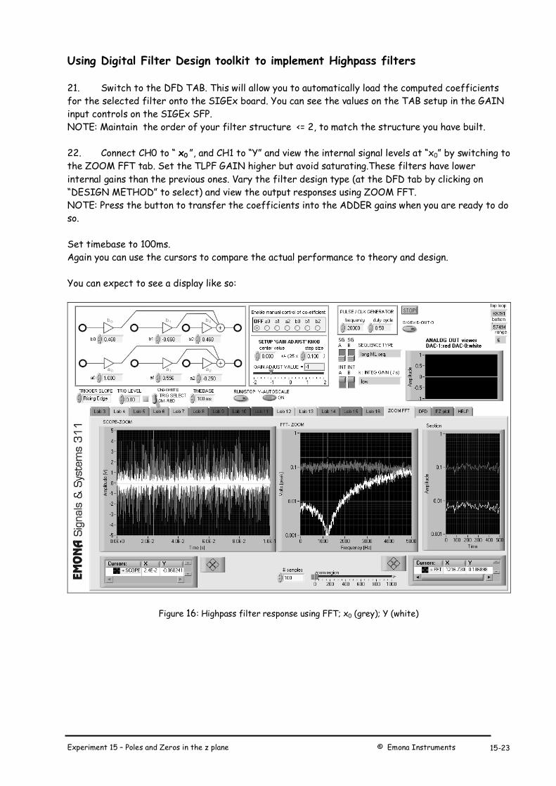
Experiment 15 – Poles and Zeros in the z plane © Emona Instruments 15-23
Using Digital Filter Design toolkit to implement Highpass filters 21. Switch to the DFD TAB. This will allow you to automatically load the computed coefficients for the selected filter onto the SIGEx board. You can see the values on the TAB setup in the GAIN input controls on the SIGEx SFP. NOTE: Maintain the order of your filter structure <= 2, to match the structure you have built. 22. Connect CH0 to “ x0 ”, and CH1 to “Y” and view the internal signal levels at “x0” by switching to the ZOOM FFT tab. Set the TLPF GAIN higher but avoid saturating.These filters have lower internal gains than the previous ones. Vary the filter design type (at the DFD tab by clicking on “DESIGN METHOD” to select) and view the output responses using ZOOM FFT. NOTE: Press the button to transfer the coefficients into the ADDER gains when you are ready to do so. Set timebase to 100ms. Again you can use the cursors to compare the actual performance to theory and design. You can expect to see a display like so:
Figure 16: Highpass filter response using FFT; x0 (grey); Y (white)

© Emona Instruments Experiment 15 – Poles and Zeros in the z plane V1.1 15-24
Figure 17: DFD TAB used to design filters and setup coefficients to the patched SIGEx board
Default values are chosen to enable students to see textbook like responses which they can easily measure. Question 23
Confirm that the SIGEx hardware performs as designed by theory in terms of notch positions etc. You will have to use the zero positions mostly in these cases. Why ?
Notches are implemented by placement of zeros on or near the unit circle.
Question 24
Try varying design values and take note of the ORDER of the filter designed. NOTE that the SIGEx experiment we have implemented can only support a 2nd order structure. Note your observations.

Experiment 15 – Poles and Zeros in the z plane © Emona Instruments 15-25
Tutorial Questions
Q1. Why do the complex poles and zeros occur in conjugate pairs in the cases covered in this lab?
Q2. Why is polar notation for complex valued poles and zeros preferred in the discrete-time context? Using examples from the lab, explain the importance of the position of complex poles/zeros relative to the unit circle when estimating frequency responses.
Q3. Re Eqn 3, keeping a1 constant, plot the locus of the upper half plane pole with respect to a2. Do this for several suitable values of a1. Holding a2 constant, repeat this with respect to a1. Use the resulting contours to explain your observations in Q11 and Q12 .
Q4. Determine the conditions on a1 and a2 for the poles to be complex. Display this graphically on a plane (i.e. with a2 = 0 as horizontal axis and a1=0 as vertical axis).
Q5. Calculate and plot the poles and zeros in Q19. Satisfy yourself that they share the same radial line. Show that z1 = 1/p1* .
Q6. Prove that the values of the coefficients in Q18 and Q19 generate a constant magnitude response over all frequencies. Write down the coefficient relationship in the transfer function of a fourth-order allpass.
Q7. Consider the unit pulse response in Step 12. What is the effect on the decay rate as the bandwidth is decreased? Find a simple formula or rule of thumb to express this relationship.
Q8. Show that the magnitude responses at nodes x1 and at x2 are the same as at x0 (can be demonstrated without math).
Q9. Consider a bandpass filter realized with a2 = 0.98. What is the maximum deviation allowable in a2 to maintain a bandwidth tolerance of 5 percent?
Q10. Consider the following assertion: "Continuous-time filters can be considered as a limiting case of discrete-time filters, as the sampling frequency to bandwidth ratio gets very large". Hint: show that the poles and zeros migrate to the area near (1,0) as the Nyquist ratio increases and compare the shapes of the unit circle and of the j axis in that region.
Q11. Find out the meaning of the term "maximally flat". Is this description applicable to the filter produced in Q15 by reducing the value of a2?

© Emona Instruments Experiment 15 – Poles and Zeros in the z plane V1.1 15-26

Appendix A: SIGEx Lab to Textbook chapter table
This table aims to direct users to sections of relevant texts which contain theory and exercises
related to experiments currently documented and implemented with the SIGEx/NI ELVIS bundle.
Given that SIGEx is by design an open-ended modeling system it is possible to build many more
experiments than is currently documented.
Users will find that many exercises from the texts which are currently undocumented in this Lab
Manual can also be implemented directly with minimum extra documentation.
Students can easily be directed to implement exercises from texts on the SIGEx board once they
become familiar with the block diagram modeling approach to building experiments.
The texts which are currently referred to in this Appendix are:
Lathi.B.P. , “Signal processing & Linear Systems”, Oxford University Press
Oppenheim.A.V.,Wilsky.A.S., “Signals & Systems”, Prentice Hall, 2nd edition
Haykin, Van Veen, “Signals and Systems”, Wiley, 2nd edition
Ziemer.R.E,Tranter.W.H, Fannin.D.R, “Signals & Systems: Continuous and Discrete”, Prentice
Hall, 4th edition
Boulet.B.: “Fundamentals of Signals & Systems”, Thomson/Delmar Learning
McClellan.J.H, Schafer.R.W, Yoder.M.A, “DSP First”, Prentice Hall


Lathi.B.P. , “Signal processing & Linear Systems”, Oxford University Press
SIGEx Lab Manual Lathi: text book correlation
S1-03: Special signals – characteristics and
applications
1 Introduction to Signals and Systems
B.2 Sinusoids
2.4 System response to external input: zero-state response S1-04: Systems: Linear and non-linear 1 Introduction to Signals and Systems
S1-05: Unraveling convolution 9.4-1 Graphical procedure for the convolution sum
S1-06: Integration, convolution, correlation &
matched filters
2.4-1 The convolution integral
3.2 Signal comparison: Correlation
S1-07: Exploring complex numbers and
exponentials
B.1 Complex numbers
B.3-1 Monotonic exponentials
B.3-2 The exponentially varying sinusoid
S1-08: Build a Fourier series analyzer 3.4 Trigonometric fourier series
S1-09: Spectrum analysis of various signal types 4 Continuous-time signal analysis: The fourier transform
S1-10: Time domain analysis of an RC circuit 1.8 System model: Input-output description
S1-11: Poles and zeros in the Laplace domain 6 Continuous-time system analysis using the Laplace
transform
S1-12: Sampling and Aliasing 5 Sampling
8.3 Sampling continuous-time sinusoid and aliasing
S1-13: Getting started with analog-digital
conversion
5.1-3 Applications of the sampling theorem (Pulse code
modulation PCM)
S1-14: Discrete-time filters with FIR systems 11 Discrete-time system analysis using the z-transform
12.1 Frequency response of discrete-time systems
12.2 Frequency response from pole-zero location S1-15: Poles and zeros in the z plane with IIR
systems
12 Frequency response and digital filters
S1-16: Discrete-time filters – issues in practical
applications
Not covered


Oppenheim.A.V.,Wilsky.A.S., “Signals & Systems”, Prentice Hall, 2nd edition
SIGEx Lab Manual Oppenheim, text book correlation
S1-03: Special signals – characteristics and
applications
1 Signals and Systems
S1-04: Systems: Linear and non-linear 1 Signals and Systems
2 Linear time-invariant systems
S1-05: Unraveling convolution 2.1 Discrete-time LTI systems: The convolution sum
S1-06: Integration, convolution, correlation &
matched filters
2.2 Continuous-time LTI systems: The convolution integral
2 Linear time-invariant systems; Problem 2.67
S1-07: Exploring complex numbers and
exponentials
1 Signal and systems: Mathematical review
1.3 Exponentials and sinusoidal signals
S1-08: Build a Fourier series analyzer 3.3 Fourier series representation of continuous-time
periodic signals
S1-09: Spectrum analysis of various signal types 4.1.3 Examples of Continuous-Time Fourier transforms
S1-10: Time domain analysis of an RC circuit 3.10.1 A simple RC lowpass filter
3.10.2 A simple RC highpass filter
S1-11: Poles and zeros in the Laplace domain 9 The Laplace transform
9.4 Geometric evaluation of the Fourier transform from the
pole-zero plot S1-12: Sampling and Aliasing 7 Sampling
S1-13: Getting started with analog-digital
conversion
8.6.3 Digital Pulse-Amplitude (PAM) and Pulse-Code
modulation (PCM)
S1-14: Discrete-time filters with FIR systems 6.6 First-order and second-order discrete time systems
6.7.2 Examples of discrete-time nonrecursive filters
S1-15: Poles and zeros in the z plane with IIR
systems
10.4 Geometric evaluation of the Fourier transform from
the pole-zero plot
S1-16: Discrete-time filters – issues in practical
applications
Not covered


Haykin, Van Veen, “Signals and Systems”, Wiley, 2nd edition
SIGEx Lab Manual Haykin, Van Veen, text book correlation
S1-03: Special signals – characteristics and
applications
1.6 Elementary signals
S1-04: Systems: Linear and non-linear 1.8 Properties of systems
S1-05: Unraveling convolution 2.2 The convolution sum
S1-06: Integration, convolution, correlation &
matched filters
2.5 Convolution integral evaluation procedure
S1-07: Exploring complex numbers and
exponentials
1.6.3 Relation between sinusoidal and complex exponential
signals
A.2 Complex numbers S1-08: Build a Fourier series analyzer 3.5 Continuous-time periodic signals: The Fourier series
S1-09: Spectrum analysis of various signal types 4.2 Fourier Transform representations of Periodic signals
S1-10: Time domain analysis of an RC circuit 6.7 Laplace transform methods in circuit analysis
S1-11: Poles and zeros in the Laplace domain 6 Representing signals by using continuous-time complex
exponentials: the Laplace transform
6.13 Determining the Frequency response from poles & zeros
S1-12: Sampling and Aliasing 4.5 Sampling
4.6 Reconstruction of continuous-time signals from samples
S1-13: Getting started with analog-digital
conversion
4.6.3 A practical reconstruction: the zero order hold
5.2 Types of modulation (PCM)
S1-14: Discrete-time filters with FIR systems 7 Representing signals by using continuous-time complex
exponentials: the z- transform
8.9 Digital FIR filters
S1-15: Poles and zeros in the z plane with IIR
systems
7.8 Determining the Frequency response from poles & zeros
8.10 IIR Digital filters
S1-16: Discrete-time filters – issues in practical
applications
7.9 Computational structures for implementing discrete-
time LTI systems


Ziemer.R.E,Tranter.W.H, Fannin.D.R, “Signals & Systems : Continuous and Discrete”, Prentice Hall,
4th edition
SIGEx Lab Manual Ziemer, Tranter, Fannin, text book
correlation
S1-03: Special signals – characteristics and
applications
1-3 Signal models
S1-04: Systems: Linear and non-linear 2-2 Properties of systems
S1-05: Unraveling convolution 8-4 Difference equations and discrete-time systems;
Example 8-12 Discrete convolution
10-6 Convolution
S1-06: Integration, convolution, correlation &
matched filters
10-6 Energy spectral density and autocorrelation function
S1-07: Exploring complex numbers and
exponentials
1-3 Phasor signals and spectra
S1-08: Build a Fourier series analyzer 3-3 Obtaining trigonometric Fourier series representations
for periodic signals
3-4 The complex exponential Fourier series
S1-09: Spectrum analysis of various signal types 4.5 Fourier transform theorems
S1-10: Time domain analysis of an RC circuit 2-2:2-7 System modeling concepts
6-2 Network analysis using the Laplace transform
S1-11: Poles and zeros in the Laplace domain 6-4 Transfer functions
S1-12: Sampling and Aliasing 8-2 Sampling
8-2 Impulse-train sampling model
S1-13: Getting started with analog-digital
conversion
8-2 Quantizing and encoding
S1-14: Discrete-time filters with FIR systems 9-5 Design of finite-duration impulse response (FIR) digital
filters
S1-15: Poles and zeros in the z plane with IIR
systems
9-4 Infinite Impulse Response (IIR) filter design
S1-16: Discrete-time filters – issues in practical
applications
9-2 Structures of digital processors


Boulet.B.: “Fundamentals of Signals & Systems”, Thomson/Delmar Learning
SIGEx Lab Manual Boulet, text book correlation
S1-03: Special signals – characteristics and
applications
1 Elementary continuous-time and discrete-time signals and
systems
S1-04: Systems: Linear and non-linear 2 Linear Time-invariant systems
S1-05: Unraveling convolution 2 Discrete-time systems: The convolution sum
S1-06: Integration, convolution, correlation &
matched filters
2 The convolution integral
S1-07: Exploring complex numbers and
exponentials
1 Complex exponential signals
S1-08: Build a Fourier series analyzer 4 Determination of the Fourier series representation of a
continuous-time periodic signal
S1-09: Spectrum analysis of various signal types 4 Fourier series representation of periodic continuous-time
signals
S1-10: Time domain analysis of an RC circuit 9 Application of Laplace transform techniques to electric
circuit analysis
S1-11: Poles and zeros in the Laplace domain 6 Poles and zeros of rational Laplace transforms
S1-12: Sampling and Aliasing 15 Sampling systems
S1-13: Getting started with analog-digital
conversion
16 Modulation of a pulse-train carrier
15 Signal reconstruction
S1-14: Discrete-time filters with FIR systems 14 Geometric evaluation of the DTFT from the pole-zero
plot
S1-15: Poles and zeros in the z plane with IIR
systems
14 Infinite Impulse Response and Finite Impulse Response
filters
S1-16: Discrete-time filters – issues in practical
applications
Not covered


McClellan.J.H, Schafer.R.W, Yoder.M.A, “DSP First”, Prentice Hall
SIGEx Lab Manual “DSP First”, text book correlation
S1-03: Special signals – characteristics and
applications
1 Mathematical representation of signals
S1-04: Systems: Linear and non-linear 2 Thinking about systems
S1-05: Unraveling convolution 5.3.3 Convolution and FIR filters
S1-06: Integration, convolution, correlation &
matched filters
Not covered
S1-07: Exploring complex numbers and
exponentials
2.5 Complex exponentials and phasors
S1-08: Build a Fourier series analyzer 3.4.1 Fourier series analysis
S1-09: Spectrum analysis of various signal types 3 Spectrum representation
S1-10: Time domain analysis of an RC circuit Not covered
S1-11: Poles and zeros in the Laplace domain Not covered
S1-12: Sampling and Aliasing 4 Sampling and aliasing
S1-13: Getting started with analog-digital
conversion
4.4 Discrete to continuous conversion
S1-14: Discrete-time filters with FIR systems 5 FIR filters
S1-15: Poles and zeros in the z plane with IIR
systems
8 IIR filters
S1-16: Discrete-time filters – issues in practical
applications
8 IIR filters


Appendix B: Quickstart guide to using SIGEx
Using “Experiment 15–Poles and zeros in the z-plane” as a basis for
a demonstration of SIGEx
Achievements in this experiment
Students learn better when they can see the theory in action with real systems. You will be able to
visualize the effect of pole zero placement on the system response for the time and frequency
domain. You can confirm the theory and compare with real system performance. You can vary
parameters in real time and confirm your understanding. You will be able to develop knowledge to
intuitively design transfer function responses.
Firstly browse through the sample manual to see the breadth and depth of possible hands-on
laboratory work possible with the NI ELVIS/SIGEx bundle.
Equipment
� PC with LabVIEW 2009 (or higher) & “Digital Filter Design” toolkit installed
� NI ELVIS 2 or 2+ and USB cable to suit
� EMONA SIGEx Signal & Systems add-on board
� Assorted patch leads
� Two BNC – 2mm leads
Follow setup Procedure as listed on page 11 of Experiment 15 to run the SIGEx board. Reproduced
here:

Procedure
Part A – Setting up the NI ELVIS/SIGEx bundle
1. Turn off the NI ELVIS unit and its Prototyping Board switch.
2. Plug the SIGEx board into the NI ELVIS unit.
Note: This may already have been done for you.
3. Connect the NI ELVIS to the PC using the USB cable.
4. Turn on the PC (if not on already) and wait for it to fully boot up (so that it’s ready to
connect to external USB devices).
5. Turn on the NI ELVIS unit but not the Prototyping Board switch yet. You should observe
the USB light turn on (top right corner of ELVIS unit).The PC may make a sound to indicate that
the ELVIS unit has been detected if the speakers are activated.
6. Turn on the NI ELVIS Prototyping Board switch to power the SIGEx board. Check that all
three power LEDs are on.
7. Launch the SIGEx Main VI.
8. When you’re asked to select a device number, enter the number that corresponds with the
NI ELVIS that you’re using. You’re now ready to work with the NI ELVIS/SIGEx bundle.
9. Select the EXPT 15 tab on the SIGEx SFP.
Note: To stop the SIGEx VI when you’ve finished the experiment, it’s preferable to use the STOP
button on the SIGEx SFP itself rather than the LabVIEW window STOP button at the top of the
window. This will allow the program to conduct an orderly shutdown and close the various DAQmx
channels it has opened.
Part B – Setting up the experiment
Run “NI ELVISmx Instrument Launcher” and select the FGEN “ Function Generator”. Run it and
minimise the FGEN panel for now.
Viewing SIGEx SFP, select Lab 15, which relates to laboratory Experiment 15.
Patch together the experiment from “Part 2-IIR with feedforward : second order filters” on page
16 using Figure 1 . You will be building a 2nd order IIR filter and reviewing its response by sweeping
it with a single frequency sinusoid from the FGEN across its range.
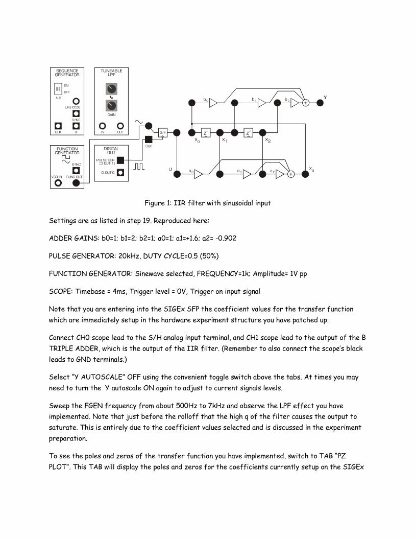
Figure 1: IIR filter with sinusoidal input
Settings are as listed in step 19. Reproduced here:
ADDER GAINS: b0=1; b1=2; b2=1; a0=1; a1=+1.6; a2= -0.902
PULSE GENERATOR: 20kHz, DUTY CYCLE=0.5 (50%)
FUNCTION GENERATOR: Sinewave selected, FREQUENCY=1k; Amplitude= 1V pp
SCOPE: Timebase = 4ms, Trigger level = 0V, Trigger on input signal
Note that you are entering into the SIGEx SFP the coefficient values for the transfer function
which are immediately setup in the hardware experiment structure you have patched up.
Connect CH0 scope lead to the S/H analog input terminal, and CH1 scope lead to the output of the B
TRIPLE ADDER, which is the output of the IIR filter. (Remember to also connect the scope’s black
leads to GND terminals.)
Select “Y AUTOSCALE” OFF using the convenient toggle switch above the tabs. At times you may
need to turn the Y autoscale ON again to adjust to current signals levels.
Sweep the FGEN frequency from about 500Hz to 7kHz and observe the LPF effect you have
implemented. Note that just before the rolloff that the high q of the filter causes the output to
saturate. This is entirely due to the coefficient values selected and is discussed in the experiment
preparation.
To see the poles and zeros of the transfer function you have implemented, switch to TAB “PZ
PLOT”. This TAB will display the poles and zeros for the coefficients currently setup on the SIGEx

SFP. You can see that the poles are very close to the unit circle (r=0.95), hence the high gain at the
peak before rolloff.
Figure 1: IIR filter with broad spectrum noise input
Viewing the system response using FFT
To view the response more dynamically, you will now change your input signal. Change the patching of
the FUNCTION GENERATOR to match Figure 2. You will now be inputting a flat noise spectrum and
viewing the FFT of the filtered output of the system.
Figure 2: IIR filter with flat broadband noise input

Ensure that SEQUENCE GENERATOR DIP switches are set to positions DOWN:DOWN. Set TLPF
knobs to fully clockwise for now. Switch to TAB “ZOOM FFT” to view time and frequency domains
simultaneously.
Change scope timebase to 100ms.
Setting up the input noise signal:
i) Reduce the TLPF GAIN by rotating counter clockwise until the output Ch1 signal (red) is no longer
saturated ie: less than 12V peak. A maximum level of 6 V is optimum to avoid saturation of internal
ADDER nodes.
ii) Reduce the noise bandwidth to around 4khz by rotating the TLPF block’s “Fc” control-counter
clockwise. View the noise spectrum as the white trace on the SCOPE & FFT windows.
The SFP should be similar to Figure 3 below:
Figure 3: IIR filter response using FFT; note the very small input signal (white)
At this point we can see and explore the issues relating to :
-controlling our input signal level and bandwidth
-viewing the response in both time and frequency domains

-setting up a transfer function with appropriate internal gains
We can also confirm that the peak of the response is correct according to the position of the poles.
ie: PZ PLOT tells us that poles are at 32 degrees, hence we expect a peak close to 32/360*20,000
= 1777 Hz. You can use the cursors in ZOOM FFT window to confirm this.
Dynamically varying the poles and zeros to adjust response using GAIN ADJUST manual control
Use the SIGEx board’s GAIN ADJUST knob to vary one of the coefficients by hand while viewing
the frequency response. Leave the default settings. Turn the knob until it reads +1.6 (located in the
COEFFICIENT SELECTOR window), then select radio button “ a1 ”. View the frequency response
while slowly varying the value of a1. You will find that the peak frequency changes.
Find a range of a1 settings that work well and then view PZ PLOT while varying across that range.
You will see the poles moving and reflecting the changing a1 coefficient. (Theory states that a1=-2σ,
which is the real part of the pole and its conjugate.) You can confirm this relationship from values
displayed on PZ PLOT.
Set a1 back to +1.6, select OFF, then set GAIN ADJUST to -0.9, and select a2 radio button.
Varying a2 will vary the gain or peak level of the filter. Notice what happens in the time domain
when a2 = -1.0. The filter breaks into oscillation. View the poles again using PZ PLOT while varying a2.
(Theory states that a2 = r2).
Set a2 back to -0.9, then select OFF again at the COEFFICIENT SELECTOR to disable the GAIN
ADJUST control.
Using Digital Filter Design toolkit to implement Highpass filters
Switch to the DFD TAB. This will automatically load the computed coefficients for the selected
filter onto the SIGEx board. You can see the values on the TAB setup in the GAIN input controls on
the SIGEx SFP.
Connect CH0 to “ x0 ”, and CH1 to “Y” and view the internal signal levels at “x0” by switching to the
ZOOM FFT tab. Set the TLPF GAIN higher but avoid saturating.These filters have lower internal
gains than the previous ones. Vary the filter design type (at the DFD tab by clicking on “DESIGN
METHOD” to select) and view the output responses using ZOOM FFT.
Set timebase to 100ms.
Again you can use the cursors to compare the actual performance to theory and design.
You can expect to see a display like so:

Figure 4: Highpass filter response using FFT; x0 (white); Y (red)

Figure 5: DFD tab used to design filters and setup coefficients to the patched SIGEx board
Default values are chosen to enable students to see textbook like responses which they can easily
measure.
Conclusion
This quickstart guide is designed to demonstrate quickly, and without supporting preparation, some
of the powerful interactivity of the SIGEx board. Students can expect to gradually build up to this
level of complexity with the many documented earlier experiments from the SIGEx Lab Manual.
By building and controlling experiments using real circuits, students will develop confidence and
intuitive familiarity with the theory they have covered in class.

References
Lathi.B.P. , “Signal processing & Linear Systems”, Oxford University Press
Oppenheim.A.V.,Wilsky.A.S., “Signals & Systems”, Prentice Hall, 2nd edition
Haykin, Van Veen, “Signals and Systems”, Wiley, 2nd edition
Ziemer.R.E,Tranter.W.H, Fannin.D.R, “Signals & Systems: Continuous and Discrete”, Prentice Hall, 4th edition
Boulet.B.: “Fundamentals of Signals & Systems”, Thomson/Delmar Learning
Frederick.D.K.,Carlson.A.B.: “Linear systems in communication and control”,
Wiley
Carlson.A.B.: “Communication systems”, McGraw Hill, 2nd edition
Smith.C.E.: “Applied mathematics for radio and communication engineers”,
Dover
Lynn.P.A., “An introduction to the analysis and processing of signals”, Macmillan
Maor.E.,”e: The story of a number”, Princeton University Press
Radzyner.R / Rakus.M: “Signals and systems experiments with Emona TIMS”, Emona Instruments, Issue 3.0
Langton, C.: “Fourier analysis made easy”, www.complextoreal.com
McClellan.J.H, Schafer.R.W, Yoder.M.A, “DSP First”, Prentice Hall


Emona SIGEx™ Lab Manual -
Signals & Systems Experiments with the Emona SIGEx
Volume 1
Emona Instruments Pty Ltd
78 Parramatta Road web: www.emona-tims.com
Camperdown NSW 2050 telephone: +61-2-9519-3933
AUSTRALIA fax: +61-2-9550-1378
The "SIGEx" logo is a trademark of Emona TIMS PTY LTD