silicon carbide gto thyristor for hvdc...
TRANSCRIPT

Silicon Carbide GTO ThyristorLoss Model for
HVDC Application

Why SiC?
• Low resistance – reduced drift region widths due to high band gap ⇒ hence less on state resistance
• High switching frequency – the high velocity saturation and thinner drift region ⇒ the device switches faster.
• Smaller heat sinks – thermal conductivity of silicon carbide is three times greater than silicon and hence better heat dissipation. This results in reduced thermal management system.
• High radiation tolerance and minimal shielding – the electrical characteristics of silicon carbide device do not vary with temperature.
Why SiC?
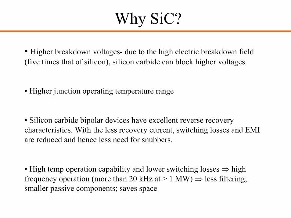
• Higher breakdown voltages- due to the high electric breakdown field (five times that of silicon), silicon carbide can block higher voltages.
• Higher junction operating temperature range
• Silicon carbide bipolar devices have excellent reverse recoverycharacteristics. With the less recovery current, switching losses and EMI are reduced and hence less need for snubbers.
• High temp operation capability and lower switching losses ⇒ high frequency operation (more than 20 kHz at > 1 MW) ⇒ less filtering; smaller passive components; saves space

• Material availability and quality issues -micropipes
• SiC technology-polytype crystal growth(6H,4H-SiC)-SiC-SiO2 interface - ion implantation
• Cost of the material.
• Also, the increase in rating of auxiliary components and effective packaging techniques are important
How far is SiC from commercialization?
Micropipe defect
OutlineSiC MATERIAL
SiC GTO Thyristor
HVDC System
Results
Conclusion
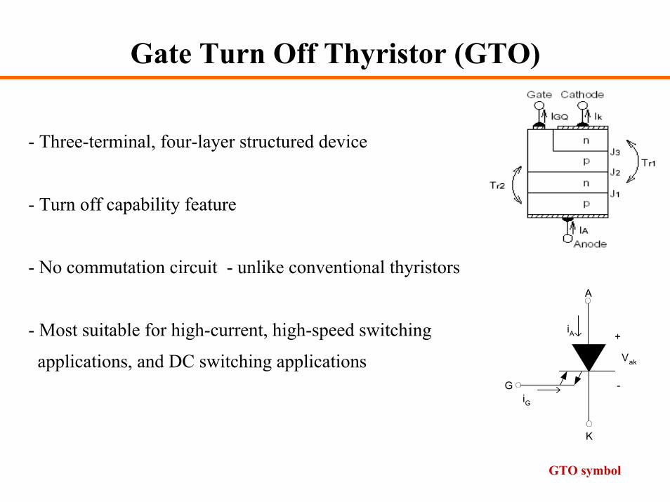
Gate Turn Off Thyristor (GTO)
- Three-terminal, four-layer structured device
- Turn off capability feature
- No commutation circuit - unlike conventional thyristors
- Most suitable for high-current, high-speed switching
applications, and DC switching applications +
-
Vak
iG
K
iA
A
G
GTO symbol
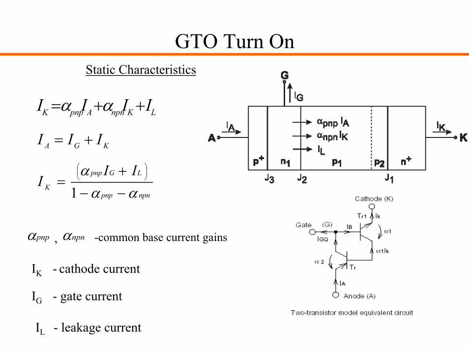
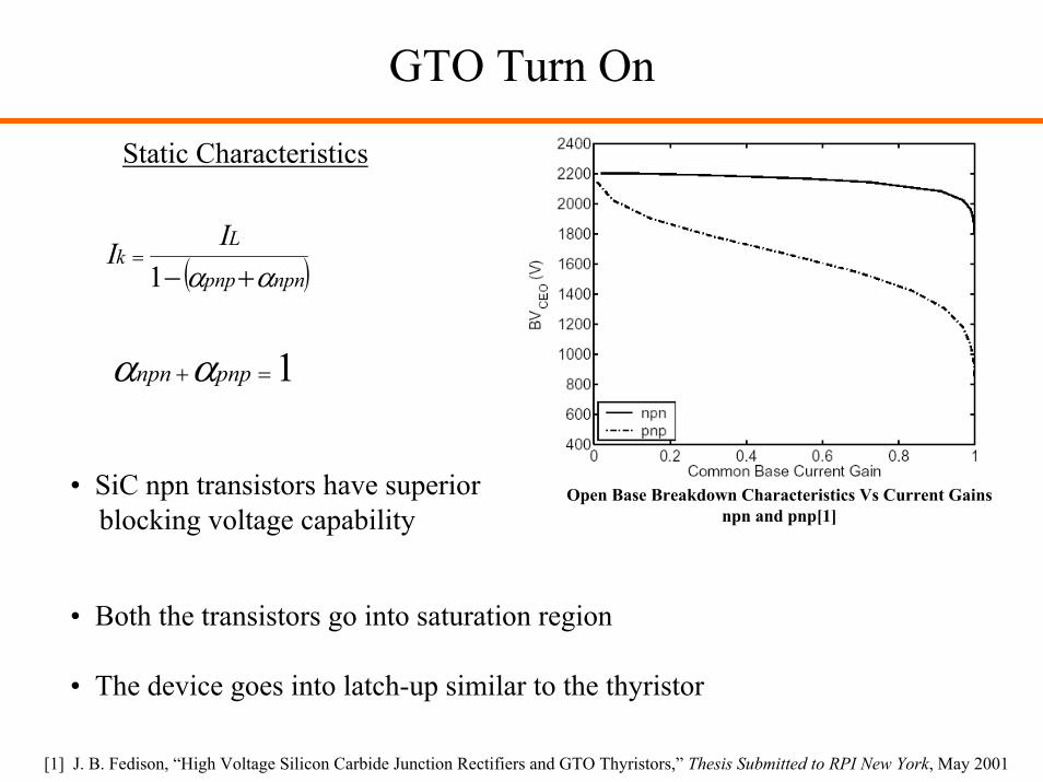
GTO Turn OnStatic Characteristics
LKnpnApnpK IIII ++= αα
KGA III +=
npnpnp
LGpnp
K
III
ααα
−−+
=
1
IK - cathode current
IG - gate current
IL - leakage current
-common base current gainspnpα npnα,
GTO Turn On
Open Base Breakdown Characteristics Vs Current Gains npn and pnp[1]
Static Characteristics
( )npnpnp
Lk
IIαα +−
=1
1=+ pnpnpn αα
• SiC npn transistors have superiorblocking voltage capability
• Both the transistors go into saturation region
• The device goes into latch-up similar to the thyristor
[1] J. B. Fedison, “High Voltage Silicon Carbide Junction Rectifiers and GTO Thyristors,” Thesis Submitted to RPI New York, May 2001
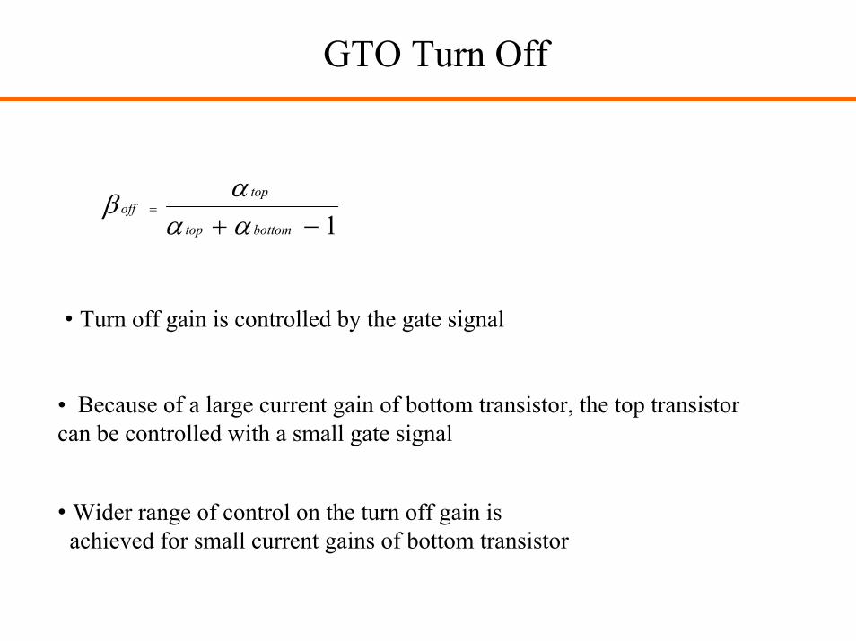
GTO Turn Off
1−+=
bottomtop
topoff
αααβ
• Turn off gain is controlled by the gate signal
• Because of a large current gain of bottom transistor, the top transistor can be controlled with a small gate signal
• Wider range of control on the turn off gain isachieved for small current gains of bottom transistor

Structure
• Asymmetrical, complementary structure
• Partial ionization of p-type impurities – low conduction capability
• Reduced drift layer thickness compared to silicon
• P+ buffer layer –increase the turn off gain by decreasingthe injection efficiency of npn transistor
A K
G
J1J2J3
P+ n1 n+P1
anode n-base drift layer cathode
Complementary asymmetric SiC GTO thyristor structure
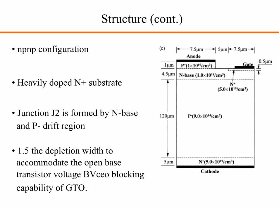
Structure (cont.)
• npnp configuration
• Heavily doped N+ substrate
• Junction J2 is formed by N-base and P- drift region
• 1.5 the depletion width to accommodate the open base transistor voltage BVceo blocking capability of GTO.

Loss Model Equations
Conduction losses
)2/3exp()/()8/3()/( caBgstateon ELVqkTJqEJP ⋅⋅⋅+⋅=− π
)2()( 2dacdaB NNqENNV ⋅⋅⋅+= ε
pna τττ +=
5.0)( aaa DL τ⋅=
)(2 pnpna DDDDD +⋅⋅=
( ) nn qkTD µ⋅=
Then final expression for conduction losses can be given as,
)/()()/(2/()5.1)((
)exp()./).(8/3()/(
pnapndabdda
gstateon
qKTNNqENND
DqkTJqEJP
µµτµµε
π
+⋅⋅⋅⋅⋅⋅⋅⋅=
⋅+⋅=
+
−
( ) pp qkTD µ⋅=
This equation is dependent on doping densities, mobilities, temperature,applied voltage, and current.

Loss Model
• Si GTO thyristor losses are more ⇒ difference in the on-state specific resistance.
• Electric field for Si is lower ⇒hence specific resistance is more
• For a given operating current, conduction losses vary with thesecond term in the equation,which is a function of the on-state specific resistance
300 350 400 450 500 550 6000
100
200
300
400
500
600
700
Temperature(k)
Pow
er (w
)
Conduction Losses
S i
S iC
3
4 2
cnssp
E
BVRµε
=
Conduction losses for V= 5000 V and J=100 A/cm2
)2/3exp()/()8/3()/( caBgstateon ELVqkTJqEJP ⋅⋅⋅+⋅=− π
Loss Model
Switching losses
τJαV/V)αV/(E(ε/E anpn,Bnpncsoff ⋅+−⋅⋅= max121
agcnsBaBcson Jτq)/(E)Eµ)/(εVτ(JV/VVEε/E ⋅+⋅+⋅⋅= ⋅⋅⋅ 2331 322
The switching power losses can be calculated using the total energy loss equation as,
soffonswitching fEEP ⋅+= )(
Loss Model
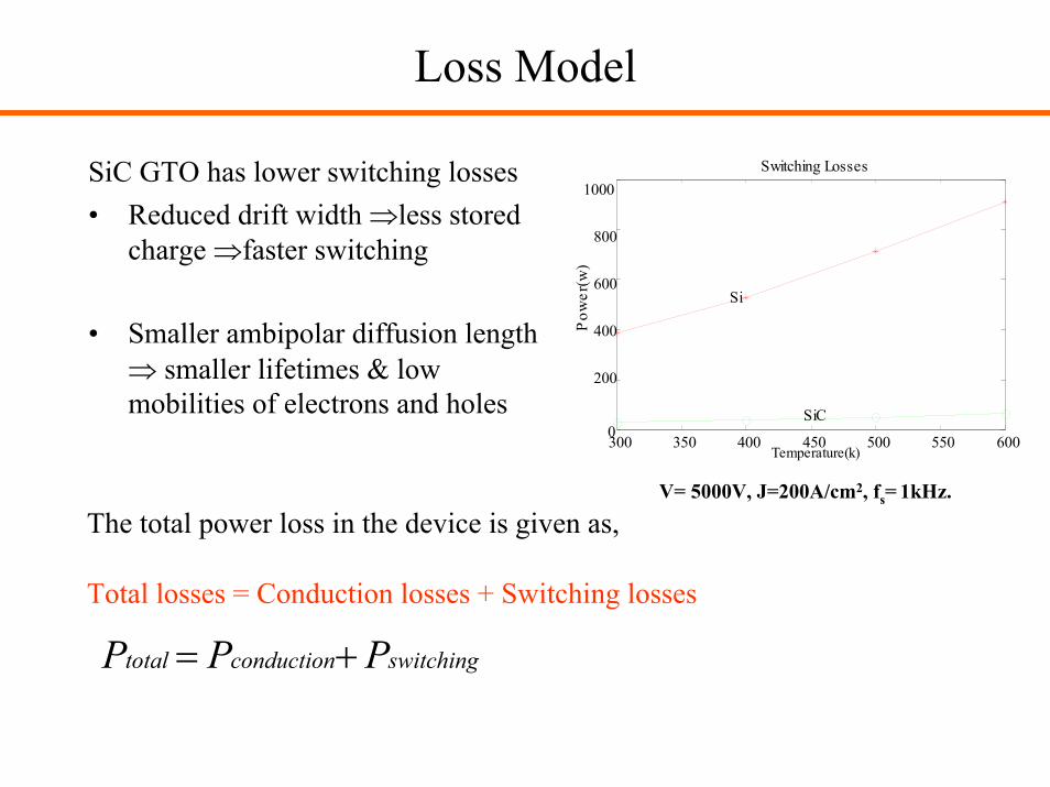
SiC GTO has lower switching losses• Reduced drift width ⇒less stored
charge ⇒faster switching
• Smaller ambipolar diffusion length ⇒ smaller lifetimes & low mobilities of electrons and holes
300 350 400 450 500 550 6000
200
400
600
800
1000
Temperature(k)
Pow
er(w
)
Switching Losses
Si
SiC
The total power loss in the device is given as,
Total losses = Conduction losses + Switching losses
V= 5000V, J=200A/cm2, fs= 1kHz.
switchingconductiontotal PPP +=
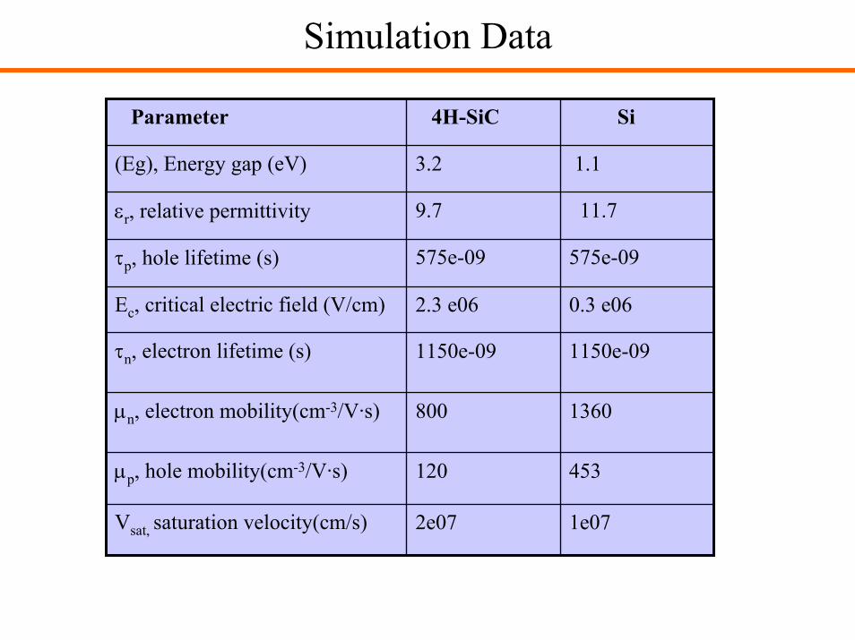
Simulation Data
453120µp, hole mobility(cm-3/V·s)
1150e-091150e-09τn, electron lifetime (s)
1e072e07Vsat, saturation velocity(cm/s)
1360800µn, electron mobility(cm-3/V·s)
0.3 e062.3 e06Ec, critical electric field (V/cm)
575e-09575e-09τp, hole lifetime (s)
11.79.7εr, relative permittivity
1.1 3.2 (Eg), Energy gap (eV)
Si4H-SiCParameter
Simulations
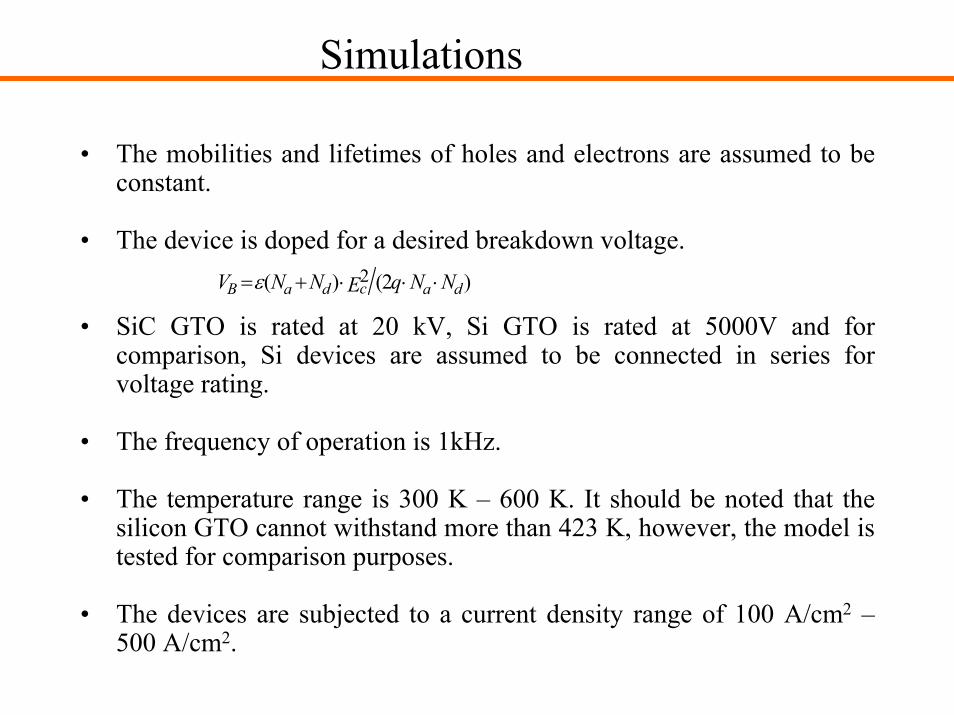
• The mobilities and lifetimes of holes and electrons are assumed to be constant.
• The device is doped for a desired breakdown voltage.
• SiC GTO is rated at 20 kV, Si GTO is rated at 5000V and for comparison, Si devices are assumed to be connected in series forvoltage rating.
• The frequency of operation is 1kHz.
• The temperature range is 300 K – 600 K. It should be noted that the silicon GTO cannot withstand more than 423 K, however, the model is tested for comparison purposes.
• The devices are subjected to a current density range of 100 A/cm2 –500 A/cm2.
)2()( 2dacdaB NNqENNV ⋅⋅⋅+=ε
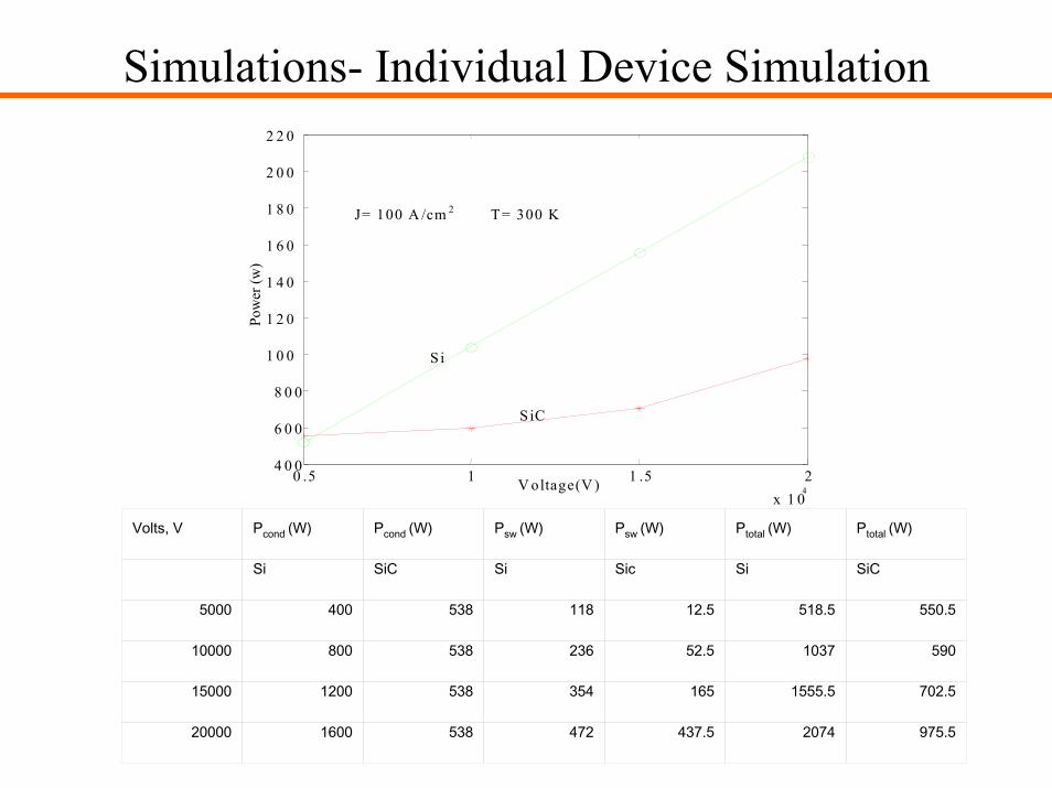
Simulations- Individual Device Simulation
Volts, V Pcond (W) Pcond (W) Psw (W) Psw (W) Ptotal (W) Ptotal (W)
Si SiC Si Sic Si SiC
5000 400 538 118 12.5 518.5 550.5
10000 800 538 236 52.5 1037 590
15000 1200 538 354 165 1555.5 702.5
20000 1600 538 472 437.5 2074 975.5
0 .5 1 1 .5 2x 1 0
4
4 0 0
6 0 0
8 0 0
1 0 0
1 2 0
1 4 0
1 6 0
1 8 0
2 0 0
2 2 0
Pow
er (w
)
V oltage(V )
S i
S iC
J= 100 A /cm 2 T= 300 K
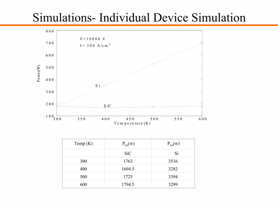
Simulations- Individual Device Simulation
3 0 0 3 5 0 4 0 0 4 5 0 5 0 0 5 5 0 6 0 01 0 0
2 0 0
3 0 0
4 0 0
5 0 0
6 0 0
7 0 0
8 0 0
T e m p e ra tu re (K )
Pow
er(W
) V = 1 0 0 0 0 V J = 3 0 0 A /c m 2
S i
S iC
Temp (K) Ptot(w) Ptot(w)
SiC Si
300 1762 3516
400 1694.5 3282
500 1725 3394
600 1794.5 3299
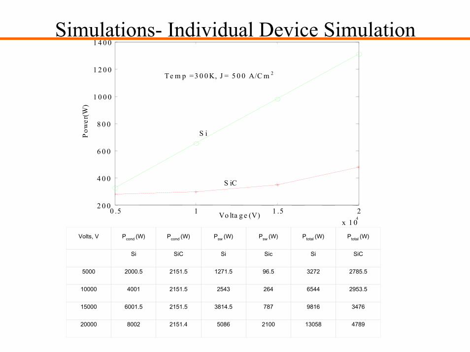
0 .5 1 1 .5 2x 1 0
4
2 0 0
4 0 0
6 0 0
8 0 0
1 0 0 0
1 2 0 0
1 4 0 0
Vo lta g e (V)
Pow
er(W
)
S i
S iC
Te m p =3 0 0 K, J = 5 0 0 A/C m 2
Volts, V Pcond (W) Pcond (W) Psw (W) Psw (W) Ptotal (W) Ptotal (W)
Si SiC Si Sic Si SiC
5000 2000.5 2151.5 1271.5 96.5 3272 2785.5
10000 4001 2151.5 2543 264 6544 2953.5
15000 6001.5 2151.5 3814.5 787 9816 3476
20000 8002 2151.4 5086 2100 13058 4789
Simulations- Individual Device Simulation
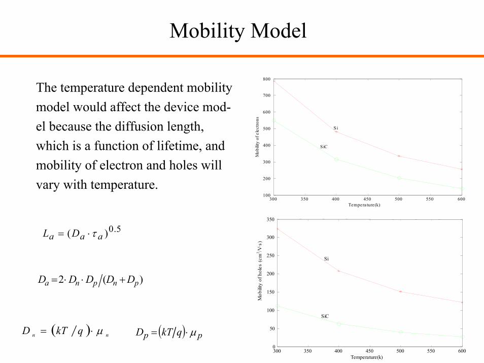
Mobility Model
The temperature dependent mobility model would affect the device mod-el because the diffusion length, which is a function of lifetime, and mobility of electron and holes will vary with temperature.
300 350 400 450 500 550 6000
50
100
150
200
250
300
350
Temperature(k)
Mob
ility
of h
oles
(cm
2 /V·s
)
SiC
Si
5.0)( aaa DL τ⋅=
)(2 pnpna DDDDD +⋅⋅=
( ) nn qkTD µ⋅= ( ) pp qkTD µ⋅=
300 350 400 450 500 550 600100
200
300
400
500
600
700
800
Tempera ture(k)
Mob
ility
of e
lect
rons
S iC
S i

Mobility
• Mobility is defined as the average velocity of free carriers in a semiconductor due to an applied electric field.
• Mobility affects the flow of electrons and hence current.
• Scattering of electrons causes reduction in mobility- bulk mobility is calculated neglecting the
scattering at surface and has higher value
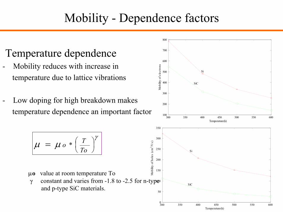
Mobility - Dependence factors
Temperature dependence- Mobility reduces with increase in
temperature due to lattice vibrations
- Low doping for high breakdown makes temperature dependence an important factor
γµµ
=
ToTo *
µo value at room temperature Toγ constant and varies from -1.8 to -2.5 for n-type
and p-type SiC materials.
300 350 400 450 500 550 600100
200
300
400
500
600
700
800
Temperature(k)
Mob
ility
of e
lect
rons
SiC
Si
300 350 400 450 500 550 6000
50
100
150
200
250
300
350
Temperature(k)
Mob
ility
of h
oles
(cm
2 /V·s
)
SiC
Si
Mobility - Dependence factors
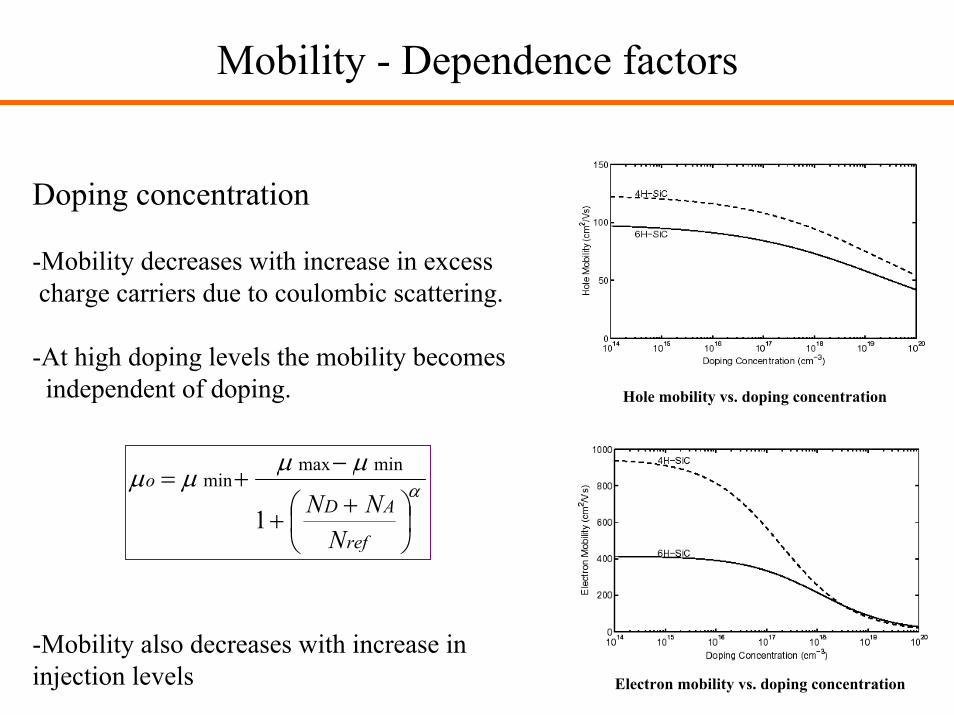
Doping concentration
-Mobility decreases with increase in excesscharge carriers due to coulombic scattering.
-At high doping levels the mobility becomes independent of doping.
-Mobility also decreases with increase in injection levels Electron mobility vs. doping concentration
Hole mobility vs. doping concentration
αµµµµ
++
−+=
ref
ADo
NNN1
minmaxmin
Mobility - Dependence factors
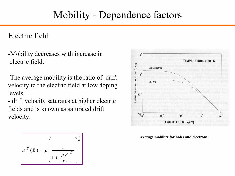
Electric field
-Mobility decreases with increase in electric field.
-The average mobility is the ratio of drift velocity to the electric field at low doping levels.- drift velocity saturates at higher electric fields and is known as saturated drift velocity.
β
βµµµ
1
1
1)(
+
=
s
E
vE
E
Average mobility for holes and electrons
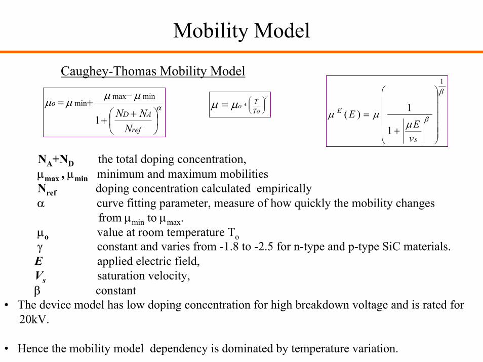
Mobility Model
Caughey-Thomas Mobility Modelβ
βµµµ
1
1
1)(
+
=
s
E
vE
Eα
µµµµ
+
+
−+=
ref
ADo
NNN1
minmaxmin
γ
µµ
=ToTo *
NA+ND the total doping concentration, µmax , µmin minimum and maximum mobilitiesNref doping concentration calculated empiricallyα curve fitting parameter, measure of how quickly the mobility changes
from µmin to µmax. µo value at room temperature Toγ constant and varies from -1.8 to -2.5 for n-type and p-type SiC materials.E applied electric field,Vs saturation velocity, β constant
• The device model has low doping concentration for high breakdown voltage and is rated for 20kV.
• Hence the mobility model dependency is dominated by temperature variation.

Mobility Model Data
Si 4H-SiC
Minimum electron mobility, µminn [cm2/V·s] 65 50
Maximum electron mobility, µmaxn [cm2/V·s] 1360 950
Minimum hole mobility, µminp [cm2/V·s] 50 10
Maximum hole mobility, µmaxp [cm2/V·s] 505 180
Electron ionization coefficient, αn 0.91 0.76
Hole ionization coefficient, αp 0.63 0.56
Reference electron concentration, Nrefn [cm-3] 8.5e16 2.2e17
Reference hole concentration, Nrefp [cm-3] 6.3e16 2.35e17
Lifetime
• Lifetime is measure of duration of a charge carrier before it recombines for equilibrium conditions.
• Recombination can occur in several ways when electrons drop from valence band to conduction band :- surface trap recombination- recombination center
• There are several different recombination processes:- Shockley-Read-Hall recombination- Auger recombination
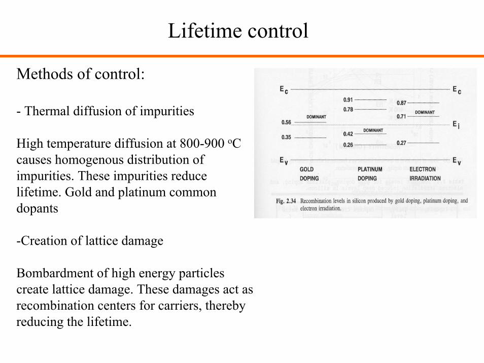
Lifetime control
Methods of control:
- Thermal diffusion of impurities
High temperature diffusion at 800-900 oCcauses homogenous distribution of impurities. These impurities reduce lifetime. Gold and platinum common dopants
-Creation of lattice damage
Bombardment of high energy particles create lattice damage. These damages act as recombination centers for carriers, thereby reducing the lifetime.
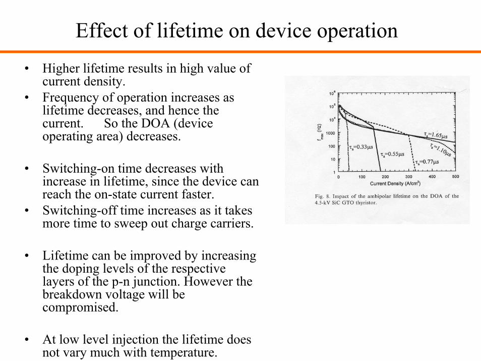
Effect of lifetime on device operation• Higher lifetime results in high value of
current density.• Frequency of operation increases as
lifetime decreases, and hence the current. So the DOA (device operating area) decreases.
• Switching-on time decreases with increase in lifetime, since the device can reach the on-state current faster.
• Switching-off time increases as it takes more time to sweep out charge carriers.
• Lifetime can be improved by increasing the doping levels of the respective layers of the p-n junction. However the breakdown voltage will be compromised.
• At low level injection the lifetime does not vary much with temperature.
Diffusion Length
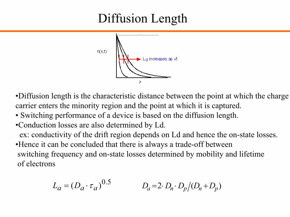
•Diffusion length is the characteristic distance between the point at which the charge carrier enters the minority region and the point at which it is captured.• Switching performance of a device is based on the diffusion length.•Conduction losses are also determined by Ld.ex: conductivity of the drift region depends on Ld and hence the on-state losses.
•Hence it can be concluded that there is always a trade-off between switching frequency and on-state losses determined by mobility and lifetimeof electrons
5.0)( aaa DL τ⋅= )(2 pnpna DDDDD +⋅⋅=

Simulations: Device simulation for J = 200 A/cm2, V = 5000V
T (K) Pcond (W) Pcond (W) Psw (W) Psw (W) Ptotal (W) Ptotal (W)
Si SiC Si Sic Si SiC
300 2491.5 1375.5 383.5 29.5 2875 2785.5
400 5194.4 2476.5 527.5 37.5 5722 2953.5
500 9093.5 4704 713.5 48 9807 3476
600 1.381e 9184 910 63 1.409e 4789
T (K) Pcond (W) Pcond (W) Psw (W) Psw (W) Ptotal (W) Ptotal (W)
Si SiC Si Sic Si SiC
300 2491.5 1375.5 383.5 29.5 2875 2785.5
400 5194.4 2476.5 527.5 37.5 5722 2953.5
500 9093.5 4704 713.5 48 9807 3476
600 1.381e 9184 910 63 1.409e 4789

T (K) Pcond (W) Pcond (W) Psw (W) Psw (W) Ptotal (W) Ptotal (W)
Si SiC Si Sic Si SiC
300 9966 3193 2792 172 1.27E+04 3366
400 2.08E+04 5699 4020 188.5 2.48E+04 5856.5
500 3.37E+04 1.02E+04 5550 221.5 4.19E+04 1.05E+04
600 5.24E+04 1.88E+04 7137 265.5 5.98E+04 1.91E+04
T (K) Pcond (W) Pcond (W) Psw (W) Psw (W) Ptotal (W) Ptotal (W)
Si SiC Si Sic Si SiC
300 9966 3193 2792 172 1.27E+04 3366
400 2.08E+04 5699 4020 188.5 2.48E+04 5856.5
500 3.37E+04 1.02E+04 5550 221.5 4.19E+04 1.05E+04
600 5.24E+04 1.88E+04 7137 265.5 5.98E+04 1.91E+04
Simulations: Device simulation for J = 400 A/cm2, V = 10000V
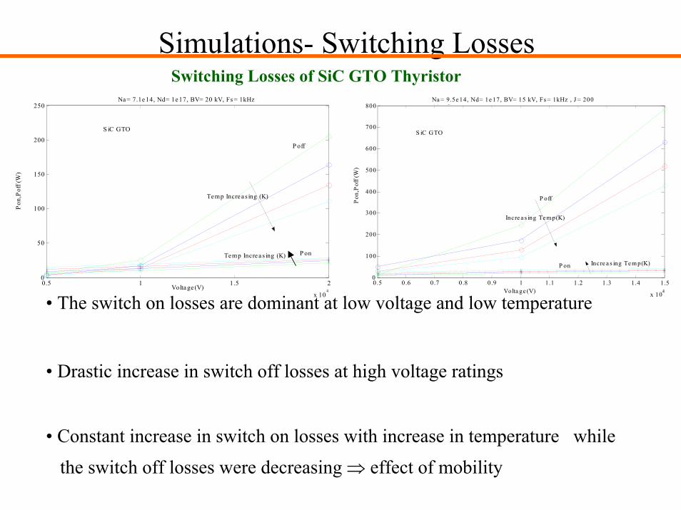
Simulations- Switching LossesSwitching Losses of SiC GTO Thyristor
0.5 1 1.5 2
x 104
0
50
100
150
200
250
Volta ge (V)
Pon
,Pof
f (W
)
Na = 7.1e 14, Nd= 1e 17, BV= 20 kV, Fs = 1kHz
P on
P off
Temp Incre a s ing (K)
Temp Incre a s ing (K)
S iC GTO
0.5 0.6 0.7 0.8 0.9 1 1.1 1.2 1.30
100
200
300
400
500
600
700
800
Volta ge (V)
Pon
,Pof
f (W
)
Na = 9.5e 14, Nd= 1e 17, BV= 15 kV, Fs = 1kHz , J = 200 A/ 2
Incre a s ing Te m p(K)
P on
P off
Incre a s ing T
• The switch on losses are dominant at low voltage and low temperature
• Drastic increase in switch off losses at high voltage ratings
• Constant increase in switch on losses with increase in temperature while
the switch off losses were decreasing ⇒ effect of mobility
1.4 1.5 x 10⁴
e m p(K)
S iC GTO
• Conduction losses dominate because, at lower switching frequency the switching losses are low, and the main power loss is a function of on-state resistance.
• It is found that the conduction losses of silicon GTO thyristor are at least twice more than silicon carbide device.
• The switching losses of silicon carbide GTO thyristor are at least 12 times less than the silicon device.
• The device operating area (DOA) limits can be improved due to reduced losses ⇒ the maximum frequency can be increased for a given current density and operating voltage
• This difference in losses shows that SiC devices have high efficiency compared to silicon.
• The number of SiC devices per converter leg required is less, due to the higher voltage rating of the device.
Inference
Outline
SiC MATERIAL
SiC GTO Thyristor
HVDC SystemResults
Conclusion

HVDC System
• The configuration chosen for the study is a monopolar configuration.
• The transmission system is basedon voltage source converter technology. Converter at both the ends is a voltage source converter also known as forced commutated converter.
• The system model is designed to emulate the ac characteristics.
Rg1
Rg2
Rg3
Rg4
Rg5
Rg6
1 3 5
4 6 2
A
B
C
A
B
C 62.5
#2 #1
13.8
100.0 [MVA] 500.0
dcVltg

HVDC System -VSC Technology
VSC 2
dc line
C 1 C 2
AC AC
Y- - YVSC 1
Basic configuration of VSC transmission
VvscVac
XI
(Vvsc - Vac)
Phasor diagram Equivalent circuit of VSC transmission
( ) XVVVQ vscacvsc ⋅−⋅= δcosXVVP acvsc δsin⋅⋅=

HVDC System
Control system
The active power transfer in a system is given as,
V1, V2 - ac voltage magnitudes at the sending endand receiving end respectively.
X - inductive reactance of the dc cableδ - angle between the sending and receiving end voltages.
XVVP δsin21 ⋅⋅=

HVDC SystemOverview of the Control System
VSC 1 VSC 2
AC ACAC Filter
Transformer Y-
Systemimpedance
dc line
Sending end (Rectifier)Receiving end (Inverter)
PPWM
Power Controller
Reactivepower
controller
Receiving endVoltage
controllerPWM
dc Voltagecontroller
Qref
Qmeas
shft
mr
Pdc(ref)dcvltgi
RePh
SePh
dc set voltage
Vac
Vrefshfti
mi
XVVP rsrs )sin( δδ −⋅⋅=

HVDC System
System Simulations• The system model and the various control systems were
implemented using PSCAD/EMTDC software.
• PSCAD/EMTDC is a simulation tool for analyzing power systems. PSCAD is the graphical user interface and EMTDC is the simulation engine.
• The software also has an excellent feature of interfacing MATLAB/SIMULINK.
• The system model has been developed from an example of the PSCAD and modified for the specifications.
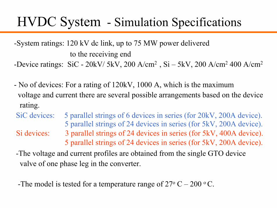
HVDC System - Simulation Specifications-System ratings: 120 kV dc link, up to 75 MW power delivered
to the receiving end-Device ratings: SiC - 20kV/ 5kV, 200 A/cm2 , Si – 5kV, 200 A/cm2 400 A/cm2
- No of devices: For a rating of 120kV, 1000 A, which is the maximum voltage and current there are several possible arrangements based on the device rating.
SiC devices: 5 parallel strings of 6 devices in series (for 20kV, 200A device).5 parallel strings of 24 devices in series (for 5kV, 200A device).
Si devices: 3 parallel strings of 24 devices in series (for 5kV, 400A device).5 parallel strings of 24 devices in series (for 5kV, 200A device).
-The voltage and current profiles are obtained from the single GTO device valve of one phase leg in the converter.
-The model is tested for a temperature range of 27o C – 200 o C.
Outline
SiC MATERIAL
SiC GTO Thyristor
HVDC System
ResultsConclusion
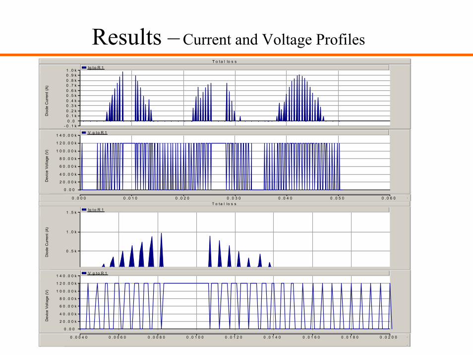
Results – Current and Voltage ProfilesT o t a l lo s s
0 . 0 0 0 0 . 0 1 0 0 . 0 2 0 0 . 0 3 0 0 . 0 4 0 0 . 0 5 0 0 . 0 6 0 ...
- 0 . 1 k0 . 0
0 . 1 k0 . 2 k0 . 3 k0 . 4 k0 . 5 k0 . 6 k0 . 7 k0 . 8 k0 . 9 k1 . 0 k
Dio
de C
urre
nt (A
)
Ig t o R 1
0 . 0 0
2 0 . 0 0 k
4 0 . 0 0 k
6 0 . 0 0 k
8 0 . 0 0 k
1 0 0 . 0 0 k
1 2 0 . 0 0 k
1 4 0 . 0 0 k
Dev
ice
Volta
ge (V
)
V g t o R 1
T o t a l lo s s
0 . 0 0 4 0 0 . 0 0 6 0 0 . 0 0 8 0 0 . 0 1 0 0 0 . 0 1 2 0 0 . 0 1 4 0 0 . 0 1 6 0 0 . 0 1 8 0 0 . 0 2 0 0 ...
0 . 5 k
1 . 0 k
1 . 5 k
Dio
de C
urre
nt (A
)
Ig t o R 1
0 . 0 0
2 0 . 0 0 k
4 0 . 0 0 k
6 0 . 0 0 k
8 0 . 0 0 k
1 0 0 . 0 0 k
1 2 0 . 0 0 k
1 4 0 . 0 0 k
Dev
ice
Volta
ge (V
)
V g t o R 1

Results – Power Loss Profiles
Loss Profile for SiC GTO (423 K)
T o ta l lo s s
0 .0 0 0 0 .0 1 0 0 .0 2 0 0 .0 3 0 0 .0 4 0 0 .0 5 0 ...
0 .0
5 .0 k
1 0 .0 k
1 5 .0 k
2 0 .0 k
2 5 .0 k
3 0 .0 k
3 5 .0 k
Pow
er D
ensi
ty (W
/Sq.
cm)
Ig t o R 1 T o ta l lo s s
0 .0 0
2 0 .0 0 k
4 0 .0 0 k
6 0 .0 0 k
8 0 .0 0 k
1 0 0 .0 0 k
1 2 0 .0 0 k
1 4 0 .0 0 k
Dev
ice
Volta
ge (V
)
V g to R 1
T o ta l lo s s
0 .0 0 0 0 .0 1 0 0 .0 2 0 0 .0 3 0 0 .0 4 0 0 .0 5 0 ...
- 2 0 .0 0 k
- 1 0 .0 0 k
0 .0 0
1 0 .0 0 k
2 0 .0 0 k
3 0 .0 0 k
4 0 .0 0 k
5 0 .0 0 k
Pow
er D
ensi
ty (W
/Sq.
cm)
T o ta l lo s s
0 .0 0
2 0 .0 0 k
4 0 .0 0 k
6 0 .0 0 k
8 0 .0 0 k
1 0 0 .0 0 k
1 2 0 .0 0 k
1 4 0 .0 0 k
Dev
ice
Volta
ge (V
)
V g to R 1
SiC GTO Power Loss
Si GTO Power Loss
Loss Profile for Si GTO (423 K)

GTO Efficiency Calculation
• The GTO efficiency is calculated based on the power loss profile obtained for different operating conditions.
• It is the instantaneous loss as a function of the instantaneous current, which depends on the modulation index and the switching angles generated by the PWM.
• The average loss over few cycles of the fundamental is calculated to find the cyclic power loss (average power loss for each cycle of the output voltage).
• The maximum and minimum power loss for a single device, over a few cycles is measured from the plots, and the corresponding converter controlled switches efficiency is calculated.

Cyclic Power Loss Plots
0 2 4 6 8 10250
300
350
400
450
Pow
er lo
ss (W
/Sq.
cm)
T=300K
0 2 4 6 8 10800
900
1000
1100
1200
1300
1400
1500
Pow
er lo
ss (W
/Sq.
cm) T=373K
0 2 4 6 8 101800
2000
2200
2400
2600
2800
3000
3200
Pow
er lo
ss (W
.Sq.
cm)
T=423K
0 2 4 6 8 103500
4000
4500
5000
5500
6000
6500
Pow
er lo
ss (W
/Sq.
cm)
T=473K
0 2 4 6 8 10250
300
350
400
450
500
Pow
er lo
ss (W
/Sq.
cm)
T=300K
0 2 4 6 8 10700
800
900
1000
1100
1200
1300
Pow
er lo
ss (W
/Sq.
cm) T=373K
0 2 4 6 8 101400
1600
1800
2000
2200
2400
2600
Pow
er lo
ss(W
/Sq.
cm)
T=423K
0 2 4 6 8 102500
3000
3500
4000
4500
5000
Pow
er lo
ss(W
/Sq.
cm)
T=473K
Cyclic Power Loss Plots for Si 5kV, 200 A/cm2GTO Cyclic Power Loss Plots for SiC 20 kV, 200 A/cm2 GTO

GTO Efficiency Calculation
• Minimum efficiency = (dc power – Ploss(max))/dc power
Ploss(max) = Pmax •(No. of devices in the converter)
• Maximum efficiency = (dc power- Ploss(min))/dc power
Ploss(min)= Pmin •(No. of devices in the converter)
• No. of devices = (No. of devices for voltage sharing)•(No. of devices for current dividing)•6.

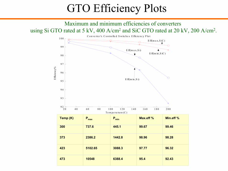
GTO Efficiency PlotsMaximum and minimum efficiencies of converters
using Si GTO rated at 5 kV, 200 A/cm2 and SiC GTO rated at 20 kV, 200 A/cm2.
2 0 4 0 6 0 8 0 1 0 0 1 2 0 1 4 0 1 6 0 1 8 0 2 0 09 2
9 3
9 4
9 5
9 6
9 7
9 8
9 9
1 0 0
T em p era tu re (C )
Effic
ienc
y%
C o n v erte r’s C o n tro lled S w itch es E ffic ien c y P lo t
E ff(m ax ,S iC
E ff(m in ,S iC
E ff(m ax ,S i
E ff(m in ,S i)
Efficiency of Si GTO Converter’s Controlled Switches Efficiency of SiC GTO Converter’s Controlled Switches
Temp (K) Pmax Pmin Max.eff % Min.eff %
300 433.3 262.7 99.68 99.48
373 1443.1 873.7 98.75 98.26
423 3041.2 1842.4 97.78 96.35
473 6301.9 3818.9 95.41 92.43
Temp (K) Pmax Pmin Max.eff % Min.eff %
300 433.3 262.7 99.68 99.48
373 1443.1 873.7 98.75 98.26
423 3041.2 1842.4 97.78 96.35
473 6301.9 3818.9 95.41 92.43
Temp (K) Pmax Pmin Max.eff % Min.eff %
300 475.2 300.6 99.9 99.85
373 1245.6 771.8 99.76 99.62
423 2402.1 1472.8 99.55 99.77
473 4506.9 2749.3 99.17 98.64
Temp (K) Pmax Pmin Max.eff % Min.eff %
300 475.2 300.6 99.9 99.85
373 1245.6 771.8 99.76 99.62
423 2402.1 1472.8 99.55 99.77
473 4506.9 2749.3 99.17 98.64
GTO Efficiency Plots
2 0 4 0 6 0 8 0 1 0 0 1 2 0 1 4 0 1 6 0 1 8 0 2 0 09 2
9 3
9 4
9 5
9 6
9 7
9 8
9 9
Te m p e ra tu re (C )
Effi
cien
cy%
C o n ve rte r’s C o n tro lle d S witc h e s E ffic ie n c y P lo t
E ff(m a x,S i) E ff(m in ,S iC )
E ff(m in ,S i)
E ff(m a x,S iC )
Temp (K) Pmax Pmin Max.eff % Min.eff %
300 737.6 445.1 99.67 99.46
373 2386.2 1442.8 98.96 98.28
423 5102.65 3088.3 97.77 96.32
473 10548 6388.4 95.4 92.43
Temp (K) Pmax Pmin Max.eff % Min.eff %
300 737.6 445.1 99.67 99.46
373 2386.2 1442.8 98.96 98.28
423 5102.65 3088.3 97.77 96.32
473 10548 6388.4 95.4 92.43
Maximum and minimum efficiencies of convertersusing Si GTO rated at 5 kV, 400 A/cm2 and SiC GTO rated at 20 kV, 200 A/cm2.
1 0 0

GTO Efficiency PlotsMaximum and minimum efficiencies of converters
using Si GTO rated at 5 kV, 200 A/cm2 and SiC GTO rated at 5 kV, 200 A/cm2.
2 0 4 0 6 0 8 0 1 0 0 1 2 0 1 4 0 1 6 09 6
9 6 .5
9 7
9 7 .5
9 8
9 8 .5
9 9
9 9 .5
1 0 0
T e m p e ra tu re (C )
Effi
cien
cy%
C o n v e rte r’s C o n tro lle d S w itc h e s E ffic ie n c y P lo t
E ff(m a x ,S i)
E ff(m in ,S i)
E ff(m a x ,S iC ) E ff(m in ,S iC )
Temp (K) Pmax Pmin Max.eff % Min.eff %
300 57.5 40.05 99.9519 99.93
373 58.5 40.5 99.9514 99.929
423 59.6 41.1 99.9507 99.928
Temp (K) Pmax Pmin Max.eff % Min.eff %
300 57.5 40.05 99.9519 99.93
373 58.5 40.5 99.9514 99.929
423 59.6 41.1 99.9507 99.928
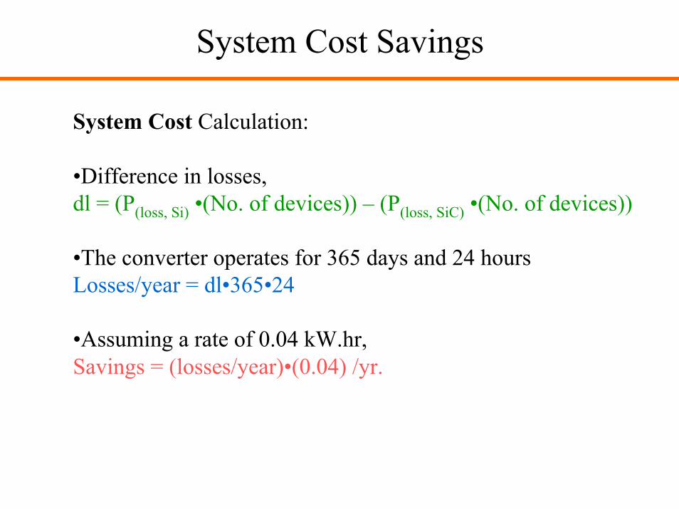
System Cost Savings
System Cost Calculation:
•Difference in losses, dl = (P(loss, Si) •(No. of devices)) – (P(loss, SiC) •(No. of devices))
•The converter operates for 365 days and 24 hoursLosses/year = dl•365•24
•Assuming a rate of 0.04 kW.hr,Savings = (losses/year)•(0.04) /yr.
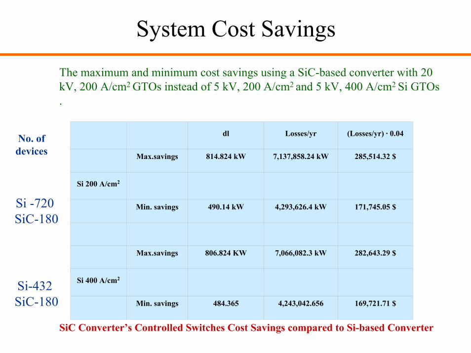
System Cost Savings
The maximum and minimum cost savings using a SiC-based converter with 20 kV, 200 A/cm2 GTOs instead of 5 kV, 200 A/cm2 and 5 kV, 400 A/cm2 Si GTOs .
dl Losses/yr (Losses/yr) · 0.04
Max.savings 814.824 kW 7137858.24 kW 285514.32 $
Si 200 A/cm2
Min. savings 490.14 kW 4293626.4 kW 171745.05 $
Max.savings 806.824 KW 7066082.3 kW 282643.29 $
Si 400 A/cm2
Min. savings 484.365 4243042.656 169721.71 $
dl Losses/yr (Losses/yr) · 0.04
Max.savings 814.824 kW 7,137,858.24 kW 285,514.32 $
Si 200 A/cm2
Min. savings 490.14 kW 4,293,626.4 kW 171,745.05 $
Max.savings 806.824 KW 7,066,082.3 kW 282,643.29 $
Si 400 A/cm2
Min. savings 484.365 4,243,042.656 169,721.71 $
No. of devices
Si -720SiC-180
Si-432SiC-180
SiC Converter’s Controlled Switches Cost Savings compared to Si-based Converter

Conclusion
• Since the losses of SiC GTO are less- the range of efficiency for SiC converter is higher. - operating cost of SiC converter is less.- reduced thermal management requirements.- device operating area (DOA) limits can be increased.- improved dynamic characteristics ⇒ less switching losses.- the ratio of number of devices in a SiC converter compared to a Si converter is less ⇒ higher voltage rating than their Si counterparts ⇒ one can afford to pay more for a SiC GTO.
• Currently GTO ratings are much lower, and their cost and losses are more than the Si thyristor. However, can be improved using SiC GTO thyristor.
• Hence, SiC close to commercialization can replace Si GTO thyrsitor.

Co-Author of Publications
1. B. Ozpineci, L. M. Tolbert, S. K. Islam, M. Chinthavali, "Comparison of Wide Bandgap Semiconductors for Power Applications," 10th European Conference on Power Electronics and Applications -EPE 2003, September 2-4, 2003, Toulouse, France.
2. B. Ozpineci, L. M. Tolbert, S. K. Islam, M. Chinthavali, "Wide Bandgap Semiconductors for Utility Applications," IASTED International Conference on Power and Energy Systems (PES2003), February 24-26, 2003, Palm Springs, California, pp. 317-321.