silicon photonics technology on soi wafers for optical...
TRANSCRIPT
Tohru Mogami
Photonics Electronics Technology Research Association (PETRA),
Japan
SOI Forum 2016
UoT
21/Jan/2016
SOI Forum 2016, UoT, 21/Jan/2016
Silicon Photonics Technology
on SOI wafers
for Optical Interconnect
1

SOI Forum 2016, UoT, 21/Jan/2016
Acknowledgements
This work is partly supported by NEDO.
I appreciate the supports of the colleagues of
“Integrated Photonics-Electronics Convergence
System Technology” Project.
2

Outline
SOI Forum 2016, UoT, 21/Jan/2016
1. What is the issues of ICT world?
2. What is silicon photonics?
3. Integrated Photonics-Electronics
Convergence System Technology
Project & W/W R&D of Si Photonics
4. SOI Issues for Si Photonics
3

Cloud Computing
Big Data Analysis
Traffic Growth in ICT Society
Data Center
Supercomputer
Sensors
Mobile phones PC
Global IP Traffic 828 EB/y, CAGR: 23%
Global Data center Traffic 4.1 ZB/y, CAGR: 31%
Tablet
SOI Forum 2016, UoT, 21/Jan/2016 4
SOI Forum 2016, UoT, 21/Jan/2016
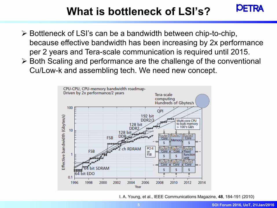
I. A. Young, et al., IEEE Communications Magazine, 48, 184-191 (2010)
What is bottleneck of LSI’s?
Bottleneck of LSI’s can be a bandwidth between chip-to-chip,
because effective bandwidth has been increasing by 2x performance
per 2 years and Tera-scale communication is required until 2015.
Both Scaling and performance are the challenge of the conventional
Cu/Low-k and assembling tech. We need new concept.
5
Outline
SOI Forum 2016, UoT, 21/Jan/2016
1. What is the issues of ICT world?
2. What is silicon photonics?
3. Integrated Photonics-Electronics
Convergence System Technology
Project & W/W R&D of Si Photonics
4. SOI Issues for Si Photonics
6

Si photonics & Building blocks
Light
source
Light
distributor
E/O
converter
Optical
wire
O/E
converter
Transmitter
circuits Receiver
circuits
Continuous light Optical signals
Electrical signals
Laser diode Silicon optical
waveguide Germanium
photodetector
Silicon optical
modulator
Light source integration
Photonics-electronics
integration
Silicon optical
splitter
SOI Forum 2016, UoT, 21/Jan/2016 7
OE device (photo-detector)
I/O device with low-loss
Wave Guide
EO device (modulator) Silicon photonics is the technology to
integrate photonic systems which
mainly use silicon as optical devices.
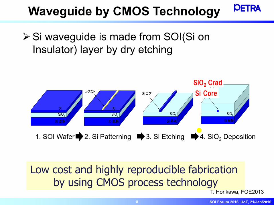
1. SOI Wafer
SiO2
Si
Si 基板
SiO2
Si
Si 基板
SiO2
Si
Si 基板
レジスト
SiO2
Si
Si 基板
SiO2
Si
Si 基板
レジスト
SiO2
Si コア
Si 基板
SiO2
Si コア
Si 基板
2. Si Patterning 3. Si Etching 4. SiO2 Deposition
SiO2
Si コア
SiO2
Si 基板
SiO2
Si コア
SiO2
Si 基板
Si Core
SiO2 Crad
Waveguide by CMOS Technology
Si waveguide is made from SOI(Si on
Insulator) layer by dry etching
Low cost and highly reproducible fabrication by using CMOS process technology
SOI Forum 2016, UoT, 21/Jan/2016
T. Horikawa, FOE2013
8

Optical Modulators with Side-wall Gratings
Fabricated optical modulators
Schematic structure
SOI Forum 2016, UoT, 21/Jan/2016
ER = 4.3 dB 5 ps/div.
ER: dynamic extinction ratio
50Gbps 50Gbps
500nm
60nm
[S. Akiyama et al, JSTQE 2013]
9
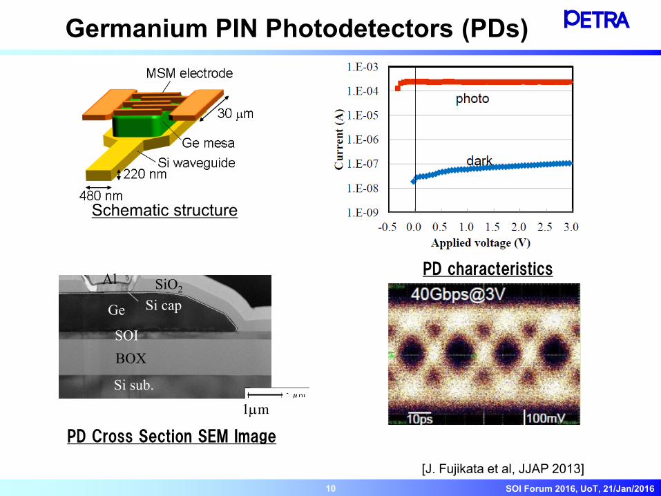
Germanium PIN Photodetectors (PDs)
Schematic structure
[J. Fujikata et al, JJAP 2013]
PD Cross Section SEM Image
PD characteristics
Ge
SOI
BOX
Si sub.
SiO2 Al
Si cap
1mm
SOI Forum 2016, UoT, 21/Jan/2016 10

SOI Forum 2016, UoT, 21/Jan/2016
200 GHz spacing 16 channel
Si-wire AWG
[H. Okayama et al., Electronics Letters 2013]
WDM is Wavelength-Division Multiplexing.
Arrayed Waveguide Grating is one of WDM devices.
Wavelength-Division
Multiplexing (WDM)
Transceiver
WDM for more high-performance
11

Outline
SOI Forum 2016, UoT, 21/Jan/2016
1. What is the issues of ICT world?
2. What is silicon photonics?
3. Integrated Photonics-Electronics
Convergence System Technology
Project & W/W R&D of Si Photonics
4. SOI Issues for Si Photonics
12

PECST Pj in FIRST Program (Finished)
1
10
100
1000
0.1 1 10 0.01
300pin-MSA
(10Gx1)
QSFP(‘08)
SNAP12(IBM ‘04)
POP4(‘05)
AOC etc.
PETIT(NEC ‘08)
Inter-Board
XFP (10Gx1)
PODAvago PETIT2(NEC‘10)
LAN・WAN
Light Peak(Intel ‘10)
Luxtera
LightWire
Luxtera
Inter-chip
1 / Transceiver Footprint (cm-2)
Bandw
idth
(G
bps)
Inter-Rack
Bandwidth density
2012
12.5Gbps/ch
6.6Tbps/cm2
2012
12.5Gbps/ch
6.6Tbps/cm2
2011
5Gbps/ch
3.5Tbps/cm2
2011
5Gbps/ch
3.5Tbps/cm2
This PECST Pj promotes research and development of these
innovative technologies for photonics-electronics convergence to
realize an on "On-chip data Center" by 2025.
Term: FY 2010~2014
SOI Forum 2016, UoT, 21/Jan/2016 13
00
2013
30 Tbps/cm2

SOI Forum 2016, UoT, 21/Jan/2016
Outline
Title: Integrated Photonics Electronics Convergence Technology Project
Sponsor: METI (FY2012), NEDO (FY2013 - ).
Organization: PETRA
Project Leader : Yasuhiko Arakawa, Professor of the University of
Tokyo
Budget: 30B¥/10 years (Plan), 2.7B¥/2013
Term: FY 2012~2021
# of researchers: 120
Member companies:
AIST, Fujitsu, Furukawa Electric, NEC, NEL, NTT, OITDA, OKI,
Toshiba
Joint research organization:
Univ. of Tokyo, Kyoto Univ., Tokyo Institute of Technology,
Yokohama National Univ., WASEDA Univ.
FOE2014, 2014/April/16 14
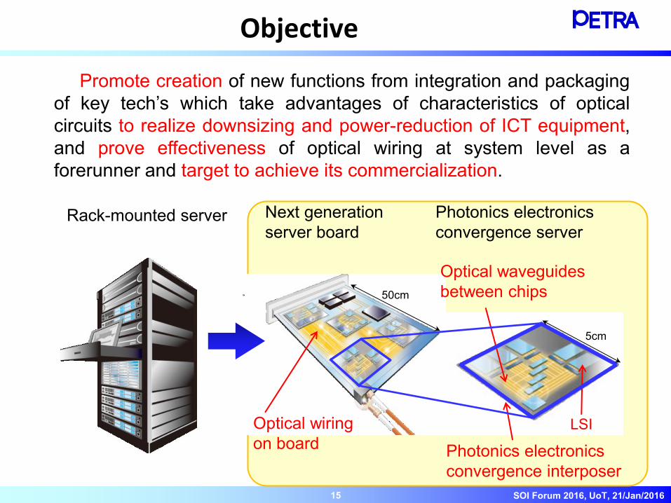
SOI Forum 2016, UoT, 21/Jan/2016
5cm
Next generation
server board
Photonics electronics
convergence interposer
50cm
Optical waveguides
between chips
LSI
Rack-mounted server Photonics electronics
convergence server
Optical wiring
on board
Objective
Promote creation of new functions from integration and packaging
of key tech’s which take advantages of characteristics of optical
circuits to realize downsizing and power-reduction of ICT equipment,
and prove effectiveness of optical wiring at system level as a
forerunner and target to achieve its commercialization.
15

SOI Forum 2016, UoT, 21/Jan/2016
2012 2014 2018 2020 2022
0.1T
0.3T
1T
10T
3T
Sy
stem
per
form
an
ce
1st stage 2nd stage 3rd stage
(bps)
Interposer w/
Photonics
Electronics
IntegrationLSI package w/
Optical cableOptical I/O
Core
AOC LSI & Package Server on package
Year
Project Roadmap
Key tech.
System tech.
Project organization to lead to commercialization based on key tech’s
Key tech ⇒ system tech ⇒ business
3 stages development w/ progressive strategies
Opt. IO core ⇒ LSI package w/ opt. cables ⇒ OE interposer
Key tech
To system
To business
Introduction to IT equipment's
System tech
FOE2014, 2014/April/16 16

SOI Forum 2016, UoT, 21/Jan/2016
2015 OFC Presentation
17

2015 OFC Presentation
18 OECC2015, Shanghai, 2015/June/28-July/2
SOI Forum 2016, UoT, 21/Jan/2016 19
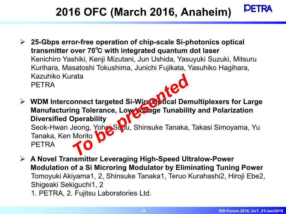
2016 OFC (March 2016, Anaheim)
A Novel Transmitter Leveraging High-Speed Ultralow-Power
Modulation of a Si Microring Modulator by Eliminating Tuning Power
Tomoyuki Akiyama1, 2, Shinsuke Tanaka1, Teruo Kurahashi2, Hiroji Ebe2,
Shigeaki Sekiguchi1, 2
1. PETRA, 2. Fujitsu Laboratories Ltd.
WDM Interconnect targeted Si-Wire Optical Demultiplexers for Large
Manufacturing Tolerance, Low Voltage Tunability and Polarization
Diversified Operability
Seok-Hwan Jeong, Yohei Sobu, Shinsuke Tanaka, Takasi Simoyama, Yu
Tanaka, Ken Morito
PETRA
25-Gbps error-free operation of chip-scale Si-photonics optical
transmitter over 70℃ with integrated quantum dot laser
Kenichiro Yashiki, Kenji Mizutani, Jun Ushida, Yasuyuki Suzuki, Mitsuru
Kurihara, Masatoshi Tokushima, Junichi Fujikata, Yasuhiko Hagihara,
Kazuhiko Kurata
PETRA

Outline
SOI Forum 2016, UoT, 21/Jan/2016
1. What is the issues of ICT world?
2. What is silicon photonics?
3. Integrated Photonics-Electronics
Convergence System Technology
Project & W/W R&D of Si Photonics
4. SOI Issues for Si Photonics
20

SOI Forum 2016, UoT, 21/Jan/2016 21
Issue: RF Loss by Si Substrate
Y. Fukuda, et al., 2001, Oki Tech. Rev.
HR sub.
(>1kΩcm)
LR sub.
(20-30 Ωcm)
Frequency (GHz)
N. Li, et al., 2014, Symp on VLSI Tech & Circuit.
Transmission loss by Si substrate occurs in metal
interconnects with GHz signals.
Low-loss interconnect requires high-resistance Si
substrates, as well as Si substrates in SOI wafers.
However, there are no 12 inch high-resistance SOI
substrate.
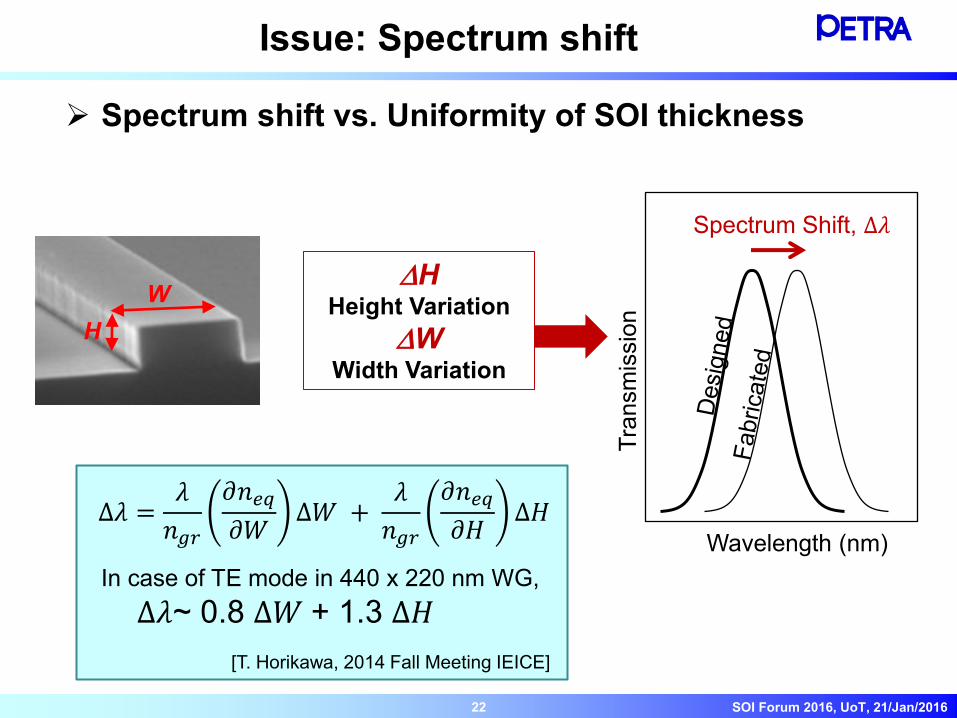
Wavelength (nm)
Spectrum Shift, Δ𝜆
Tra
nsm
issio
n
DH Height Variation
DW Width Variation
Issue: Spectrum shift
SOI Forum 2016, UoT, 21/Jan/2016
Spectrum shift vs. Uniformity of SOI thickness
22
∆𝜆 =𝜆
𝑛𝑔𝑟
𝜕𝑛𝑒𝑞
𝜕𝑊∆𝑊 +
𝜆
𝑛𝑔𝑟
𝜕𝑛𝑒𝑞
𝜕𝐻∆𝐻
In case of TE mode in 440 x 220 nm WG,
∆𝜆~ 0.8 ∆𝑊 + 1.3 ∆𝐻
[T. Horikawa, 2014 Fall Meeting IEICE]
W
H
SOI Forum 2016, UoT, 21/Jan/2016
Summary
For ICT systems, one of today’s bottlenecks is the
bandwidth b/w LSI’s. Optical interconnect has the
advantage of the wider bandwidth characteristic than
metal electrical one.
Silicon photonics is the technology to integrate photonic
systems which mainly use silicon as optical devices.
Si photonics is a good application of More Than Moore.
23