simple relations derived fom a phased-array antenna made...
TRANSCRIPT

506 I&&& 1 KAlVbHL'l 1 UlVb UfV A I V 1 L I V l V A b A l V U r"nUl-ACTHllUl\' JULY
[SI Frost, A. D., Surface waves in Yagi antennas and dielectric [15] Rlatkins, D. A., Topics in ELectrmzug?zetic Theory. New York: waveguides, Tech Rept AFCRC-TR-57368, Dept. of Physics, [Viley, 1958. Tufts University, &ledford, Mass., 1957.
[9] Serracchioli, F., and C. A. Levis, The calculated phase velocity [161 Zucker, F. J., Electromagnetic boundary wa\-es, an introduction.
Rept .IFCRL-63-165, USAF Cambridge Research Lab., Bed- of long end-fire uniform dipole arral-s, IRE Trans. on d t z t e n m s ford, Mass., Jun 1963. and Propagation (Special Supplement), vol AP-7, Dec 1959, [I;] Slater, J. C., Xicrowave Electronics. Kew York: McGraw-Hill,
[lo] Zucker, F. J., Theory and applications of surface Lvaves, Nuovo [18] Cullen, A. L., Proc. Inst. Elec. Engrs., vol 101, pt 4, 1954, pp czmento (Microwave Optics Symposium Issue, Supplement 3), vol9, September 1961.
225-231. [19] Chu, E. L., and W. W. Hansen, J., AppZ. Phys., vol 18, Nov
[Ill Brown, G. H., and R. I\,'. P. King, High-frequency models in 1947, pp 996-1008.
[12] Brillouin, L., Hhve Propagation itz Periodic Structures. Kew antenna investigations, Proc. IRE, ~0122, Apr 1934, pp 457480. [20] Sengupta, D. L., On the phase velocity of wave propagation
along an infinite Yagi structure, IRE Trans. o n Antennas and
[13] Collin, R. E., Field Theory of Guided Waves. Kew York: Mc- [21] King, R. IT. P., Linear arrays: currents, impedances, and fields, York: Dover, 1953. Propagation, vol AP-7, Jul 1959, pp 234-239.
[14] Rao, B. Rama, Theoretical and experimental studies of an- Graw-Hill, 1960. I , IRE Trans. 012 A n t e m a s and Propagation (Special Supplement),
vol AP-7, Dec 1959, pp SMGS4.57. tennas and arraJ-s in a parallel-plate region, Part IV-1i'ax-e [231 Mailloux, R., A unification of antenna-theory and wave-theory:
region, Scientific Rept 2, ser 3, Cruft Lab., Han-ard UniversitS-, propagation along infinite Yagi-type arraS-s in a parallel-plate infinite Yagi-Uda arrays, Tech Rept 451, Cruft Lab., Harvard
Cambridge, Mass., Mar 1963. Vniversity, Cambridge, Mass., Jun 1964.
pp s424-s434. 1950, pp 17S177.
Simple Relations Derived from a Phased-Array Antenna Made of an Infinite Current Sheet
Absfract-The simplest concept of a phased array is an W t e planar current sheet backed by a reflecting boundary. The electric current sheet, or resistance sheet, is the limiting case of many small electric dipoles, closely spaced, and backed by an open-circuit boundary. If this array is viewed as a receiver, a plane wave incident on the array at some angle (e) meets a boundary resistance varying in proportion to cos 8 for angles in the H plane, and l/cos e for angles in the E plane. If the array is matched at broadside (O=O), the corresponding reflection coefficient has the magnitude (tan $e)*.
While the electric current sheet is realizable, the open-circuit boundary is not. However, a magnetic current sheet can be simu- lated by a conductive sheet with holes utilized as magnetic dipoles, such a sheet providing the backing equivalent to a short-circuit boundary. The latter case is related to the former by electromagnetic inversion or duality. Therefore, an incident plane wave meets a boundary conductance varying in proportion to cos tJ for angles in the E plane, and l/cos 0 for angles in the H plane. The predicted behavior is vedied qualitatively by tests of such a model with elements of a practical size.
The derivation is based on the principle of dividing the space in front of the array into parallel tubes or waveguides, one for each element cell in the sheet or array. This is one of the principles pub- lished by the author in 1948. A related principle enables the simu- lation of an infinite array by imaging a few elements in the walls of a waveguide. This latter principle is utilized for making tests of the array.
Manuscript received September 28, 1964; revised February 4, 1965. This paper was originally presented at the IEEE Symposium on Antennas and Proparation, Sentember, 1964.
The author is President of \S.rheeler Labs., Inc., Great Seck. N. Y.
I . INTRODUCTION PLANAR ARRAY of many radiating elements is used t o develop a narrow pencil beam. The connections between the elements and the send-
ing or receiving circuit are phased to control the beam angle of deflection from broadside (the "scan angle"). This is the type of antenna commonly called a "phased array," implying beam steering by electrical phasing without mechanical motion of the array.
This type of antenna introduces an unusual problem of design: the variation of element impedance with scan angle. This variation is caused by the inherent coupling of the elements, which contributes to the apparent im- pedance of each element in a manner dependent on the phasing required for the scan angle. With phasing for wide-angle scanning, the impedance variation from this cause becomes substantial and should be taken into ac- count, along with the variation from other causes such as the frequency bandwidth.
There have been various studies of the element im- pedance variation with scan angle. Some are based on laborious computation of an array of many elements [ 5 ] , ['i], [12], [13]. Others are based on the concept of an infinite array [2], [6], [SI, [14], [l'i], [IS], [21]. This latter concept has been found by the author to offer the best basis for the design of an element for use

1965 Wheeler: Phased-Array Antenna from an Infinite Current Sheet 507
a t all locations in a finite array of many elements. More- over, i t offers the only evaluation that is independent of the number of elements. Therefore, there is a particular interest in the behavior of an element in an infinite array.
In general, the variation of element impedance with angle depends on the “fine structure” of the element, and on the arrangement of elements in the array. However, there is a hypothetical array which avoids any question of fine structure. This is the array that is formed of an infinite current sheet, representing elements so small and so closely spaced that the fine structure is not resolved. On the basis of such an array, there is found a simple derivation for impedance variation with angle, which is inherent in arrays fitting into a certain pattern. Further- more, i t is found that some practical types do fall into this pattern, so the conclusions from this hypothesis are useful in practice.
I t is the purpose of this paper to describe the hypo- thetical array formed of an infinite current sheet, to derive its impedance variation with angle, and to in- troduce some corollary concepts, such as the “ideal element pattern,” which theoretically would avoid the implement variation.
The scope of this treatment is limited to the infinite planar array, having a well-defined planar face (ground plane), which separates the radiation region (free space, in front) from the associated circuits (shielded, behind). A practical example is an array of radiating holes in a sheet of conducting material (metal).
I t is noted that the apparent impedance of the ele- ment, as formulated here, is the “active impedance” tha t would be seen looking out of one element with all the other elements excited in the phase required for the scan angle.
11. SYMBOLS
MKS rationalized units. 1 =effective length of small electric dipole. a =element spacing in square array.
A =a2 =area of element cell in square array. B=scan angle from broadside. X = free-space wavelength. E = electrivity (electric permittivity)
1-1 = magnetivity (magnetic permeability) H = magnetic field intensity (Ajm). E =electric field intensity (V/m). I= current in electric dipole.
current sheet (X/m). H , = magnetic field intensity adjacent to electric
I , = electric current density in sheet (a/m). F(0) =relative field intensity in radiation pattern of
R= radiation resistance of electric dipole in active
R, = 377 ohms = wave resistance across square area
R,= resistance across square area of sheet.
isolated element.
array phased for some angle.
of wavefront in free space.
G = radiation conductance of magnetic dipole (across a slot) in active array phased for some angle.
p = voltage-reflection coefficient a t face of array. sub-c = free space sub-o = broadside (0 = 0). sub-s =sheet.
sub-m =plane of magnetic field ( H ) . sub-e =plane of electric field ( E ) . sub-i = ideal. sub-k = Huygens source.
111. THEORETICAL BACKGROUXD
The concept of the infinite array was introduced by the author in 1948 [2], long before the recent intensive work on phased arrays with beam steering. That publi- cation showed the opportunity for simple computation of some properties of a radiating element in an infinite array. This approach had been suggested by the theory of such an element in a waveguide. Now it turns out that the same principle is applicable to phased arrays. Moreover, it is found that the experimental design of an element for a phased array is facilitated by imaging a few elements in waveguide walls to simulate an infinite array [IT], [2O], [23], [ X ] .
-4s an introduction to the present discussion, Figs. 1 and 2 are reproduced from the 1948 publication. Figure 1 shows an infinite planar array of electric dipoles in a square arrangement in a plane with free space in front and “open circuit behind.” This is the same basis to be used for the infinite current sheet. Fig. 2 shows a modi- fication of the same to form an array phased for an oblique angle of radiation. This is a special case of a phased array, in which adjacent elements are phased in opposition; a condition that is most simply simulated by the metal walls of a rectangular waveguide. (The same publication also describes the simulation of an infinite array in a rectangular waveguide, with oblique angles of radiation.)
Among the formulas in that publication, there are two that form the background for the present discussion. Referring to Fig. 1, the radiation resistance of each ele- ment is given as
Ro = R,12/a2 = R,12/4. (1)
Referring to Fig. 2, for oblique radiation at an angle 0 from broadside, in the H plane, the radiation resistance happens to be given for a pair of directions (+e ) . Tak- ing one-half of this for one direction,
R, l2
cos 0 a2 R=- - .
This forms an introduction to the angle variation of mpedance that is to be derived. In this case, the radia-
tion resistance increases with angle from broadside. In the 1948 publication, some reliance is placed on

508 IEEE TRANSACTIONS OM ANTEhWAS AhiD PROPAGATION Julg
earlier derivations of the radiation resistance of an electric dipole in a rectangular waveguide. The com- pletederivationcan be described briefly with reference to the tubes of radiation in front of the array, as shown in Figs. 1 and 2. In the broadside direction (@=O), shown in Fig. 1, the tubes are square and are bounded by hypo- thetical image planes. The wave resistance between top and bottom of each square cell (u2) is that of free space (Rc). The electric dipole (of effective length = I ) is coupled to this resistance by an effective transformation ratio (Z/u), so its radiation resistance is proportional to the square of this ratio, as appears in formula (1). In an oblique direction (e), as shown in Fig. 2, each tube is decreased in width by the projection cosine, so the re- sistance of the tube and of the dipole is increased by the factor l/cos 0.
I t is noted that this simple computation for an in- finite array is based on real power, and, therefore, only the resistance component is given. In general, there is also a variation of the reactance component, so that the impedance variation is the resultant of both components.
H PLANE
I I I
I I I I
I I I
E PLANE
Fig. 1. ;in infinite planar array at the boundary of half-infinite space. (a) Plan. (b) Elevation.
H PLANE
Further theoretical background is found in more re- cent publications, which will be reviewed in a later section of this paper.
IV. THE INFINITE CURRENT SHEET
The present discussion is to be based on an infinite current sheet. There are two kinds of current sheet that may be assumed, electric and magnetic. The former is conceptuallq. the easier, because an electric conductor is within our experience. Therefore i t will be utilized for the derivations. On the other hand, the magnetic cur- rent sheet (and not the electric) is found to be realizable in the required environment of the array, so i t will be relied on for experimental verification.
Figure 3 shows the basis for a planar phased array made of an electric current sheet. The baseline in Fig. 3(a) is the scan-plane projection of the plane of the array. -\hove the line is represented the radiation re- gion (free space) in front of the array. Below the line is assumed t o be an “open-circuit” reflector behind the array ( E = 0, p = w ). The latter region is not physically realizable, but is conceptually simple; i t is carried over from Figs. 1 and 2.
The electric current sheet is in the plane of the array. I t has a current density 1, of uniform amplitude, but phased for radiating a plane wave in a direction a t a n angle 0 from broadside. The current density is associated with a magnetic intensity H, of equal amplitude and
H PLANE E PLANE
MAGNETIC ,/ ELECTRIC ,’ WALL 7’ < WALL?‘ 0 H
Is Is
(a) Plane of scan, showing current sheet and magnetic fields.
a a
r - - - - - --1 r - - - - - - - T I I I
(b) Plane of array, showing element cell of current sheet and equivalent current element.
Fig. 3. .An idealized model of a planar array, made of an electric current shzet.
\I
Fig. 2. The same array phased for an oblique angle of radiation.
1YOO w neem: rnmed-Army Antenna p o r n an Infinate G‘urrmlt Sheet 509
phase, but crossed in space. In the radiation region, the H plane and E plane are determined to include, respec- tively, the H, and I , vectors. The scan angle I3 may be in either of these planes, as shown.
Figure 3(b) shows the face of the array, the infinite current sheet being exemplified by a square cell of area A =d. For some purposes, there will be used also the illustrated concept of a small electric current element, or electric dipole, equivalent to a small cell. These are said to be equivalent if they have equal moment. If the moment of the latter is ZI, as indicated, the condition for equivalence is
I1 = a(a1,) = L41,. (3)
For the broadside direction of radiation (I3 = 0), ob- tained by uniform phase over the array, the radiation resistance Ro of this element is given by formula (1).
The current sheet may have any value of uniform surface resistance R, (the resistance across any square of the surface). For present purposes, i t is assumed to be “matched” to free space for broadside radiation, so R,=R, (377 ohms, the wave resistance across a square area of wavefront in free space).
V. THE VARIATION OF IMPEDANCE WITH SCAN ANGLE Since the receiving viewpoint may be conceptually
simpler, i t will be taken first for deriving the variation of impedance with scan angle. This derivation will be based on Fig. 3(a), showing the two principal planes of scan angle, the H plane and the E plane. Any reflection from the face of the array, as will be derived, appears in the form of a beam radiated at the opposite angle from broadside.
Referring to an oblique angle of scanning in the H plane, we have a situation similar to Fig. 2. The incom- ing wave sees a section of current sheet which is wider han the section of wavefront, so the wave appears to
be reflected by a resistance that is lesser in the ratio, cos 13. The resulting voltage-reflection coefficient is nega- tive :
cos e - 1
COS e + 1 Pm = = - (tan+e)z.
Referring instead to an oblique angle of scanning in the E plane, we find an opposite situation. The incom- ing wave sees a section of current sheet which is longer than the section of wavefront, so the wave appears to be reflected by a resistance that is greater in the ratio, l/cos 0. The resulting voltage-reflection coefficient is positive :
Changing over to the sending viewpoint, we may derive the same relations, but naturally the reflection
coefficient will be reversed. Here we refer also to the equivalent current elements in Fig. 3(b).
The method is given in the author’s early paper on this subject [ 2 ] , here represented by Figs. 1 and 2. The space in front of the array is partitioned by hypo- thetical waveguide walls and the radiation resistance of cach clcmcnt is formulatcd. Referring t o Fig. 3(a), these walls are located by projecting the element cell in the beam direction determined by the array phasing. The nature of the walls is determined by the require- ment for imaging the fields of a uniform plane wave: the walls parallel to the H field are “electric” walls, or “short-circuit” boundaries ( E = oc , p = 0) ; and the malls parallel to the E field are “magnetic” walls, or “open- circuit” boundaries (E = 0, p = a).
From (1) , the radiation resistance of each element is known for broadside phasing (Ro for I3 = 0). Changing to the phasing for an oblique angle modifies the situation in two respects. First, the area of wavefront is decreased by the factor cos 0, increasing the resistance by the factor l/cos 8, as in (2). Second, the radiation pattern of the element may affect the relative amount of radia- tion in the beam direction. The latter effect is to be for- mulated here.
The radiation pattern of a small electric dipole has the following dependence on the angle I3 in Fig. 3.
H plane: E/Eo = Fm(e) = 1 (6)
E plane: E/Eo = F,(O) = cos 0. (7)
This is the familiar “doughnut” pattern, or specifically the half of this pattern that is located in front of the array. These factors may be regarded as foreshortening of the element length by projection on the wavefront. The effect on the radiation resistance is naturally pro- portional to the square of this factor.
The resulting variation of element resistance with an- gle is given by the following formulas, which are essen- tially similar to some derived by Stark [6].
1 H plane: R/Ro = - [Fm(f3)I2 = l/cos 0 (8)
COS e 1
E plane: R/Ro = - [ F e ( e ) ] 2 = cos 8. (9)
As would be expected from the principle of reciprocity, these ratios are the inverse of those derived from the receiving viewpoint. Each of the corresponding reflec- tion coefficients is merely reversed.
The factor l/cos 8, which appears in (8) and (9), may be inferred from another viewpoint in transmission. Let us consider a finite planar array of many elements, so large that the beam width is a small fraction of one radian. In any particular plane of scan, the aperture width projected in the beam direction is proportional to cos 8 , so the beam width is inversely proportional to this ratio. The power in the beam is proportional to the
COS e
factor F2 in the beam direction, and also to the beam width. The latter introduces the factor l/cos 0 in the radiation resistance.
From the sending viewpoint, the reflected power is returned to the generator, or may be absorbed in an intervening “isolator.” In the case of a generator matched to the element broadside resistance Ro, the net result of the reflection is to decrease the radiated power below the “available” power by the factor (1 - I p I ’).
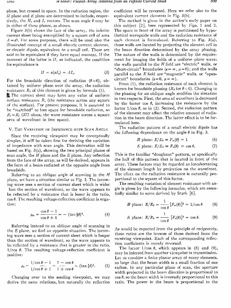
Figure 4 shows the variation of element resistance and reflection coefficient with scan angle in the H and E planes. The polarity of p , in Fig. 4(a), is given for the electric dipole, as in Fig. 3(b).
la) l b )
Fig. 4. The variation of reflection Kith scan angle, in the idealized model. (a) For the case of electric dipoles, from the sending view- point. (b) For either kind of dipoles, from either viewpoint.
In general terms, the same derivation is applicable to the inverse case of a magnetic current sheet, with transformation by the principles of duality. This means interchanging H and E , interchanging open-circuit and short-circuit reflector, interchanging resistance R and conductance G (or inverting R), and interchanging voltage and current-reflection coefficients (or reversing the sign of the voltage-reflection coefficient), The radia- tion pattern of a small magnetic dipole (or slot in a metal sheet) is as follows,
E plane: E/Eo = Fe(B) = 1 (10)
H plane: E/& = F,(O) = cos 8. (1 1)
The resulting variation of element conductance is as follows,
1 cos 0
E plane: G/Go = - [Fe(0)l2 = l/cos 0 (12)
1 H plane: G/Go = - [Fm(f3)I2 = cos 8.
COS e Of greatest importance is the fact that the magnetic
current sheet can be simulated in a physical structure. A metal sheet can be used as the required short-circuit reflector, and holes in the sheet can be used to simulate the required magnetic dipoles as radiating elements. Such a practical structure will be described further on.
The current sheet has only resistance and no reac- tance, so the simple theory gives the entire variation of
impedance with angle. 14’hen approximated by an array of elements of appreciable size and spacing, there is a departure from this simple rule. Usually, the resistance variation is somen-hat different, and there is also appre- ciable variation of reactance.
In general, the angle from broadside either increases or decreases the radiation loading of the element, from the sending viewpoint. The radiation loading of an electric dipole is proportional to resistance, while that of a magnetic dipole is proportional to conductance. From the formulas given, the following conclusions can be drawn.
Variatiolt of radiation loading by increasing angle (0)
E dipole increasing decreasing
Plane of angle ( e ) Radiating elentent
H plane E plane
M dipole decreas-ing increasmg
VI. THE IDEAL ELEMENT PATTERN
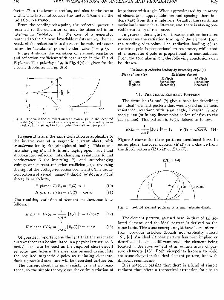
The formulas (8) and (9) give a basis for describing an “ideal” element pattern that would yield an element resistance invariant with scan angle, likewise in any scan plane (or in any linear polarization relative to the scan plane). This pattern is F,(B), defined as follows.
Figure 5 shows the three patterns mentioned here. In either plane, the ideal pattern (E‘H’) is a change from the dipole pattern ( H to H’ or E to E’).
0
Fig. 5. Isolated element patterns of a small electric dipole.
The element pattern, as used here, is that of an iso- lated element, and the ideal pattern is derived on the same basis. This same concept might have been inferred from previous articles, though not explicitly stated [SI , [6]. An ideal element pattern has been implied or described also on a different basis, the element being located in the environment of an infinite array of pas- sive elements [l8]. Both viewpoints happen to yield the same shape for the ideal element pattern, but with different significance.
I t is noted in passing that there is a kind of simple radiator that offers a theoretical attraction for use as

1965 Wheeler: Plmed-Arra.y Antenna from a.n Infinite Current Sheet 511
an element in an array. I t is the “electromagnetic di- pole” or “Huygens source” [l], [3], [4], [g], [ll]. I t is formed by crossed superposition of an electric dipole (or current element) and a magnetic dipole (or current loop) radiating equal (maximum) fields in one direction (the axis). This gives the same amplitude of field in all planes through the axis, namely,
I Fh(e) I = +(I + COS e) = (COS +e)’. (15)
This has a cardioid shape which is a close approximation to the ideal shape (14). Aside from its favorable pat- tern, i t has some peculiarities that require further study before it can be used as an element in an array. 1) It is difficult to realize in a physical structure. 2) I t is a two- port for each linear polarization, as distinguished from the usual one-port. 3) Its pattern would be destroyed by any reflector behind the element. In the meantime, this type of radiator offers some intriguing opportu- nities for theoretical studies.
VII. A PRACTICAL STRUCTCRE -4s previously mentioned, the relations derived here
are applicable to a practical structure simulating a mag- netic current sheet backed b); a short-circuit reflector. Figure 6 shows such a structure. The array is formed of a metal sheet with the elements radiating through holes in the sheet. It has some properties in common with the arrays of slots, as exemplified in the studies by Rabinowitz, Edelberg, and Oliner [SI, [8].
There is a periodic array of holes in either of the two forms that are useful. Figure 6(a) shows a square array, which is the simplest form. Figure 6(b) shows a tri- angular array, which is still simple and offers some practical advantages. Also it gives the closer approxima- tion to a current sheet, for the same separation of adja- cent elements. Figure 6(c) shows a cross section of either form through a “cardinal” plane (C-C).
The resistance sheet in this presentation is isotropic. Following this concept here, each element hole is made circular, and is backed by a circular waveguide. Simula- tion of the current sheet requires that the hole diameter and center-to-center spacing be sufficiently small in terms of the wavelength, so that this “fine structure” cannot be “resolved” by the wave. This condition is nearly satisfied if these dimensions are much less than one-half wavelength, whereas dimensions of this order are required in practice. In the circular waveguide, the TE-11 mode is to be utilized. Its propagation requires dielectric loading in this diameter. Such loading may be provided by spaced circular disks of high dielectric con- stant, to avoid proportionate loading of the undesired TM-01 mode [19].
This structure will handle any polarization. In prac- tice, i t requires impedance matching over the required frequency band, which can be approximated by insert- ing obstacles in the circular waveguide. There remains
000
( b l C -
Fig. 6. An array of circular holes in a metal sheet. (a) Square array. (b) Triangular array. (c) Cross-section in cardinal plane C-C, showing dielectric-disk loading in circular waveguide.
the impedance variation with angle, which is the subject of this monograph.
17111. EXPERIMENTAL VERIFICATION
The author’s laboratory has made tests of a practical array utilizing such a structure. infinite array has been simulated by imaging a few elements in the plane walls of a waveguide [17], [ZO] , [23], [24]. Then the reflection coefficient has been measured from the 1. rlew- point of reception.
The experimental structure is a triangular array, as shown in Fig. 6(b). The hole diameter is 0.45 wavelength, and the center-to-center spacing is 0.60 wavelength. The dielectric loading is sufficient t o lower the TE-11 cutoff frequency down to about l/d? or 0.7 of the operating frequency. Figure 7 shows on the reflection chart the voltage-reflection coefficients for several scan angles. Each point is observed in an individual wave- guide to simulate the particular angle in an infinite ar- ray.
In this experiment, there is no attempt to provide impedance matching at the array face for broadside phasing, which is assumed in the theoretical derivation. Each waveguide is provided with a matched termination t o assure a pure traveling wave in reception.
On the reflection chart, Fig. 7, the two extreme points represent a large scan angle of 56” in the cardinal plane, C-C in Fig. 6(b), with E or H vector in this plane as indicated. The intermediate point represents a small scan angle of 29”, so i t is not much different from 0”

512 IEEE TRANSACTIONS O N ANTEhWAS AND PROPAGATION July
Fig. 7. The coefficient of reflection from the face of an array, at various angles, from the receiving vien-point.
(broadside); this angle happens to be in the inter- cardinal plane (30" from C-C) with H in this plane. These angles are well within the limits out to which the array would develop a single beam free of grating lobes.
On this chart, the scale of normalized resistance is marked in the region of interest.
The relation of the three points on the reflection chart is, roughly, what would be expected from the simple theory based on a magnetic current sheet, off-center, though as not matched for broadside. 1) The points are near the real axis of impedance and reflection coeffi- cient. 2) The resistance is higher for E in the scan plane. 3 ) The extreme points are separated slightly more than the predicted closest resistance ratio, the lowest value being roughly 0.22 times the highest value, as compared with (cos 56")2 = 0.31. 4) The intermediate point is not far from the ratio mean of the extreme value of re- sistance.
Regarding the experimental points more critically, i t is reasonable to say that all the discrepancies ma>- be caused by the size of the element, specifically the hole diameter and the spacing. The resistance variation is close to the predicted amount and there is little varia- tion of reactance. At least, there is qualitative agreement and a fair approximation to quantitative agreement.' I t is remarkable that it has been possible to measure the behavior of a practical element in an environment simu- lating an infinite array.
More recent theoretical and experimental studies have evaluated the reflection coefficient from the transmitting viewpoint. From this viewpoint, the phase of reflection varies with scan angle and polari- zation, as affected mainly by element spacing.
IX. HISTORICAL EVOLUTION OF THE CONCEPTS
Having developed a simple picture of the array reflec- tion, as it varies with scan angle, we shall review the evolution of ideas that has led t o this result. We shall pass over the historic studies of the coupling between elementary antennas, which enabled the detailed com- putation of finite arrays, since this method becomes unduly laborious for a large number of elements. The present objective is to evaluate the typical or average behavior of an element in a very large planar array, the number of elements being in the range from 10 by 10 = 100, UP to 100 by 100 = 10,000.
The viewpoint of the infinite array was introduced by the author's publication of 1948 [2]. In a unified presen- tation, it showed the identity of behavior of a radiating element in a waveguide with plane walls and in an infi- nite array. I t then applied the waveguide viewpoint for computation of the element radiation resistance in closed form, avoiding the summation of a doubly infinite series. Inherent in this presentation were some more specific principles whose significance was not appreci- ated until Iater.
The infinite array which received most attention in that monograph was the planar array phased for a broadside pencil beam, Fig. 1 here. For theoretical purposes, this was identified with a nonphysical rectan- gular waveguide, so the element behavior in the array mas found to be different from what had previously been computed for practical waveguides. On the other hand, the infinite array which was shown phased for oblique radiation, Fig. 2, was intended only for its theoretical interest in relation to the well-known wave behavior in physical rectangular waveguides. At that time, the author did not envision the future oppor- tunities for an array with electrical phasing for beam steering without mechanical motion. However, the be- havior of such a phased array was inherent in the theoretical derivation for waveguides, as seen here (2).
About ten years later, the growing interest in phased arrays began to be reflected in the published literature. There were three principal sources of publications re- lated to the present subject, namely, S. Edelberg and -4. A . Oliner [SI, P. S . Carter, Jr. [ 7 ] , and J. L. 411en [IS]. Of special significance, also, were the reports of S . J. Rabinowitz [SI, J . L. Allen [12], and L. Stark [6]. X11 of these sources were concerned with the variation of element impedance with scan angle.
Among the recent publications, the one most closely related to the present subject is that of Edelberg and Oliner [SI. They extend the waveguide analogy to a rectangular array of holes in a metal sheet, and to any scan angle. ITrhile their presentation is complicated by the finite dimensions of the element cell and the hole, one can glean from it the simple relations that are

1965 Wheeler: Phased-Array Antenna from an Infinite Cument Sheet 513
presented here, for the limiting case of small elements and close spacing, simulating the magnetic current sheet.
The concept of an ‘‘ideal” element pattern has not yet been published in clear and explicit terms. In the formulas of Rabinowitz [j], and in those of Stark [6], the radiation resistance of an element is seen to depend on the radiation pattern of an isolated element (includ- ing its reflector). From these formulas, one might infer that an element having a particular pattern (14) would cause the radiation resistance to be invariant with scan angle. An attempt is made here to present this topic clearly. (This concept of isolated element pattern should not be confused with the different concept of array ele- ment pattern, the latter being effective in the array environment [HI. It happens that the ideal pattern has the same shape in both cases.)
While beyond the scope of this report, it is natural to speculate on the significance of the impedance varia- tion with a current sheet, and how it might be decreased in practice. The current sheet is a thin array, having no depth in the transition face between the circuits and the radiation region. One approach for decreasing the impedance variation involves structural depth with dimensional controls, such as projections in front, or the spacing between dipoles and reflector, or the addi- tion of interconnecting circuits behind the array [ls], [22]. ilTe may infer a principle that the simple relations are associated with a thin array of small elements, and that element size or structural depth offers some oppor- tunity for departure from these relations.
The problems of evaluating an array are those of computation, on one hand, and of measurement, on the other. Since the computations were greatly simpli- fied by the analogy between an infinite array and a waveguide, i t should not be surprising that a similar approach has been found invaluable in measurements. This application is naturally restricted to the cases where the hypothetical waveguide is physically reliable. Since 1960, the author and his associates have been ex- ploring the discrete cases where a physical waveguide is available for simulating the behavior of an infinite array [17], [20], [23], [ H I . Rectangular waveguides have been utilized for square and triangular arrays, and there are some cases of the latter type where a triangu- lar waveguide is particularly useful.
The concept of an element in an infinite array has been acquiring stature also as the sound basis for de- signing a practical element for use in a large array of many elements. The element impedance in an infinite array appears to be centered in the range of element impedance at all locations in the finite array. This practical utility excites further interest in the concept.
I t is common experience in science, that the ultimate simplification in concepts comes as a culmination of more complicated studies. The present topic appears to
be an example of this principle, and an attempt has been made to reduce it to the simplest terms.
X. CONCLUSIOK The current sheet is a highly simplified conceptual
model of a phased array. I t is used as the basis for deriving some simple relations. One is the variation of element impedance and reflection coefficient with scan angle. Another is the ideal isolated-element pattern that would make the element radiation resistance in- variant with angle.
The derivation relies on the principle that an element in an infinite array behaves like one in a waveguide with properly defined walls, as presented in the author’s monograph of 1948.
In this model, the reflection coefficient varies with the scan angle, oppositely for the H or E vector in the scan plane. The predicted variation has been verified qualita- tively by tests of an array approximately simulating a magnetic current sheet.
L~CKNOWLEDGMENT
The author’s organization has been engaged in active work on the design of phased arrays under the direction of Bell Telephone Laboratories. Tha t work has pro- vided the stimulus for this study, and the author is particularly grateful to R. L. Mattingly and P. H. Smith for their encouragement.
The staff of Wheeler Laboratories has participated in this study in various wag-.s, particularly in helpful discussions and the experimental verification, for which the author wishes to express his appreciation.
REFEREKCES 111 S. A. Schelkunoff, Electromagnetic Waves. Princeton, X,. J.:
Van Nostrand, 1943, pp. 354-355. (Huygens source, cardlold patterns.)
[2 ] H. -4. IVheeler, “The radiation resistance of an antenna in an infinite array or waveguide,” Proc. IRE, vol. 36, pp. 478488, April 1948.
[3] E. C. Jordan, Elecfronzngnetic Waves and Radieting Systems. Englewood Cliffs, N. J.: Prentice-Hall, 1950, pp. 521-523. (Huygens source, cardioid pattern.)
[4] S. A. Schelkunoff and H. T. Friis, Antennas-Theory and P r u - tice. Yew York: IViley, 1952, pp. 531-523. (Huygens source,
[SI S. J. Rabinowitz, “The conductance of a slot in an array an- cardioid pattern.)
tenna,” M.I.T. Lincoln Lab., Lexington, Mass., Tech. Rept. 192, December 31, 1958. (Rectangular array of slots in metal sheet. Computation by summation of series. Relation between element pattern and variation of radiation conductance.)
161 L. S t y k , “Radiation impedance of a dipole in an infinite array, Hughes Aircraft Co., Fullerton, Calif., Tech. Rept.
by first term of summation. Relationship between element pat- FL 60-230, May 1, 1960. (Impedance matrix, resistance given
tern and variation of element resistance.) Submitted to IEEE Trans. on Antenrzas and Propagation.
[7] P. S. Carter, Jr;,, “Mutual impedance effects in large beam scanning arrays, IRE Trans. on Antennas a.7d Propagation, vol. AP-8, pp. 276-285, May 1960. (Comparison between finite
[8] S. Edelberg and A. A. Oliner, “Mutual coupling effects in and infinite width of array.)
large antenna arrays: Part I-Slot arrays,” IRE Trans. on Axtennus atzd Propagatw?z, vol. -4P-8, pp. 286-297, Ma); 1960.
to a single mode.) (i1;aveguide viewpoint, starting with all modes and simplifying
[9] J . D. Hanfling, “Mapping of the far field polarization of an-
514 IEEE TRANSACTIONS O N AArTEhrlVAS AhTD PROPAGATION J d Y
tennas by the stereographic projection,” 1LI.S. thesis, Polytechnic Institute of Brooklyn, New York, N. Y. , June 1960. (Crossed Huygens sources for unidirectional radiation with pure circular polarization, realization by electric dipole and current loop.)
[lo] J. L. Allen, et a]., “Phased array antenna studies, 1 Jull- 1959 to 1 J u l s 1960,” M.I.T. Lincoln Lab., Lexington, hIass., Tech. Rept. 228, ASTIA4 Doc. 249, 470, Xu, Oust 1960.
[ l l ! H. Jasik, “Fundamentals of antennas,” in Antenna Engineering Handbook. Ken- York: \$?ley, 1961, ch. 2, pp. 7-10. (EhI dipole cardioid pattern, realization by electric dipole and current loop.)
[12] J. L. Allen, et al., “Phased array radar studies, 1 July 1960 to 1 July 1961,” M.I.T. Lincoln Lab., Lexington, RIass.. Tech. Rept. 236, November 1961. (Computed variation of reflection with angle for se\-eral cases of dipoles with reflector.)
[13] -, “Gain and impedance variation in scanned dipole arrays.” IRE Tra zs. on .4ntennas and Propagation, vol. AP-10, pp. 566- 572, September 1962. ,Many references.)
[14] H. A. \<heeler. “Principles of phased arrays,” \\heeler Labs., Great Keck, L. I., N. Y., P-1116, May 1963. (Xotes for three
[15] P. \%’. Hannan. D. S. Lerner, and G. H. Knittel, “\Vide-angl: seminars, diagrams, many references.)
impedance matching calculated for a phased arra?- antenna, 1963 G-AP Sywap. Digest, pp. 228-233. (Achieved by intercon- necting circuits behind the array.)
[16] J. L. Allen, “The theory of array antennas,’ M.I.T. Lilcoln Lab., Lexington, Mass., Tech. Rept. 323, July 25, 1963. (Ex- cellent survey, many references.)
[ l i ] P. \V. Hannan, P. J. Meier, and >.I. A. Balfour, “Simulation of phased array antenna impedance in waveguide,” IEEE Trans.
011 Antennas and Propagatiotz (Communications), vol. 4P-11, pp. 715-716, November 1963.
[18] P. \V. Hannan, “The element-gain paradox for a phased-array antenna,” IRE Trans. on Antennas and Propa.ga.tion, vol. AP-12, pp. 423433, July 1964. (The ideal element pattern is stated on the basis of an element located in the array environment, which is not the same as the isolated element pattern used in the present paper, though the shape of the ideal pattern happens
[19] P. J. Neier, M. A . Balfour, and H. A. Wheeler, “Circular wave- to be the same in both cases.)
guide loaded with dielectric discs for increased usable band- width,” 1964 G-MTT Intersat‘l Symp. Program and Digest,
[20] P. \V. Hannan and 31. A. Balfour, “Phased-array element radia- pp. 33-36.
tion determined by simulation in waveguide,” 1964 G-AP Inter- nat’l Synp. Program and Digest, pp. 143-149.
[21] H. -4. \\.;heeler, ”Simple relations derived from a phased array
Program and Digest, pp. 157-160. made of an infinite current sheet,” 1964 G-AP Internat’l Sywzp.
[22] P. W. Hannan, D. S. Lerner, and G. H. Knittel, “Impedance matching a phased-array antenna over wide scan angles by connecting circuits,’ IEEE Trans. on Antennas and Propa.gation,
[23] P. \V. Hannan and 31. A . Balfour, “Simulation of a phased- vol. AP-13, pp. 28-34, January 1965.
array antenna in waveguide,” IEEE Tram. o x Antennas and Propagation, v01.~;4P-13, pp. 342-353, May 1965.
[24] &I. 4. Balfour, Phased-array simulators in waveguide for a
tennus and Propagation (Commzcnication.s), vol. AP-13, pp. 475- triangular arrangement of elements,” IEEE Trans. on An-
476, May 1965.
Geodesic Lens Antennas for Low-Angle Radiation
Abstract-Previous unit-index geodesic lens antenna designs is, for B less than approximately 20”. This region is of have not been able to produce a lens with good radiation characteris- particular interest if a lens were to be flush mounted- tics in or near the plane of the lens rim. This paper extends previous work to pernit the design of a geodesic lens for angles within on the fuselage of an aircraft for instance. The unit- appro-atelp 2 0 ~ of the plane of the lens -. hi^ is accomplished index characteristic is important because i t eliminates by requiring that less than the ful l semicircular aperture be exactly the need for dielectric materials in a lens, thus allowing focused, and also by dividing the outer annulus into two or more high power handling capabilities to be achieved. constant-slope sections. The capability of these lenses for beam Rinehart? has derived the geodesic solution for the elevation positioning is also discussed. rim-fed Luneberg lens antenna which radiates in the
INTRODUCTION plane of the lens rim. Rinehart’s lens, however, has a
A GEKERAL ANALYSIS of geodesic Luneberg lenses has been considered previously by Rud- duck and Walter.* In this class of lenses the index
of refraction is arbitrary and the necessary contour is obtained for radiation at an arbitrary elevation angle p. Unfortunately, the unit-index designs described by
vertical dope at the rim. This vertical slope gives rise to an aperture element pattern generally in the /3=90” direction, whereas the phase distribution is for /3 =O” radiation, which is not compatible with the element pat- tern. T o overconle this, Kunz,3 Warren and Pinnell,* Scheggi and di F r a n ~ i a , ~ and others have attacked the
Rudduck and Walter1 are unable to produce a lens with good radiation characteristics for small values of 8, that
The 13-ork reported in this paper was supported in part by Contract Manuscript received October 12, 1964; revised January 6, 1965.
S 62269-2184 between U. S. Naval Air Development Center, Johns- ville, Pa., and Ohio State University Research Foundation.
neering, Ohio State University, Columbus, Ohio. The authors are with the Antenna Lab., Dept. of Electrical Eugi-
1 Rudduck, R. C., and C. H. \Valter, A general analysis of geodesic Luneberg lenses, IRE Trans. on Antemas and Propagation, 1-01 AP-10, Jul 1962, pp 4G-450.
radar antennae, J . Appl. Phps., V O ~ 19, Sept 1948, pp 860-862. 2 Rinehart, R. F., A solution of the rapid scanning problem for
of doubly cuned conducting surfaces, J . Appl. Phys., vol 25, May 3 Kunz, K. S., Propagation of microwaves between a parallel pair
1954, pp 642-653. * \yarren, F. G. R., and S. E. A. Pinnell, The mathematics of the
tin hat scanning antenna, Tech Rept 7, KCX \‘ictor Co., Ltd., hIontreal, Canada, Sep 28, 1951.
360’ field lens for microwaves, Tech Note 6, Contract 61(052)-67, 5 Scheggi, A. XI., and G. T. diFrancia, Experimental test of a
Centra Di Studio Per La Fisica Delle Microonde, Consiglio Nazionale Delle Ricerche, Florence, Italy, 1959.

本文献由“学霸图书馆-文献云下载”收集自网络,仅供学习交流使用。
学霸图书馆(www.xuebalib.com)是一个“整合众多图书馆数据库资源,
提供一站式文献检索和下载服务”的24 小时在线不限IP
图书馆。
图书馆致力于便利、促进学习与科研,提供最强文献下载服务。
图书馆导航:
图书馆首页 文献云下载 图书馆入口 外文数据库大全 疑难文献辅助工具