simulating electrical performance of probe cards to enable
TRANSCRIPT

Simulating Electrical Performance of Probe Cards
to Enable them to Work “Right out of the Box”
Pankaj Ahirwar
Sr. Electrical Engineer, SV TCL
Tempe, AZ, USA

Overview
• Introduction
• Need for SI/PI simulations for probe-cards
• SI/PI Analysis methods for probe-cards
• S-parameters Measurement, Simulation & Correlation
• Summary
2Pankaj Ahirwar

Anatomy of a Probe Card ( What does an Electrical Engineer see?)
3Pankaj Ahirwar
“A complex electro-mechanical system with passive electrical components”

Need for SI/PI Simulations
• Due to reducing design cycles it is essential to make sure cards
perform right out of the box � accurate simulations are a step
towards achieving this goal!
• Automotive applications require high currents hence are more
susceptible to higher IR drop & increased power supply noise.
• Probe cards no longer just serve as DC connection interface but
are evolving according to industry needs hence SI/PI simulation
methodology also need to evolve accordingly.
4Pankaj Ahirwar

SI/PI Analysis Items for Probe Cards
• DC Resistance estimation
• DC IR drop summary
• RLC extraction
• Decoupling capacitor placement distance estimation
• AC impedance analysis
• S-parameter simulation, measurement & correlation
Pankaj Ahirwar 5

DC IR Drop Analysis
• Tools used
– ANSYS SIwave or Keysight ADS SI/PI pro
• Information needed to do such an analysis
– Voltage of PWR Supply
– Peak DC current draw from a PWR Supply
– Allowed DC IR drop (most cases 0.5-5%)
Pankaj Ahirwar 6

DC Path Resistance Estimation
Pankaj Ahirwar 7

DC IR Drop Analysis
8Pankaj Ahirwar

DC IR Drop Analysis: PCB
9Pankaj Ahirwar

DC IR Drop Analysis : MLC (Space Transformer)
10Pankaj Ahirwar

DC IR Drop Analysis : Probes
11Pankaj Ahirwar

DC IR Drop Analysis
12Pankaj Ahirwar

Target DC Resistance
Pankaj Ahirwar 13

DC IR Drop Summary
• Estimate contribution from PCB
• Estimate contribution from probes
• Estimate contribution of space-transformer
• Information needed
– PCB DC resistance ( either estimate or use SIwave)
– Number of probes for a PWR Supply
– Size of probes (diameter)
– Probe material and its resistance.
– Determine whether or not DC IR drop target are met or not.
Pankaj Ahirwar 14

DC IR Drop Summary Report
Pankaj Ahirwar 15
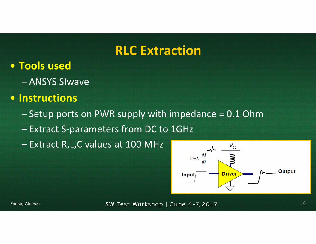
RLC Extraction• Tools used
– ANSYS SIwave
• Instructions
– Setup ports on PWR supply with impedance = 0.1 Ohm
– Extract S-parameters from DC to 1GHz
– Extract R,L,C values at 100 MHz
Pankaj Ahirwar 16

Compute RLGC for a PS
DC resistance can be estimated at 0 HzL,C can be estimated @ 100 MHz
Pankaj Ahirwar 17

Decoupling Capacitor Distance Estimation• Determine if location of decap mounting is close enough to DUT
• Determine loop-inductance of capacitors
Pankaj Ahirwar
Lmnt = Ltrace + Lvia; Ldecap = Lmnt + Lpackage
Using mounting inductance and capacitor package inductance � Resonant Frequency of a decap is determined
���� �1
2�√��� �� ∗ ��� ���
“To be effective Decap needs to be placed within 1/40th of resonant wavelength”
� ��
���� ∗ √��
18

Decoupling Placement for Critical PWR SuppliesDecaps are placed on MLC
Wafer side!
Pankaj Ahirwar
Capacitor Capacitance Value (μF) Resonant Frequency (MHz)(λ/40) (placement distance
to be less than λ/40)
Is placement
distance OK ?
GRM033C81C104KE14D 0.1 38.04 62 mm YES
GRM033C81A105ME05D 1 11.81 202 mm YES
GRM033R71E103ME15 0.01 115.67 20.71 mm YES
19

Decoupling estimates for critical PS/AC target impedance
VDDA target
Pankaj Ahirwar
Estimating Required Decoupling Capacitance
20

MLC
PCB
MLC & PCB combined in same database to get accurate
ac impedance simulations.
PDN Analysis Strategy
Pankaj Ahirwar21

HFSS Analysis of Actual Probe Arrangement
Actual probe layout is simulated in HFSS.This will show any weakness in PDN
Pankaj Ahirwar22

Building Full Channel for PDN (Including Die)
Pankaj Ahirwar23

Correlating Simulations with Measurements• Simulations are prone to errors & can give wrong results…..
– Always know what will be the expected outcome from a simulation
• Measurements are only as accurate as tools/setup/user…….
– VNA/TDR measurements can be tedious and time-consuming
• Correlating Simulation with Measurements is important
– Saves times and resources
– Confidence in simulations and measurements
24Pankaj Ahirwar

S-parameters Measurements, Simulations & Correlation• To measure electrical performance (3 dB bandwidth) of a differential pair on a Probe Card Assembly.
• The selected signals for measurement are (naming convention as per tester channel)
• 3.DIG_CH007
• 3.DIG_CH006
Pankaj Ahirwar25

Measurement Setup
• VNA (HP 8720D 50 MHz to 20 GHz)
• 1250 µm Cascade Microtech probe
• 250 µm Cascade Microtech probe
• Calibration substrate
• Cables & other accessories
• Lab measurements : 50 MHz to 10.5 GHz
26
Pankaj Ahirwar26

PCB Measurements
3.DIG_CH007 3.DIG_CH006
Return_loss (dB) Return_loss (dB)
Insertion_loss (dB) Insertion_loss (dB)
Pankaj Ahirwar27

PCB S-parameter Correlation
Return_loss (dB) Return_loss (dB)
Insertion_loss (dB)
Ins
ert
ion
_lo
ss
(d
B)
Measurement Correlates well with Simulations
Blue: MeasuredRed: Simulated
28

PCB S-parameter Correlation
Re
turn
_lo
ss
(d
B)
Return_loss Measured/Simulated for ERXP
Blue: MeasuredRed: Simulated
Pankaj Ahirwar29

3.DIG_CH007 3.DIG_CH006
Space Transformer Measurements
Return_loss (dB) Return_loss (dB)
Insertion_loss (dB) Insertion_loss (dB)
Pankaj Ahirwar30

3.DIG_CH007 or ERXN
Full Channel Measurements
Return_loss (dB)
Insertion_loss (dB)
Pankaj Ahirwar31

Full Channel Simulations vs Measurements Correlation
Cascading S-parameters for Full Channel Simulations
Probes PCB
Pankaj Ahirwar32
Space Transformer Assembly
POGO Pins

Full Channel Simulations/Measurement Correlation
Ins
ert
ion
_lo
ss
(d
B)
Frequency (Hz)
Excellent correlation is observed between simulated & measured lab data.
Pankaj Ahirwar33

Summary• Early & accurate simulation is key to improve electrical performance of probe cards.
• Accurate simulations results are obtained for controlled impedance structures in probe cards.
• Simulations correlate well with laboratory measurements.
• PCB insertion losses are dominant loss factor (roughly 50% of losses can be attributed to PCB
routes); extra care should be taken during PCB routing.
� Reduce route lengths for critical signals
� PCB stack-up should be optimized to reduce stub lengths on critical signals
� For higher 3dB bandwidths low loss dielectric should be chosen
� SI/PI co-simulation is necessary for designing high performance probe cards.
� Accurate simulations help reduce probe-card design time & this simulation methodology can be
reused on various probe-cards.
Pankaj Ahirwar34

References
• Principles of Power Integrity for PDN Design (1st Edition)
– Larry Smith & Eric Bogatin
– Prentice Hall
• Signal & Power Integrity Simplified (2nd Edition)
– Eric Bogatin
– Prentice Hall
• Board Design Resource Center (www.altera.com)
• Tools
– ANSYS HFSS, SIwave and Keysight ADS & SI/PI pro
35Pankaj Ahirwar