simulation and analysis the performance of 3970 km dwdm
TRANSCRIPT
Abstract—In this paper first we try to analysis the behavior of
the SOAs in the optical networks and then have proposed a numerical simple model to simulate the behavior of the semiconductor optical amplifiers. After that by employing this model as inline amplifier for a DWDM optical system, we have simulated the transmission of 10 channels with bit rate 10 Gb/s up to distance 3970 km with RZ-DPSK modulation format at 20 GHz channel spacing. On the other hand in order to amplify the signal at the transmission link, we have used 73.5km relay span consist of 63km single mode fiber (SMF), 10.5km dispersion compensating fiber (DCF) and a SOA at the end. Our results show that by optimizing the key parameters of the SOA such as the bias current and the input power and furthermore by proper placement of the spans, we can transmit the signal with good amplification and low noise power.
Index Terms—Dense Wavelength Division Multiplexing
(DWDM) Method, Differential Phase Shift Keying (DPSK) Modulation Format, Semiconductor Optical Amplifier (SOA).
I. INTRODUCTION ECENT years, several efforts have been done to improve the performance of the long haul optical communication
networks and increases the total capacity of the system. But up to now the only way to achieve these goals is to utilize dense wavelength division multiplexing (DWDM) technique in the transmission link. On the other hand, performance of such systems is promoted by development of powerful and efficient optical amplifiers, which directly amplify the signal without any conversion to the electrical domain. Semiconductor optical amplifiers (SOAs) as compared to the fiber amplifiers, due to their small size, wideband and flat gain spectrum, low power consumption, ease of integration with other devices and
Manuscript received October 5, 2010 and accepted November 22, 2010.
*Amir Reza Sharifi Pur Shirazi (MSc.) is with the Electrical Engineering Department of the Islamic Azad University - Dariun Branch, Shiraz, Iran, since sep. 2008. (Corresponding author, phone no.: +98-917-737-2204; e-mail: [email protected]).
** Mohsen Kazemian (MSc.) is with the Islamic Azad University - Kerman Branch, Kerman, Iran. (e-mail: [email protected])
*** Masoud Jabbari (PhD.) is with the Islamic Azad University - Marvdasht Branch, Marvdasht, Iran. (e-mail: [email protected])
low cost have became a functional device for optical fibre communication systems [1 and 2]. So these advantages make them so suitable to use as inline amplifier for bidirectional optical systems. Thus by making precise control on the amplifier performance, we can use SOAs as inline amplifier for single and multichannel transmission links. But one of the most important challenges in the way to develop these systems is to optimize the performance of the amplifier due to the dependence of the system performance on the behaviour of the amplifier and placement of the spans along the transmission link and up to now several efforts have been done for optimizing and employing the SOAs in DWDM transmission links [1-8]. In these efforts, the return to zero differential phase shift keying (RZ-DPSK) modulation format has attracted much attention, due to the constant signal power in this format. So in this paper first we have tried to optimize the semiconductor optical amplifiers to increase the transmission relay distance at bit rate 10 Gb/s for DWDM transmission link and then proposed an optimized span scheme to transmit signal toward long haul distances and finally we will show the optimum performance of the proposed amplifier model and the optimized span scheme.
II. PRINCIPLE OPERATION OF SOA In a mathematical manner, first we assume that the input
signal is a continues wave laser (CW) or a pulse laser with pulse width larger than the carrier lifetime. Furthermore in order to simulate and analysis the performance of the semiconductor optical amplifiers in the communication systems, we have to calculate the equation that governs the rate of carriers' population in the active region. When the light is injected to the amplifier medium, some changes will occur in the carrier and photon populations in the active region, indeed we can describe these changes by the variations of the rate equation. So we start the analysis by the material gain coefficient (gm) which is dependent on the carrier density as [1]:
( )tgm NNg −= α (1)
Where N is the carrier density and Nt denotes the carrier density at transparency. The net gain coefficient (gT) which also depends on gm is defined as [1]:
Simulation and Analysis the Performance of 3970 Km DWDM Transmission Link Employing
Optimized Semiconductor Optical Amplifiers Amir R. Sharifi Pur Shirazi, Islamic Azad University - Dariun Branch, Iran *
Mohsen Kazemian, Islamic Azad University - Kerman Branch, Iran ** Masoud Jabbari, Islamic Azad University - Marvdasht Branch, Iran ***
R
Page 155 /183
( ) pm.T
α−Γ= gg (2)
Here αp is the internal waveguide scattering losses (material loss) and Γ is the confinement factor. Finally the amplification factor of the optical wave at the distance z from the input facet of the amplifier is (large signal amplifier gain) [9]:
( ) ( )zgzG .exp
T= (3)
Therefore the rate equation that governs the carrier
population rate in the active region is defined as [1, 2, 9]:
( )fhV
gLePg
NRVqI
dtdN
g
..
1....
.T
T
inm−
Γ
−−= (4)
Where I is the Bias current, q is the electron charge, V is the
active volume, Γ is the confinement factor, L is the length of the amplifier, h is the Plank's constant, f is the optical frequency and R(N) is the recombination rate which is defined as [2]:
( ) 3
aug2
radnr NCNBNANR ++= (5)
Here Anr is the non-radiative recombination coefficient due to the traps and defects in the semiconductor material. Brad is the radiative bimolecular recombination coefficient and Caug is the auger recombination coefficient [2]. So by determining the amplification factor (G) from the above analysis, we can define the amplified spontaneous emission noise power (ASE) at the output of the amplifier as [3]:
( ) ospASE 1 hfBGNP −= (6)
Where Bo is the optical bandwidth of the amplifier and Nsp is the spontaneous emission factor, which defines as [1]:
tsp NN
NN−
= (7)
Which also known as the population inversion factor. The ASE noise power is the most important noise sources in the SOA which is due to the spontaneous emission of the electrons from the conductance band to the valance band. From the above analysis it is obvious that for the low bias current of the SOA with increase in the input power, even if the ASE noise power and the noise figure are quite low, amplification factor will extremely decreases which would increases the crosstalk in the multi channel transmission links as explained in [8]. So we should make a precise control on the bias current and the input power of the amplifier to adjust the gain and the noise of the amplifier in an acceptable value.
III. SOA SIMULATION In order to perform our work, we have assumed a GaInAsP
travelling wave semiconductor optical amplifier (TW-SOA) with negligible residual facet reflectivity (less than 10-4) as the
desired amplifier. So the light will only passes through the forward direction in the amplifier medium and thus no reflections are made [2]. Thus an optical waveguide has been formed within the p/n junction of the laser diode [9]. in order to simulate the behaviour of the amplifier, we have utilized the finite differences method using MATLABTM simulation to solve the rate equation and then the others. So in Table I. we have shown the optimized parameters used in the simulations.
TABLE I.
PARAMETERS USED FOR SIMULATION
Value Parameter Symbol
400 mA Bias Current I
650 µm Length of the Amplifier L
3 µm Active Layer Width w
0.2 µm Active Layer Thickness d
0.3 Optical Confinement Factor Γ
1.1 × 1018 cm-3 Transparency Carrier Density Nt
2.5× 10⁻¹⁶ cm2 Differential Gain αg
40 nm Optical Bandwidth Bo
30 cm-1 Material Loss αp
3 dB Input Output Coupling Efficiency αint
5 × 10⁸ s-1 Non-Radiative Recombination Factor Anr
5 × 10⁻¹⁰ cm3/s Radiative Recombination Factor Brad
1 × 10-28 cm6/s Auger Recombination Factor Caug
But here we should mention that some of these parameters are chosen from [12] which have been experimentally measured and derived. Then we have done the simulations for many variable parameters and optimized the non-experimental parameters such as the length of the amplifier and the bias current and then optimized and employ these parameters in the simulations. Thus all required parameters are listed below in the table.
IV. ANALYSIS THE RESULTS OF THE SOA SIMULATIONS In order to measure the response of the amplifier, we have
to employ the simulated model to calculate the key parameters of the SOA and then analysis the results. But first of all in order to verify the validity of the model we have tested our model with the parameters shown in [8, 9 and 12] and have obtained the same results. After that we have measured the performance of the SOA inline model with the parameters shown in Table I. As shown in Fig. 1. the first step is to calculate the variations of the gain of the amplifier versus the input power. As it is obvious, with increase in the bias current, the amplification factor increases but as the input power increases the amplification factor goes on decreasing, which
Page 156 /183
also was expected from the mathematical analysis.
-20 -15 -10 -5 0 5 10 15 20-10
-5
0
5
10
15
20
25
30
Input Power : Pin (dBm)
Ampl
ifica
tion
Fact
or :
G (d
B)
I = 200 mAI = 400 mAI = 600 mA
Amplification Factor vs. Input Power
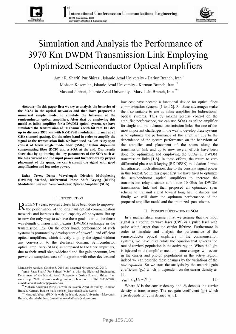
Fig. 1. Amplification factor varies with the signal input power for different bias currents.
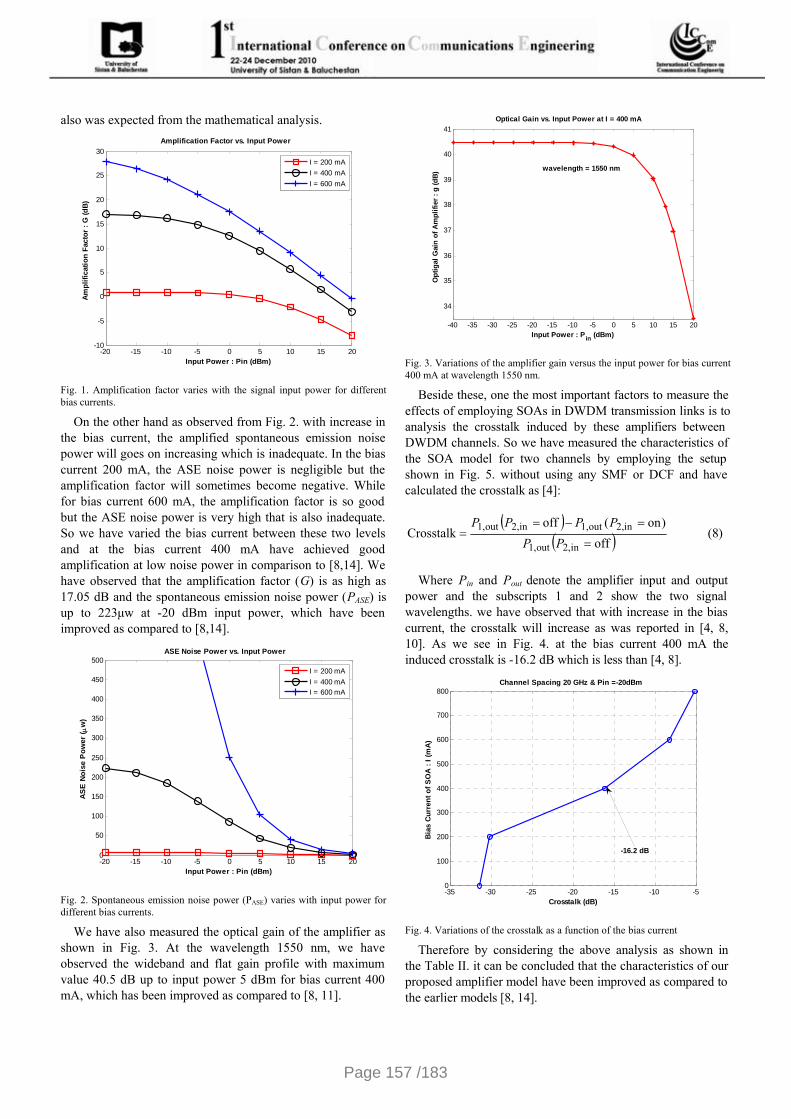
On the other hand as observed from Fig. 2. with increase in the bias current, the amplified spontaneous emission noise power will goes on increasing which is inadequate. In the bias current 200 mA, the ASE noise power is negligible but the amplification factor will sometimes become negative. While for bias current 600 mA, the amplification factor is so good but the ASE noise power is very high that is also inadequate. So we have varied the bias current between these two levels and at the bias current 400 mA have achieved good amplification at low noise power in comparison to [8,14]. We have observed that the amplification factor (G) is as high as 17.05 dB and the spontaneous emission noise power (PASE) is up to 223µw at -20 dBm input power, which have been improved as compared to [8,14].
-20 -15 -10 -5 0 5 10 15 200
50
100
150
200
250
300
350
400
450
500
Input Power : Pin (dBm)
ASE
Noi
se P
ower
( µw
)
I = 200 mAI = 400 mAI = 600 mA
ASE Noise Power vs. Input Power
Fig. 2. Spontaneous emission noise power (PASE) varies with input power for different bias currents.
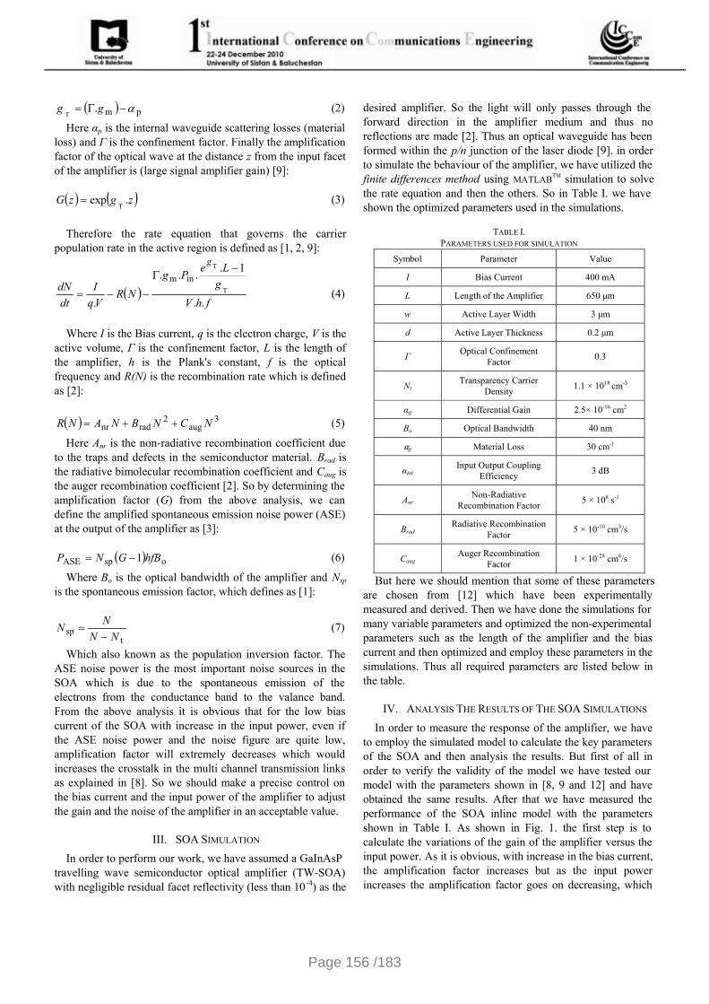
We have also measured the optical gain of the amplifier as shown in Fig. 3. At the wavelength 1550 nm, we have observed the wideband and flat gain profile with maximum value 40.5 dB up to input power 5 dBm for bias current 400 mA, which has been improved as compared to [8, 11].
-40 -35 -30 -25 -20 -15 -10 -5 0 5 10 15 20
34
35
36
37
38
39
40
41
Input Power : Pin (dBm)
Opt
igal
Gai
n of
Am
plifi
er :
g (d
B)
wavelength = 1550 nm
Optical Gain vs. Input Power at I = 400 mA
Fig. 3. Variations of the amplifier gain versus the input power for bias current 400 mA at wavelength 1550 nm.
Beside these, one the most important factors to measure the effects of employing SOAs in DWDM transmission links is to analysis the crosstalk induced by these amplifiers between DWDM channels. So we have measured the characteristics of the SOA model for two channels by employing the setup shown in Fig. 5. without using any SMF or DCF and have calculated the crosstalk as [4]:
( )( )off
)on(offCrosstalk
2,inout1,
2,inout1,2,inout1,
=
=−==
PPPPPP
(8)
Where Pin and Pout denote the amplifier input and output
power and the subscripts 1 and 2 show the two signal wavelengths. we have observed that with increase in the bias current, the crosstalk will increase as was reported in [4, 8, 10]. As we see in Fig. 4. at the bias current 400 mA the induced crosstalk is -16.2 dB which is less than [4, 8].
-35 -30 -25 -20 -15 -10 -50
100
200
300
400
500
600
700
800
Crosstalk (dB)
Bias
Cur
rent
of S
OA
: I (m
A)
-16.2 dB
Channel Spacing 20 GHz & Pin =-20dBm
Fig. 4. Variations of the crosstalk as a function of the bias current
Therefore by considering the above analysis as shown in the Table II. it can be concluded that the characteristics of our proposed amplifier model have been improved as compared to the earlier models [8, 14].
Page 157 /183
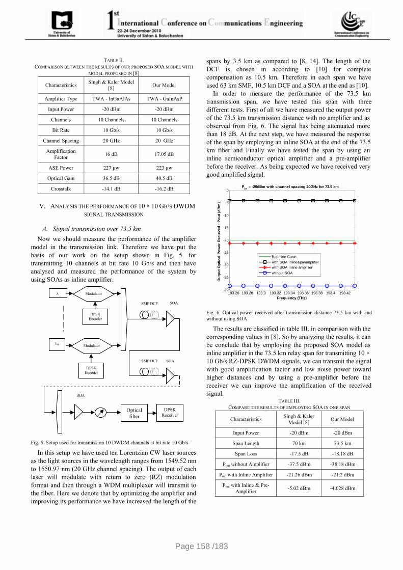
TABLE II.
COMPARISON BETWEEN THE RESULTS OF OUR PROPOSED SOA MODEL WITH MODEL PROPOSED IN [8]
Characteristics Singh & Kaler Model [8] Our Model
Amplifier Type TWA - InGaAlAs TWA - GaInAsP
Input Power -20 dBm -20 dBm
Channels 10 Channels 10 Channels
Bit Rate 10 Gb/s 10 Gb/s
Channel Spacing 20 GHz 20 GHz
Amplification Factor 16 dB 17.05 dB
ASE Power 227 µw 223 µw
Optical Gain 36.5 dB 40.5 dB
Crosstalk -14.1 dB -16.2 dB
V. ANALYSIS THE PERFORMANCE OF 10 × 10 GB/S DWDM SIGNAL TRANSMISSION
A. Signal transmission over 73.5 km Now we should measure the performance of the amplifier
model in the transmission link. Therefore we have put the basis of our work on the setup shown in Fig. 5. for transmitting 10 channels at bit rate 10 Gb/s and then have analysed and measured the performance of the system by using SOAs as inline amplifier.
Fig. 5. Setup used for transmission 10 DWDM channels at bit rate 10 Gb/s
In this setup we have used ten Lorentzian CW laser sources as the light sources in the wavelength ranges from 1549.52 nm to 1550.97 nm (20 GHz channel spacing). The output of each laser will modulate with return to zero (RZ) modulation format and then through a WDM multiplexer will transmit to the fiber. Here we denote that by optimizing the amplifier and improving its performance we have increased the length of the
spans by 3.5 km as compared to [8, 14]. The length of the DCF is chosen in according to [10] for complete compensation as 10.5 km. Therefore in each span we have used 63 km SMF, 10.5 km DCF and a SOA at the end as [10].
In order to measure the performance of the 73.5 km transmission span, we have tested this span with three different tests. First of all we have measured the output power of the 73.5 km transmission distance with no amplifier and as observed from Fig. 6. The signal has being attenuated more than 18 dB. At the next step, we have measured the response of the span by employing an inline SOA at the end of the 73.5 km fiber and Finally we have tested the span by using an inline semiconductor optical amplifier and a pre-amplifier before the receiver. As being expected we have received very good amplified signal.
193.26 193.28 193.3 193.32 193.34 193.36 193.38 193.4 193.42-40
-35
-30
-25
-20
-15
-10
-5
0
Frequency (THz)
Out
put O
ptic
al P
ower
Rec
ieve
d : P
out (
dBm
)
Baseline Curvewith SOA inline&preamplifierwith SOA inline amplifierwithout SOA
Pin = -20dBm with channel spacing 20GHz for 73.5 km
Fig. 6. Optical power received after transmission distance 73.5 km with and without using SOA
The results are classified in table III. in comparison with the corresponding values in [8]. So by analyzing the results, it can be conclude that by employing the proposed SOA model as inline amplifier in the 73.5 km relay span for transmitting 10 × 10 Gb/s RZ-DPSK DWDM signals, we can transmit the signal with good amplification factor and low noise power toward higher distances and by using a pre-amplifier before the receiver we can improve the amplification of the received signal.
TABLE III. COMPARE THE RESULTS OF EMPLOYING SOA IN ONE SPAN
Characteristics Singh & Kaler Model [8] Our Model
Input Power -20 dBm -20 dBm
Span Length 70 km 73.5 km
Span Loss -17.5 dB -18.18 dB
Pout without Amplifier -37.5 dBm -38.18 dBm
Pout with Inline Amplifier -21.26 dBm -21.2 dBm
Pout with Inline & Pre-Amplifier -5.02 dBm -4.028 dBm
λ1 Modulator
DPSK Encoder
Optical filter
DPSK Receiver
λ10 Modulator
DPSK Encoder
| | | |
SMF DCF
SMF DCF
SOA
SOA
SOA
Page 158 /183

B. DWDM signal transmission up to 3970 km at bit rate 100 Gb/s Up to now various schemes have been proposed to transmit
DWDM signals toward long haul distances which have categorized in two branches: the conventional span schemes and the equal span schemes [8]. But beside these two schemes we can utilize another one by changing the placement of the spans, known as improved or optimized span scheme. So we have measured the transmission of DWDM signal up to distance 3970 km by employing conventional, equal and optimized span schemes and then will show the optimum performance of the optimized span scheme. In Fig. 7a. the schematic of the conventional span scheme has been shown. As observed from the figure we have to use 54 spans and finally 1 km SMF at the end of the transmission link. In Fig. 7b. the schematic of the equal span scheme has been shown. In this scheme we have divided the transmission link into 3 equal distances, each consist of 18 spans and a SOA after each to amplify the signal. On the other hand as we see in the Fig. 7c. in the improved span scheme, instead of the equal placement of the spans we can change this placement and achieve better performance. So by using the iterations and error method we have chosen this placement to improve the spans: 20, 15, 10 and 9.
In the conventional span scheme because of the continues attenuation of the transmitted signal along the transmission link, we will observe a very extremely power drops at the end of the transmission distance as [8]. So the conventional span scheme would not be proper for the long haul transmission distances. On the other hand, the equal span scheme shows a better performance for the long haul transmission links. But in this scheme we will again observe that the received power is much lower than the input power. On the other hand one of the greatest disadvantages of the equal span scheme is that the ASE power here is much higher than the conventional scheme [8]. This is due to accumulative addition of the emission noise along the transmission link because of more SOAs we have used. So it is required to propose a scheme that represents a good performance. In this scheme the input power of each SOA should be less than the saturation power to perform in a linear regime [8]. Thus we would receive better performance as shown in Table IV.
TABLE IV.
RESULTS OF DWDM TRANSMISSION FOR 3970 KM Characteristics Value
System Input power -20 dBm
Output Power of the Conventional Span Scheme -68.96 dBm
Output Power of the Equal Span Scheme -34.9 dBm
Output Power of the Optimized Span Scheme -18.03 dBm
Because of setting the input power of each SOA below the saturation value, the accumulative noise would be less than
the equal span scheme but higher than the conventional placement. So we have:
eq.ASEopt.ASEconv.ASE PPP << (9)
Fig. 7. a) Conventional span scheme up to distance 3970 km. b) Equal span scheme. c) Optimized span scheme.
SOA
SOA
SOA
SOA
SOA
a)
b)
SMF DCF
SOA
10 × 10 GB/s RZ-DPSK
Output Signal
10 × 10 GB/s RZ-DPSK
Input Signal
54 Spans
SMF DCF
10 × 10 GB/s RZ-DPSK
Output Signal
18 SpansSOA
SMF DCF
SOA
SMF DCF
SOA
18 Spans
18 Spans
c)
SMF DCF
10 × 10 GB/s RZ-DPSK
Output Signal
10 × 10 GB/s RZ-DPSK
Input Signal 20 SpansSOA
SMF DCF
SOA
SMF DCF
SOA
15 Spans
9 Spans
SMF DCF
SO 10 Spans
10 × 10 GB/s RZ-DPSK
Input Signal
Page 159 /183
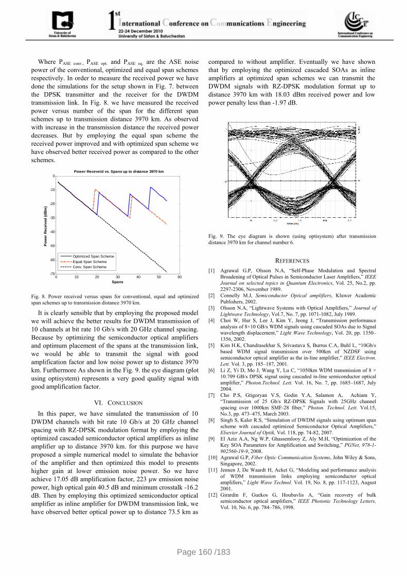
Where PASE conv., PASE opt. and PASE eq. are the ASE noise power of the conventional, optimized and equal span schemes respectively. In order to measure the received power we have done the simulations for the setup shown in Fig. 7. between the DPSK transmitter and the receiver for the DWDM transmission link. In Fig. 8. we have measured the received power versus number of the span for the different span schemes up to transmission distance 3970 km. As observed with increase in the transmission distance the received power decreases. But by employing the equal span scheme the received power improved and with optimized span scheme we have observed better received power as compared to the other schemes.
0 10 20 30 40 50 60-70
-60
-50
-40
-30
-20
-10
0
Spans
Pow
er R
ecei
ved
(dBm
)
Optimized Span SchemeEqual Span SchemeConv. Span Scheme
Power Receveid vs. Spans up to distance 3970 km
Fig. 8. Power received versus spans for conventional, equal and optimized span schemes up to transmission distance 3970 km.
It is clearly sensible that by employing the proposed model we will achieve the better results for DWDM transmission of 10 channels at bit rate 10 Gb/s with 20 GHz channel spacing. Because by optimizing the semiconductor optical amplifiers and optimum placement of the spans at the transmission link, we would be able to transmit the signal with good amplification factor and low noise power up to distance 3970 km. Furthermore As shown in the Fig. 9. the eye diagram (plot using optisystem) represents a very good quality signal with good amplification factor.
VI. CONCLUSION In this paper, we have simulated the transmission of 10
DWDM channels with bit rate 10 Gb/s at 20 GHz channel spacing with RZ-DPSK modulation format by employing the optimized cascaded semiconductor optical amplifiers as inline amplifier up to distance 3970 km. for this purpose we have proposed a simple numerical model to simulate the behavior of the amplifier and then optimized this model to presents higher gain at lower emission noise power. So we have achieve 17.05 dB amplification factor, 223 µw emission noise power, high optical gain 40.5 dB and minimum crosstalk -16.2 dB. Then by employing this optimized semiconductor optical amplifier as inline amplifier for DWDM transmission link, we have observed better optical power up to distance 73.5 km as
compared to without amplifier. Eventually we have shown that by employing the optimized cascaded SOAs as inline amplifiers at optimized span schemes we can transmit the DWDM signals with RZ-DPSK modulation format up to distance 3970 km with 18.03 dBm received power and low power penalty less than -1.97 dB.
Fig. 9. The eye diagram is shown (using optisystem) after transmission distance 3970 km for channel number 6.
REFERENCES [1] Agrawal G.P, Olsson N.A, “Self-Phase Modulation and Spectral
Broadening of Optical Pulses in Semiconductor Laser Amplifiers,” IEEE Journal on selected topics in Quantum Electronics, Vol. 25, No.2, pp. 2297-2306, November 1989.
[2] Connelly M.J, Semiconductor Optical amplifiers, Kluwer Academic Publishers, 2002.
[3] Olsson N.A, “Lightwave Systems with Optical Amplifiers,” Journal of Lightwave Technology, Vol.7, No. 7, pp. 1071-1082, July 1989.
[4] Choi W, Hur S, Lee J, Kim Y, Jeong J, “Transmission performance analysis of 8×10 GB/s WDM signals using cascaded SOAs due to Signal wavelength displacement,” Light Wave Technology, Vol. 20, pp. 1350–1356, 2002.
[5] Kim H.K, Chandrasekhar S, Srivastava S, Burrus C.A, Buhl L, “10Gb/s based WDM signal transmission over 500km of NZDSF using semiconductor optical amplifier as the in-line amplifier,” IEEE Electron. Lett. Vol. 3, pp. 185–187, 2001.
[6] Li Z, Yi D, Mo J, Wang Y, Lu C, “1050km WDM transmission of 8 × 10.709 GB/s DPSK signal using cascaded in-line semiconductor optical amplifier,” Photon.Technol. Lett. Vol. 16, No. 7, pp. 1685–1687, July 2004.
[7] Cho P.S, Gtigoryan V.S, Godin Y.A, Salamon A, Achiam Y, “Transmission of 25 Gb/s RZ-DPSK Signals with 25GHz channel spacing over 1000km SMF-28 fiber,” Photon. Technol. Lett. Vol.15, No.3, pp. 473–475, March 2003.
[8] Singh S, Kaler R.S, “Simulation of DWDM signals using optimum span scheme with cascaded optimized Semiconductor Optical Amplifiers,” Elsevier Journal of Optik, Vol. 118, pp. 74-82, 2007.
[9] El Aziz A.A, Ng W.P, Ghassemlooy Z, Aly M.H, “Optimization of the Key SOA Parameters for Amplification and Switching,” PGNet, 978-1-902560-19-9, 2008.
[10] Agrawal G.P, Fiber Optic Communication Systems, John Wiley & Sons, Singapore, 2002.
[11] Jennen J, De Waardt H, Acket G, “Modeling and performance analysis of WDM transmission links employing semiconductor optical amplifiers,” Light Wave Technol. Vol. 19, No. 8, pp. 117-1123, August 2001.
[12] Girardin F, Guekos G, Houbavlis A, “Gain recovery of bulk semiconductor optical amplifiers,” IEEE Photonic Technology Letters, Vol. 10, No. 6, pp. 784–786, 1998.
Page 160 /183