simulation examples - ntuausers.ntua.gr/manias/pspice1-3.pdf · pspice user's guide 61 2...
TRANSCRIPT

PSpice User's Guide 61
2
Simulation examples
Chapter overview
The examples in this chapter provide an introduction to themethods and tools for creating circuit designs, runningsimulations, and analyzing simulation results. All analyses areperformed on the same example circuit to clearly illustrateanalysis setup, simulation, and result-analysis procedures foreach analysis type.
This chapter includes the following sections:
Example circuit creation on page 62
Performing a bias point analysis on page 69
DC sweep analysis on page 72
Transient analysis on page 79
AC sweep analysis on page 84
Parametric analysis on page 89
Performance analysis on page 97
Chapter 2 Simulation examples Product Version 10.0
62 PSpice User's Guide
Example circuit creation
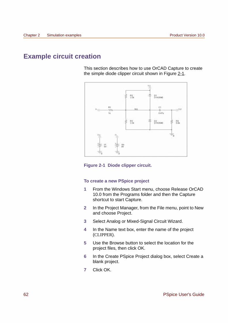
This section describes how to use OrCAD Capture to createthe simple diode clipper circuit shown in Figure 2-1.
Figure 2-1 Diode clipper circuit.
To create a new PSpice project
1 From the Windows Start menu, choose Release OrCAD10.0 from the Programs folder and then the Captureshortcut to start Capture.
2 In the Project Manager, from the File menu, point to Newand choose Project.
3 Select Analog or Mixed-Signal Circuit Wizard.
4 In the Name text box, enter the name of the project(CLIPPER).
5 Use the Browse button to select the location for theproject files, then click OK.
6 In the Create PSpice Project dialog box, select Create ablank project.
7 Click OK.

Product Version 10.0 Chapter overview
PSpice User's Guide 63
No special libraries need to be configured at this time. Anew page will be displayed in Capture and the newproject will be configured in the Project Manager.
To place the voltage sources
1 In Capture, switch to the schematic page editor.
2 From the Place menu, choose Part to display the PlacePart dialog box.
3 Add the library for the parts you need to place:
a. Click the Add Library button.
b. Select SOURCE.OLB (from the PSpice library) andclick Open.
Note: There are two sets of library files supplied withCapture and PSpice. The standard schematic partlibraries are found in the directory\TOOLS\CAPTURE\LIBRARY. The part libraries that aredesigned for simulation with PSpice are found in thesub-directory \TOOLS\CAPTURE\LIBRARY\PSPICE. Inorder to have access to specific parts, you must firstconfigure the library in Capture using the Add Libraryfunction.
4 In the Part text box, type VDC.
5 Click OK.
6 Move the pointer to the correct position on the schematicpage (see Figure 2-1) and click to place the first part.
7 Move the cursor and click again to place the second part.
8 Right-click and choose End Mode to stop placing parts.
To place the diodes
1 From the Place menu, choose Part to display the PlacePart dialog box.
2 Add the library for the parts you need to place:
Chapter 2 Simulation examples Product Version 10.0
64 PSpice User's Guide
a. Click the Add Library button.
b. Select DIODE.OLB (from the PSpice library) andclick Open.
3 In the Part text box, type D1N39 to display a list of diodes.
When placing parts:
Leave space to connect the parts with wires.
You will change part names and values that do notmatch those shown in Figure 2-1 later in this section.
4 Select D1N3940 from the Part List and click OK.
5 Press R to rotate the diode to the correct orientation.
6 Click to place the first diode (D1), then click to place thesecond diode (D2).
7 Right-click and choose End Mode to stop placing parts.
To move the text associated with the diodes (or any otherobject)
1 Click the text to select it, then drag the text to a newlocation.
To place the other parts
1 From the Place menu, choose Part to display the PlacePart dialog box.
2 Add the library for the parts you need to place:
a. Click the Add Library button.
b. Select ANALOG.OLB (from the PSpice library) andclick Open.
3 Follow similar steps as described for the diodes to placethe parts listed below, according to Figure 2-1 onpage 62. The part names you need to type in the Partname text box of the Place Part dialog box are shown inparentheses:
resistors (R)
Product Version 10.0 Chapter overview
PSpice User's Guide 65
capacitor (C)
4 To place the off-page connector parts(OFFPAGELEFT-R), click the Place Off-Page Connectorbutton on the tool palette.
5 Add the library for the parts you need to place:
a. Click the Add Library button.
b. Select CAPSYM.OLB (from the Capture library) andclick Open.
6 Place the off-page connector parts according toFigure 2-1 on page 62.
Note: To rotate the part so the arrows are pointing in thecorrect direction, place the part, select it, then press Rone or more times to rotate the part to the desiredorientation.
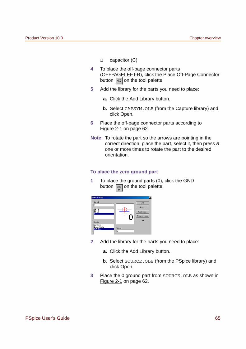
To place the zero ground part
1 To place the ground parts (0), click the GNDbutton on the tool palette.
2 Add the library for the parts you need to place:
a. Click the Add Library button.
b. Select SOURCE.OLB (from the PSpice library) andclick Open.
3 Place the 0 ground part from SOURCE.OLB as shown inFigure 2-1 on page 62.

Chapter 2 Simulation examples Product Version 10.0
66 PSpice User's Guide
Important
You must use the 0 (zero) ground part from theSOURCE.OLB part library. You can use any otherground part only if you change its name to 0 (zero).
To connect the parts
1 From the Place menu, choose Wire to begin wiring parts.
The pointer changes to a crosshair.
2 Click the connection point (the very end) of the pin on theoff-page connector at the input of the circuit.
3 Click the nearest connection point of the input resistor R1.
To stop wiring, right-click and choose End Wire. Thepointer changes to the default arrow.
Clicking on any valid connection point ends a wire. A validconnection point is shown as a box (see Figure 2-2).
If you make a mistake when placing or connectingcomponents:
From the Edit menu, choose Undo, or click .
4 Connect the other end of R1 to the output capacitor.
5 Connect the diodes to each other and to the wire betweenthem:
a. Click the connection point of the cathode for thelower diode.
b. Move the cursor straight up and click the wirebetween the diodes. The wire ends, and the junctionof the wire segments becomes visible.
Figure 2-2 Connection points.

Product Version 10.0 Chapter overview
PSpice User's Guide 67
c. Click again on the junction to continue wiring.
d. Click the end of the upper diode’s anode pin.
6 Continue connecting parts until the circuit is wired asshown in Figure 2-1 on page 62.
To assign names (labels) to the nets
1 From the Place menu, choose Net Alias to display thePlace Net Alias dialog box.
2 In the Name text box, type Mid.
3 Click OK.
4 Place the net alias on any segment of the wire thatconnects R1, R2, R3, the diodes, and the capacitor. Thelower left corner of the net alias must touch the wire.
5 Right-click and choose End Mode to quit the Net Aliasfunction.
To assign names (labels) to the off-page connectors
Label the off-page connectors as shown in Figure 2-1 onpage 62.
1 Double-click the name of an off-page connector to displaythe Display Properties dialog box.
2 In the Name text box, type the new name.
3 Click OK.
4 Select and relocate the new name as desired.
To assign names to the parts
1 Double-click the second VDC part to display the Partsspreadsheet.
2 Click in the first cell under the Reference column.
3 Type in the new name Vin.

Chapter 2 Simulation examples Product Version 10.0
68 PSpice User's Guide
4 Click Apply to update the changes to the part, then closethe spreadsheet.
5 Continue naming the remaining parts until yourschematic looks like Figure 2-1 on page 62.
Tip
A more efficient way to change the names, valuesand other properties of several parts in your designis to use the Property Editor, as follows:
a. Select all of the parts to be modified by pressing Ctrland clicking each part.
b. From the Edit menu, choose Properties.
The Parts Spreadsheet appears.
Change the entries in as many of the cells as needed,and then click Apply to update all of the changes at once.
To change the values of the parts
1 Double-click the voltage label (0V) on V1 to display theDisplay Properties dialog box.
2 In the Value text box, type 5V.
3 Click OK.
4 Continue changing the Part Value properties of the partsuntil all the parts are defined as in Figure 2-1 on page 62.
Your schematic page should now have the same parts,wiring, labels, and properties as Figure 2-1 on page 62.
To save your design
1 From the File menu, choose Save.

Product Version 10.0 Running PSpice
PSpice User's Guide 69
Finding out more about setting up your design
About setting up a design for simulation
For a checklist of all of the things you need to do to set up yourdesign for simulation, and how to avoid common problems,see Chapter 3, “Preparing a design for simulation.”
Running PSpice
When you perform a simulation, PSpice generates an outputfile (*.OUT).
While PSpice is running, the progress of the simulationappears and is updated in the PSpice simulation outputwindow (see Figure 2-3).
Figure 2-3 PSpice simulation output window.
You can set up a simulation profile to run one analysis at atime. To run multiple analyses (for example, both DC sweepand transient analyses), set up a batch simulation. For moreinformation, see Chapter 8, “Setting up analyses and startingsimulation.”
Performing a bias point analysis
To set up a bias point analysis in Capture
1 In Capture, switch to CLIPPER.OPJ in the schematicpage editor.

Chapter 2 Simulation examples Product Version 10.0
70 PSpice User's Guide
2 From the PSpice menu, choose New Simulation Profile todisplay the New Simulation dialog box.
3 In the Name text box, type Bias.
4 From the Inherit From list, select None, then click Create.
The Simulation Settings dialog box appears.
The root schematic listed is the schematic pageassociated with the simulation profile you are creating.
5 From the Analysis type list, select Bias Point.
6 Click OK to close the Simulation Settings dialog box.
To simulate the circuit from within Capture
1 From the PSpice menu, choose Run.
PSpice simulates the circuit and calculates the bias pointinformation.
Note: Because waveform data is not calculated during a biaspoint analysis, you will not see any plots displayed inthe Probe window for this simulation. To find out how toview the results of this simulation, see Using thesimulation output file below.

Product Version 10.0 Running PSpice
PSpice User's Guide 71
Using the simulation output file
The simulation output file acts as an audit trail of thesimulation. This file optionally echoes the contents of thecircuit file as well as the results of the bias point calculation. Ifthere are any syntax errors in the netlist declarations orsimulation commands, or anomalies while performing thecalculation, PSpice writes error or warning messages to theoutput file.
To view the simulation output file
1 In PSpice, from the View menu, choose Output File.
Figure 2-4 shows the results of the bias point calculationas written in the simulation output file.
2 When finished, close the window.
PSpice measures the current through a two-terminal deviceinto the first terminal and out of the second terminal. Forvoltage sources, current is measured from the positiveterminal to the negative terminal; this is opposite to thepositive current flow convention and results in a negative valuein the output file.
Figure 2-4 Simulation output file.

Chapter 2 Simulation examples Product Version 10.0
72 PSpice User's Guide
Finding out more about bias point calculations
DC sweep analysis
You can visually verify the DC response of the clipper byperforming a DC sweep of the input voltage source anddisplaying the waveform results in the Probe window inPSpice. This example sets up DC sweep analysis parametersto sweep Vin from -10 to 15 volts in 1 volt increments.
Setting up and running a DC sweep analysis
To set up and run a DC sweep analysis
1 In Capture, from the PSpice menu, chooseNew Simulation Profile.
The New Simulation dialog box appears.
2 In the Name text box, type DC Sweep.
3 From the Inherit From list, select Schematic1-Bias, thenclick Create.
The Simulation Settings dialog box appears.
4 Click the Analysis tab.
5 From the Analysis type list, select DC Sweep and enterthe values shown in Figure 2-5.
Note: The default settings for DC Sweep simulation areVoltage source as the swept variable type and Linear asthe sweep type. To use a different swept variable type orsweep type, choose different options under Sweep
To find out more aboutthis...
See this...
Bias point calculations Bias point on page 409

Product Version 10.0 DC sweep analysis
PSpice User's Guide 73
variable and Sweep type.
6 Click OK to close the Simulation Settings dialog box.
7 From the File menu, choose Save.
8 From the PSpice menu, choose Run to run the analysis.
Figure 2-5 DC sweep analysis settings.

Chapter 2 Simulation examples Product Version 10.0
74 PSpice User's Guide
Displaying DC analysis results
Probe windows can appear during or after the simulation isfinished.
To plot voltages at nets In and Mid
1 From PSpice’s Trace menu, choose Add Trace.
2 In the Add Traces dialog box, select V(In) and V(Mid).
3 Click OK.
To display a trace using a marker
1 From Capture’s PSpice menu, point to Markers andchoose Voltage Level.
Figure 2-7 Probe window.
Product Version 10.0 DC sweep analysis
PSpice User's Guide 75
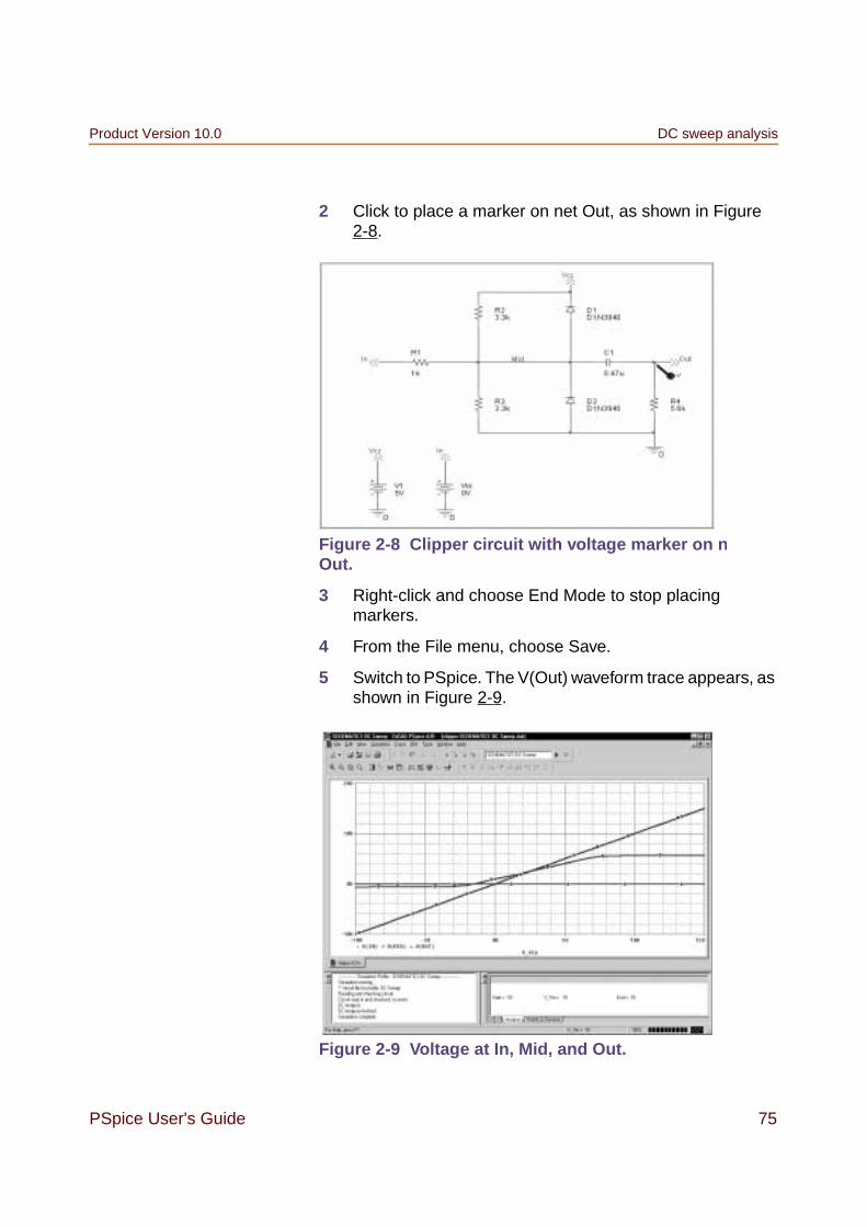
2 Click to place a marker on net Out, as shown in Figure2-8.
3 Right-click and choose End Mode to stop placingmarkers.
4 From the File menu, choose Save.
5 Switch to PSpice. The V(Out) waveform trace appears, asshown in Figure 2-9.
Figure 2-8 Clipper circuit with voltage marker on nOut.
Figure 2-9 Voltage at In, Mid, and Out.

Chapter 2 Simulation examples Product Version 10.0
76 PSpice User's Guide
To place cursors on V(In) and V(Mid)
This example uses the cursors feature to view the numericvalues for two traces and the difference between them byplacing a cursor on each trace.
1 From PSpice’s Trace menu, point to Cursor and chooseDisplay.
Two cursors appear for the first trace defined in thelegend below the x-axis—V(In) in this example. TheProbe Cursor window also appears.
2 To display the cursor crosshairs:
a. Position the mouse anywhere inside the Probewindow.
b. Click to display the crosshairs for the first cursor.
c. Right-click to display the crosshairs for the secondcursor.
Table 2-1 Association of cursors with mousebuttons.
In the trace legend, the part for V(In) is outlined in thecrosshair pattern for each cursor, resulting in a dashedline as shown in Figure 2-10.
3 Place the first cursor on the V(In) waveform:
a. Click the portion of the V(In) trace in the proximity of4 volts on the x-axis. The cursor crosshair appears,
cursor 1 left mouse button
cursor 2 right mouse button
Figure 2-10 Trace legend with cursors activated.

Product Version 10.0 DC sweep analysis
PSpice User's Guide 77
and the current X and Y values for the first cursorappear in the cursor window.
b. To fine-tune the cursor location to 4 volts on thex-axis, drag the crosshairs until the x-axis value ofthe A1 cursor in the cursor window is approximately4.0. You can also press Right arrow key and Leftarrow key for tighter control.
Note: Your ability to get as close to 4.0 as possibledepends on screen resolution and window size.
4 Place the second cursor on the V(Mid) waveform:
a. Right-click the trace legend part (diamond) forV(Mid) to associate the second cursor with the Midwaveform. The crosshair pattern for the secondcursor outlines the V(Mid) trace part as shown inFigure 2-11.
b. Right-click the portion on the V(Mid) trace that is inthe proximity of 4 volts on the x-axis. The X and Yvalues for the second cursor appear in the cursorwindow along with the difference (dif) between thetwo cursors’ X and Y values.
c. To fine-tune the location of the second cursor to 4volts on the x-axis, drag the crosshairs until thex-axis value of the A2 cursor in the cursor window isapproximately 4.0. You can also press Shift+Rightarrow key and Shift+Left arrow key for tightercontrol.
Figure 2-11 Trace legend with V(Mid)symbol outlined.
Chapter 2 Simulation examples Product Version 10.0
78 PSpice User's Guide
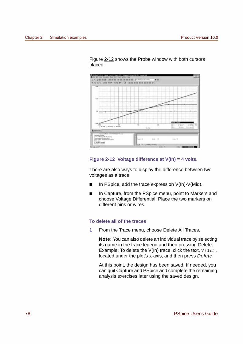
Figure 2-12 shows the Probe window with both cursorsplaced.
Figure 2-12 Voltage difference at V(In) = 4 volts.
There are also ways to display the difference between twovoltages as a trace:
In PSpice, add the trace expression V(In)-V(Mid).
In Capture, from the PSpice menu, point to Markers andchoose Voltage Differential. Place the two markers ondifferent pins or wires.
To delete all of the traces
1 From the Trace menu, choose Delete All Traces.
Note: You can also delete an individual trace by selectingits name in the trace legend and then pressing Delete.Example: To delete the V(In) trace, click the text, V(In),located under the plot’s x-axis, and then press Delete.
At this point, the design has been saved. If needed, youcan quit Capture and PSpice and complete the remaininganalysis exercises later using the saved design.
Product Version 10.0 Transient analysis
PSpice User's Guide 79
Finding out more about DC sweep analysis
Transient analysis
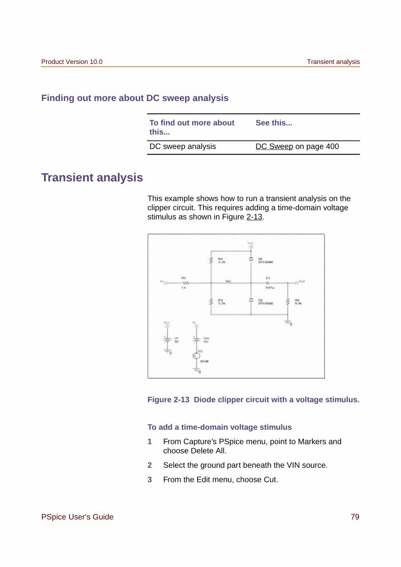
This example shows how to run a transient analysis on theclipper circuit. This requires adding a time-domain voltagestimulus as shown in Figure 2-13.
Figure 2-13 Diode clipper circuit with a voltage stimulus.
To add a time-domain voltage stimulus
1 From Capture’s PSpice menu, point to Markers andchoose Delete All.
2 Select the ground part beneath the VIN source.
3 From the Edit menu, choose Cut.
To find out more aboutthis...
See this...
DC sweep analysis DC Sweep on page 400

Chapter 2 Simulation examples Product Version 10.0
80 PSpice User's Guide
4 Scroll down (or from the View menu, point to Zoom, thenchoose Out).
5 Place a VSTIM part (from the PSpice librarySOURCSTM.OLB) as shown in Figure 2-13.
6 From the Edit menu, choose Paste.
7 Place the ground part under the VSTIM part as shown inFigure 2-13.
8 From the View menu, point to Zoom, then choose All.
9 From the File menu, choose Save to save the design.
To set up the stimulus
Note: The Stimulus Editor is not available inPSpice A/D Basics. If you are usingPSpice A/D Basics, see If you do not have theStimulus Editor on page 81.
1 Select the VSTIM part (V3).
2 From the Edit menu, choose PSpice Stimulus.
The New Stimulus dialog box appears.
3 In the New Stimulus dialog box, type SINE.
4 Click SIN (sinusoidal), then click OK.
5 In the SIN Attributes dialog box, set the first threeproperties as follows:
Offset Voltage = 0Amplitude = 10Frequency = 1kHz
6 Click Apply to view the waveform.

Product Version 10.0 Transient analysis
PSpice User's Guide 81
The Stimulus Editor window should look like Figure 2-14.
7 Click OK.
8 From the File menu, choose Save to save the stimulusinformation. Click Yes to update the schematic.
9 From the File menu, choose Exit to exit the StimulusEditor.
If you do not have the Stimulus Editor
1 Place a VSIN part instead of VSTIM and double-click it.
2 In the Edit Part dialog box, click User Properties.
3 Set values for the VOFF, VAMPL, and FREQ propertiesas defined in step 5. When finished, click OK.
To set up and run the transient analysis
1 From Capture’s PSpice menu, chooseNew Simulation Profile.
The New Simulation dialog box appears.
2 In the Name text box, type Transient.
Figure 2-14 Stimulus Editor window.

Chapter 2 Simulation examples Product Version 10.0
82 PSpice User's Guide
3 From the Inherit From list, select Schematic1-DC Sweep,then click Create.
The Simulation Settings dialog box appears.
4 Click the Analysis tab.
5 From the Analysis list, select Time Domain (Transient)and enter the settings shown in Figure 2-15.
TSTOP = 2ms
Start saving data after = 20ns
6 Click OK to close the Simulation Settings dialog box.
7 From the PSpice menu, choose Run to perform theanalysis.
PSpice uses its own internal time steps for computation.The internal time step is adjusted according to therequirements of the transient analysis as it proceeds.PSpice saves data to the waveform data file for eachinternal time step.
Note: The internal time step is different from the PrintStep value. Print Step controls how often optional textformat data is written to the simulation output file (*.OUT).
To display the input sine wave and clipped wave at V(Out)
1 From PSpice’s Trace menu, choose Add Trace.
2 In the trace list, select V(In) and V(Out) by clicking them.
Figure 2-15 Transientanalysis simulationsettings.
Product Version 10.0 Transient analysis
PSpice User's Guide 83
3 Click OK to display the traces.
4 From the Tools menu, choose Options to display theProbe Options dialog box.
5 In the Use Symbols frame, click Always if it is not alreadyenabled.
6 Click OK.
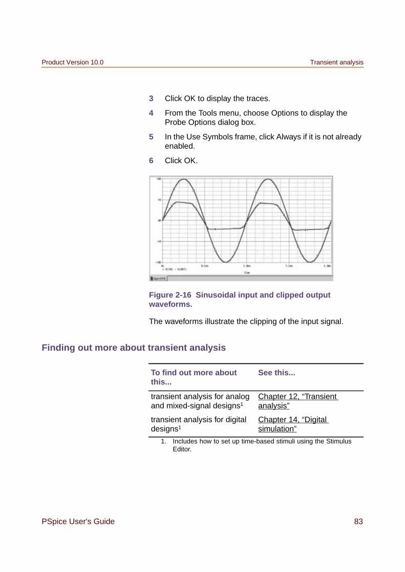
Figure 2-16 Sinusoidal input and clipped outputwaveforms.
The waveforms illustrate the clipping of the input signal.
Finding out more about transient analysis
To find out more aboutthis...
See this...
transient analysis for analogand mixed-signal designs1
1. Includes how to set up time-based stimuli using the StimulusEditor.
Chapter 12, “Transientanalysis”
transient analysis for digitaldesigns1
Chapter 14, “Digitalsimulation”

Chapter 2 Simulation examples Product Version 10.0
84 PSpice User's Guide
AC sweep analysis
The AC sweep analysis in PSpice is a linear (or small signal)frequency domain analysis that can be used to observe thefrequency response of any circuit at its bias point.
Setting up and running an AC sweep analysis
In this example, you will set up the clipper circuit for ACanalysis by adding an AC voltage source for a stimulus signal(see Figure 2-17) and by setting up AC sweep parameters.
Figure 2-17 Clipper circuit with AC stimulus.
To change Vin to include the AC stimulus signal
1 In Capture, open CLIPPER.OPJ.
2 Select the DC voltage source, Vin, and press D to removethe part from the schematic page.
3 From the Place menu, choose Part.
4 In the Part text box, type VAC (from the PSpice librarySOURCE.OLB) and click OK.

Product Version 10.0 Transient analysis
PSpice User's Guide 85
5 Place the AC voltage source on the schematic page, asshown in Figure 2-17.
6 Double-click the VAC part (0V) to display the Partsspreadsheet.
7 Change the Reference cell to Vin and change theACMAG cell to 1V.
Note: PSpice simulation is not case-sensitive, so both Mand m can be used as “milli,” and MEG, Meg, and megcan all be used for “mega.” However, waveform analysistreats M and m as mega and milli, respectively.
8 Click Apply to update the changes and then close thespreadsheet.
To set up and run the AC sweep simulation
1 From Capture’s PSpice menu, choose New SimulationProfile.
2 In the Name text box, enter AC Sweep, then click create.
The Simulation Settings dialog box appears.
3 Click the Analysis tab.
4 From the Analysis type list, select AC Sweep/Noise andenter the settings shown in Figure 2-18.
Figure 2-18 AC sweep and noise analysissimulation settings.

Chapter 2 Simulation examples Product Version 10.0
86 PSpice User's Guide
5 Click OK to close the Simulation Settings dialog box.
6 From the PSpice menu, choose Run to start thesimulation.
PSpice performs the AC analysis.
To add markers for waveform analysis
1 From Capture’s PSpice menu, point to Markers, point toAdvanced, then choose db Magnitude of Voltage.
Note: You must first define a simulation profile for the ACSweep/Noise analysis in order to use advanced markers.
2 Place one Vdb marker on the Out net, then place anotheron the Mid net.
3 From the File menu, choose Save to save the design.
AC sweep analysis results
PSpice displays the dB magnitude (20log10) of the voltage atthe marked nets, Out and Mid, in a Probe window as shown inFigure 2-19 below. VDB(Mid) has a lowpass response due tothe diode capacitances to ground. The output capacitanceand load resistor act as a highpass filter, so the overallresponse, illustrated by VDB(out), is a bandpass response.Because AC is a linear analysis and the input voltage was set

Product Version 10.0 Transient analysis
PSpice User's Guide 87
to 1V, the output voltage is the same as the gain (orattenuation) of the circuit.
Figure 2-19 dB magnitude curves for “gain” at Mid andOut.
To display a Bode plot of the output voltage, includingphase
1 From Capture’s PSpice menu, point to Markers, point toAdvanced and choose Phase of Voltage.
2 Place a Vphase marker on the output next to the Vdbmarker.
Note: Depending upon where the Vphase marker wasplaced, the trace name may be different, such asVP(Cout:2), VP(R4:1).
3 Delete the Vdb marker on Mid.
4 Switch to PSpice.
In the Probe window, the gain and phase plots bothappear on the same graph with the same scale.
For more information on Probe windows and traceexpressions, see Chapter 17, “Analyzing waveforms.”
5 Click the trace name VP(Out) to select the trace.
6 From the Edit menu, choose Cut.
Chapter 2 Simulation examples Product Version 10.0
88 PSpice User's Guide
7 From the Plot menu, choose Add Y Axis.
8 From the Edit menu, choose Paste.
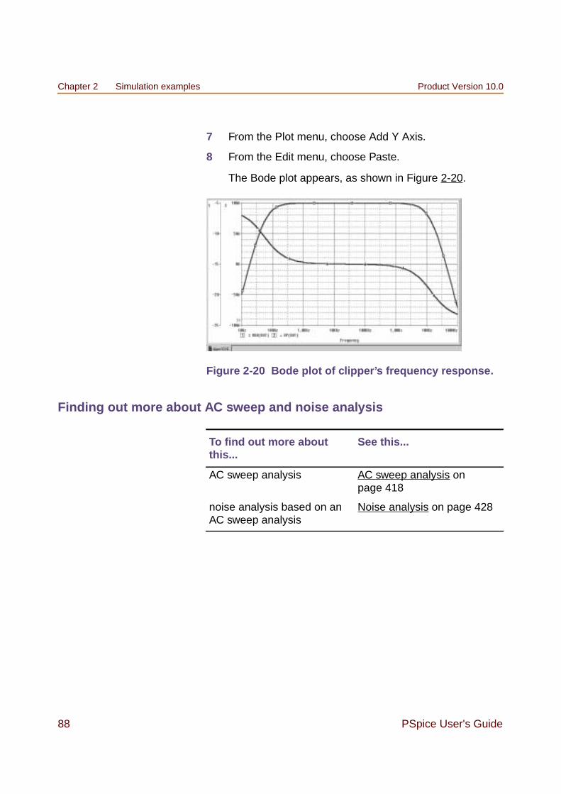
The Bode plot appears, as shown in Figure 2-20.
Figure 2-20 Bode plot of clipper’s frequency response.
Finding out more about AC sweep and noise analysis
To find out more aboutthis...
See this...
AC sweep analysis AC sweep analysis onpage 418
noise analysis based on anAC sweep analysis
Noise analysis on page 428

Product Version 10.0 Transient analysis
PSpice User's Guide 89
Parametric analysis
Note: Parametric analysis is not included in PSpice A/DBasics.
This example shows the effect of varying input resistance onthe bandwidth and gain of the clipper circuit by:
Changing the value of R1 to the expression Rval.
Placing a PARAM part to declare the parameter Rval.
Setting up and running a parametric analysis to step thevalue of R1 using Rval.
Figure 2-21 Clipper circuit with global parameter Rval.
This example produces multiple analysis runs, each with adifferent value of R1. After the analysis is complete, you cananalyze curve families for the analysis runs using PSpice A/D.

Chapter 2 Simulation examples Product Version 10.0
90 PSpice User's Guide
Setting up and running the parametric analysis
To change the value of R1 to the expression Rval
1 In Capture, open CLIPPER.OPJ.
2 Double-click the value (1k) of part R1 to display theDisplay Properties dialog box.
3 In the Value text box, replace 1k with Rval.
PSpice interprets text in curly braces as an expressionthat evaluates to a numerical value. This example usesthe simplest form of an expression—a constant. Thevalue of R1 will take on the value of the Rval parameter,whatever it may be.
4 Click OK.
To add a PARAM part to declare the parameter Rval
1 From Capture’s Place menu, choose Part.
2 In the Part text box, type PARAM (from the PSpice librarySPECIAL.OLB), then click OK.
3 Place one PARAM part in any open area on theschematic page.
4 Double-click the PARAM part to display the Partsspreadsheet, then click New.
For more information about using the Parts spreadsheet,see the OrCAD Capture User’s Guide.
5 In the Property Name text box, enter Rval (no curlybraces), then click OK.
This creates a new property for the PARAM part, asshown by the new column labeled Rval in thespreadsheet.
6 Click in the cell below the Rval column and enter 1k as theinitial value of the parametric sweep.
7 While this cell is still selected, click Display.

Product Version 10.0 Transient analysis
PSpice User's Guide 91
8 In the Display Format frame, select Name and Value, thenclick OK.
9 Click Apply to update all the changes to the PARAM part.
10 Close the Parts spreadsheet.
11 Select the VP marker and press Delete to remove themarker from the schematic page.
Note: This example is only interested in the magnitude ofthe response.
12 From the File menu, choose Save to save the design.
To set up and run a parametric analysis to step the valueof R1 using Rval
1 From Capture’s PSpice menu, chooseNew Simulation Profile.
The New Simulation dialog box appears.
2 In the Name text box, type Parametric.
3 From the Inherit From list, select AC Sweep, then clickCreate.
The Simulation Settings dialog box appears.
The root schematic listed is the schematic pageassociated with the simulation profile you are creating.
4 Click the Analysis tab.

Chapter 2 Simulation examples Product Version 10.0
92 PSpice User's Guide
5 Under Options, select Parametric Sweep and enter thesettings as shown below.
This profile specifies that the parameter Rval is to bestepped from 100 to 10k logarithmically with a resolutionof 10 points per decade.
The analysis is run for each value of Rval. Because thevalue of R1 is defined as Rval, the analysis is run foreach value of R1 as it logarithmically increases from 100Ωto 10 kΩ in 20 steps, resulting in a total of 21 runs.
6 Click OK.
7 From the PSpice menu, choose Run to start the analysis.
Figure 2-22 Parametric simulation settings.
Product Version 10.0 Transient analysis
PSpice User's Guide 93
Analyzing waveform families
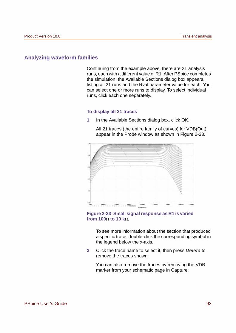
Continuing from the example above, there are 21 analysisruns, each with a different value of R1. After PSpice completesthe simulation, the Available Sections dialog box appears,listing all 21 runs and the Rval parameter value for each. Youcan select one or more runs to display. To select individualruns, click each one separately.
To display all 21 traces
1 In the Available Sections dialog box, click OK.
All 21 traces (the entire family of curves) for VDB(Out)appear in the Probe window as shown in Figure 2-23.
To see more information about the section that produceda specific trace, double-click the corresponding symbol inthe legend below the x-axis.
2 Click the trace name to select it, then press Delete toremove the traces shown.
You can also remove the traces by removing the VDBmarker from your schematic page in Capture.
Figure 2-23 Small signal response as R1 is variedfrom 100Ω to 10 kΩ.

Chapter 2 Simulation examples Product Version 10.0
94 PSpice User's Guide
To compare the last run to the first run
1 From the Trace menu, choose Add Trace to display theAdd Traces dialog box.
2 In the Trace Expression text box, type the following:
Vdb(Out)@1 Vdb(Out)@21
Tip
You can avoid some of the typing for the TraceExpression text box by selecting V(OUT) twice in thetrace list and inserting text where appropriate in theresulting Trace Expression.
3 Click OK.
Note: The difference in gain is apparent. You can also plot thedifference of the waveforms for runs 21 and 1, then usethe search commands to find certain characteristics ofthe difference.
4 Plot the new trace by specifying a waveform expression:
a. From the Trace menu, choose Add Trace.
b. In the Trace Expression text box, type the followingwaveform expression:
Vdb(Out)@1-Vdb(OUT)@21
c. Click OK.
5 Use the search commands to find the value of thedifference trace at its maximum and at a specificfrequency:
a. From the Trace menu, point to Cursor and chooseDisplay.
b. Right-click then left-click the trace part (triangle) forVdb(Out)@1 - Vdb(Out)@21. Make sure that youleft-click last to make cursor 1 the active cursor.
c. From the Trace menu, point to Cursor and chooseMax.

Product Version 10.0 Transient analysis
PSpice User's Guide 95
d. From the Trace menu, point to Cursor and chooseSearch Commands.
e. In the Search Command text box, type the following:
search forward x value (100)
The search command tells PSpice to search for thepoint on the trace where the x-axis value is 100.
f. Select 2 as the Cursor to Move option.
g. Click OK.
Figure 2-24 shows the Probe window with cursors placed.
Note that the Y value for cursor 2 in the cursor box isabout 17.87. This indicates that when R1 is set to 10 kΩ,the small signal attenuation of the circuit at 100Hz is17.87dB greater than when R1 is 100Ω.
6 From the Trace menu, point to Cursor and choose Displayto turn off the display of the cursors.
7 Delete the trace.
Figure 2-24 Small signal frequency responseat 100 and 10 kΩ input resistance.

Chapter 2 Simulation examples Product Version 10.0
96 PSpice User's Guide
Finding out more about parametric analysis
To find out more aboutthis...
See this...
parametric analysis Parametric analysis onpage 438
using global parameters Using global parameters andexpressions for values onpage 117

Product Version 10.0 Transient analysis
PSpice User's Guide 97
Performance analysis
Note: Performance analysis is not available inPSpice A/D Basics.
Performance analysis is an advanced feature in PSpice thatyou can use to compare the characteristics of a family ofwaveforms. Performance analysis uses the principle of searchcommands introduced earlier in this chapter to definefunctions that detect points on each curve in the family.
After you define these functions, you can apply them to afamily of waveforms and produce traces that are a function ofthe variable that changed within the family.
This example shows how to use performance analysis to viewthe dependence of circuit characteristics on a sweptparameter. In this case, the small signal bandwidth and gainof the clipper circuit are plotted against the swept inputresistance value.
To plot bandwidth vs. Rval using the performanceanalysis wizard
1 In Capture, open CLIPPER.OPJ.
2 From PSpice’s Trace menu, choose PerformanceAnalysis.
The Performance Analysis dialog box appears withinformation about the currently loaded data andperformance analysis in general.
Note: The Performance Analysis menu item is onlyavailable if an analysis data file is available. In this case,the data from theparametric analysis of the previousexample should still be open.
3 Click the Wizard button.
At each step, the wizard provides information andguidelines.
4 Click the Next> button.
Chapter 2 Simulation examples Product Version 10.0
98 PSpice User's Guide
5 In the Choose a Goal Function list, click Bandwidth, thenclick the Next> button.
6 Click in the Name of Trace to search text box and typeV(Out).
7 Click in the db level down for bandwidth calc text box andtype 3.
8 Click the Next> button.
The wizard displays the gain trace for the first run(R=100) and shows how the bandwidth is measured. Thisis done to test the goal function.
9 Click the Next> button or the Finish button.
A plot of the 3dB bandwidth vs. Rval appears.
10 Change the x-axis to log scale:
a. From the Plot menu, choose Axis Settings.
b. Click the X Axis tab.
c. Under Scale, choose Log.
d. Click OK.
To plot gain vs. Rval manually
1 From the Plot menu, choose Add Y Axis.
2 From the Trace menu, choose Add to display the AddTraces dialog box.
3 In the Functions or Macros frame, select theMeasurements list, and then click the Max(1) goalfunction.
The Trace list includes measurements expressions onlyin performance analysis mode when the x-axis variable isthe swept parameter.
4 In the Simulation Output Variables list, click V(out).
5 In the Trace Expression text box, edit the text to beMax(Vdb(out)), then click OK.

Product Version 10.0 Transient analysis
PSpice User's Guide 99
PSpice displays gain on the second y-axis vs. Rval.
Figure 2-25 shows the final performance analysis plot of 3dBbandwidth and gain in dB vs. the swept input resistance value.
Figure 2-25 Performance analysis plots of bandwidth andgain vs. Rval.
Finding out more about performance analysis
To find out more aboutthis...
See this...
how to use performanceanalysis
RLC filter example onpage 439
Example: Monte Carloanalysis of a pressure sensoron page 486
how to use searchcommands and createmeasurement expressions
Chapter 18, “Measurementexpressions”