simulation of a magnetron using discrete modulated current
TRANSCRIPT

SIMULATION OF A MAGNETRON USING DISCRETE MODULATED
CURRENT SOURCES
by
Sulmer A. Fernández Gutierrez
A dissertation
submitted in partial fulfillment
of the requirements for the degree of
Doctor of Philosophy in Electrical and Computer Engineering
Boise State University
May 2014

© 2014
Sulmer A. Fernández Gutierrez
ALL RIGHTS RESERVED

BOISE STATE UNIVERSITY GRADUATE COLLEGE
DEFENSE COMMITTEE AND FINAL READING APPROVALS
of the dissertation submitted by
Sulmer A. Fernández Gutierrez
Dissertation Title: Simulation of a Magnetron Using Discrete Modulated Current
Sources Date of Final Oral Examination: 12 March 2014
The following individuals read and discussed the dissertation submitted by student Sulmer A. Fernández Gutierrez, and they evaluated her presentation and response to questions during the final oral examination. They found that the student passed the final oral examination.
Jim Browning, Ph.D. Chair, Supervisory Committee Kris Campbell, Ph.D. Member, Supervisory Committee Wan Kuang, Ph.D. Member, Supervisory Committee Mark Gilmore, Ph.D. External Examiner The final reading approval of the dissertation was granted by Jim Browning, Ph.D., Chair of the Supervisory Committee. The dissertation was approved for the Graduate College by John R. Pelton, Ph.D., Dean of the Graduate College.

iv
DEDICATION
I dedicate this dissertation to my parents, Sulmer and Juan, for their unconditional
love, endless support, and encouragement throughout my studies and life. They taught me
that even the largest task can be accomplished if it is done one step at a time. I also
dedicate this dissertation to my little sister, Cindy, for her love and friendship during my
studies and throughout the years.

v
ACKNOWLEDGEMENTS
I would like to thank Dr. Jim Browning for serving as my major professor and
guide through my Ph.D. program. It was a pleasure to be his first Ph.D. student; I truly
appreciate all the time and advice he gave me throughout my time at Boise State
University. The enthusiasm he has for his research was motivational and encouraging for
me, even during tough times in the Ph.D. pursuit. Thanks for all the valuable insights and
support, which were a major contribution to complete this dissertation. I would also like
to thank Dr. Kris Campbell, Dr. Wan Kuang, and Dr. Mark Gilmore for being willing to
serve as members of my committee. I would also like to acknowledge all the faculty and
staff that I worked with at Boise State University, took classes from, and met throughout
my graduate studies. They were wonderful people and a real pleasure to know. I also
acknowledge the funding sources that made my Ph.D. work possible. The first year this
research was funded by the Air Force Office of Scientific Research (ASFOR) under
Contract No. FA9550-09-C-0141. The remaining time to completion was funded by the
Electrical and Computer Engineering (ECE) Department at Boise State University.
I would like to thank Dr. Jack Watrous for his help, expertise, advice, and useful
discussions about magnetrons. I would also like to acknowledge Tech-X Corporation,
especially Dr. David Smithe, Dr. Ming-Chieh Lin, and Dr. Peter Stoltz for their support
and advice and for setting up the original magnetron model in VORPAL; their help was

vi
instrumental in this dissertation. Dr. David Smithe, thank you for the professional advice,
time you took speaking with me, and overall friendliness.
Thank you to my MVEDs research group: Peter, Marcus, and Tyler, you were
always open for discussion, helping me find errors, and checking my work. I appreciate
your assistance and friendship. Although, we worked in different projects, we were
always able to collaborate with each other.
Finally, I would like to thank my family and friends (too many to list here but you
know who you are!) for providing support and friendship that I needed during my studies,
and also during my study breaks. For anyone else, whom I forgot to mention here, many
thanks.

vii
ABSTRACT
Magnetrons are microwave oscillators and are extensively used for commercial
and military applications requiring power levels from the kilowatt to the megawatt range.
It has been proposed that the use of gated field emitters with a faceted cathode in place of
the conventional thermionic cathode could be used to control the current injection in a
magnetron, both temporally and spatially. In this research, this concept is studied using
the 2-D particle trajectory simulation Lorentz2E and the 3-D particle-in-cell (PIC) code
VORPAL. The magnetron studied is a ten cavity, rising sun magnetron, which can be
modeled easily using a 2-D simulation. The 2-D particle trajectory code is used to model
the electron injection from gated field emitters in a slit type structure, which is used to
protect the gated field emitters. VORPAL is used to study the magnetron performance for
a cylindrical, a five-sided, and a ten-sided cathode. Finally, VORPAL is used to simulate
a modulated, addressable, ten-sided cathode. The aspects of magnetron performance for
which improvements are desired include mode control, efficiency, start oscillation time,
and phase control. The simulation results show that the modulated, addressable cathode
reduces startup time from 100 ns to 35 ns, increases the power density, controls the RF
phase, and allows active phase control during oscillation.

viii
TABLE OF CONTENTS
DEDICATION .................................................................................................................... iv
ACKNOWLEDGEMENTS .................................................................................................. v
ABSTRACT ....................................................................................................................... vii
LIST OF TABLES .............................................................................................................. xi
LIST OF FIGURES ............................................................................................................ xii
CHAPTER ONE: INTRODUCTION ................................................................................... 1
1.1 Overview and Introduction ............................................................................ 1
1.2 Motivation and Contributions ........................................................................ 5
1.3 Dissertation Organization .............................................................................. 6
CHAPTER TWO: BACKGROUND..................................................................................... 8
2.1 Magnetron Operating Characteristics ............................................................. 8
2.2 Cylindrical Magnetron ................................................................................. 12
2.3 Magnetron Resonant Circuit and Modes of Operation .................................. 14
2.4 The Hartree and Hull Cutoff Condition ........................................................ 17
2.5 The Diocotron Instability ............................................................................. 19
2.6 Stability and Mode Separation ..................................................................... 22
CHAPTER THREE: LORENTZ2E SIMULATION ........................................................... 30
3.1 Overview ..................................................................................................... 30
3.2 Software ...................................................................................................... 30

ix
3.3 Simulation Setup and Procedures ................................................................. 31
3.4 Electron Trajectory Analysis ....................................................................... 34
3.5 Sensitivity Simulations ................................................................................ 35
CHAPTER FOUR: LORENTZ2E SIMULATION RESULTS ............................................ 37
4.1 Overview ..................................................................................................... 37
4.2 Energy Distribution Analysis ....................................................................... 37
4.3 Electron Velocity ......................................................................................... 39
4.4 Sensitivity Simulations ................................................................................ 41
4.5 Summary of Results .................................................................................... 54
CHAPTER FIVE: VORPAL SIMULATION SETUP ......................................................... 56
5.1 Overview ..................................................................................................... 56
5.2 Software ...................................................................................................... 56
5.3 Finite Difference Time Domain (FDTD) Technique .................................... 57
5.4 Numerical Stability ...................................................................................... 60
5.5 Boundary Conditions ................................................................................... 61
5.6 Dey-Mittra Cut Cell Algorithm .................................................................... 62
5.7 Integration of the Equations of Motion ........................................................ 64
5.8 Modeling of a 2-D Ten Cavity Rising Sun Magnetron ................................. 64
5.9 Simulation Setup and Procedures ................................................................. 67
5.10 Rising Sun Magnetron Model with a Continuous Current Source ................ 73
5.11 Rising Sun Magnetron Model with Modulated, Addressable, Current
Sources ................................................................................................................... 81
CHAPTER SIX: VORPAL SIMULATION RESULTS FOR THE CONTINUOUS
CURRENT SOURCE CATHODE MODEL ....................................................................... 88

x
6.1 Overview ..................................................................................................... 88
6.2 Continuous Current Source Model: Cylindrical Cathode .............................. 88
6.3 Continuous Current Source Model: Five-Sided Faceted Cathode ................. 92
6.4 Continuous Current Source Model: Ten-Sided Faceted Cathode .................. 99
6.5 Summary of Results .................................................................................. 102
CHAPTER SEVEN: VORPAL SIMULATION RESULTS FOR THE MODULATED,
ADDRESSABLE CATHODE .......................................................................................... 103
7.1 Overview ................................................................................................... 103
7.2 Modulated Five-Sided Faceted Cathode ..................................................... 103
7.3 Modulated Five-Sided Faceted Cathode with Time Overlap ...................... 106
7.4 Modulated Five-Sided Cathode with Time Overlap and DC Hub ............... 110
7.5 Modulated Ten-Sided Faceted Cathode...................................................... 114
7.6 Modulated Ten-Sided Faceted Cathode with DC Hub ................................ 118
7.7 Modulated Ten-Sided Faceted Cathode with Active Phase Control ............ 124
7.8 Summary of Results .................................................................................. 130
7.9 Discussion of Application of Modulated Addressable Cathode .................. 131
CHAPTER EIGHT: SUMMARY AND CONCLUSIONS ................................................ 134
REFERENCES ................................................................................................................. 138
APPENDIX A .................................................................................................................. 152
Lorentz2E Simulations .......................................................................................... 152
APPENDIX B .................................................................................................................. 173
VORPAL Simulation Input Decks......................................................................... 173

xi
LIST OF TABLES
Table 3.1: Lorentz2E Magnetron Model Sensitivity Simulations. ............................ 36
Table 4.1: Voltage sensitivity analysis results for variations in the pusher electrode
voltage.................................................................................................... 43
Table 4.2: Voltage sensitivity analysis results for variations in the emitter voltage. . 45
Table 4.3: Voltage sensitivity analysis results for variations in the pusher electrode
voltage with a pusher electrode thickness of 1.70 µm.............................. 48
Table 4.4: Voltage sensitivity analysis results for variations in the emitter voltage
with a pusher electrode thickness of 1.7 µm. .......................................... 50
Table 4.5: Voltage sensitivity analysis results for variations in the pusher electrode
voltage with a pusher electrode thickness of 0.4475 µm. ......................... 52
Table 4.6: Voltage sensitivity analysis results for variations in the emitter voltage
with a pusher electrode thickness of 0.4475 µm. ..................................... 54
Table 5.1: Rising sun magnetron dimensions for cylindrical, five and ten-sided
faceted cathodes. .................................................................................... 67
Table 5.2: Rising sun magnetron: cylindrical cathode VORPAL simulations. .......... 80
Table 5.3: Rising sun magnetron: faceted cathode VORPAL simulations. ............... 80
Table 5.4: Five-Sided Faceted Cathode Additional Simulation Tests with
Modulated, Addressable Current Sources. .............................................. 87
Table 7.1: Current densities, power densities, and efficiencies for various cathode
geometries: cylindrical, five-sided and ten-sided cathode for the reference
parameters Vca = -22.2 kV, B = 0.09 T, and J’e = 326 A/m. ................... 122

xii
LIST OF FIGURES
Figure 1: Power versus frequency performance of various microwave oscillator
tubes, including backward wave oscillators (BWO) and voltage tunable
magnetrons (VTM). ..................................................................................2
Figure 2: Microwave oven. ......................................................................................3
Figure 3: Microwave radar transmission. .................................................................4
Figure 4: Early type of magnetron: Hull original diode. ...........................................8
Figure 5: Electron motion in a crossed electric and magnetic field diode
configuration showing a cycloidal orbit. ...................................................9
Figure 6: First 10-cm cavity magnetron. The slow wave circuit consists of 6
cavities. .................................................................................................. 11
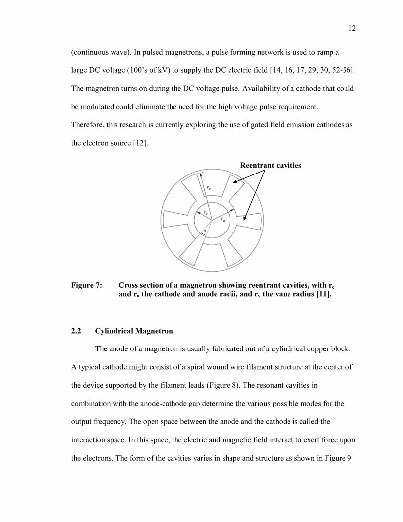
Figure 7: Cross section of a magnetron showing reentrant cavities, with rc and ra the
cathode and anode radii, and rv the vane radius. ...................................... 12
Figure 8: Schematic diagram of a cylindrical magnetron. ....................................... 13
Figure 9: Various forms of the anode block in a magnetron: (a) Slot type, (b) Vane
type, (c) Rising sun, and (d) Hole-and-Slot type...................................... 14
Figure 10: Equivalent circuit of an eight-cavity magnetron. ..................................... 15
Figure 11: Lines of Force in π-mode of Eight-Cavity Magnetron. ............................ 17
Figure 12: Hartree threshold voltage diagram for an eight-cavity ............................. 19
Figure 13: Formation of the spoke-like electron cloud in a ten-cavity rising sun
magnetron from VORPAL simulation. ................................................... 20
Figure 14: Physical mechanism of the diocotron instability...................................... 21
Figure 15: Strapping technique. Alternate anode segments at same potential. .......... 23
Figure 16: Wire strapping system of an S band cavity magnetron. ........................... 23

xiii
Figure 17: Techniques for achieving mode separation.............................................. 24
Figure 18: Sixteen-cavity rising sun magnetron from Ostron Technologies [64]. ..... 25
Figure 19: Proposed ten-cavity rising sun magnetron with a five-sided faceted
cathode. Each plate would have hundreds of slits with gated emitters
beneath. .................................................................................................. 29
Figure 20: (a) Shielded cathode slit. Showing the stacked lateral field emission tips
on each side of the slit, a pusher electrode, the sole electrode (cathode
plate), and the electron trajectories. (b) Faceted cathode showing slits. ... 32
Figure 21: Lorentz2E model of the shielded cathode slit structure. (a) The emitters on
each side, a field emission gate transparent to electrons, a pusher
electrode, the sole electrode, the electrode voltages, and the dimensions;
and, (b) the electron ray trajectories ........................................................ 32
Figure 22: Magnetron model used in Lorentz2E. Five-sided cathode with a smooth
dummy anode showing electron ray traces from a single shielded slit
structure on the left hand side of the top facet. ........................................ 34
Figure 23: Transverse energy distribution from Lorentz2E for 200 electron rays. .... 38
Figure 25: Velocity in the x-direction versus position for 200 electron rays. ............ 40
Figure 26: Velocity in the y-direction versus position for 200 electron rays. ............ 40
Figure 27: Pusher Electrode Voltage at -22.20 kV. Emitter Voltage at (a) -22.20kV,
(b) -22.26 kV, (c) -22.34 kV, and (d) -22.5 kV........................................ 42
Figure 28: Emitter voltage versus current ratio. ....................................................... 43
Figure 29: Emitter Voltage at -22.20 kV. Pusher Electrode Voltage at (a) -22.20 kV,
(b) -22.26 kV, (c) -22.34 kV, and (d) -22.5 kV........................................ 44
Figure 30: Pusher electrode voltage vs. current ratio. ............................................... 45
Figure 31: Pusher Electrode Voltage at -22.20 kV. Emitter Voltage at (a) -22.20 kV,
(b) -22.26 kV, (c) -22.34 kV, and (d) -22.5 kV. Pusher Electrode
Thickness of 1.70 µm. ............................................................................ 47
Figure 32: Emitter voltage vs. current ratio at different pusher electrode voltages. ... 48
Figure 33: Emitter Voltage at -22.20 kV. Pusher Electrode Voltage at (a) -22.20 kV,
(b) -22.26 kV, (c) -22.34 kV, and (d) -22.5 kV. Pusher Electrode
Thickness of 1.70 µm. ............................................................................ 49
xiv
Figure 34: Pusher electrode voltage vs. current ratio at different emitter voltages. ... 50
Figure 35: Pusher Electrode Voltage at -22.20 kV. Emitter Voltage at (a) -22.20 kV,
(b) -22.26 kV, (c) -22.34 kV, and (d) -22.5 kV........................................ 51
Figure 36: Emitter voltage vs. current ratio at different pusher electrode voltages. ... 52
Figure 37: Emitter Voltage at -22.20 kV. Pusher Electrode Voltage at (a) -22.20 kV,
(b) -22.26 kV, (c) -22.34 kV, and (d) -22.5 kV........................................ 53
Figure 38: Pusher electrode voltage vs. current ratio at different emitter voltages. ... 54
Figure 39: Yee model for placing fields on the grid. ................................................ 59
Figure 40: Basic flow for implementation of Yee FDTD scheme without including
particle injection. .................................................................................... 60
Figure 41: Area fractions borrowed by cut cells in the Zagorodnov boundary
algorithm. ............................................................................................... 63
Figure 42: Cylindrical cathode used in VORPAL simulations. ................................. 66
Figure 43: Five-sided faceted cathode used in VORPAL simulations. ...................... 66
Figure 44: Ten-sided faceted cathode used in VORPAL simulations........................ 67
Figure 45: Startup time of a typical magnetron simulation in VORPAL for the
cylindrical cathode ( caV = -26.0 kV, B = 0.12 T, and aJ = 500 A/m).
Stable oscillation is observed around 300 ns. .......................................... 68
Figure 46: Linear current density vs. time for the cylindrical cathode, typical
VORPAL simulation with B field = 0. .................................................... 69
Figure 47: Anode linear current density vs. time during device operation for the
cylindrical cathode, typical VORPAL simulation. ................................... 70
Figure 48: Rising sun magnetron cavity power diagnostic location. ......................... 71
Figure 49: Rising sun magnetron spoke formation. .................................................. 72
Figure 50: Fast Fourier Transform (FFT) of the cavity voltage versus frequency. .... 74
Figure 51: Fast Fourier Transform (FFT) of the cavity voltage versus frequency. .... 74

xv
Figure 52: Example showing calculation of the quality factor Q. (a) Cavity voltage
versus time, (b) Cavity voltage amplitude versus time from VORPAL, for
the cylindrical cathode caV = -26.0 kV, B = 0.12 T, and 'eJ = 500 A/m.76
Figure 53: Cathode-anode voltage versus time for the cylindrical cathode model
from VORPAL. ...................................................................................... 77
Figure 54: Rising sun magnetron simulation with particles after oscillations start and
spokes form. ........................................................................................... 78
Figure 55: (a) Temporal and spatial modulation concept of the current injection,
showing electrons being injected in phase with spokes. (b) Detailed view
of one of the facets showing the ON and OFF emitters. .......................... 83
Figure 56: Modulated current overlap time diagram for the five-sided faceted
cathode. This diagram shows an example with 5 emitters in 1 facet (1
RF period). ............................................................................................. 86
Figure 57: Cylindrical cathode model from VORPAL simulation showing the RF B-
field and π-mode. This result corresponds to Vca = -26.0 kV, B = 0.12 T,
and J’e = 500 A/m. .................................................................................. 90
Figure 58: Cylindrical cathode cavity voltage frequency versus time with moving
window, showing the startup time of the device at 300 ns, and the mode
switching from 650 MHz to the Operating Frequency (π-mode) 960 MHz
from VORPAL. ...................................................................................... 90
Figure 59: Cylindrical cathode Fast Fourier Transform (FFT), over entire simulation
time, of the loaded cavity voltage from VORPAL simulation. This plot
clearly indicates that the π-mode is dominant at the frequency of operation
of 960 MHz. ........................................................................................... 90
Figure 60: Cylindrical cathode VORPAL simulation results for Vc = -26.0 kV, B =
0.12 T, and J’e = 500 A/m. The red dots indicate electron macroparticles.
Figure 61(a) is at 0.012 ns, before oscillation, and Figure 61(b) is at 276
ns, after oscillation starts and the model is stable. ................................... 91
Figure 61: Cylindrical cathode continuous total emitted linear current density versus
time with no applied magnetic field (B=0). ............................................. 91
Figure 62: Cylindrical cathode continuous anode linear current density during device
operation versus time. ............................................................................. 91
Figure 63: Cylindrical cathode (Vca = -22.2 kV, B = 0.09 T, '
eJ = 326 A/m)
continuous anode linear current density during device operation versus
time. ....................................................................................................... 92

xvi
Figure 64: Startup time versus continuous total emitted linear current density for
different cathode geometries: cylindrical and faceted. ............................. 92
Figure 65: Five-sided faceted cathode model from VORPAL simulation showing the
RF B-field and π-mode. This result corresponds to Vca = -22.2 kV, B =
0.09 T, and J’e = 326 A/m. ...................................................................... 93
Figure 66: Five-sided faceted cathode cavity voltage frequency versus time with
moving window, showing the startup time of the device at 200 ns, and
the mode switching from 650 MHz to the operating frequency (π-mode)
957 MHz from VORPAL. ...................................................................... 94
Figure 67: Five-sided faceted cathode Fast Fourier Transform (FFT), over entire
simulation time, of the loaded cavity voltage from VORPAL simulation.
This plot indicates that the π-mode is dominant at the frequency of
operation of 957 MHz. ............................................................................ 94
Figure 69: Comparison of ICEPIC model versus VORPAL model. Vca = -22.2 kV, B
= 0.09 T, and J’e = 326 A/m. The top figures show the cylindrical
cathode model, the middle figures show the five-sided faceted cathode,
and the bottom figures show the ten-sided faceted cathode. .................... 96
Figure 70: Five-sided faceted cathode continuous total emitted linear current density
versus time with no applied magnetic field (B=0) . ................................. 98
Figure 71: Five-sided faceted cathode continuous anode linear current density during
device operation versus time. The periodic current spikes are followed by
spoke collapse. ....................................................................................... 98
Figure 72: Five-sided faceted cathode showing the transition of the spokes during the
current instability. Spokes are shown (a) before current spike at 119.8 ns,
(b) at current spike at 121.32 ns, and (c) after spokes collapse at 143.5 ns.
............................................................................................................... 98
Figure 73: Ten-sided faceted cathode model from VORPAL simulation showing the
RF B-field and π-mode. This result corresponds to Vca = -22.2 kV, B =
0.09 T, and J’e = 326 A/m. ...................................................................... 99
Figure 74: Ten-sided faceted cathode cavity voltage frequency versus time with
moving window, showing the startup time of the device at 110 ns,
showing the operating frequency (π-mode) at 957 MHz from VORPAL.
............................................................................................................. 100
Figure 75: Ten-sided faceted cathode Fast Fourier Transform (FFT), over entire
simulation time, of the loaded cavity voltage from VORPAL

xvii
simulation. This plot indicates that the π-mode is dominant at the
frequency of operation of 957 MHz. ..................................................... 100
Figure 76: Ten-sided faceted cathode continuous total emitted linear current density
versus time with no applied magnetic field (B=0). ................................ 101
Figure 77: Ten-Sided faceted cathode continuous anode linear current density during
device operation versus time. ................................................................ 101
Figure 78: Five-sided faceted cathode showing discrete current sources setup for (a)
0.0987 ns and (b) 0.197 ns. There are five emitters per facet. All emitters
are ON at the same time. ....................................................................... 104
Figure 79: Five-sided faceted cathode with modulated, addressable current sources,
with B field turned OFF. This shows the emitters turning ON in sequence.
The diagrams show one RF period, τRF=1.04 ns, Δt = 1/5 τRF. Frequency
of modulation is 957 MHz. ................................................................... 105
Figure 80: Five-sided faceted cathode with modulated, addressable current sources.
The frequency of modulation is 957 MHz, τRF=1.04 ns, Δt = 1/5 τRF. .... 107
Figure 81: Five-sided faceted cathode with modulated, addressable current sources
plus current overlap. This diagram shows the case for current overlap of
25%. The frequency of modulation is 957 MHz, τRF = 1.04 ns, Δt = 1/5
τRF, τov = 0.0520 ns. .............................................................................. 108
Figure 82: Modulated total emitted linear current density versus time with no applied
magnetic field (B=0) for five-sided faceted cathode with 25% overlap. 109
Figure 83: Modulated anode linear current density versus time during device
operation for the five-sided faceted cathode with 25% overlap, showing
current spike at around 102 ns. ............................................................. 109
Figure 84: Transition of the spokes during the current instability for the modulated,
addressable current sources for the five-sided faceted cathode with 25%
overlap. Spokes are shown (a) before current spike at 110.3 ns, (b) at
current spike at 113.1 ns, and (c) after spokes collapse at 116.3 ns. ....... 109
Figure 85: Fast Fourier Transform (FFT) of the loaded cavity voltage from VORPAL
Simulation for the modulated, addressable, current source for the five-
sided faceted cathode with 25% overlap. This plot indicates that the π-
mode is dominant at the frequency of operation of 957 MHz. ............... 110
Figure 86: Five-sided faceted cathode with modulated, addressable current sources
with current overlap and DC Hub. This diagram shows a current overlap
of 25% (red electrons) and a 5% current DC hub (green electrons). The

xviii
frequency of modulation is 957 MHz, τRF = 1.04 ns, Δt = 1/5 τRF, τov =
0.0520 ns. In this figure, green electrons are shown on top of red electrons;
this is in an interchangeable feature in VORPAL. Green electrons were
chosen to be seen on top to demonstrate the filled up gaps presented with
only modulated and overlap technique. ................................................. 112
Figure 87: Five-sided faceted cathode showing: on the left column the modulated
plus current overlap (25% overlap) simulation electrons and on the right
the DC hub (5% J’e) electrons. It shows the comparison between the two,
and it can be seen that the gaps are filled by the green DC hub electrons.
............................................................................................................. 113
Figure 88: Ten-Sided Faceted cathode showing discrete current sources setup for (a)
0.0163 ns and (b) 0.326 ns. There are three emitters per facet. All emitters
are ON at the same time. ....................................................................... 114
Figure 89: Ten-sided faceted cathode with modulated, addressable current sources,
with B field turned OFF. This shows the emitters turning ON in sequence.
The diagrams show one RF period (two facets), τRF=1.04ns, Δt = 1/6 τRF.
Frequency of modulation is 957 MHz. .................................................. 115
Figure 90: Ten-sided faceted cathode with modulated, addressable current sources.
The frequency of modulation is 957 MHz, τRF=1.04 ns, Δt = 1/6 τRF. .... 116
Figure 91: Modulated total emitted linear current density versus time with no applied
magnetic field (B=0) for ten-sided faceted cathode. .............................. 117
Figure 92: Modulated anode linear current density versus time during device
operation for the ten-sided faceted cathode. .......................................... 117
Figure 93: Modulated ten-sided faceted cathode cavity voltage frequency versus
time with moving window, showing the startup time of the device at 50 ns
showing the operating frequency (π-mode) at 957 MHz from VORPAL.
............................................................................................................. 118
Figure 94: Fast Fourier Transform (FFT), over entire simulation time, of the loaded
cavity voltage from VORPAL simulation for the modulated,
addressable, current source, ten-sided faceted cathode. This plot
indicates that the π-mode is dominant at the frequency of operation of
957 MHz. ............................................................................................. 118
Figure 95: Ten-sided faceted cathode with modulated, addressable current sources
with DC Hub. This diagram shows a 5% current DC hub (green electrons).
The frequency of modulation is 957 MHz, τRF = 1.04 ns, Δt = 1/6 τRF.... 119

xix
Figure 96: Comparison of startup time versus total emitted linear current density for
different cathode geometries: cylindrical and faceted, including continuous
current source model and the modulated, addressable current source model
for the ten-sided faceted cathode. .......................................................... 120
Figure 97: Anode current density versus total emitted linear current density for the
ten-sided faceted cathode with continuous current source and modulated
current source. ...................................................................................... 122
Figure 98: Loaded cavity power versus total emitted linear current density for the ten-
sided faceted cathode with continuous current source and modulated
current source. ...................................................................................... 123
Figure 99: Efficiency versus total emitted linear current density for the ten-sided
faceted cathode with continuous current source and modulated current
source. .................................................................................................. 124
Figure 100: Ten-sided faceted cathode with (a) Modulated, addressable current
sources: Spokes are aligned at the same location in time (76.38 ns) for
three different simulation runs, (b) Continuous current source: Spokes are
not aligned at the same location in time (322.12 ns) for three different
simulation runs. .................................................................................... 125
Figure 101: Ten-sided faceted cathode with modulated addressable current sources,
showing transition to a phase shift of 180°. (a) Reference case: Phase = 0°
at 82.0 ns, phase shift initiated at 88.40 ns, (b) after 14.5 RF periods (t =
96.8 ns) from the reference, 8 RF periods from the phase shift, (c) after 17
RF periods (t = 100.0 ns), 11 RF periods from the phase shift, (d) after 35
RF periods (t = 118.4 ns), 29 RF periods from the phase shift. .............. 126
Figure 102: RF Bz field vs. reference time; showing transition to a phase shift of 180°
initiated at 88.40ns. Reference: Phase=0° (a) After 14.5 RF periods
(t=96.8ns) from reference, 8 RF periods from phase shift, (b) after 17 RF
Periods (t=100.0ns) from reference, 11 RF periods from phase shift, (c)
after 35 RF Periods (t=118.4ns) from reference, 29 RF periods from phase
shift. ..................................................................................................... 128
Figure 103: Modulated ten-sided faceted cathode cavity voltage frequency versus
time, showing the startup time of the device with phase shift initiated at
88.40 ns. The operating frequency (π-mode) is at 957 MHz from
VORPAL.............................................................................................. 129
Figure 104: Phase versus RF Periods. Curve for the ten-sided faceted cathode with
modulated, addressable current sources. The phase shift is initiated at
88.40 ns. The RF periods for this plot are counted after the phase shift. 130

1
CHAPTER ONE: INTRODUCTION
1.1 Overview and Introduction
Radio frequency (RF) radiation has improved the way people live in a variety of
ways. Microwave ovens, cell phones, satellite communications, radar, global positioning
systems, and air traffic are among the many applications. RF radiation is generated using
solid-state and vacuum devices. Microwave devices are capable of high output power
(GW-class) with applications over a wide range of frequencies [1-5]. Figure 1 shows a
graph of power versus frequency performance [6] of various Microwave Vacuum
Electron Devices (MVEDs). This graph shows the range of output power that can be
achieved with various devices depending on their frequency of operation. The magnetron
was the first practical microwave device, and it allowed the development of microwave
radar during World War II [1, 7-10]. Since then, many microwave devices have been
developed for the generation and amplification of microwave radiation.
One type of MVED, the crossed-field device, is also called the M-type tube after
the French TPOM (tubes à propagation des ondes à champs magnétique: tubes for
propagation of waves in a magnetic field) [5]; this name derives from the concept that the
DC electric field and the DC magnetic field are perpendicular to each other. This
dissertation is concerned with the magnetron, which is one type of crossed-field device.
Magnetrons are oscillators that can be designed to operate over a wide frequency range,
to have high efficiency, and to operate at high power levels. The magnetrons can be

2
continuous-wave (CW) or pulsed. Pulsed magnetrons can generate very high powers
(MW) [2, 6, 11]
Figure 1: Power versus frequency performance of various microwave
oscillator tubes, including backward wave oscillators (BWO) and
voltage tunable magnetrons (VTM) [6].
Magnetrons have the advantage of being able to generate high power (from
kilowatts to megawatts) at high efficiency (40 to 70%) [5]. Magnetrons are used in
numerous applications such as: communications, radar, warfare, medical X-ray sources,
and microwave ovens. Figure 2 shows the magnetron as used in a microwave oven. As is
shown in the figure, the microwave oven system consists of a microwave source, a
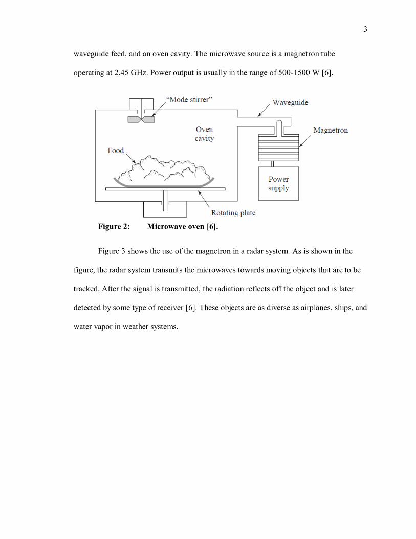
3
waveguide feed, and an oven cavity. The microwave source is a magnetron tube
operating at 2.45 GHz. Power output is usually in the range of 500-1500 W [6].
Figure 2: Microwave oven [6].
Figure 3 shows the use of the magnetron in a radar system. As is shown in the
figure, the radar system transmits the microwaves towards moving objects that are to be
tracked. After the signal is transmitted, the radiation reflects off the object and is later
detected by some type of receiver [6]. These objects are as diverse as airplanes, ships, and
water vapor in weather systems.

4
Figure 3: Microwave radar transmission [6].
Magnetrons have been important in the military, commercial, and the plasma
physics research communities since the 1940s. There has been a continuing interest in
improving performance such as efficiency, power density, start up times, phase locking,
and high frequency operation [12-17]. One technique that can help improve these aspects
is being developed in this dissertation research. This dissertation involves the simulation
of a 2-D model of a ten-cavity rising sun magnetron device using the particle-in-cell
(PIC) code VORPAL [18]. The use of gated vacuum field emitters [19, 20] (referred to as
discrete current sources in this work) was proposed in a prior work [12] to replace
conventional thermionic cathodes used in magnetrons today. This approach would allow
control of the electron current injection. The final goal of this dissertation is to perform a
temporal and spatial modulation study of the discrete electron sources of the faceted
magnetron and to demonstrate phase control of the device.
Radar Transmit/Receive Antenna
Microwave Radiation
Wave Guide
Resonant-Cavity Magnetron
Moving Object

5
1.2 Motivation and Contributions
This dissertation consists only of simulation work. An overview of the
characteristics of magnetron modeling, the problems presented with simulation analysis,
and the contributions of this dissertation to the state of magnetron research are discussed
in this section.
Magnetrons are difficult to model. They usually require 3-D rather than 2-D
modeling. This dissertation presents a 2-D model of a ten-cavity rising sun magnetron
using the electron trajectory code Lorentz2E [21] and the particle-in-cell code (PIC)
VORPAL [22]. The rising sun geometry can be easily modeled in 2D, which greatly
reduces computation time, and it does not require a complex magnetron model such as
the strapped magnetron (see Chapter 2), which can only be modeled in 3-D simulations.
Although a 2-D simulation is not the most accurate representation of the device, it is
accurate enough [23, 24] to study the device operation, mode separation, and other
variables of magnetron performance. There are several different particle-in-cell (PIC)
codes available for this type of study; these simulations will be covered in more detail in
Chapter 5.
The objective of this research is to demonstrate, via simulation, phase control of
the magnetron by implementing a modulated, addressable current source to control the
current injection of the device, in place of the traditional thermionic cathodes. This
design offers a number of possible advantages: (1) the discrete current sources (emitters)
provide a distributed cathode, (2) the electron source can be turned ON and OFF rapidly
(<1 ns), and (3) the sources provide the means to spatially and temporally control the
current injection. The use of gated field emitters [12] allows temporal modulation of the
6
electrons, which can be used to control the startup time of the device and to phase control
the magnetron. The work presented in this dissertation does not cover phase control of
multiple, coupled magnetrons [25-28]; it is focused on the phase control of one
magnetron device.
The following contributions were achieved as part of this research:
1) Lorentz2E [21] analysis of electron injection and sensitivity of the injection to
operating voltage and electrode location.
2) Development of a faceted cathode model with discrete current sources. This
model includes the development of a stable simulation using the particle-in-cell (PIC)
code VORPAL [22].
3) Development of a model that controls the device oscillations: temporal and
spatial modulation with phase control. This is the major contribution to magnetron
research. This model demonstrates phase control of the magnetron oscillations and,
moreover, the control of performance of the device. It includes a detailed analysis of
magnetron performance under these conditions and analysis of the model stability and
possible causes of erratic behavior.
1.3 Dissertation Organization
The remainder of this dissertation is organized into seven additional chapters:
Chapter 2 gives an introduction to the operating principles of magnetron devices.
It provides a background and history of the device and describes the circuit model and
basics of magnetron operation.
Chapter 3 describes in detail the Lorentz2E software and the simulation setup.
7
Chapter 4 presents the simulation results obtained with Lorentz2E. It describes the
electron trajectory analysis and the sensitivity analysis.
Chapter 5 gives an introduction to PIC codes. It describes the Finite-Difference
Time-Domain (FDTD) method, numerical stability, boundary conditions, and techniques
implemented in VORPAL. This chapter introduces the 2-D model of the rising sun
magnetron and the simulation setup.
Chapter 6 and Chapter 7 present extensive simulation work, analysis, and results
obtained with VORPAL. The results are divided in two models: the continuous current
source, or reference model, and the modulated, addressable, current source model. The
continuous current source model is presented in Chapter 6. The temporal modulation and
phase control are presented in Chapter 7.
Chapter 8 includes the summary, conclusions, and proposed future work.

8
CHAPTER TWO: BACKGROUND
2.1 Magnetron Operating Characteristics
Magnetrons are crossed-field microwave sources that are capable of achieving an
output of hundreds of megawatts [29, 30]. They have a rich history beginning in the
1920s with the work by Hull, who investigated the behavior of electrons in a cylindrical
diode in the presence of a magnetic field parallel to its axis [1, 8, 10, 13, 30-37]. Figure 4
shows Hull‟s original diode.
Figure 4: Early type of magnetron: Hull original diode [1].
A cylindrical anode surrounds the cathode (thermionic), which is heated to
provide a source of electrons. A uniform magnetic field parallel to the axis of the tube is
produced by a solenoid or external magnet not shown in the diagram. In the crossed
electric and magnetic field, which exists between the cathode and anode, an electron that
is emitted by the cathode moves under the influence of the Lorentz force:

9
( )q q F E v B (2.1)
where E is the electric field, B the magnetic field, v the velocity of the electron, and q
is its charge [1, 5]. Figure 5 shows the electron motion in a crossed electric and magnetic
field. The circular orbit, which turns around at the cathode, is referred to as a “cycloidal
orbit.”
Figure 5: Electron motion in a crossed electric and magnetic field diode
configuration [5] showing a cycloidal orbit.
The solution of the resulting equations of motion, which neglect space-charge
effects, shows that the path of the electron is a quasi-cycloidal orbit with a frequency
given approximately by
t
ef B
m (2.2)
where m is the particle mass and e is the electron charge.
A condition of “cutoff” is said to be present when the trajectory of this orbit
touches the anode; therefore, the following equation can be written as:

10
22
2
21
8
o ca
a
V rer
B m r
(2.3)
where oV is cathode-anode voltage, and ar and
cr are the anode and cathode radii [1, 5],
respectively (See Figure 5). This equation implies that for Vo/B2 less than the right hand
side of the equation there is no current flowing, and therefore, the electrons will not reach
the anode. On the other hand, if Vo/B2 increases to the condition of cutoff, an increase in
the current is observed. Equation 2.3 is also called the Hull cutoff voltage equation [5].
The Hull magnetron was not a very successful device. The device had low efficiency, low
power, and erratic behavior. The Hull magnetrons were not fabricated in great quantities,
although they were used for research purposes by Zarek, Yagi, and Cleeton [1].
After the Hull magnetron, in 1935, K. Posthumous [38] studied a different anode
structure for the magnetron with the idea of improving the device efficiency. He
discovered that by using high magnetic fields, the RF power was generated with
relatively high efficiency. After various experiments, an efficiency of 50% was found in a
magnetron operating at a wavelength of 50 cm (600 MHz) [30, 33, 34]. These types of
magnetrons were called traveling-wave oscillators. Continuing Posthumous work, A. L.
Samuel [39] performed experiments with a magnetron using an anode structure called
the hole-and-slot resonator, which provided high frequencies. In 1938, the structure was
again modified by scientists Aleksereff and Malearoff [40]. The magnetron was built
with a copper anode and hole-slot resonators. This device generated a power of about 100
W at a wavelength of 100 cm [30, 33, 34]. Following this, the magnetron became very
important world-wide with the work by Randall and Boot at the University of
Birmingham (UK) [7-9, 41-47] in 1939; their work with the magnetron device became

11
useful in radar applications during World War II. Randall and Boot built a magnetron
with an anode containing six resonant cavities, and they called this device the cavity
magnetron (see Figure 6) [7, 46, 48]. These cavities generate an RF wave that travels at a
phase velocity much less than the speed of light in order to allow for good
synchronization with the electrons. This type of anode structure is called a slow wave
circuit. In early 1940, an experimental radar system containing a cavity magnetron was in
operation. Since then, many microwave devices have been developed for the generation
and amplification of microwave radiation [34].
Figure 6: First 10-cm cavity magnetron [1]. The slow wave circuit
consists of 6 cavities.
Currently, a typical magnetron is comprised of a coaxial structure with an
electron-supplying cathode at the center and a slow-wave structure on the outside [12,
49]. The slow-wave structure in a magnetron usually consists of N resonators spaced
around a cylindrical cavity, or as it is also known, a reentrant cavity. A simple example of
such a six-cavity magnetron is shown in Figure 7.
Conventional magnetrons typically use thermionic cathodes [50] in which
electrons are emitted from a high temperature cathode material in either a space charge or
temperature limited regime. Field emission cathodes [51] are also used in high power
magnetrons, but these emitters are un-gated. Magnetrons can be either pulsed or CW
12
(continuous wave). In pulsed magnetrons, a pulse forming network is used to ramp a
large DC voltage (100‟s of kV) to supply the DC electric field [14, 16, 17, 29, 30, 52-56].
The magnetron turns on during the DC voltage pulse. Availability of a cathode that could
be modulated could eliminate the need for the high voltage pulse requirement.
Therefore, this research is currently exploring the use of gated field emission cathodes as
the electron source [12].
Figure 7: Cross section of a magnetron showing reentrant cavities, with rc
and ra the cathode and anode radii, and rv the vane radius [11].
2.2 Cylindrical Magnetron
The anode of a magnetron is usually fabricated out of a cylindrical copper block.
A typical cathode might consist of a spiral wound wire filament structure at the center of
the device supported by the filament leads (Figure 8). The resonant cavities in
combination with the anode-cathode gap determine the various possible modes for the
output frequency. The open space between the anode and the cathode is called the
interaction space. In this space, the electric and magnetic field interact to exert force upon
the electrons. The form of the cavities varies in shape and structure as shown in Figure 9
Reentrant cavities

13
[57]. In Figure 9, four different cavity types are shown ranging from simple slots to the
hole and slot type. The output port is usually a probe or loop extending into one of the
cavities and coupled into a waveguide or coaxial line (see output from Figure 8) [57].
The cylindrical magnetron is also known as the conventional magnetron. Figure 8
shows a schematic diagram of a cylindrical magnetron oscillator. In this device, several
reentrant cavities (see Figure 7) are connected to the gaps. The DC voltage, Vo, is applied
between the cathode and the anode. For most magnetrons, the cathode is actually biased
at a negative voltage while the anode (slow wave circuit) is held at ground potential. The
magnetic flux density, B, is in the positive z direction as shown in Figure 5. When the DC
voltage and the magnetic flux are adjusted properly, the electrons will follow cycloidal
paths (see Figure 5) in the cathode-anode space under the combined force of both the
electric and magnetic fields [5].
Figure 8: Schematic diagram of a cylindrical magnetron [5].
The magnetron is comprised of a resonant system; therefore the magnetron can
operate at a different number of resonant frequencies. In order to guarantee the stable
operation of the magnetron, it is important to find the right frequency of operation. In the

14
process of finding this frequency, changes in the operation modes will be observed [58].
These aspects will be discussed in Section 2.3.
Figure 9: Various forms of the anode block in a magnetron: (a) Slot type, (b)
Vane type, (c) Rising sun, and (d) Hole-and-Slot type [57].
2.3 Magnetron Resonant Circuit and Modes of Operation
The magnetron is comprised of resonant cavities, and these cavities can be
modeled as resonant circuits. An equivalent circuit for one of the cavity resonators could
be designed as a simple parallel circuit. Figure 10 shows an example of an eight-cavity
magnetron with the oscillating circuit. L and C are inductance and capacitance,
respectively, representing a single cavity. C is the capacitance between the individual
anode segment and the cathode. The coupling from one cavity to another in the end
spaces is represented by M in the circuit [1, 58].

15
Figure 10: Equivalent circuit of an eight-cavity magnetron [1].
The oscillation frequency corresponding to one individual resonator is:
1
oLC
(2.4)
where o is the oscillation frequency, and L and C are the inductance and capacitance
of the individual resonator.
Since the eight cavities have a symmetric distribution, the phase differences (labeled
as ) between adjacent cavities are the same. The voltage between the anode vanes in
each cavity can be represented as [1]:
1 sin( )m oV V t (2.5)
2 sin( )m oV V t (2.6)
3 sin( 2 )m oV V t (2.7)
…
8 sin( 7 )m oV V t (2.8)
9 sin( 8 )m oV V t (2.9)
16
where mV is the amplitude of the RF voltage.
When the system is oscillating, 9V should be equal to
1V . Therefore, 8φ = 2πn (n
= 0,1,2…). The total number of cavities is N, and in order for oscillations to occur the
phase condition is given by
2N n ; (2.10)
therefore, the phase shift between two adjacent cavities can be expressed as:
2
n
n
N
(2.11)
where n is an integer indicating the nth mode of oscillation. In order for oscillations to be
produced in the device, the cathode DC voltage and the applied magnetic field must be
tuned so that the average rotational velocity of the electrons corresponds to the phase
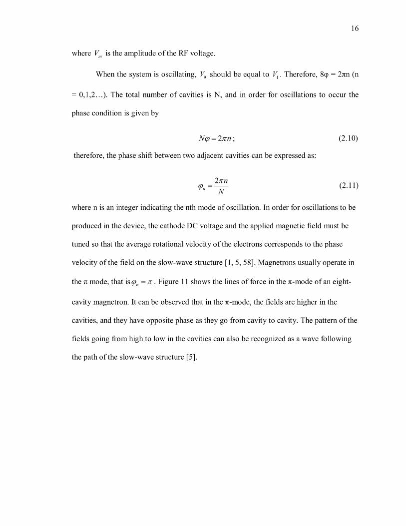
velocity of the field on the slow-wave structure [1, 5, 58]. Magnetrons usually operate in
the π mode, that is n . Figure 11 shows the lines of force in the π-mode of an eight-
cavity magnetron. It can be observed that in the π-mode, the fields are higher in the
cavities, and they have opposite phase as they go from cavity to cavity. The pattern of the
fields going from high to low in the cavities can also be recognized as a wave following
the path of the slow-wave structure [5].

17
Figure 11: Lines of Force in π-mode of Eight-Cavity Magnetron [5].
2.4 The Hartree and Hull Cutoff Condition
There are specific conditions between the applied anode voltage and the static
magnetic field that must be satisfied for a magnetron to operate correctly. In the
cylindrical magnetron, in order for an electron to reach the anode, the condition, known
as “cutoff”, is
22
2 2
21
8
ch a
a
reV B r
m r
(2.12)
where hV is the cutoff cathode-anode voltage, cr is the cathode radius, ar is the anode
radius, and B is the cutoff static magnetic field.
When the RF field is not present and there is a given magnetic field and the
cathode-anode voltage is smaller than hV , the electrons will not touch the anode. This
voltage, hV , is known as the Hull cutoff voltage [5, 58]. If the magnetron operates below
the Hull cutoff voltage, an electron cloud, or hub, will be formed between the cathode

18
and the anode. To start oscillations in the magnetron, it is necessary that the electrons
rotate synchronously with the RF field; thus,
e
n
(2.13)
where e is the angular frequency of electron, is the angular frequency of the RF
field, / n the rotating frequency of the corresponding traveling wave, and n is the mode
number of the traveling wave.
Applying this synchronous condition to the equations of electron motion:
22
2 r z
d r d e e dr E rB
dt dt m m dt
(2.14)
21z
d d e drr B
r dt dt m dt
(2.15)
which govern the electron movement in a cylindrical coordinate system with φ = angle in
cylindrical coordinates; the threshold voltage for oscillation to start in a magnetron can be
obtained [58]:
22 2 2
21
2 2
a c at z
a
r r r mV B
r n e n
(2.16)
The threshold voltage is also known as the Hartree voltage. This voltage is the
condition at which oscillations should start, where B is sufficiently large so that the
undistorted space charge does not extend to the anode. Figure 12 shows the Hartree
Threshold Voltage curve for an eight-cavity magnetron. When the anode voltage is
slightly above the Hartree voltage curve, the magnetron starts to oscillate. In general, the
cathode-anode voltage of a magnetron is always set below the π-1 mode line (n = 3 in
Figure 12) to avoid mode competition.

19
Figure 12: Hartree threshold voltage diagram for an eight-cavity
magnetron © 1976 IEEE [48].
2.5 The Diocotron Instability
The diocotron instability is a perturbation that generally occurs in magnetron
operation. In a magnetron, electrons leave the cathode and are accelerated toward the
anode, due to the DC field established by the voltage source. The magnetic field applied
between the cathode and anode produces a force on each electron that is perpendicular to
the electric field and the electron velocity vectors; this effect causes the electron
trajectories to bend and travel away from the cathode in a cycloidal pattern (see Step 1 in
Figure 13). Following this behavior, the electrons eventually form a rotating cloud around
the cathode, which is also known as the hub (see Step 2 in Figure 13). The hub will

20
continue to rotate around the cathode, and a perturbation, such as the diocotron
instability, will cause the distortion of the electron hub. The rotating perturbation, or
bump, results in a time varying electric and magnetic field from the moving charge. This
field interacts with the slow wave circuit resulting in a circuit field with a rotational phase
velocity that is synchronous with the motion of the electrons. This field causes further
bunching of the electron perturbation or electron bump. In the case of a ten-cavity
magnetron operating in the π-mode, 5 bumps will be formed. As these perturbations
generate time varying electric and magnetic fields, the fields will grow until spokes form
and full oscillation occurs. In Figure 13, this phenomenon can be observed; Step 4 shows
the complete spokes. The formation of these spokes is also an indicator that the device
started oscillating.
Figure 13: Formation of the spoke-like electron cloud in a ten-cavity rising
sun magnetron from VORPAL simulation.
The diocotron instability was one of the first instabilities to be studied since the
beginning of magnetron design [2, 59, 60]. Also, it has been considered the main factor
responsible for noise generation in crossed-field devices. Figure 14 shows a conceptual
example of the diocotron instability [2]. In this example, there are three steps that

21
describe this mechanism. Figure 14a shows the electron sheet; Figure 14b shows the
sinusoidal perturbation applied to the system; and points A and C represent electrons that
are moved upward by the electrostatic force of the adjacent electrons. The electrons
located at points B and D are moved downward. In Figure 14c, it can be observed that
charge bunching is generated by the movement of electrons in A and C to the left and B
and D to the right due to the F B force (Figure 14b). This charge bunching will
increase the growth of the perturbation leading to an E B drift [2].
Figure 14: Physical mechanism of the diocotron instability.
(a) Velocity shear generated by the self-electric field of the electron
sheet, (b) Initial sinusoidal perturbation of the electron sheet, and (c)
growth of the electron-bunching and instability development [2].

22
2.6 Stability and Mode Separation
Magnetrons may have several modes of oscillation. Usually the desired operating
mode in a magnetron is the π mode because it gives better stability and higher output
power. In this section, different techniques for mode separation will be described.
Frequency and Mode Competition
Magnetrons are comprised of many resonators coupled together. For this reason,
mode competition is a common problem in magnetrons [2, 6, 58]. The mode number is
defined as „n‟, and it describes the number of times the RF field pattern is repeated going
around the anode once. N is defined as the number of cavities, where the maximum
number for n is N/2, for π-mode operation. When this occurs, this mode is called the π-
mode [34]. A magnetron operating in the π-mode has greater power output and is the
most commonly used. For this reason, mode separation became very important for
making magnetron oscillators reliable and efficient.
One of the most common problems in the design of magnetrons is to ensure that
the operation remains in only one of the many possible resonant frequencies. It has been
found that this can be achieved if the circuit is designed so that the operating resonant
frequency is well separated from all other resonant frequencies of the structure [61]. Two
techniques, the use of straps and the rising sun structure, are used to achieve mode
separation. These techniques will be described in the following sections.
Strapping
This technique consists of having alternate anode segments connected at the same
RF potential, as shown in Figure 15. These alternate anode segments are connected by a
wire or a strap in which the ends are at the same potential. The use of straps adds extra

23
capacitance to the resonator circuit of each cavity, and therefore it could also add some
undesired modes. However, the strapping technique is designed to separate and isolate
the π-mode frequency; therefore, other frequencies that could be generated are not
significant in comparison to the π-mode. This way the device will not operate in other
modes. Strapping was one of the first techniques used in magnetron design and was first
implemented by Randall and Boot in 1941 in the cavity magnetron [7]. Figure 16 shows a
picture of a strapped magnetron. The wire straps are visible in the image.
Figure 15: Strapping technique. Alternate anode segments at same potential.
Figure 16: Wire strapping system of an S band cavity magnetron [58].
Straps

24
Rising Sun Geometry
The magnetron design for this work is the rising sun magnetron [61-63]. This
design was developed in the search for a stable magnetron operation at wave-lengths
close to 1 cm. This design can also achieve stability and can operate in the π-mode
without strapping [1, 61-63].
The rising sun anode structure was developed by Millman and Nordsieck [61] in
1944. This design utilizes two different resonator sizes arranged symmetrically around
the cathode-anode space, with resonators alternately larger and smaller (See Figure 17).
The rising structure has a design that allows mode separation. By examining the field
patterns that are associated with different modes, it can be observed that modes that range
in the low frequencies are control by the larger cavities. On the other hand, modes
associated with higher frequencies are control by the shorter cavities. Hence, the π-mode
frequency range can be found in between the resonant frequencies of the two cavities [34,
61]. Figure 17 shows a comparison of the strapped structure versus the rising sun
structure.
Figure 17: Techniques for achieving mode separation [61].
Straps Unstrapped Rising Sun

25
The rising sun magnetron is an easier geometry to handle in terms of modeling
and calculations, since the technique of strapping requires a more complex model, and
the calculations that could be done in two-dimension modeling are very limited. The
rising sun geometry allows modeling of the magnetron in two dimensions and, therefore,
greatly reduces computation time. Figure 18 shows a picture of a sixteen-cavity rising sun
magnetron.
Figure 18: Sixteen-cavity rising sun magnetron from Ostron Technologies [64].
2.7 Phase Locking of Magnetrons
Phase locking of magnetrons is a technique used to control the magnetron
oscillation and is also used to take advantage of magnetrons that operate at lower powers.
These magnetrons can be synchronized together and can be „phase locked‟ to a desired
phase with the objective of getting a higher power output. Phase locking is used in many
applications [26-28, 47, 65] ranging from radar systems to materials processing. The idea
is to minimize cost, to take advantage of lower power devices, and to achieve high
efficiency. If a group of 100 kW commercial magnetrons could generate power

26
equivalent to that of a single relativistic magnetron, which is an expensive device, then
phase locking could be used to substitute for this expensive device [25]. Phase locking
has been studied since World War II with the works of Adler [66] and David [67]. They
developed theories applied to phase locking of magnetrons driven by an external source,
which was performed by power injection at levels significantly below the magnetron‟s
output power [25]. The condition for locking is known as Adler‟s condition and is written
as [66]
2 D oD
O o
PQ
P
(2.17)
where DP is the magnitude of injected power, OP is the oscillator‟s output power, D is
the frequency of the injected signal, o is the free running oscillators output frequency,
and Q is the quality factor of the oscillator. The work presented in this dissertation will
not cover phase control of multiple magnetrons, which is a technique broadly covered in
the literature [2, 25-28, 47, 65, 68]; it will focus on the phase control of oscillations of
one magnetron device by using modulated, addressable, controlled electron sources.
2.8 State of the Art and New Magnetron Concept
Ongoing research has been studying different methods to improve magnetron
performance. A group at the University of Michigan has completed extensive research to
improve startup time of oscillations by using two techniques: cathode priming [63] and
magnetic priming [69, 70]. Cathode priming consists of using discrete regions of electron
emission periodically arranged azimuthally along the cathode surface. Emission from
these regions resulted in faster formation of electron bunches. The magnetic priming used

27
an azimuthally modulated magnetic field, which led to modulation of the electrons over
the solid cathode surface. The group is currently studying two new magnetron concepts:
the inverted magnetron and the recirculating planar magnetron [3, 14, 15]. The inverted
magnetron [15], as its name implies, consists of having the cathode on the outside and the
anode on the inside. The main characteristics of this device are its larger cathode area, the
reduction of electron end loss, and a faster startup in comparison with the conventional
magnetron. These characteristics are also incorporated in the recirculating planar
magnetron. The recirculating planar magnetron [14] is considered a new class of crossed-
field device that features both large area cathode and anode, meaning high current and
improved thermal management. This device was designed with 12 cavities, 2 planar
oscillators with 6 cavities each, operating at a frequency of 1 GHz. Mode control is still
under study with this device; using the PIC code MAGIC, they have simulated phase
locking, achieving an increase in mode separation and a reduction in the startup time of
oscillations.
The University of New Mexico developed the transparent cathode technique [16,
17, 71]. This concept also resulted in faster startup times by combining different priming
mechanisms: cathode priming, magnetic priming, and electric priming. The emitters act
as discrete emission centers azimuthally about the cathode. The number and position of
the emitters with respect to the anode cavities may be selected in order to provide the
cathode priming in the desired operating mode [16]. PIC simulations with the transparent
cathode have shown improvements in the output characteristics such as: higher output
power, higher efficiency, and better stability of oscillations. One of the disadvantages of
this technique is that the electron sources cannot be controlled once the device is in

28
operation, since it does not allow a rapid turn ON/OFF time of the current source.
Therefore, it would not allow the temporal modulation of the current sources.
The Air Force Research Lab (AFRL) developed a method to replace thermionic
cathodes with explosive field-emission cathodes [51, 72]. The explosive field emission
cathodes are lightweight; they deliver high currents and do not require heat for their
operation. Three different types of cathodes were tested, each of them with slightly
different geometries. Although, these cathodes are not as developed as thermionic
cathodes, the results demonstrated that this technique provided a lower turn-on DC
electric field and a uniform emission. Moreover, the use of gated field emitters has also
been implemented to replace the conventional thermionic cathode. One of the few
applications of gated field emitters in MVEDs has been implemented in traveling wave
tubes (TWTs) [73, 74]. This project successfully demonstrated the use of modulated
gated emitters in TWTs. The emitters cathode pulse time was reduced from the scale of
seconds (thermionic cathode) to the scale of nanoseconds (gated emitters). It was
demonstrated that the use of gated emitters has the potential to improve TWTs
performance that is not achievable with conventional thermionic cathodes.
The proposed magnetron concept for this research is based on using gated field
emitters placed in a shielded structure housed within the cathode to prevent ion
bombardment to the emitters and to keep the emitters protected from the high electric
field environment of the magnetron [12]. Because the emitters must be fabricated on flat
surfaces, the cathode is comprised of facet plates with slits [12]. This device concept is
shown in Figure 19. The design here shows a ten-cavity rising sun magnetron with a
pentagon shaped cathode with five facet plates. Each facet has slits for electron injection.

29
The front of each facet is a conductor, which forms the sole electrode. Here, the sole
electrode indicates a non-emitting cathode structure. While this image shows a few large
slits, the actual device concept would have hundreds of slits per facet plate with many
thousands of gated emitters placed below the facet. The idea behind this concept is that
the gated field emitters could be used to control the electron injection into the interaction
space of the magnetron by varying the emission current both spatially and temporally.
Hence, the cathode can be modulated to control the beam wave interaction and the device
phase. This modulated, addressable-cathode based magnetron is actually an amplifier but
is based on the cavity magnetron structure. Such a device can reduce start up times and
allow phase locking with other similar devices for increased power output [26, 28, 47].
Figure 19: Proposed ten-cavity rising sun magnetron with a five-sided
faceted cathode. Each plate would have hundreds of slits with gated
emitters beneath.
Anode Cathode
Slits

30
CHAPTER THREE: LORENTZ2E SIMULATION
3.1 Overview
This chapter describes the simulation setup, procedures, and techniques
implemented in the simulation with Lorentz2E. In this research, Lorentz2E is used to
study the electron trajectories in the rising sun magnetron model as well as to determine
the sensitivity of the electron injection into the device from changes in the operating
parameters and geometry.
3.2 Software
The Lorentz2E simulation used in this research is a 2-D serial (it uses one
processor core) particle trajectory simulation code developed by Integrated Software
[21]. The simulation can include both space-charge and surface-charge effects. The
simulation solves for the electric fields using the Boundary Element Method (BEM) [21]
and uses a 4th order Runge-Kutta technique [21] for the electron trajectory tracking. The
Boundary Element Method (BEM) solves field problems by solving an equivalent source
problem. In the case of electric fields, it solves for equivalent charge; while in the case of
magnetic fields, it solves for equivalent currents. BEM also uses an integral formulation
of Maxwell‟s Equations, which allows for very accurate field calculations [21].
In Lorentz2E, the simulation can be set to inject a fixed current with a user-
determined number of electron rays containing a proportional fraction of that current. The
sensitivity analysis studied in this research is performed using the parametric analysis

31
tool in Lorentz2E, which allows the user to change parameters such as dimensions and
materials. The objective of the parametric study is to find the adequate set of parameters
that will provide the optimal performance of the device: in other words, to find the
optimal conditions regarding geometry and operating parameters that will guarantee the
maximum number of electron rays exit the slits in the cathode plate.
3.3 Simulation Setup and Procedures
To model the electron trajectories in the magnetron, the simulation was set to
inject a total emission current of 16.3 A, with a resulting current required per slit of 6.5
mA, and a user-determined number of electron rays (200 rays total, 100 rays per side).
These parameters were taken from previous work completed by Browning and Watrous
[12]. Figure 20 and Figure 21 show the slit structure in more detail. It can be observed in
Figure 20 that the emitter arrays are placed on either side of a slit but back from the exit
opening of the slit to prevent ion back bombardment. The emitters are lateral devices that
emit along the surface of the substrate. The device configuration shows lateral tips with
symmetric gates. These emitters can be stacked with multiple layers to provide multiple
emission sites. The emission sites comprise an area defined by both the length of the slit
(axial direction) and the vertical distance of the emitter stack in order to provide the
maximum number of emission sites. The lateral emission of electrons along the surface
allows the entire emitter to be placed back from the slit exit opening. Hundreds of slits
could be fabricated on a single facet by using standard microfabrication techniques [12].
Figure 21 shows the Lorentz2E model of the shielded cathode slit structure.

32
Figure 20: (a) Shielded cathode slit. Showing the stacked lateral field emission
tips on each side of the slit, a pusher electrode, the sole electrode
(cathode plate), and the electron trajectories. (b) Faceted cathode
showing slits [12].
Figure 21: Lorentz2E model of the shielded cathode slit structure. (a) The
emitters on each side, a field emission gate transparent to electrons, a
pusher electrode, the sole electrode, the electrode voltages, and the
dimensions; and, (b) the electron ray trajectories[12].
The structure is comprised of the following.
Field emitters: They are the source of electron rays. They were modeled as a line
with a fixed injection current. The field emitters are on each side of the slit.
Slits
Cathode
Cathode Plate
(a) (b)
Collector

33
Gate: The gate was modeled as a block that allows electron transit. The gate is
biased positive with respect to the emitters to create a large electric field capable of
generating field emission.
Sole electrode: Sets the interaction space electric field in the magnetron. This sole
electrode is biased negative relative to the anode.
Pusher electrode: The pusher electrode is placed below the level of the field
emitter. As the rays move into the slit region, the field from the pusher electrode directs
the electrons up through the slit. In order to do this, the pusher electrode is biased
negative relative to the sole electrode.
Collectors: Boundaries that collect particles upon collision. In the simulation, a
collector is used to estimate the amount of rays that exit the slit.
Figure 22 shows the Lorentz2E complete five-sided faceted cathode with a
smooth anode. It shows the ray trajectories at a single slit exit. For the actual device,
there would be more than 100 slits per facet. The cathode has a 1 cm radius at the facet
corner, while the anode has a 2.24 cm radius. Each facet is 1.18 cm wide. There is a
second inner circle in the figure representing a region of volume space charge. A volume
space charge was set up in the simulation to represent an electron hub. The hub extends
from a radius of 1-1.5 cm. A total volume charge of -1.5 x 10⁻⁸
C was used in the
simulation to represent the charge hub [12].

34
Figure 22: Magnetron model used in Lorentz2E. Five-sided cathode with a
smooth dummy anode showing electron ray traces from a single
shielded slit structure on the left hand side of the top facet.
The sole electrode (see Figure 21) is set to -22.2 kV, and there is an axial
magnetic field of 900 G. The gate was modeled as a block that allows electron transit. All
other electrodes were defined as collectors. The slit exit is 8 µm across; the sole electrode
is 2 µm thick. Also shown in Figure 21 are the voltages for the electrodes and the
emitters with the sole electrode biased at -22.2 kV, the emitters biased at -22.3 kV, the
pusher at -22.3 kV, and the gate at -21.7 kV. These values are obtained from this
simulation for the best extraction of the electrons out of the slit [12].
3.4 Electron Trajectory Analysis
One concern for the proper operation (best extraction of the electrons out of the
slit) of the magnetron is the effect of the initial electron energy distribution given the slit
structure and facets. To study this effect, the electron energy distribution was determined
from the simulation by developing histogram plots. The values were taken at the exit of
the slit where a “collector” was placed in the simulation (see Figure 21). This analysis
Anode

35
included variation in the number of rays to check consistency. The simulations were
divided into three cases: 50 rays (25 rays each side), 100 rays (50 rays each side), and
200 rays (100 rays each side). The energy is divided into transverse (parallel to the slit
opening) and vertical (perpendicular to the slit opening). The most significant results
from these simulations can be found in Chapter 4.
The electron velocity spreads were also extracted from the simulation. They were
taken at the slit exits; the velocity was extracted from the simulation in terms of a scatter
plot. The results of the electron velocity were taken in the „x‟ (horizontal) and „y‟
(vertical) direction versus position. These plots were generated for 200 rays (100 rays
each side). There results can also be found in Chapter 4.
3.5 Sensitivity Simulations
One of the simulation efforts involved studying the sensitivity of the electron
injection into the device with the variation in the operating voltages of the emitter and
pusher electrodes as well as the location of the pusher electrode below the emitter. This
study was performed to find the best conditions that would guarantee the maximum
number of rays exit the slit. These tests are important for design considerations. It is
useful to know the sensitivity of the field emitters in terms of voltage and location
parameters. Since all of the field emitters will not operate at the same voltage, this
technique is used to study a range of voltages (ΔV) that still guarantees adequate
operation. Similarly, this range can also be studied by changing the location of the pusher
electrode.
In these simulations, the number of rays that reached the “collector” at the slit
exit were counted, and the ratio of the collected rays to the total number of emitted rays

36
was calculated. All of the simulations were completed for a total of 200 rays (100 rays
each side).
In order to analyze the sensitivity of the device, a number of tests were simulated:
(a) varying pusher electrode voltage, (b) varying emitter voltage, and (c) varying the
geometry of the pusher electrode. The simulations were then performed by varying one
major parameter while holding others constant, then changing a second parameter while
varying the first. For example, the pusher electrode voltage is fixed while the emitter
voltage is varied; then the pusher voltage is changed, and the emitter voltage is again
varied over the same range as before. This variation can be performed within Lorentz2E
using the “parametric function.” Example results of this set of simulations are presented
in Chapter 4.
Table 3.1 summarizes the sensitivity simulation varied parameters.
Table 3.1: Lorentz2E Magnetron Model Sensitivity Simulations.
Major Parameter Value of Major
Parameter
Varied
Parameter
Values of Varied
Parameter
Pusher Voltage -22.20 kV to -22.37 kV Emitter Voltage -22.20 kV to -25.0 kV
Emitter Voltage -22.20 kV to -22.37 kV Pusher Voltage -22.20 kV to -25.0 kV
Pusher Geometry 1.70 um thick Emitter Voltage -22.20 kV to -25.0 kV
Pusher Voltage -22.20 kV to -22.37 kV
Pusher Geometry 1.70 um thick Pusher Voltage -22.20 kV to -25.0 kV
Emitter Voltage -22.20 kV to -22.37 kV
Pusher Geometry 0.4475 um thick Emitter Voltage -22.20 kV to -25.0 kV
Pusher Voltage -22.20 kV to -22.37 kV
Pusher Geometry 0.4475 um thick Pusher Voltage -22.20 kV to -25.0 kV
Emitter Voltage -22.20 kV to -22.37 kV

37
CHAPTER FOUR: LORENTZ2E SIMULATION RESULTS
4.1 Overview
This chapter presents the simulation results completed with the particle trajectory
simulation code Lorentz2E. These simulations include energy distribution analysis,
electron velocity analysis, and the sensitivity analysis. This study was completed to use
as a reference for future work in the fabrication of the actual magnetron device with gated
vacuum field emitter arrays placed in a shielded structure (slits). As was discussed in the
previous chapter, the slits are used to protect the emitters from the harsh environment of
the magnetron interaction space including ion back bombardment.
4.2 Energy Distribution Analysis
The energy distribution analysis was completed by developing histogram plots of
the energy in the transverse direction (parallel to the slit opening) and the vertical
direction (perpendicular to the slit opening). The sole electrode (see Figure 21) was set to
-22.2 kV, the emitters at -22.3 kV, the pusher electrode at -22.3 kV, and the gate at -21.7
kV, with a magnetic field of 900 G. The current was fixed to 6.5mA per slit with a
number of electron rays varying from 50 rays to 200 rays in total. A collector was placed
at the exit of the slit to appropriately measure the corresponding values. The simulation
with 200 rays total showed the best consistency. Figure 23 shows the transverse energy
distribution for 200 electron rays. Figure 24 shows the vertical energy distribution for 200
electron rays (100 rays per side of the slit). The spread is nearly 50% at the exit, and the

38
use of 200 rays appears to be needed to get a well-defined distribution. The distribution
energy plots were studied to find the best consistency and to see how many electron rays
were needed to form a well-defined electron hub around the cathode. As shown in the
results, 200 rays provided a consistent distribution.
Figure 23: Transverse energy distribution from Lorentz2E for 200 electron
rays.

39
Figure 24: Vertical energy distribution from Lorentz2E for 200 electron rays.
4.3 Electron Velocity
In order to look at the velocity spread at the slit exits, the velocity was also
extracted from the simulation in terms of a scatter plot. The previous simulation
parameters were also used for this case. Figure 25 and Figure 26 show the results of the
electron velocity in the „x‟ (horizontal) and „y‟ (vertical) direction versus position. These
plots were generated for 200 rays (100 rays each side). Note the symmetry in Figure 25
as the rays come out of the slit (velocity in „x‟ direction). This plot is showing the
velocity from both sides of the slit (100 rays each side). Figure 26 (velocity in „y‟
direction) shows the velocity versus position as the rays exit the slit and hit the collector
plate. Both results are consistent with the electron trajectories observed in the simulation.

40
Such velocity plots could be used in future magnetron simulations for studying the effects
of velocity spread on the device performance.
Figure 25: Velocity in the x-direction versus position for 200 electron rays.
Figure 26: Velocity in the y-direction versus position for 200 electron rays.

41
4.4 Sensitivity Simulations
All the results shown in this section are for simulations using a total of 200
electron rays (100 rays per side). The Lorentz2E simulation can be run to include the
space-charge effects of the individual rays on adjacent rays; however, the simulation will
not allow both the ray charge and the simulated space-charge hub at the same time.
Therefore, the results shown here do not include ray space charge simultaneously with
the hub charge. However, simulations with the ray space charge and no hub charge have
been run in previous work [12] and do not show significant effects on the ray trajectories
at the slit exits at the current densities simulated. The electron density in the magnetron
was found from previous work [12] simulations to have a peak value of 6x10¹⁰
cm−3
. The
total charge in the volume was estimated to be −1.35x10⁻⁸
C. To be conservative, a total
volume charge of −1.5x10⁻⁸
C was then used in the simulation to represent the charge
hub [12]. The sensitivity simulations are summarized in Table 3.1 from Chapter 3. The
results are summarized in three parts: (a) variation of the pusher electrode voltage, (b)
variation of the emitter voltage, and (c) variation of the geometry (dimensions) of the
pusher electrode.
(a) Varying Pusher Electrode Voltage
The pusher electrode voltage was set as the major parameter and held constant for
each simulation. The emitter voltage was then varied using the parametric feature. The
pusher voltage was varied from -22.20 kV to -22.37 kV for six cases, including the
standard case [12]. The emitter voltage range was varied from -22.20 kV to -25.0 kV
using 20 steps. These ranges were chosen to study the total number of rays that exit the
slit. Figure 27 shows four examples of the ray trajectories for different emitter voltages.

42
As can be seen, the rays begin to strike the sole electrode walls and be lost or are turned
back to the cathode depending upon the voltage. The simulations were repeated for four
additional pusher electrode voltages. These results are presented in Appendix A.
(a) (b)
(c) (d)
Figure 27: Pusher Electrode Voltage at -22.20 kV. Emitter Voltage at
(a) -22.20kV, (b) -22.26 kV, (c) -22.34 kV, and (d) -22.5 kV.
Collector Current Analysis
A diagnostic was placed at the collector to measure the current (number of rays)
that exit the slit and strike the collector. In Figure 28, a plot of the ratio of Iout/Iin vs.
emitter voltage is graphed for the five pusher electrode cases. Iout and Iin are the collector
current and emitter current, respectively. The threshold for the maximum current out was
set equal or greater to 90% (this threshold was taken into account for the following
cases). The threshold value was determined considering that there are a small percentage
of rays that never exit the slit. This number of rays was calculated to be approximately

43
between 10-20 rays in total. This amount of emitter current loss (injected emitter current)
was calculated and subtracted from the original injected emitter current. The voltage
sensitivity (ΔV) was calculated for this threshold value. These results are shown in Table
4.1. This means that the resulting ΔV calculated for each pusher electrode value shows
the sensitivity of the emitters to the change in parameters. A large ΔV indicates low
sensitivity to voltage variation, which is desirable for device operation. In this set of
simulations, the best case indicates a pusher electrode of -22.37 kV with a ΔV of 189.5
V.
Figure 28: Emitter voltage versus current ratio.
Table 4.1: Voltage sensitivity analysis results for variations in the pusher
electrode voltage.
Pusher electrode
voltage (kV)
Maximum current
out (%)
ΔV (V)
-22.29 97.2% 78.95
-22.30 98.3% 110.5
-22.31 98.3% 102.3
-22.37 98.3% 189.5
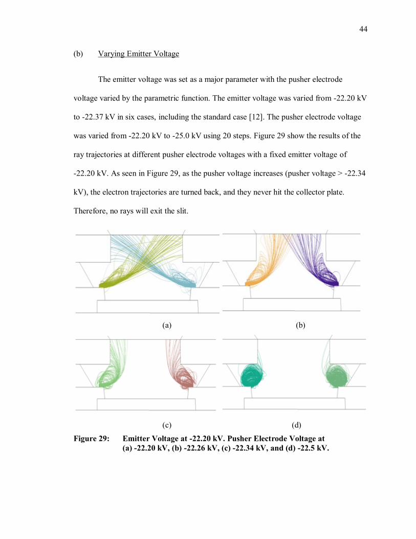
44
(b) Varying Emitter Voltage
The emitter voltage was set as a major parameter with the pusher electrode
voltage varied by the parametric function. The emitter voltage was varied from -22.20 kV
to -22.37 kV in six cases, including the standard case [12]. The pusher electrode voltage
was varied from -22.20 kV to -25.0 kV using 20 steps. Figure 29 show the results of the
ray trajectories at different pusher electrode voltages with a fixed emitter voltage of
-22.20 kV. As seen in Figure 29, as the pusher voltage increases (pusher voltage > -22.34
kV), the electron trajectories are turned back, and they never hit the collector plate.
Therefore, no rays will exit the slit.
(a) (b)
(c) (d)
Figure 29: Emitter Voltage at -22.20 kV. Pusher Electrode Voltage at
(a) -22.20 kV, (b) -22.26 kV, (c) -22.34 kV, and (d) -22.5 kV.

45
Collector Current Analysis
A diagnostic was placed at the collector to measure the number of rays that will
hit the collector. In Figure 30, a plot of the pusher electrode voltage vs. the rate of Iout/Iin
at different emitter voltages is presented. The voltage sensitivity (ΔV) was calculated and
the best case results are presented in Table 4.2. In this case, the best case corresponds to
the emitter voltage of -22.37 kV with a ΔV = 157.9. This case also guarantees 98% of the
rays exit the slit.
Figure 30: Pusher electrode voltage vs. current ratio.
Table 4.2: Voltage sensitivity analysis results for variations in the emitter
voltage.
Emitter voltage
(kV)
Maximum current
out (%)
ΔV (V)
-22.26 91.1% 63.15
-22.29 97.2% 78.95
-22.30 97.8% 94.74
-22.31 97.2% 126.3
-22.37 98.3% 157.9

46
(c) Varying the Geometry
In this section, the simulation results are from the variation of the geometry of the
pusher electrode; the simulations shown in Section (a) and (b) were repeated for each
geometry. The pusher electrode has a thickness of 0.9795 µm from the reference model
studied in [12]. This thickness was modified to its maximum and minimum to study the
device sensitivity due to changing the geometry/dimensions. The simulations are
performed for two different pusher electrode thicknesses: geometry (1) corresponds to a
thickness of 1.70 µm and geometry (2) corresponds to a thickness of 0.4475 µm. Some
examples of these results are presented in this section. The rest of the results are
presented in Appendix A. Figure 31 and Figure 33 correspond to results using a pusher
electrode thickness of 1.70 µm with a fixed pusher electrode voltage and a fixed emitter
voltage, respectively. Figure 35 and Figure 37 correspond to the results of using a pusher
electrode thickness of 0.4475 µm with a fixed pusher electrode voltage and a fixed
emitter voltage, respectively. For each case, the extracted current ratio is plotted in Figure
32, Figure 34, Figure 36, and Figure 38. The sensitivity tables are also shown in Table
4.3, Table 4.4, Table 4.5, and Table 4.6. These results clearly show an improvement in
the extracted current by moving the pusher electrode closer (vertically) to the emitter.
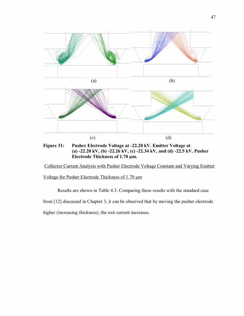
47
(a) (b)
(c) (d)
Figure 31: Pusher Electrode Voltage at -22.20 kV. Emitter Voltage at
(a) -22.20 kV, (b) -22.26 kV, (c) -22.34 kV, and (d) -22.5 kV. Pusher
Electrode Thickness of 1.70 µm.
Collector Current Analysis with Pusher Electrode Voltage Constant and Varying Emitter
Voltage for Pusher Electrode Thickness of 1.70 µm
Results are shown in Table 4.3. Comparing these results with the standard case
from [12] discussed in Chapter 3, it can be observed that by moving the pusher electrode
higher (increasing thickness), the exit current increases.

48
Figure 32: Emitter voltage vs. current ratio at different pusher electrode
voltages.
Table 4.3: Voltage sensitivity analysis results for variations in the pusher
electrode voltage with a pusher electrode thickness of 1.70 µm.
Pusher electrode voltage (kV) Maximum current out (%) ΔV (V)
-22.20 95.3% 79
-22.26 96.3% 126
-22.29 96.8% 189
-22.30 96.8% 222
-22.31 97.4% 173
-22.37 95.7% 190

49
(a) (b)
(c) (d)
Figure 33: Emitter Voltage at -22.20 kV. Pusher Electrode Voltage at
(a) -22.20 kV, (b) -22.26 kV, (c) -22.34 kV, and (d) -22.5 kV. Pusher
Electrode Thickness of 1.70 µm.
Collector Current Analysis with Emitter Voltage Constant and Varying Pusher Electrode
Voltage for a Pusher Electrode Thickness of 1.70 µm
Results are shown in Table 4.4. Comparing these results with the standard case
from [12] discussed in Chapter 3, it can be observed that by moving the pusher electrode
higher (increasing thickness), the exit current is increased. As observed in previous
results, for pusher electrode voltages greater than -22.34 kV, the rays will not exit the slit.

50
Figure 34: Pusher electrode voltage vs. current ratio at different emitter
voltages.
Table 4.4: Voltage sensitivity analysis results for variations in the emitter voltage
with a pusher electrode thickness of 1.7 µm.
Emitter voltage (kV) Maximum current out (%) ΔV (V)
-22.26 92.1% 113
-22.29 95.3% 90
-22.30 95.8% 90
-22.31 96.3% 90
-22.37 96.3% 110.5

51
(a) (b)
(c) (d)
Figure 35: Pusher Electrode Voltage at -22.20 kV. Emitter Voltage at
(a) -22.20 kV, (b) -22.26 kV, (c) -22.34 kV, and (d) -22.5 kV.
Collector Current Analysis with Pusher Electrode Voltage Constant and Varying Emitter
Voltage for a Pusher Electrode Thickness of 0.4475 µm
The results for ΔV are presented in Table 4.5. Comparing these results with the
standard case from [12] discussed in Chapter 3, it can be observed that by lowering
(decreasing thickness) the pusher electrode, the amount of current out is improved just for
few cases. Therefore, this change is not the most effective.

52
Figure 36: Emitter voltage vs. current ratio at different pusher electrode
voltages.
Table 4.5: Voltage sensitivity analysis results for variations in the pusher
electrode voltage with a pusher electrode thickness of 0.4475 µm.
Pusher electrode voltage (kV) Maximum current out (%) ΔV (V)
-22.31 92.2% 80
-22.37 98.9% 95

53
(a) (b)
(c) (d)
Figure 37: Emitter Voltage at -22.20 kV. Pusher Electrode Voltage at
(a) -22.20 kV, (b) -22.26 kV, (c) -22.34 kV, and (d) -22.5 kV.
Collector Current Analysis with Emitter Voltage Constant and Varying Pusher Electrode
Voltage for a Pusher Electrode Thickness of 0.4475 µm
The results for ΔV are presented in Table 4.6. The same results are observed as
previous case. It can be observed that by lowering (decreasing thickness) the pusher
electrode, the amount of current out is improved just for few cases. Therefore, this
approach is also not the most effective.

54
Figure 38: Pusher electrode voltage vs. current ratio at different emitter
voltages.
Table 4.6: Voltage sensitivity analysis results for variations in the emitter voltage
with a pusher electrode thickness of 0.4475 µm.
Emitter voltage (kV) Maximum current out (%) ΔV (V)
-22.29 97.2% 95
-22.30 97.8% 110.5
-22.31 96.1% 130
-22.37 98.9% 200
4.5 Summary of Results
The tests presented in this chapter are important for design considerations. It is
useful to know the sensitivity of the field emitters in terms of voltage and location
parameters. Since some of the field emitters will not operate at the same voltage, this
technique is used to study a range of voltages (ΔV) that still guarantees adequate
operation. Similarly, this range can also be studied by changing the location of the pusher
electrode. From the sensitivity analysis, it was found that the maximum current out was
55
obtained by setting the pusher electrode and the emitter electrode to -22.37 kV, and the
thickness of the pusher electrode remained the same at 0.85 µm (reference case [12]).
The maximum current (maximum number of rays exit the slit) obtained was of 98.3%
with a ΔV range of 160 to190 V. At the beginning of this research, these results were
going to be used as input parameters for the VORPAL simulations; however, this was not
completed, and the VORPAL model was developed based on previous work completed in
ICEPIC [12]. Therefore, the results presented were left as a future activity for device
modeling and fabrication.

56
CHAPTER FIVE: VORPAL SIMULATION SETUP
5.1 Overview
The primary research activity of this dissertation has been in the simulation of the
new magnetron device using the modulated, addressable cathode concept. This chapter
will give an overview of the particle-in-cell (PIC) code VORPAL used in this research; in
addition, a discussion of the basic simulation aspects including the finite difference time
domain (FDTD) technique, boundary conditions, the Dey-Mittra cut-cell algorithm, and
the simulation setup will be discussed. Finally, the modeling procedures for the 2-D, ten-
cavity, rising sun magnetron will be presented.
5.2 Software
Computational techniques are a critical component of the research and design
process, which is important for electromagnetic engineering systems where solutions to
Maxwell‟s equations in complex geometries are difficult to solve. Simulation provides
many benefits such as numerous diagnostic capabilities and a controlled environment
[75]. This work studies the performance of the rising sun magnetron with the faceted-
shaped cathode using the particle-in-cell (PIC) code VORPAL 5.2 [22, 76, 77]. Other
PIC codes have been used before to study magnetrons including QUICKSILVER [78],
MAGIC [13, 24, 26, 29, 31, 35, 37, 47, 58, 79, 80], ICEPIC [12, 71], and others [24, 36,
41-44, 81]. This work dedicates a section of the study to compare results using two PIC

57
codes: ICEPIC (prior work) [12] and VORPAL. The rest of the simulation work has been
carried out using only the PIC code VORPAL.
VORPAL is a particle-in-cell (PIC) code developed by Tech-X Corporation [22,
76] that can model complex electromagnetic structures and is capable of simulating one,
two, or three dimensions. VORPAL is designed to run as both a serial code for single-
processor workstations and as a parallel code for systems that support Message Passing
Interface (MPI). Most of the simulations in this research were run using a single core
processor workstation. Although the simulations completed in this research are in 2D, the
concepts explained for the numerical methods used in VORPAL are described for general
3D models.
5.3 Finite Difference Time Domain (FDTD) Technique
VORPAL offers a unique combination of physical models to cover the entire
range of plasma simulation problems. VORPAL uses the finite difference-time domain
(FDTD) method to solve Maxwell‟s equations and includes an advanced technique
known as cut-cell boundaries to allow accurate representation of curved geometries
within a Cartesian grid: the Dey-Mittra algorithm [18, 82, 83].
The electromagnetic fields are solved by using the FDTD method constructed by
Yee [84]. The FDTD method solves the curl equations 5.1 and 5.2, supposing divergence
free initial conditions for the field strengths [85].
o
t
HE
(5.1)
o
t
EH J
(5.2)

58
where E and H are the electric and magnetic field vectors, µo and εo are the
permeability and permittivity of free space, and J is the current density and is set to:
J E (5.3)
where is the conductivity.
Under the Cartesian coordinate system, these can be further expanded as:
1 yx z
o
EH E
t y z
(5.4)
1y x z
o
H E E
t z x
(5.5)
1 y xz
o
E EH
t x y
(5.6)
1 yx zx
o
HE HE
t y z
(5.7)
1y x zy
o
E H HE
t z x
(5.8)
1 y xzz
o
H HEE
t x y
(5.9)
In Yee‟s scheme [84], the model is first divided into many small cubes. For
simplicity, the cubes are assumed to be the same size. The edges of each cube will form
the three-dimensional space grid. Introducing the notation:
( , , ) , , ,n
x i j k xE E i x j y k z n t (5.10)
and so on for Ey, Ez, Hx, Hy, and Hz components, where Δt is the time increment and Δx,
Δy, and Δz are the spatial discretization. Reducing 5.10 to a 2D grid model:
( , ) , ,n
x i j xE E i x j y n t (5.11)

59
and so on for Ey, and Hz components, where Δt is the time increment and Δx, and Δy are
the spatial discretization, respectively.
The method starts with the definition of a generally rectangular mesh for the
electric field and another staggered grid for the magnetic field in the computational
domain. The building blocks of this mesh are the Yee-cells. The basic setup of the Yee
electromagnetic field is illustrated in Figure 39. In this setup, electric fields are located on
the edges of grid cells, and magnetic fields are located on the faces of the cell surfaces.
Figure 39: Yee model for placing fields on the grid [86].
Figure 40 illustrates the basic flow of implementing Yee‟s FDTD scheme on a
computer, following these steps: (1) the electric field and magnetic field components are
initialized to zero as well as all the sources, (2) the new electric field component values
are computed at interior cells, followed by computing the electric field component values
at the boundary, (3) the new magnetic field component values are computed, (4) if the
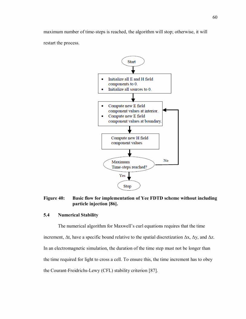
60
maximum number of time-steps is reached, the algorithm will stop; otherwise, it will
restart the process.
Figure 40: Basic flow for implementation of Yee FDTD scheme without including
particle injection [86].
5.4 Numerical Stability
The numerical algorithm for Maxwell‟s curl equations requires that the time
increment, Δt, have a specific bound relative to the spatial discretization Δx, Δy, and Δz.
In an electromagnetic simulation, the duration of the time step must not be longer than
the time required for light to cross a cell. To ensure this, the time increment has to obey
the Courant-Freidrichs-Lewy (CFL) stability criterion [87].

61
2 2 2
1
1 1 1t
cx y z
(5.12)
where c is:
1
o o
c
(5.13)
In 2D the CFL stability criterion is reduced to:
2 2
1
1 1t
cx y
(5.14)
If the Courant condition is not followed, the simulation will not be stable [18, 75].
VORPAL uses a fraction of the Courant time step for which the simulation will be
stable when using the Dey-Mittra boundary algorithm with the Yee method. For example,
if this fraction is equal to 0.25, then the time step for the simulation must be 25% of the
Courant time step [18]. Note that for this research the electron source is modulated
temporally at the operating frequency of the magnetron. To ensure that this modulation is
consistent over time steps, the time step size was set to an integer fraction of the
magnetron RF period while still satisfying the stability condition.
5.5 Boundary Conditions
In a typical simulation, boundary conditions are set at selected surfaces, and they
may be set throughout a volume. In VORPAL, they can be specified as [18]:
Wave launcher to specify the characteristics of a wave.

62
Conductor to specify a perfectly conducting metal wall. Perfect conductors in
VORPAL are imagined to have an infinite supply of electrons to cancel any charge
buildup.
If an electromagnetic boundary condition is not specified explicitly, the default
value is a conductor boundary condition. Simulations can deal with curved boundaries;
for this, VORPAL implements either the stair-step approximation of the curved surface
or the Dey-Mittra cut cell method.
5.6 Dey-Mittra Cut Cell Algorithm
Curved boundaries are often modeled with stair-step boundaries, which are
known to be first order accurate [88]. To overcome this limitation, VORPAL implements
the Dey-Mittra [89] cut-cell boundary algorithm, which is known to be second order
accurate [82, 83].
The Dey-Mittra algorithm uses a loop integral along the edges of each cell face by
using the Faraday update of the magnetic field on the standard Yee mesh. The loop
integral is limited to the edges that are completely or partially inside the boundary if the
cell is cut by the boundary. If the edges are not completely inside the boundary, their
lengths are reduced by the suitable amount. The area used in the integral is also reduced
by the area inside the boundary [83]. The time step must obey the Courant condition for
the smallest cut cell on the boundary to maintain stability. To keep the time step at a
reasonable value, VORPAL introduces an input parameter, which gives the fraction of
the Courant step that is allowed. Then, the code checks all the cut cells to see if they
would be stable for the first time step. If the cut cells are not stable, they will be discarded
[83].
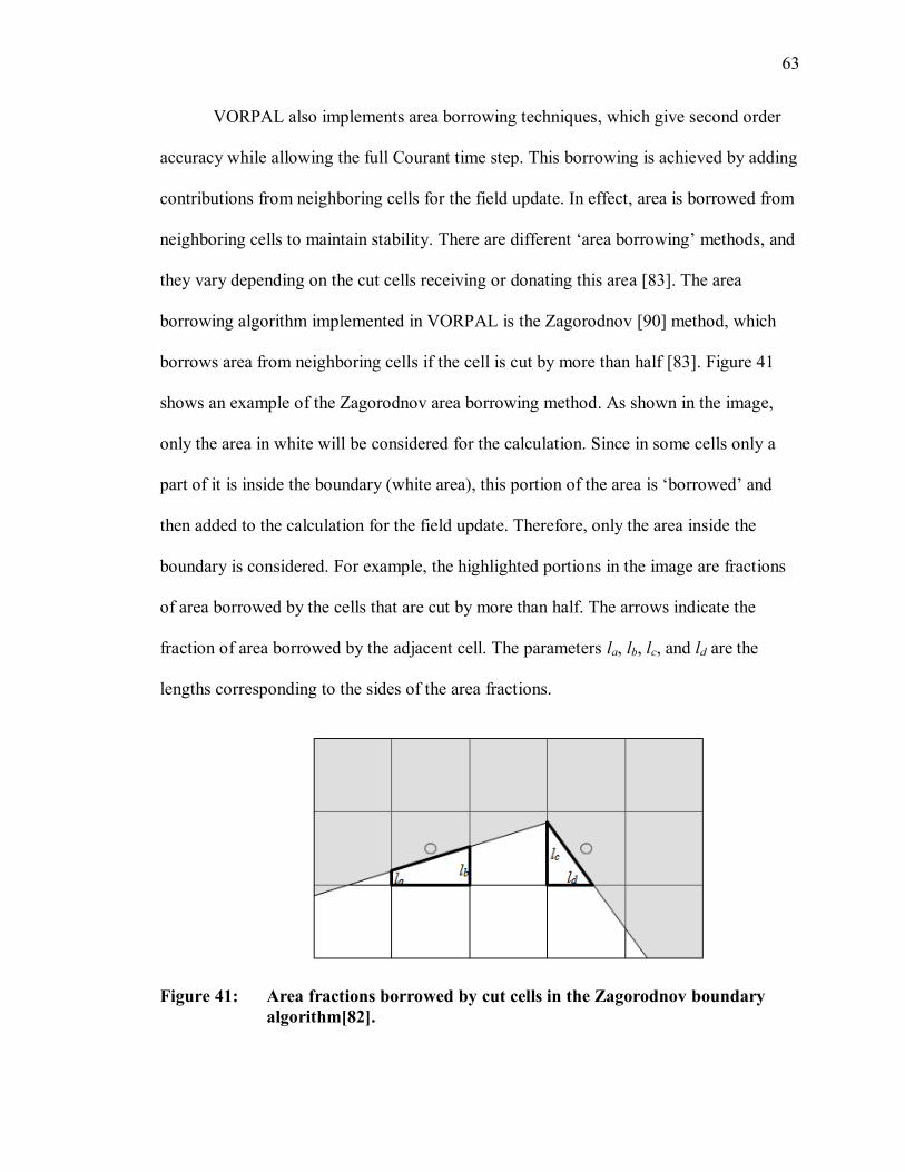
63
VORPAL also implements area borrowing techniques, which give second order
accuracy while allowing the full Courant time step. This borrowing is achieved by adding
contributions from neighboring cells for the field update. In effect, area is borrowed from
neighboring cells to maintain stability. There are different „area borrowing‟ methods, and
they vary depending on the cut cells receiving or donating this area [83]. The area
borrowing algorithm implemented in VORPAL is the Zagorodnov [90] method, which
borrows area from neighboring cells if the cell is cut by more than half [83]. Figure 41
shows an example of the Zagorodnov area borrowing method. As shown in the image,
only the area in white will be considered for the calculation. Since in some cells only a
part of it is inside the boundary (white area), this portion of the area is „borrowed‟ and
then added to the calculation for the field update. Therefore, only the area inside the
boundary is considered. For example, the highlighted portions in the image are fractions
of area borrowed by the cells that are cut by more than half. The arrows indicate the
fraction of area borrowed by the adjacent cell. The parameters la, lb, lc, and ld are the
lengths corresponding to the sides of the area fractions.
Figure 41: Area fractions borrowed by cut cells in the Zagorodnov boundary
algorithm[82].
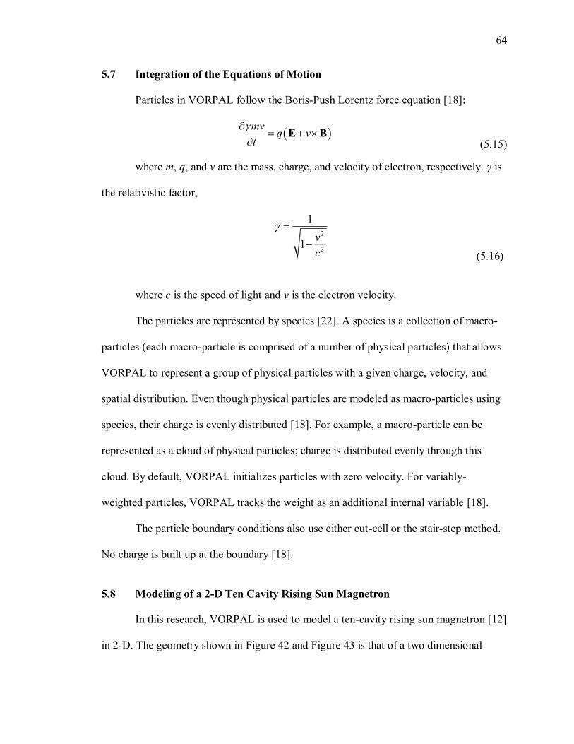
64
5.7 Integration of the Equations of Motion
Particles in VORPAL follow the Boris-Push Lorentz force equation [18]:
mvq v
t
E B
(5.15)
where m, q, and v are the mass, charge, and velocity of electron, respectively. γ is
the relativistic factor,
2
2
1
1v
c
(5.16)
where c is the speed of light and v is the electron velocity.
The particles are represented by species [22]. A species is a collection of macro-
particles (each macro-particle is comprised of a number of physical particles) that allows
VORPAL to represent a group of physical particles with a given charge, velocity, and
spatial distribution. Even though physical particles are modeled as macro-particles using
species, their charge is evenly distributed [18]. For example, a macro-particle can be
represented as a cloud of physical particles; charge is distributed evenly through this
cloud. By default, VORPAL initializes particles with zero velocity. For variably-
weighted particles, VORPAL tracks the weight as an additional internal variable [18].
The particle boundary conditions also use either cut-cell or the stair-step method.
No charge is built up at the boundary [18].
5.8 Modeling of a 2-D Ten Cavity Rising Sun Magnetron
In this research, VORPAL is used to model a ten-cavity rising sun magnetron [12]
in 2-D. The geometry shown in Figure 42 and Figure 43 is that of a two dimensional

65
rising sun magnetron with two cathode geometries: cylindrical and faceted. As seen in
Figure 42 and Table 5.1, the radius of the cylindrical cathode is 1.0 cm, and the inner
radius of the anode is 2.24 cm. Long cavities have an outer radius of 10.0 cm and opening
angle of 10◦. Short cavities have an outer radius of 6.0 cm and opening angle of 10
◦. The
faceted cathode with five facets has a facet width of 1.18 cm and a vertex angle
orientation of 3π/2 radians. The vertex angle (see Figure 43) is a parameter that can be
varied in the simulation, allowing cathode rotation. The ten-sided cathode has a facet
width of 0.618 cm. These geometrical properties control the spectrum and, thus, the
operating frequency of the cavity, which is 960 MHz for the cylindrical cathode and 957
MHz for the faceted cathodes.
One long cavity is loaded with a damping parameter, used in VORPAL, with a
value of Nu_loading = 200.0 x 10⁶ /s to model a coupler to the magnetron. The cavity is
loaded as if its volume were resistive (e.g., there is effectively an ohmic current J= E,
where is tuned to give the desired quality factor Q). This loading parameter may be
used to tune the quality factor, Q, of the magnetron, which is proportional to 1/
Nu_loading.

66
Figure 42: Cylindrical cathode used in VORPAL simulations.
Figure 43: Five-sided faceted cathode used in VORPAL simulations.

67
Figure 44: Ten-sided faceted cathode used in VORPAL simulations.
Table 5.1: Rising sun magnetron dimensions for cylindrical, five and ten-
sided faceted cathodes.
5.9 Simulation Setup and Procedures
For this research, a typical VORPAL simulation is set up with a grid of 102x102
cells with a length of 20.4 cm in the x-direction and 20.4 cm in the y-direction. However,
for the 10-sided case, the grid must be increased to 202x202 to account for the needed
spatial resolution of the finer facets and the emitter sections. The time step size is
typically 2.3e-12 s, and the simulation total run time is 600 ns. For the modulated current
Cathode
radius
(cm)
Anode
radius
(cm)
Facet width (cm) Small cavity
outer radius
(cm)
Large
cavity outer
radius (cm)
Cavity
angle
(degrees) Pentagon Decagon
1.0 2.24 1.18 0.618 6.0 10.0 10
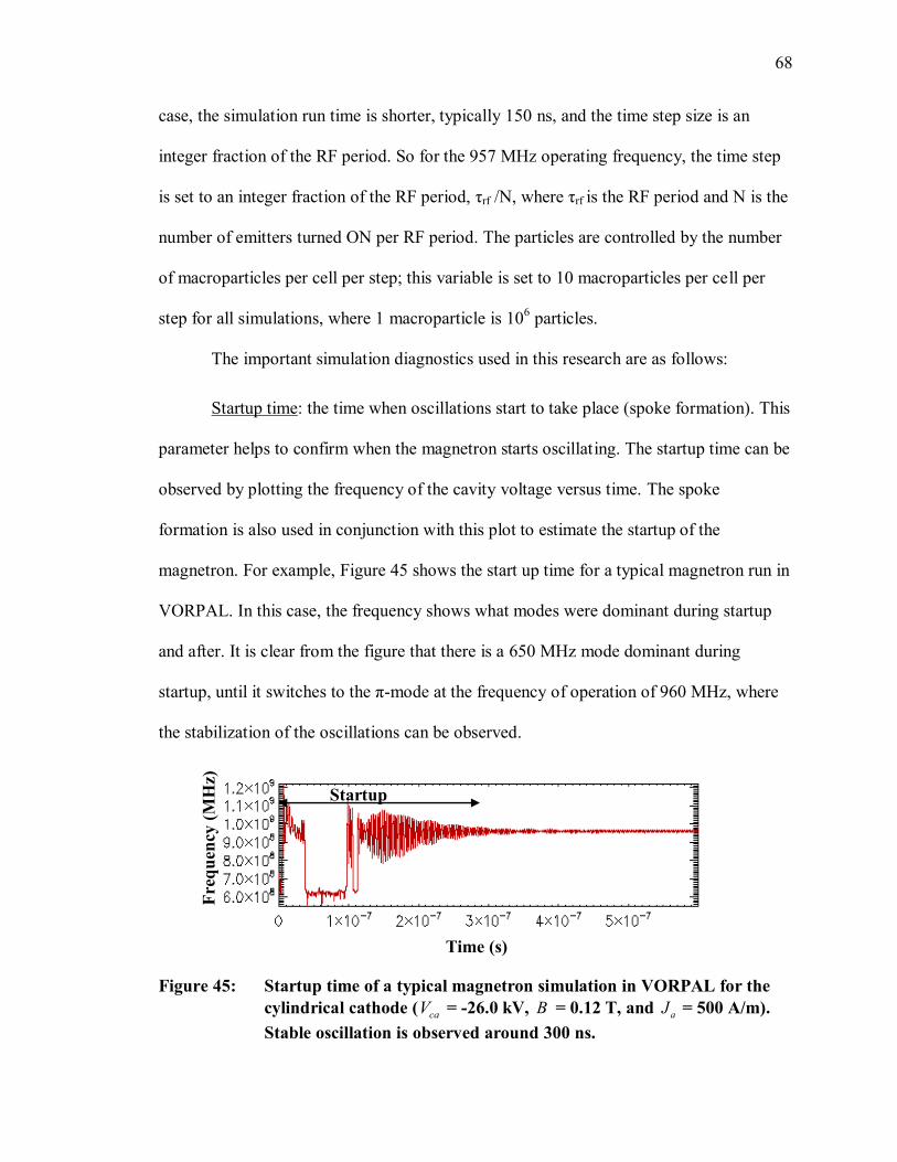
68
case, the simulation run time is shorter, typically 150 ns, and the time step size is an
integer fraction of the RF period. So for the 957 MHz operating frequency, the time step
is set to an integer fraction of the RF period, τrf /N, where τrf is the RF period and N is the
number of emitters turned ON per RF period. The particles are controlled by the number
of macroparticles per cell per step; this variable is set to 10 macroparticles per cell per
step for all simulations, where 1 macroparticle is 106 particles.
The important simulation diagnostics used in this research are as follows:
Startup time: the time when oscillations start to take place (spoke formation). This
parameter helps to confirm when the magnetron starts oscillating. The startup time can be
observed by plotting the frequency of the cavity voltage versus time. The spoke
formation is also used in conjunction with this plot to estimate the startup of the
magnetron. For example, Figure 45 shows the start up time for a typical magnetron run in
VORPAL. In this case, the frequency shows what modes were dominant during startup
and after. It is clear from the figure that there is a 650 MHz mode dominant during
startup, until it switches to the π-mode at the frequency of operation of 960 MHz, where
the stabilization of the oscillations can be observed.
Figure 45: Startup time of a typical magnetron simulation in VORPAL for the
cylindrical cathode ( caV = -26.0 kV, B = 0.12 T, and aJ = 500 A/m).
Stable oscillation is observed around 300 ns.
Time (s)
Fre
qu
ency
(M
Hz)
Startup

69
Total Emitted Current: This diagnostic measures the total emitted average current
of the device. Because this is a 2-D simulation, a linear current density (A/m) is used for
this purpose. In this simulation model, the anode structure is set as a collector; the
magnetic field is set to zero; and the simulation is run for the total run period, typically
600 ns for the reference case and 150 ns for the current modulated case. Particles are
collected on the anode, and then the average emitted current is determined. This
diagnostic is used to look for timing errors in the modulation simulations and to make
certain that the average emitted current is correct. Figure 46 shows an example of the
average linear current density versus time for the cylindrical cathode geometry. This is a
typical VORPAL simulation with an emitted linear current density of 500 A/m and a total
simulation run of 600 ns.
Figure 46: Linear current density vs. time for the cylindrical cathode, typical
VORPAL simulation with B field = 0.
Anode Current: This diagnostic measures the total average anode current while
the device is in operation. It is used to determine startup of oscillation and to look for
stability issues in the oscillations. Note that the anode current density does not become
completely stable until after 350 ns. It is also useful for calculating the input power
density of the device. For example, Figure 47 shows a typical VORPAL simulation result
of the anode linear current density for the cylindrical cathode during operation; this value
Time (s) C
urr
ent
Den
sity
(A
/m)
7
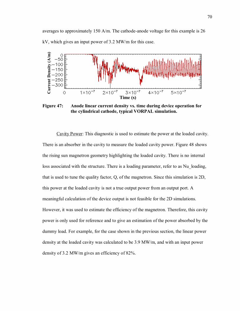
70
averages to approximately 150 A/m. The cathode-anode voltage for this example is 26
kV, which gives an input power of 3.2 MW/m for this case.
Figure 47: Anode linear current density vs. time during device operation for
the cylindrical cathode, typical VORPAL simulation.
Cavity Power: This diagnostic is used to estimate the power at the loaded cavity.
There is an absorber in the cavity to measure the loaded cavity power. Figure 48 shows
the rising sun magnetron geometry highlighting the loaded cavity. There is no internal
loss associated with the structure. There is a loading parameter, refer to as Nu_loading,
that is used to tune the quality factor, Q, of the magnetron. Since this simulation is 2D,
this power at the loaded cavity is not a true output power from an output port. A
meaningful calculation of the device output is not feasible for the 2D simulations.
However, it was used to estimate the efficiency of the magnetron. Therefore, this cavity
power is only used for reference and to give an estimation of the power absorbed by the
dummy load. For example, for the case shown in the previous section, the linear power
density at the loaded cavity was calculated to be 3.9 MW/m, and with an input power
density of 3.2 MW/m gives an efficiency of 82%.
Time (s) C
urr
ent
Den
sity
(A
/m)

71
Figure 48: Rising sun magnetron cavity power diagnostic location.
Phase: This diagnostic will help to determine at what relative phase the magnetron
is oscillating. Visually, it can be determined by the spoke locations, and the
corresponding time step can be found in the simulation. Figure 49 shows an example of
the magnetron oscillations (spoke formation) with a selected reference cavity.
Measurement of the phase will also be performed by using a correlation between a
reference case and the phase changed case to calculate the phase difference from the RF
Bz field.
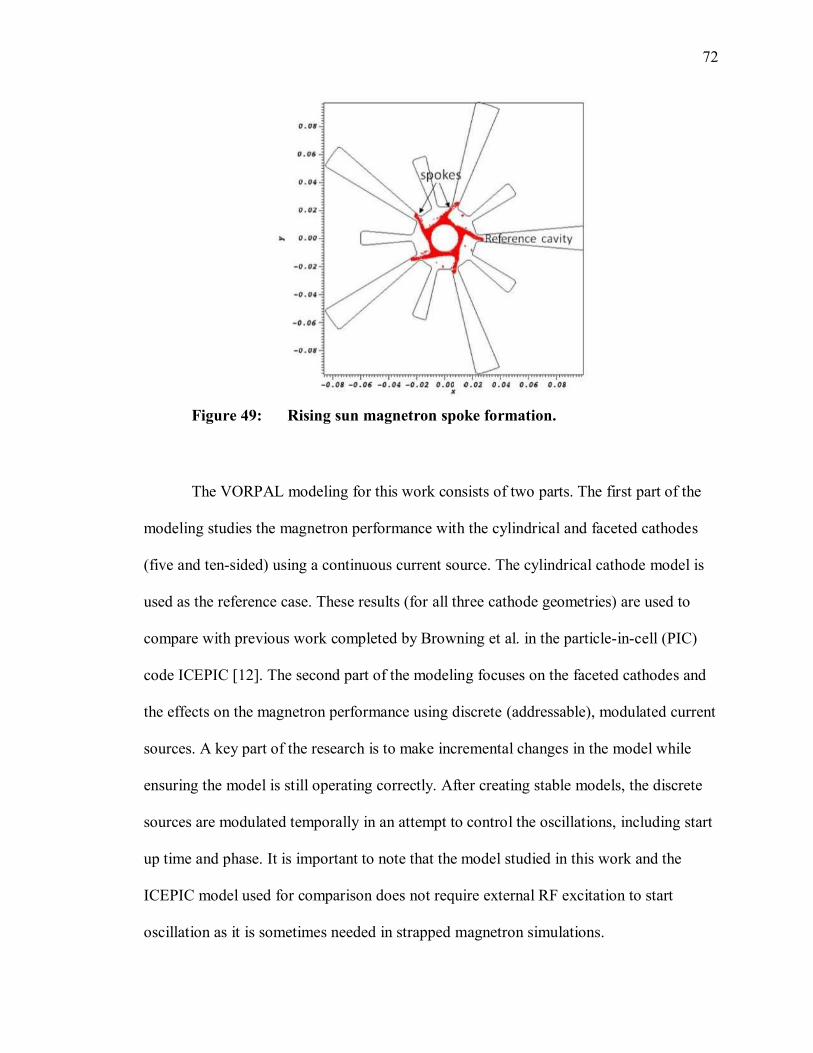
72
Figure 49: Rising sun magnetron spoke formation.
The VORPAL modeling for this work consists of two parts. The first part of the
modeling studies the magnetron performance with the cylindrical and faceted cathodes
(five and ten-sided) using a continuous current source. The cylindrical cathode model is
used as the reference case. These results (for all three cathode geometries) are used to
compare with previous work completed by Browning et al. in the particle-in-cell (PIC)
code ICEPIC [12]. The second part of the modeling focuses on the faceted cathodes and
the effects on the magnetron performance using discrete (addressable), modulated current
sources. A key part of the research is to make incremental changes in the model while
ensuring the model is still operating correctly. After creating stable models, the discrete
sources are modulated temporally in an attempt to control the oscillations, including start
up time and phase. It is important to note that the model studied in this work and the
ICEPIC model used for comparison does not require external RF excitation to start
oscillation as it is sometimes needed in strapped magnetron simulations.

73
5.10 Rising Sun Magnetron Model with a Continuous Current Source
There are four run types developed for the cathode geometries. These runs are
completed to study the device operation. They consist of (a) the mode spectrum: to study
the possible frequencies where the device will have oscillating modes; (b) calibration of
the π-mode and the quality factor: the simulation can be tuned to the desired frequency of
operation and a plot of the RF B field can be obtained to check for the π mode; (c)
calibrating the DC voltage: this run is used to determine the voltage parameter that will
support the desired operating mode; and (d) the run with particles: after the model is
completely calibrated, a complete run with particles is performed, and then all the
diagnostics can be checked. These four simulation runs are discussed in more detail as
follows:
The Mode Spectrum:
This simulation is used to predict the magnetron operating frequency. The Fast
Fourier Transform (FFT) of the voltage at one of the cavities is analyzed to find the
frequency of operation. Figure 50 shows the mode spectrum for a typical run in
VORPAL. The Fast Fourier Transform (FFT) of the voltage across the cavity is plotted
versus frequency (in Hz). This result indicates that the magnetron is expected to have
oscillating modes near 650 MHz and 960 MHz.
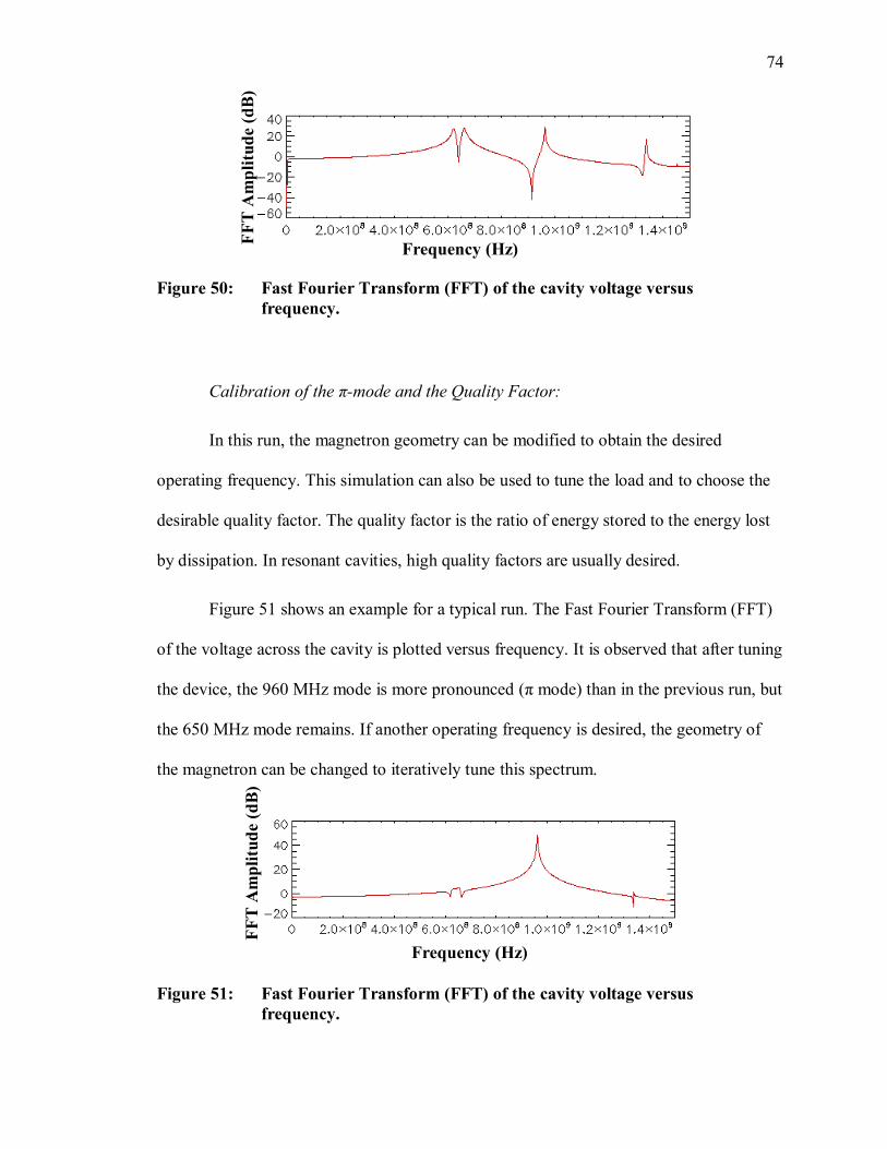
74
Figure 50: Fast Fourier Transform (FFT) of the cavity voltage versus
frequency.
Calibration of the π-mode and the Quality Factor:
In this run, the magnetron geometry can be modified to obtain the desired
operating frequency. This simulation can also be used to tune the load and to choose the
desirable quality factor. The quality factor is the ratio of energy stored to the energy lost
by dissipation. In resonant cavities, high quality factors are usually desired.
Figure 51 shows an example for a typical run. The Fast Fourier Transform (FFT)
of the voltage across the cavity is plotted versus frequency. It is observed that after tuning
the device, the 960 MHz mode is more pronounced (π mode) than in the previous run, but
the 650 MHz mode remains. If another operating frequency is desired, the geometry of
the magnetron can be changed to iteratively tune this spectrum.
Figure 51: Fast Fourier Transform (FFT) of the cavity voltage versus
frequency.
Frequency (Hz) F
FT
Am
pli
tud
e (d
B)
Frequency (Hz)
FF
T A
mp
litu
de (
dB
)

75
Another parameter that may be tuned is the magnetron quality factor, Q. It is
expected that 1/Q will vary as Nu_loading (loading cavity factor), but it is also possible
to determine the Q using VORPAL. Using a short no-particle run, the decay of the cavity
voltage signal (Figure 52a) and its amplitude (Figure52b) can be used to determine Q by
using the following equation [91, 92]:
2
( ) ( )
tQ
V t V t eo
(5.17)
where V(t) is the cavity voltage, and ω is the angular resonant frequency (ω=2πf).
Therefore, Q can be expressed as:
1
2
1
2
( )ln
( )
t
QV t
V t
(5.18)
where Δt = t2-t1
For example, from Figure 53(b) t1 = 0 ns and t2 = 20 ns, V(t1) = 2610 V and V(t2)
= 2250 V; Q is then calculated as
Q = (π)(0.96e9)(20e-9)ln-1
(2610/2250) = 406.
This Q is the same for all of the simulation work presented in this research.
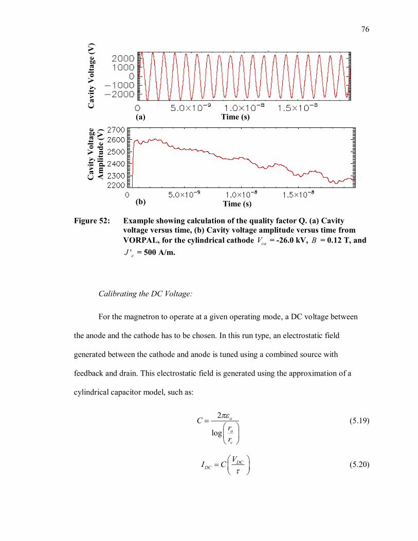
76
Figure 52: Example showing calculation of the quality factor Q. (a) Cavity
voltage versus time, (b) Cavity voltage amplitude versus time from
VORPAL, for the cylindrical cathode caV = -26.0 kV, B = 0.12 T, and
'eJ = 500 A/m.
Calibrating the DC Voltage:
For the magnetron to operate at a given operating mode, a DC voltage between
the anode and the cathode has to be chosen. In this run type, an electrostatic field
generated between the cathode and anode is tuned using a combined source with
feedback and drain. This electrostatic field is generated using the approximation of a
cylindrical capacitor model, such as:
2
log
o
a
c
Cr
r
(5.19)
DC
DC
VI C
(5.20)
(b)
Time (s)
Cavit
y V
olt
age
(V)
(a)
Time (s)
Cavit
y V
olt
age
Am
pli
tud
e (V
)
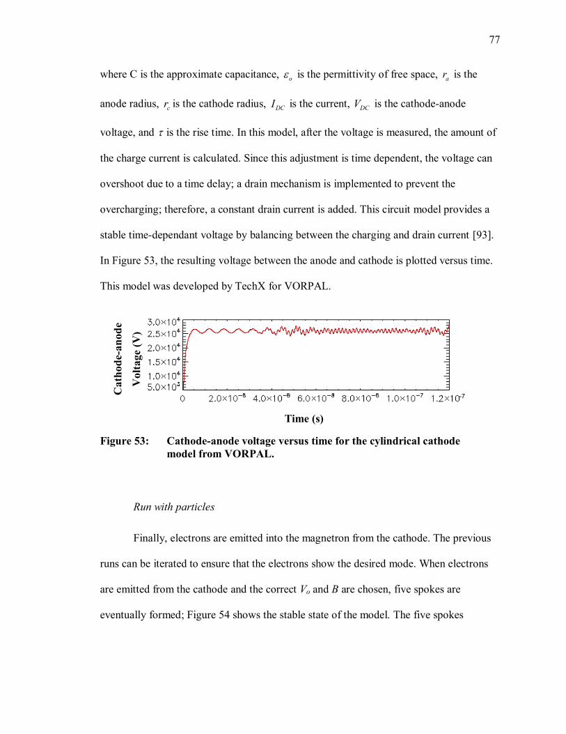
77
where C is the approximate capacitance, o is the permittivity of free space,
ar is the
anode radius, cr is the cathode radius,
DCI is the current, DCV is the cathode-anode
voltage, and is the rise time. In this model, after the voltage is measured, the amount of
the charge current is calculated. Since this adjustment is time dependent, the voltage can
overshoot due to a time delay; a drain mechanism is implemented to prevent the
overcharging; therefore, a constant drain current is added. This circuit model provides a
stable time-dependant voltage by balancing between the charging and drain current [93].
In Figure 53, the resulting voltage between the anode and cathode is plotted versus time.
This model was developed by TechX for VORPAL.
Figure 53: Cathode-anode voltage versus time for the cylindrical cathode
model from VORPAL.
Run with particles
Finally, electrons are emitted into the magnetron from the cathode. The previous
runs can be iterated to ensure that the electrons show the desired mode. When electrons
are emitted from the cathode and the correct Vo and B are chosen, five spokes are
eventually formed; Figure 54 shows the stable state of the model. The five spokes
Time (s)
Cath
od
e-an
od
e
Volt
age
(V)
-7
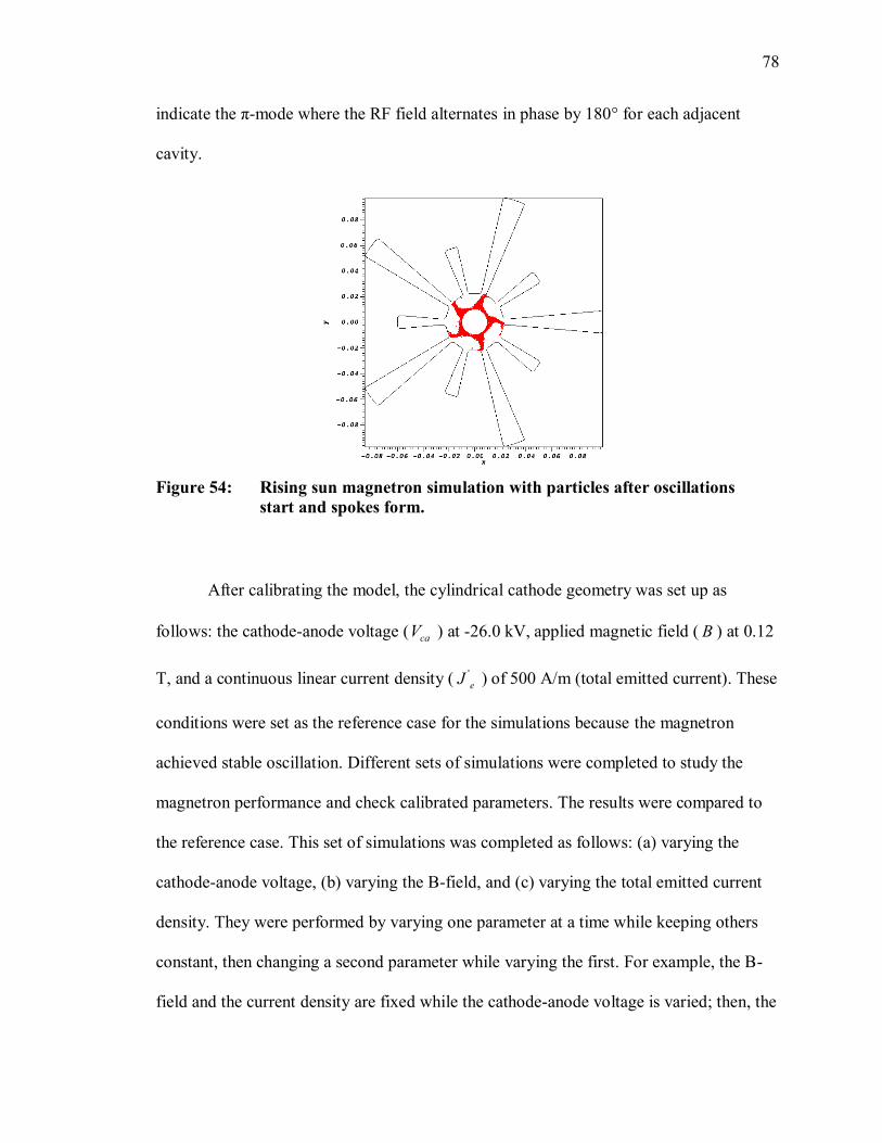
78
indicate the π-mode where the RF field alternates in phase by 180° for each adjacent
cavity.
Figure 54: Rising sun magnetron simulation with particles after oscillations
start and spokes form.
After calibrating the model, the cylindrical cathode geometry was set up as
follows: the cathode-anode voltage ( caV ) at -26.0 kV, applied magnetic field ( B ) at 0.12
T, and a continuous linear current density ( '
eJ ) of 500 A/m (total emitted current). These
conditions were set as the reference case for the simulations because the magnetron
achieved stable oscillation. Different sets of simulations were completed to study the
magnetron performance and check calibrated parameters. The results were compared to
the reference case. This set of simulations was completed as follows: (a) varying the
cathode-anode voltage, (b) varying the B-field, and (c) varying the total emitted current
density. They were performed by varying one parameter at a time while keeping others
constant, then changing a second parameter while varying the first. For example, the B-
field and the current density are fixed while the cathode-anode voltage is varied; then, the

79
B-field is changed while the voltage and the current density are fixed. Table 5.2
summarizes the completed simulations. These simulations were performed for model
calibration. Only the best results (most stable model) will be presented. The total emitted
current was varied from 125A/m to 1000 A/m, keeping the cathode-anode voltage
constant (reference case). The startup time for each current value was measured and
compared with the reference case.
In the case of the faceted cathodes, a similar procedure was followed. The set of
simulations for the five-sided cathode was completed as follows: (a) varying the cathode-
anode voltage, (b) varying the B-field, and (c) varying the anode current. From these
results, it was found that for this model a caV = -22.2 kV, B = 0.09 T, and 'eJ = 326 A/m
were the parameters that gave the most stable model for the faceted cathodes. These
simulations were used for model calibration and are shown in Table 5.2 and Table 5.3.
For the ten-sided cathode, these simulations were not all completed because this model
had better stability, and after investigating some of the parameters, it was easier to
determine that the most stable case was for caV = -22.2 kV, B = 0.09 T, and 'eJ = 326
A/m. The total emitted current density was also varied for the faceted geometries from
81.5 A/m to 652 A/m, keeping the cathode-anode voltage constant (reference case). The
startup time for each current value was measured and compared with the reference case.
These results are presented in Chapter 6.
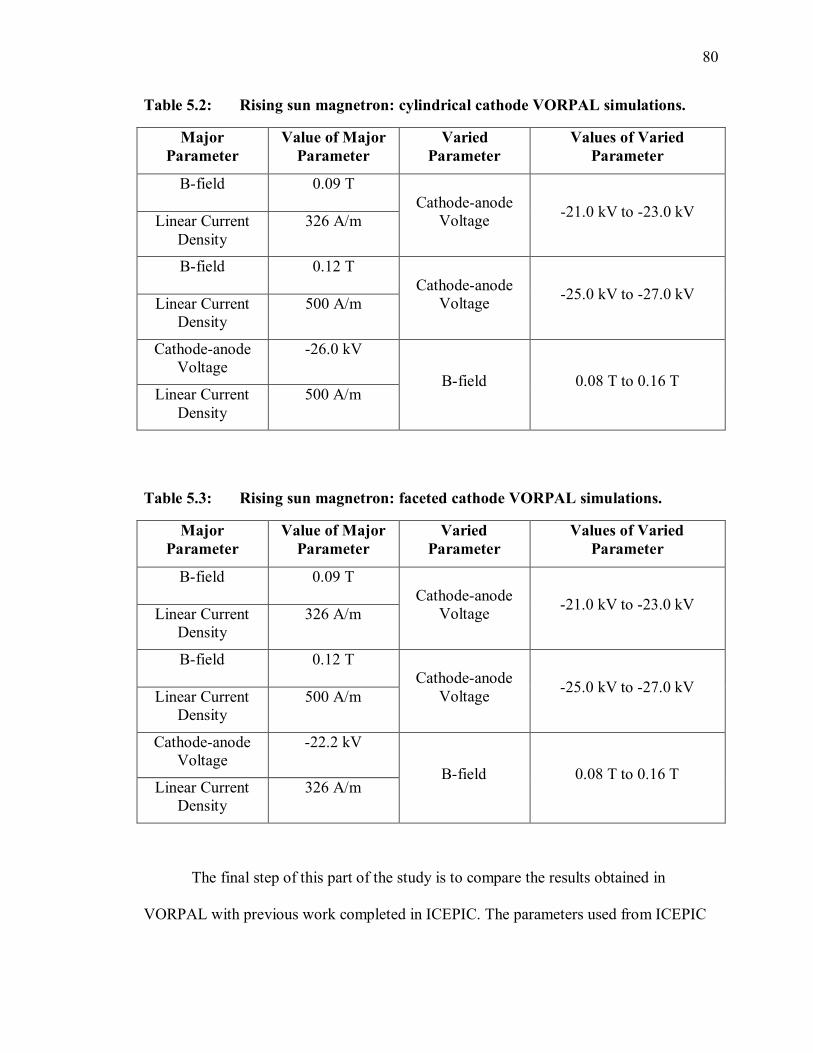
80
Table 5.2: Rising sun magnetron: cylindrical cathode VORPAL simulations.
Major
Parameter
Value of Major
Parameter
Varied
Parameter
Values of Varied
Parameter
B-field 0.09 T
Cathode-anode
Voltage -21.0 kV to -23.0 kV
Linear Current
Density
326 A/m
B-field 0.12 T
Cathode-anode
Voltage -25.0 kV to -27.0 kV
Linear Current
Density
500 A/m
Cathode-anode
Voltage
-26.0 kV
B-field 0.08 T to 0.16 T Linear Current
Density
500 A/m
Table 5.3: Rising sun magnetron: faceted cathode VORPAL simulations.
Major
Parameter
Value of Major
Parameter
Varied
Parameter
Values of Varied
Parameter
B-field 0.09 T
Cathode-anode
Voltage -21.0 kV to -23.0 kV
Linear Current
Density
326 A/m
B-field 0.12 T
Cathode-anode
Voltage -25.0 kV to -27.0 kV
Linear Current
Density
500 A/m
Cathode-anode
Voltage
-22.2 kV
B-field 0.08 T to 0.16 T Linear Current
Density
326 A/m
The final step of this part of the study is to compare the results obtained in
VORPAL with previous work completed in ICEPIC. The parameters used from ICEPIC
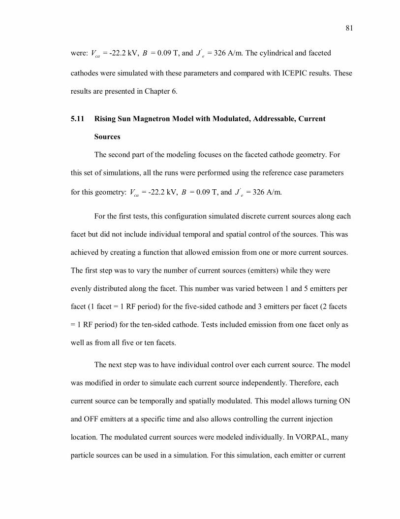
81
were: caV = -22.2 kV, B = 0.09 T, and '
eJ = 326 A/m. The cylindrical and faceted
cathodes were simulated with these parameters and compared with ICEPIC results. These
results are presented in Chapter 6.
5.11 Rising Sun Magnetron Model with Modulated, Addressable, Current
Sources
The second part of the modeling focuses on the faceted cathode geometry. For
this set of simulations, all the runs were performed using the reference case parameters
for this geometry: caV = -22.2 kV, B = 0.09 T, and '
eJ = 326 A/m.
For the first tests, this configuration simulated discrete current sources along each
facet but did not include individual temporal and spatial control of the sources. This was
achieved by creating a function that allowed emission from one or more current sources.
The first step was to vary the number of current sources (emitters) while they were
evenly distributed along the facet. This number was varied between 1 and 5 emitters per
facet (1 facet = 1 RF period) for the five-sided cathode and 3 emitters per facet (2 facets
= 1 RF period) for the ten-sided cathode. Tests included emission from one facet only as
well as from all five or ten facets.
The next step was to have individual control over each current source. The model
was modified in order to simulate each current source independently. Therefore, each
current source can be temporally and spatially modulated. This model allows turning ON
and OFF emitters at a specific time and also allows controlling the current injection
location. The modulated current sources were modeled individually. In VORPAL, many
particle sources can be used in a simulation. For this simulation, each emitter or current
82
source was modeled as a particle source in which a time of ON and OFF can be specified
as well as the location on the facet. The current sources were placed evenly distributed on
the facet with small gaps in between them. Figure 55 shows an example (concept) of the
application of this technique on the five-sided cathode. For simulation purposes, this case
shows the five-sided faceted cathode with 5 emitter elements per facet (25 emitter
elements total) (see Figure 55(a)). This particular example helps illustrate the application
of the current model. The current injection starts by first turning ON one emitter per
facet at a specific time while the others are turned OFF (emitters are represented by
arrows as indicated in Figure 55(a)). The emitters are turned ON in a sequence following
the electron spoke rotation direction, which is clockwise in this figure. The emitters are
turned ON and OFF in sequence and at the device oscillating frequency in order to
control the formation and location of the spokes versus time. Figure 55(a) shows how the
emitters are turned ON in a sequence. Figure 55(b) shows this behavior in more detail for
one of the facets, indicating the number of emitters that are turned ON and the number of
emitters turned OFF. This simulation was also repeated with a ten-sided faceted cathode
to compare the performance of the device due to a change in cathode geometries.

83
Figure 55: (a) Temporal and spatial modulation concept of the current
injection, showing electrons being injected in phase with spokes.
(b) Detailed view of one of the facets showing the ON and OFF
emitters.
The last step of this work is to demonstrate phase control. As described before,
the current sources can be turned ON and OFF in sequence to start oscillation. The
sequence can be changed versus time to change the spoke formation during oscillation.
Therefore, in the phase control simulation, the emitters can be turned ON and OFF at
different times.
After the additional simulation tests, it was found that the ten-sided faceted
cathode was more stable. Therefore, this geometry was used for the rest of the
simulations and for demonstrating the phase control technique. A dynamic phase shift of
180° was demonstrated. The phase shift was initiated at 88.40 ns, and then oscillations

84
later in time were compared to a reference point in time before the shift, which was
considered as phase 0°. The RF Bz field and spoke locations were used to analyze these
results. The signal was partitioned in two parts: the reference with no phase shift and the
phase shifted portion. The two curves were compared for different RF periods after the
phase shift to check how fast/slow the phase changed in time and achieved a steady state
at 180°. These results are presented in Chapter 7.
5.12 Additional Simulation Setups
During the research, various issues were encountered with the five-faceted
cathode and the modulation technique. The spokes did not completely form, and gaps or
blank spaces in the spokes were observed as well as instabilities in the anode current
density. In order to study these issues and improve performance and stability of the
magnetron, other simulation concepts were considered.
(a) The modulated, addressable current source model concept shown in Figure 55
was repeated, replacing the five-sided faceted cathode by a ten-sided faceted cathode. In
this case, each facet plate contained 3 emitters that can be addressed spatially and
modulated temporally. The ten-cavity magnetron has 5 spokes in π-mode; therefore, for
the ten-sided cathode, a single spoke rotates past 2 cathode facet plates (6 emitters) every
RF period. These results were compared to the five-sided faceted cathode and are
presented in Chapter 7.
(b) The modulated, addressable, current source with a DC hub: The same concept
as shown in Figure 55 was implemented, with the addition of a “DC hub” to improve the
formation of spokes (improve stability), to cover the space gaps, and to achieve desired
spoke thickness. The DC hub consisted of a continuous current source that was turned

85
ON together with the modulated current sources during the simulation. However, only a
fraction of the total emitted current density is DC while the rest is modulated. These
current fractions were varied, and the most stable case was used. The DC hub was turned
ON at the start of the simulation, and the duration of the ON time was varied between 5
ns and continuous ON for the total simulation run time. The total current of the DC hub
was varied from 5% to 10% of the total emitted current. The best results from this
technique are shown in Chapter 7.
(c) The modulated, addressable, current source with time overlap: This simulation
was completed to improve stability of the device oscillations and to also cover the gaps in
the electron bunches. The timing diagram for this concept is shown in Figure 56. The
example in the figure corresponds to a 25% of current overlap and shows the sequence
for the first RF period. This concept consists of overlapping the ON time of the emitters
by a Δτo (overlap time). It corresponds to one facet of the cathode with a total of five
emitters. Since this case is a 25% overlap and since there are 5 emitters per facet, Δτo =
0.25*1/5 τRF, where τRF = 1.04 ns corresponding to a frequency of operation of 957 MHz.
As observed in the figure, the first emitter is turned ON from 0 to 2.6e-10 s, the second
emitter follows from 2.08e-10 to 4.68e-10 s, and so on. The results for this particular case
are shown in Chapter 7.

86
Figure 56: Modulated current overlap time diagram for the five-sided faceted
cathode. This diagram shows an example with 5 emitters in 1 facet (1
RF period).
(d) The modulated, addressable, current source with time overlap and a DC hub:
The same concept shown in Figure 56 was implemented with the addition of both a DC
hub and time overlap to help the formation of spokes (improve stability, cover gaps) and
to achieve desired spoke thickness. For this case, the DC hub was kept turned ON for the
entire simulation run time. The total emitted current was varied between 5% J’e from
hub, 95% J’e from the modulated beam, up to 60% J’e from hub, and 40% J’e from the
modulated beam. The best results from this technique are shown in Chapter 7. Table 5.4
shows a summary of the additional simulations previously discussed along with a list of
the diagnostics used for the analysis.
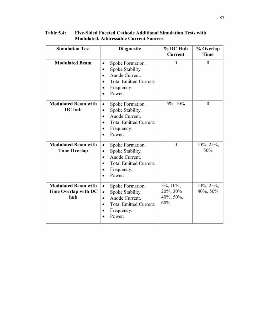
87
Table 5.4: Five-Sided Faceted Cathode Additional Simulation Tests with
Modulated, Addressable Current Sources.
Simulation Test Diagnostic % DC Hub
Current
% Overlap
Time
Modulated Beam Spoke Formation.
Spoke Stability.
Anode Current.
Total Emitted Current.
Frequency.
Power.
0 0
Modulated Beam with
DC hub Spoke Formation.
Spoke Stability.
Anode Current.
Total Emitted Current.
Frequency.
Power.
5%, 10% 0
Modulated Beam with
Time Overlap Spoke Formation.
Spoke Stability.
Anode Current.
Total Emitted Current.
Frequency.
Power.
0 10%, 25%,
50%
Modulated Beam with
Time Overlap with DC
hub
Spoke Formation.
Spoke Stability.
Anode Current.
Total Emitted Current.
Frequency.
Power.
5%, 10%,
20%, 30%
40%, 50%,
60%
10%, 25%,
40%, 50%

88
CHAPTER SIX: VORPAL SIMULATION RESULTS FOR THE CONTINUOUS
CURRENT SOURCE CATHODE MODEL
6.1 Overview
This chapter covers the simulation results of the continuous current source model
with the cylindrical and faceted cathodes in VORPAL. This model was tuned and tested
to develop a reference case for both geometries. The results obtained from both models
are compared with previous work [12] completed in ICEPIC.
6.2 Continuous Current Source Model: Cylindrical Cathode
The cylindrical cathode model was simulated in VORPAL; after tuning the
operating parameters, it was found that the most stable case for this configuration was at
a cathode-anode voltage ( caV ) of -26.0 kV, applied magnetic field ( B ) of 0.12 T, and a
continuous linear current density ( '
eJ ) of 500 A/m (total emitted current). These
parameters gave an operating frequency of 960 MHz. Figure 57-60 show the RF Bz field
for the rising sun magnetron with the cylindrical cathode, the mode switching during start
up, and the FFT of the cavity voltage, respectively from VORPAL. The plot of the RF Bz
field changes phase by 180° at adjacent cavities, indicating the π-mode operation.
Figure 59 shows a startup time of approximately 300 ns for oscillation. The linear
power density at the loaded cavity was calculated to be 3.9 MW/m for this configuration.
Figure 60 shows the results of this 2-D model (Vca=-26 kV, B=0.12 T, '
eJ =500 A/m)

89
presenting (a) the electron hub at 0.012 ns, before oscillation occurs and (b) the spokes
that have formed showing oscillation at a time of 276 ns. Figure 61 shows the total
emitted linear current density (B field is turned off in the simulation) to check the actual
injected current. Oscillatory behavior of the current is also observed in this plot. This can
be attributed to the numerical resolution in the PIC code. Since these macroparticles are
being collected on the anode, they are not emitted exactly the same for every time step;
therefore, this variation results in oscillations that will eventually average to the total
current injected. This diagnostic was designed for analysis, and its results should only be
used to determine the average value of the injected current. Figure 62 shows the anode
linear current density during the device normal operation, and the oscillation startup after
300 ns can be seen. The cylindrical cathode geometry was also simulated at Vca = -22.2
kV, B = 0.09 T, '
eJ = 326 A/m for comparison with the faceted cathode models. The
anode linear current density for this case can be observed in Figure 63.
An analysis of the startup current was also studied. The total emitted linear
current density was varied from 0.25J’e to 2J’e. Figure 64 shows a graph of startup time
versus the total emitter linear current density of the device for the cylindrical cathode and
other cathode geometries (five-sided and ten-sided cathode). This result illustrates the
variation in the startup time of the device for the different cathode geometries. From the
curve, it is observed that the magnetron starts at 310 ns for the cylindrical cathode at
Vca=-26 kV, B=0.12 T, '
eJ =500 A/m. Even though these parameters do not give the
fastest startup for this device, it does give the most stable model, showing clean spokes
and stable oscillations for the cylindrical cathode geometry. Note also that the startup
time levels off for J’e > 700 A/m but increases almost linearly below 700 A/m.

90
Figure 57: Cylindrical cathode model from VORPAL simulation showing the
RF B-field and π-mode. This result corresponds to Vca = -26.0 kV, B =
0.12 T, and J’e = 500 A/m.
Figure 58: Cylindrical cathode cavity voltage frequency versus time with moving
window, showing the startup time of the device at 300 ns, and the
mode switching from 650 MHz to the Operating Frequency (π-mode)
960 MHz from VORPAL.
Figure 59: Cylindrical cathode Fast Fourier Transform (FFT), over entire
simulation time, of the loaded cavity voltage from VORPAL
simulation. This plot clearly indicates that the π-mode is dominant at
the frequency of operation of 960 MHz.
Frequency (Hz)
FF
T A
mp
litu
de
Time (s)
Fre
qu
ency
(H
z)
Startup

91
(a) (b)
Figure 60: Cylindrical cathode VORPAL simulation results for Vc = -26.0 kV,
B = 0.12 T, and J’e = 500 A/m. The red dots indicate electron
macroparticles. Figure 61(a) is at 0.012 ns, before oscillation, and
Figure 61(b) is at 276 ns, after oscillation starts and the model is
stable.
Figure 61: Cylindrical cathode continuous total emitted linear current
density versus time with no applied magnetic field (B=0).
Figure 62: Cylindrical cathode continuous anode linear current density
during device operation versus time.
Time (s) C
urr
ent
Den
sity
(A
/m)
Time (s) C
urr
ent
Den
sity
(A
/m)
7

92
Figure 63: Cylindrical cathode (Vca = -22.2 kV, B = 0.09 T, '
eJ = 326 A/m)
continuous anode linear current density during device operation
versus time.
Figure 64: Startup time versus continuous total emitted linear current
density for different cathode geometries: cylindrical and
faceted.
6.3 Continuous Current Source Model: Five-Sided Faceted Cathode
A five-sided faceted cathode with a vertex angle of 3π/2 was then simulated as a
replacement for the cylindrical cathode with all other parameters in the calculation
unchanged. It was found that the reference parameters: caV = -26.0 kV, B = 0.12 T, and a
'
eJ = 500 A/m were not the optimum for this configuration. The spokes were unstable and
Time (s) C
urr
ent
Den
sity
(A
/m)

93
a clean oscillation was not observed. Using the results from a previous model [12]
developed in ICEPIC, these parameters were changed to caV = -22.2 kV, B = 0.09 T, and
a '
eJ = 326 A/m. It was found that the model developed in ICEPIC and the VORPAL
models were comparable. With these parameters the five-sided faceted cathode was able
to oscillate at a frequency of 957 MHz. The cylindrical cathode model was also simulated
using these same parameters for comparison purposes. Figure 65 shows the RF Bz field,
indicating the π-mode operation for the five-sided faceted cathode. Figure 66 shows the
mode switching during start up. Initially there is a 650 MHz mode before stable
operation. Figure 67 shows the FFT of the cavity voltage, with a clear peak at 957 MHz.
The linear power density at the loaded cavity was calculated to be 1.2 MW/m.
Figure 65: Five-sided faceted cathode model from VORPAL simulation
showing the RF B-field and π-mode. This result corresponds to
Vca = -22.2 kV, B = 0.09 T, and J’e = 326 A/m.

94
Figure 66: Five-sided faceted cathode cavity voltage frequency versus time with
moving window, showing the startup time of the device at 200 ns, and
the mode switching from 650 MHz to the operating frequency (π-
mode) 957 MHz from VORPAL.
Figure 67: Five-sided faceted cathode Fast Fourier Transform (FFT), over entire
simulation time, of the loaded cavity voltage from VORPAL
simulation. This plot indicates that the π-mode is dominant at the
frequency of operation of 957 MHz.
The spoke formation results are shown in Figure 68. Figure 68(a) shows the pre-
oscillation state (t= 0.012 ns). Figure 68(b) shows the spokes forming after oscillation at
t= 317 ns. These VORPAL results, both cylindrical and faceted cathodes, were compared
with a 2-D simulation previously performed in ICEPIC [12]. It was found that the
cylindrical cathode at caV = -26.0 kV, B = 0.12 T, and a '
eJ = 500 A/m modeled in
VORPAL was a more stable simulation with very clean spokes compared to the
simulation parameters used in ICEPIC (-22.2 kV, 0.09 T, 326 A/m). However, the
Time (s)
Fre
qu
ency
(H
z)
Startup
Frequency (Hz)
FF
T A
mp
litu
de
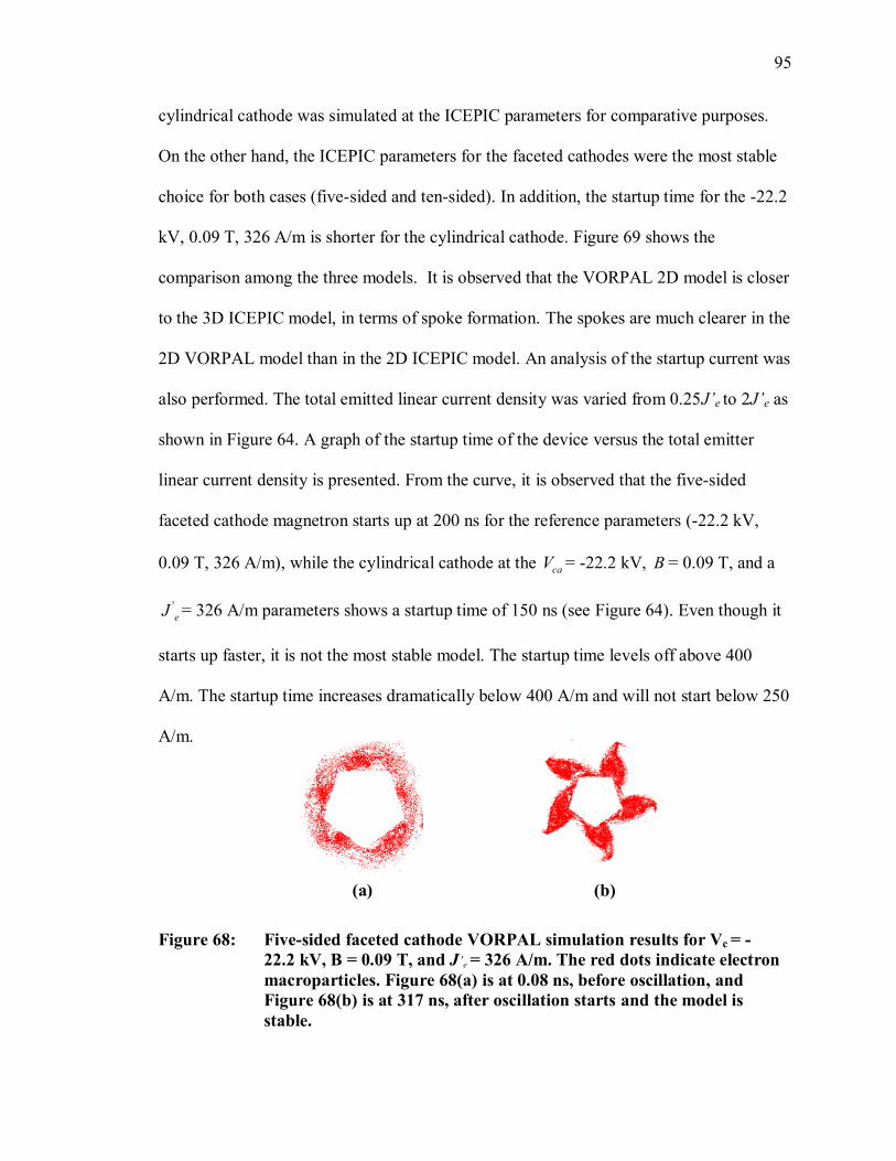
95
cylindrical cathode was simulated at the ICEPIC parameters for comparative purposes.
On the other hand, the ICEPIC parameters for the faceted cathodes were the most stable
choice for both cases (five-sided and ten-sided). In addition, the startup time for the -22.2
kV, 0.09 T, 326 A/m is shorter for the cylindrical cathode. Figure 69 shows the
comparison among the three models. It is observed that the VORPAL 2D model is closer
to the 3D ICEPIC model, in terms of spoke formation. The spokes are much clearer in the
2D VORPAL model than in the 2D ICEPIC model. An analysis of the startup current was
also performed. The total emitted linear current density was varied from 0.25J’e to 2J’e as
shown in Figure 64. A graph of the startup time of the device versus the total emitter
linear current density is presented. From the curve, it is observed that the five-sided
faceted cathode magnetron starts up at 200 ns for the reference parameters (-22.2 kV,
0.09 T, 326 A/m), while the cylindrical cathode at the caV = -22.2 kV, B = 0.09 T, and a
'
eJ = 326 A/m parameters shows a startup time of 150 ns (see Figure 64). Even though it
starts up faster, it is not the most stable model. The startup time levels off above 400
A/m. The startup time increases dramatically below 400 A/m and will not start below 250
A/m.
(a) (b)
Figure 68: Five-sided faceted cathode VORPAL simulation results for Vc = -
22.2 kV, B = 0.09 T, and J’e = 326 A/m. The red dots indicate electron
macroparticles. Figure 68(a) is at 0.08 ns, before oscillation, and
Figure 68(b) is at 317 ns, after oscillation starts and the model is
stable.

96
Figure 69: Comparison of ICEPIC model versus VORPAL model. Vca = -22.2 kV,
B = 0.09 T, and J’e = 326 A/m. The top figures show the cylindrical
cathode model, the middle figures show the five-sided faceted cathode,
and the bottom figures show the ten-sided faceted cathode.
Figure 70 shows the total emitted linear current density versus time for the five-
sided faceted cathode. These results were taken with no applied B field, so all the emitted
current will be collected at the anode. This was completed to check that the total current
3D ICEPIC 2D ICEPIC 2D VORPAL

97
injected to the device was correct. In the figure, it is observed that the current averages to
approximately 326 A/m, which matches the current input in the model.
Figure 71 shows the anode linear current density versus time when the device is in
operation. It was found that there is an instability in the five-sided cathode oscillations.
As it can be observed in Figure 71, this instability results in a current spike to the anode
and a subsequent collapse of the spokes. Figure 72 shows the transition of the spokes
before the current spike occurs, at the current spike, and after the current spike, when the
spokes collapse. For this particular example, the time between 119.8 ns and 143.5 ns was
selected. It can be observed that the shape of the spokes changes at the current spike with
the electrons forming a more concentrated cloud or clump; then, the clump extends to the
anode when the spike occurs. The result is a loss of a large percentage of available
electrons. Then, the spokes disconnect and collapse. Following this mechanism, the
spokes will form again. As can be seen in Figure 71, this current spike has a periodic
behavior. The spike occurs, approximately every 250 ns to 350 ns. This means that every
time the current spike occurs the spokes will collapse and reform again. Since the
geometry of the cathode consists of five sides, the time that it takes the spokes to go
around the cathode is 5τRF, where 1 τRF = 1.04 ns corresponds to one facet. Therefore, the
periodicity of the instability could be related to a multiple of the RF period. The causes of
this instability are mainly attributed to the cathode shape, but further studies are needed
to completely understand it. The electron trajectories around the five-sided cathode
become distorted and appear to create too many synchronous electrons. These electron
clumps give up their energy almost simultaneously, resulting in the current spike. By
implementing a ten-sided cathode geometry (increasing the number of facets), this

98
problem was reduced. Therefore, the remainder of the phase control research work used
the ten-sided cathode geometry.
Figure 70: Five-sided faceted cathode continuous total emitted linear
current density versus time with no applied magnetic field (B=0) .
Figure 71: Five-sided faceted cathode continuous anode linear current
density during device operation versus time. The periodic current
spikes are followed by spoke collapse.
(a) (b) (c)
Figure 72: Five-sided faceted cathode showing the transition of the spokes
during the current instability. Spokes are shown (a) before current
spike at 119.8 ns, (b) at current spike at 121.32 ns, and (c) after
spokes collapse at 143.5 ns.
Time (s) C
urr
ent
Den
sity
(A
/m)
Time (s) C
urr
ent
Den
sity
(A
/m)
-6

99
6.4 Continuous Current Source Model: Ten-Sided Faceted Cathode
The ten-sided faceted cathode geometry was chosen to minimize the current spike
problem. Similar analysis was completed for this configuration. The model was simulated
at the same reference parameters: Vca = -22.2 kV, B = 0.09 T, and J’e = 326 A/m. Figure
73 shows the RF Bz field and illustrates the π-mode for the ten-sided faceted cathode.
Figure 74 shows the start up time for this device at approximately 110 ns; Figure 75
shows the FFT of the cavity voltage. The plot in Figure 75 indicates the π-mode operation
at a frequency of 957 MHz; the 650 MHz peak is still present in this configuration. The
linear power density at the loaded cavity was calculated to be 1.2 MW/m, which was the
same as for the five-sided cathode.
Figure 73: Ten-sided faceted cathode model from VORPAL simulation
showing the RF B-field and π-mode. This result corresponds to Vca = -
22.2 kV, B = 0.09 T, and J’e = 326 A/m.

100
Figure 74: Ten-sided faceted cathode cavity voltage frequency versus time with
moving window, showing the startup time of the device at 110 ns,
showing the operating frequency (π-mode) at 957 MHz from
VORPAL.
Figure 75: Ten-sided faceted cathode Fast Fourier Transform (FFT), over entire
simulation time, of the loaded cavity voltage from VORPAL
simulation. This plot indicates that the π-mode is dominant at the
frequency of operation of 957 MHz.
Figure 76 shows the total emitter linear current density for the ten-sided faceted
cathode. This simulation was performed with no applied B field. From the figure, it can
be seen that the total emitted current averages to approximately 326 A/m, which matches
the input current. Figure 77 shows the anode linear current density when the device is in
operation. These results indicate a behavior very similar to the anode current for the
cylindrical cathode geometry (see Figure 62), but the large current spikes are not present
as in the five-sided cathode model. Instead there is a large spike at ≈ 110 ns, and then the
oscillations are more stable. This result indicates that the ten-sided cathode geometry
reduced the current instability.
Time (s)
Fre
qu
ency
(H
z)
Startup
Frequency (Hz)
FF
T A
mp
litu
de
2.0x10⁹

101
Figure 76: Ten-sided faceted cathode continuous total emitted linear
current density versus time with no applied magnetic field (B=0).
Figure 77: Ten-Sided faceted cathode continuous anode linear current
density during device operation versus time.
The simulation for this case was also run for various emitted current densities, and
the startup times were determined from the frequency versus time plots in VORPAL.
Figure 64 shows the graph of startup time versus total emitted linear current density for
various cathode geometries. From this graph, it can be seen that the ten-sided cathode
geometry has a startup of 110 ns for the reference parameters. As can be seen, the startup
time increases for lower current densities and decreases for higher current densities as
expected. From this plot, the three cases: cylindrical, five-sided cathode, and ten-sided
show very similar startup times for the reference parameters; however, as the linear
current density is decreased (below 326 A/m), the startup times are not so similar
depending on cathode shape. It is also noticeable that the cylindrical cathode for the Vca =
Time (s) C
urr
ent
Den
sity
(A
/m)
Time (s) C
urr
ent
Den
sity
(A
/m)

102
-22.2 kV, B = 0.09 T, and J’e = 326 A/m parameters does not start for current density
values below 230 A/m. It was found that for this geometry, there is an increase in mode
competition between the 650 MHz mode and the 957 MHz (π-mode); therefore, for
values below 230 A/m, the device switches to the lower mode and does not start in π-
mode. The nature of this behavior for this particular case needs further study and
analysis.
The next step in the simulations is the study of the modulated, addressable,
current sources at the operating frequency. This aspect of the work will be discussed in
Chapter 7.
6.5 Summary of Results
This chapter studied the continuous current source model for the cylindrical and
faceted cathodes. From the results, it is observed that all three models operated at the π-
mode with frequencies of 960 MHz and 957MHz, respectively. A current instability was
found in the five-sided faceted cathode. This current instability resulted in current spikes,
which led to spokes disconnecting and collapsing. The ten-sided faceted cathode reduced
this current instability and improved the overall startup time of the device from 200 ns
(five-sided cathode) to 110 ns for the reference parameters; however, as the linear current
density is decreased (below 326 A/m), the startup times are not so similar depending on
cathode shape. Overall, the ten-sided cathode improved stability of the magnetron.

103
CHAPTER SEVEN: VORPAL SIMULATION RESULTS FOR THE MODULATED,
ADDRESSABLE CATHODE
7.1 Overview
This chapter describes the results for the modulated, addressable cathode current
source model. Two geometries were studied using this concept: a five-sided faceted
cathode and a ten-sided faceted cathode. Work was completed for both cathodes;
however, most of the analysis was performed on the ten-sided. Results showing the
modulation technique and phase control will be presented in this chapter.
7.2 Modulated Five-Sided Faceted Cathode
Modulated, addressable, discrete current sources were modeled from each facet of
the five-sided cathode to study its effect on the magnetron operation. Each facet on the
five-sided cathode structure contains 5 emitters that can be addressed spatially and
modulated temporally. The discrete current sources allow control in space and time of the
current injection. Each ON emitter mimics the location of the electron spoke. The number
of emitters can be varied; 5 emitters per side were chosen because it provided a
reasonable spoke width; since this technique results in the injection of the electrons all in
phase, the width of the spoke is important to allow the device to start. This modulation
technique allows control of the startup and location of the spokes. For this simulation, the
step size was modified to an integer fraction of the RF period. So for the 957 MHz
operating frequency, the time step is set to a multiple of τRF /N, where τRF =1.04 ns is an

104
RF period and N is the number of emitters, which is 5 emitters for this case. Therefore,
τRF /N = 0.208 ns, and the step size was chosen to be 1.0 ps. Figure 78 shows an example
of the setup for the discrete current sources, when they are all ON at the same time.
Figure 79 shows a diagram of the modulated current sources at the frequency of
operation. For demonstration purposes, the B field was turned OFF to show the emitters
turning ON in sequence. The diagrams show one RF period. The frequency of
modulation is 957 MHz, τrf = 1.04 ns, and Δt =1/5τRF.
(a) (b)
Figure 78: Five-sided faceted cathode showing discrete current sources setup
for (a) 0.0987 ns and (b) 0.197 ns. There are five emitters per facet. All
emitters are ON at the same time.
Emitters
Cathode
Anode
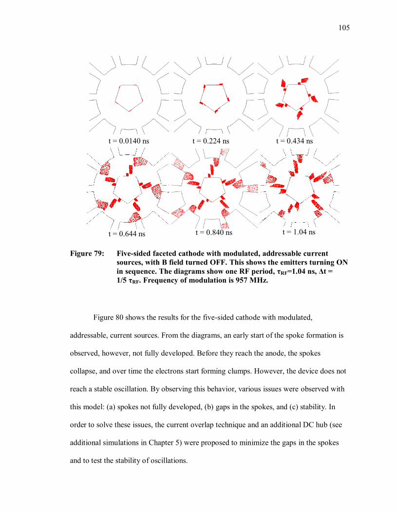
105
Figure 79: Five-sided faceted cathode with modulated, addressable current
sources, with B field turned OFF. This shows the emitters turning ON
in sequence. The diagrams show one RF period, τRF=1.04 ns, Δt =
1/5 τRF. Frequency of modulation is 957 MHz.
Figure 80 shows the results for the five-sided cathode with modulated,
addressable, current sources. From the diagrams, an early start of the spoke formation is
observed, however, not fully developed. Before they reach the anode, the spokes
collapse, and over time the electrons start forming clumps. However, the device does not
reach a stable oscillation. By observing this behavior, various issues were observed with
this model: (a) spokes not fully developed, (b) gaps in the spokes, and (c) stability. In
order to solve these issues, the current overlap technique and an additional DC hub (see
additional simulations in Chapter 5) were proposed to minimize the gaps in the spokes
and to test the stability of oscillations.
t = 0.0140 ns t = 0.224 ns t = 0.434 ns
t = 0.644 ns t = 0.840 ns t = 1.04 ns

106
7.3 Modulated Five-Sided Faceted Cathode with Time Overlap
The time overlap technique discussed in Chapter 5 was implemented in this
model. Different percentages of time overlap were tested; only the best and most stable
results are shown in Figure 81. The diagrams in Figure 81 show the case with a current
overlap of 25%. The frequency of modulation is 957 MHz, τRF = 1.04 ns, Δt = 1/5 τRF,
where the overlap time corresponds to τov = 0.0520 ns. It is observed in the figure that the
overlap technique did fix part of the problem; parts of the gaps are covered, and the
spokes are clearly formed going from the transition of electron clumps to fully developed
spokes. However, the model was still not very stable, and as further study was completed,
the same current instability present in the five-sided faceted cathode with a continuous
current source was also found with the modulated plus current overlap model approach.
Figure 82 shows the modulated total emitted linear current density. This
simulation was completed with no applied B field to check the input current. The current
density averages to approximately 326 A/m as expected. Figure 83 shows the anode
linear current density during the device operation, and as was mentioned before, the
instability is also present in this case at t ≈ 100 ns. Since this simulation was run for a
shorter time, the current spike can be seen in more detail. The spokes were inspected for
corresponding times that match the transition before and after the current spike as shown
in Figure 84. Figure 85 shows the corresponding Fast Fourier Transform (FFT) of the
cavity voltage, which indicates the device is operating at a frequency of 957 MHz. This
plot also shows the lower frequency mode of 650 MHz is still present. Also, it can be
seen in the figure that the FFT peak is wider compared to the other model cases
(cylindrical and faceted with continuous current source); the cause of this spread is
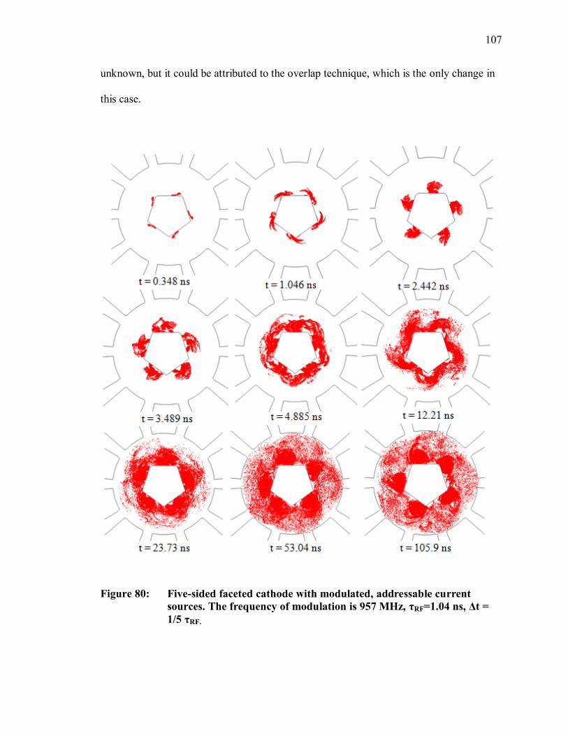
107
unknown, but it could be attributed to the overlap technique, which is the only change in
this case.
Figure 80: Five-sided faceted cathode with modulated, addressable current
sources. The frequency of modulation is 957 MHz, τRF=1.04 ns, Δt =
1/5 τRF.

108
Figure 81: Five-sided faceted cathode with modulated, addressable current
sources plus current overlap. This diagram shows the case for current
overlap of 25%. The frequency of modulation is 957 MHz, τRF = 1.04
ns, Δt = 1/5 τRF, τov = 0.0520 ns.
t = 0.399 ns t = 1.198 ns t = 2.397 ns
t = 3.596 ns t = 4.795 ns t = 12.38 ns
t = 23.57 ns t = 53.15 ns t = 105.1 ns
t = 108.7 ns t = 109.8 ns t = 111.8 ns

109
Figure 82: Modulated total emitted linear current density versus time with
no applied magnetic field (B=0) for five-sided faceted cathode
with 25% overlap.
Figure 83: Modulated anode linear current density versus time during
device operation for the five-sided faceted cathode with 25% overlap,
showing current spike at around 102 ns.
Figure 84: Transition of the spokes during the current instability for the
modulated, addressable current sources for the five-sided faceted
cathode with 25% overlap. Spokes are shown (a) before current
spike at 110.3 ns, (b) at current spike at 113.1 ns, and (c) after
spokes collapse at 116.3 ns.
Time (s) C
urr
ent
Den
sity
(A
/m)
Time (s) C
urr
ent
Den
sity
(A
/m)
8

110
Figure 85: Fast Fourier Transform (FFT) of the loaded cavity voltage from
VORPAL Simulation for the modulated, addressable, current
source for the five-sided faceted cathode with 25% overlap. This plot
indicates that the π-mode is dominant at the frequency of operation of
957 MHz.
Furthermore, it is noticed that for this model with current overlap, the current
spike is more pronounced in terms of the spoke shape (thin and long spokes extending
inside the anode cavity). The clumps extend towards the anode as the anode current goes
very high and then collapse as they try to recover. This effect could be attributed to the
modulation technique, because the electrons are controlled and injected synchronous with
the RF field, a large fraction of the electrons travel to the anode, and there are not enough
asynchronous electrons that go back to the cathode and keep the process going.
7.4 Modulated Five-Sided Cathode with Time Overlap and DC Hub
The DC hub technique was combined with the overlap to fill the gaps and feed
electrons to the spokes to maintain stability. Different percentages of current were
simulated for the DC hub. Figure 86 shows the best result with a 5% J’e DC hub. The DC
hub is shown with the green electron macroparticles, and the overlap electrons are shown
in red. In VORPAL, this is an interchangeable feature; the green electrons were chosen to
be on top of the red to demonstrate that the spoke gaps and voids were filled by the
Frequency (Hz)
FF
T A
mp
litu
de

111
implementation of the DC hub. In Figure 87, an example of the model with modulated
overlap case is shown next to the model with only the DC hub electrons shown. Here the
different electrons sources can be distinguished. The DC hub was a good solution to the
stability and gap problem, as can be seen in Figure 86. The device starts oscillating; the
spokes look very well formed, and stability of the model is improved. However, the
issues presented with the five-sided, faceted cathode require more study and simulation to
develop stable oscillations and to improve startup time. Even though this additional
analysis was considered, it was found that a simpler solution to minimize the problems
was to use the ten-sided faceted cathode. This model is covered in the next section.
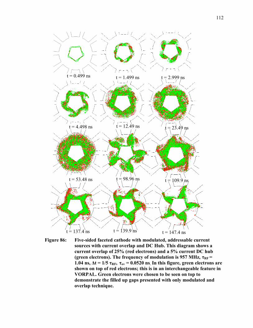
112
Figure 86: Five-sided faceted cathode with modulated, addressable current
sources with current overlap and DC Hub. This diagram shows a
current overlap of 25% (red electrons) and a 5% current DC hub
(green electrons). The frequency of modulation is 957 MHz, τRF =
1.04 ns, Δt = 1/5 τRF, τov = 0.0520 ns. In this figure, green electrons are
shown on top of red electrons; this is in an interchangeable feature in
VORPAL. Green electrons were chosen to be seen on top to
demonstrate the filled up gaps presented with only modulated and
overlap technique.
t = 0.499 ns t = 1.499 ns t = 2.999 ns
t = 4.498 ns t = 12.49 ns t = 23.49 ns
t = 53.48 ns t = 98.96 ns t = 109.9 ns
t = 137.4 ns t = 139.9 ns t = 147.4 ns

113
Figure 87: Five-sided faceted cathode showing: on the left column the modulated
plus current overlap (25% overlap) simulation electrons and on the
right the DC hub (5% J’e) electrons. It shows the comparison between
the two, and it can be seen that the gaps are filled by the green DC
hub electrons.
t = 137.4 ns
t = 139.9 ns
t = 147.4 ns

114
7.5 Modulated Ten-Sided Faceted Cathode
The ten-sided, faceted cathode was chosen to reduce the stability issues presented
with the five-sided faceted cathode. It was found that this geometry gave a more stable
model; therefore, it was used for the remaining studies. The ten-sided cathode contains 3
emitters per facet, which can be turned ON and OFF at any desired time. Since for the
rising sun magnetron the π-mode is the primary mode, the 10-cavity device has 5 spokes
in π-mode. Therefore, a single spoke rotates past 2 cathode facet plates (6 emitters total)
every RF period. For this reason, 5 total emitters were turned ON simultaneously on
every other facet at the same facet location at a frequency of 957 MHz with an ON time
of 1/6τRF. Figure 88 shows the setup of the discrete current sources on the ten-sided
faceted cathode, showing 3 emitters per facet with all of the emitters ON at the same time
for demonstration purposes.
(a) (b)
Figure 88: Ten-Sided Faceted cathode showing discrete current sources setup
for (a) 0.0163 ns and (b) 0.326 ns. There are three emitters per facet.
All emitters are ON at the same time.

115
Figure 89 shows the diagrams with no applied B field to show the emitters turning
ON in sequence. This example shows one RF period of the simulation. It can be seen that
5 emitters are initially turned ON at the same time on every other facet, and then these are
followed by the remaining emitters as they complete the first RF period of the simulation.
Figure 89: Ten-sided faceted cathode with modulated, addressable current
sources, with B field turned OFF. This shows the emitters turning ON
in sequence. The diagrams show one RF period (two facets),
τRF=1.04ns, Δt = 1/6 τRF. Frequency of modulation is 957 MHz.
t = 0.0943 ns t = 0.179 ns t = 0.353 ns
t = 0.528 ns t = 0.707 ns t = 0.877 ns
t = 1.04 ns
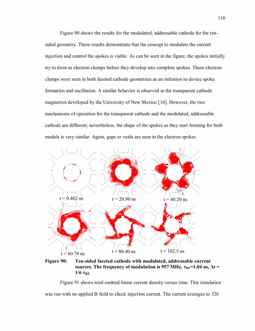
116
Figure 90 shows the results for the modulated, addressable cathode for the ten-
sided geometry. These results demonstrate that the concept to modulate the current
injection and control the spokes is viable. As can be seen in the figure, the spokes initially
try to form as electron clumps before they develop into complete spokes. These electron
clumps were seen in both faceted cathode geometries as an initiation to device spoke
formation and oscillation. A similar behavior is observed in the transparent cathode
magnetron developed by the University of New Mexico [16]. However, the two
mechanisms of operation for the transparent cathode and the modulated, addressable
cathode are different; nevertheless, the shape of the spokes as they start forming for both
models is very similar. Again, gaps or voids are seen in the electron spokes.
Figure 90: Ten-sided faceted cathode with modulated, addressable current
sources. The frequency of modulation is 957 MHz, τRF=1.04 ns, Δt =
1/6 τRF.
Figure 91 shows total emitted linear current density versus time. This simulation
was run with no applied B field to check injection current. The current averages to 326
t = 0.402 ns t = 20.90 ns t = 40.20 ns
t = 60.70 ns t = 80.40 ns t = 102.5 ns
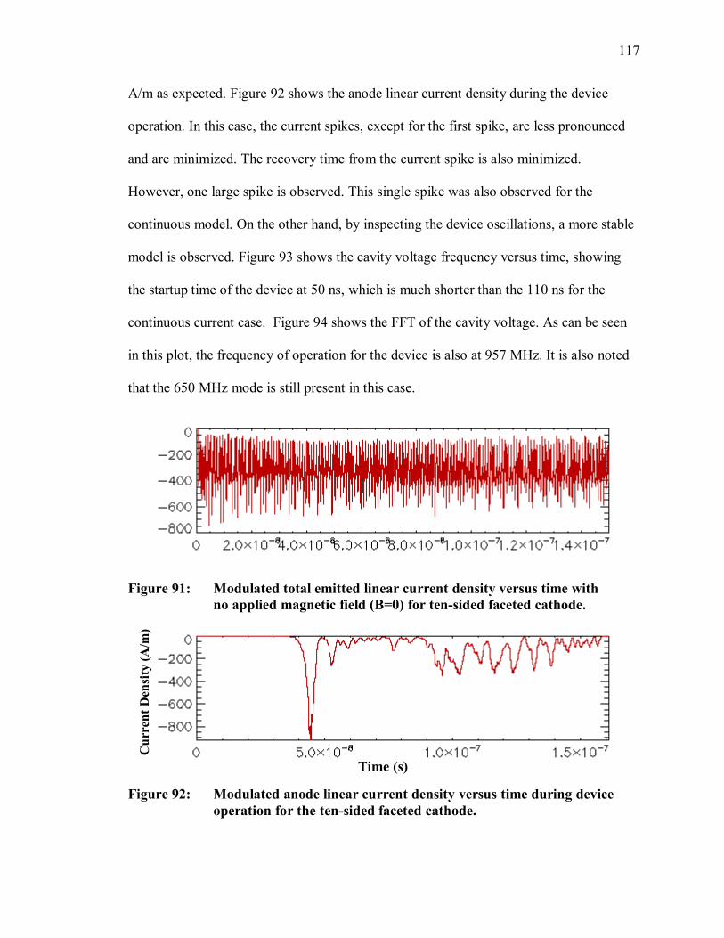
117
A/m as expected. Figure 92 shows the anode linear current density during the device
operation. In this case, the current spikes, except for the first spike, are less pronounced
and are minimized. The recovery time from the current spike is also minimized.
However, one large spike is observed. This single spike was also observed for the
continuous model. On the other hand, by inspecting the device oscillations, a more stable
model is observed. Figure 93 shows the cavity voltage frequency versus time, showing
the startup time of the device at 50 ns, which is much shorter than the 110 ns for the
continuous current case. Figure 94 shows the FFT of the cavity voltage. As can be seen
in this plot, the frequency of operation for the device is also at 957 MHz. It is also noted
that the 650 MHz mode is still present in this case.
Figure 91: Modulated total emitted linear current density versus time with
no applied magnetic field (B=0) for ten-sided faceted cathode.
Figure 92: Modulated anode linear current density versus time during device
operation for the ten-sided faceted cathode.
Time (s) C
urr
ent
Den
sity
(A
/m)

118
Figure 93: Modulated ten-sided faceted cathode cavity voltage frequency versus
time with moving window, showing the startup time of the device at
50 ns showing the operating frequency (π-mode) at 957 MHz from
VORPAL.
Figure 94: Fast Fourier Transform (FFT), over entire simulation time, of the
loaded cavity voltage from VORPAL simulation for the modulated,
addressable, current source, ten-sided faceted cathode. This plot
indicates that the π-mode is dominant at the frequency of operation of
957 MHz.
7.6 Modulated Ten-Sided Faceted Cathode with DC Hub
For the ten-sided cathode geometry, it was not necessary to implement the current
overlap technique because the model showed oscillations just with the modulation of the
current only. However, as can be seen in Figure 90, some holes and gaps were observed
in the spokes; to fix this problem, a 5% J’e DC hub was implemented to cover the gaps.
This result is shown in Figure 95. The green electrons show the DC hub, and the red
electrons are the particles corresponding to the modulated only case. It is observed that
Startup time, ~ 50 ns
Startup
Cavity Voltage FFT vs. time with
moving window
Frequency (Hz)
FF
T A
mp
litu
de
Startup

119
the DC hub successfully fills up the holes in the spokes. Therefore, the DC hub could be
used to minimize problems with the spoke formation in the modulated case.
Figure 95: Ten-sided faceted cathode with modulated, addressable current
sources with DC Hub. This diagram shows a 5% current DC hub
(green electrons). The frequency of modulation is 957 MHz, τRF = 1.04
ns, Δt = 1/6 τRF.
The startup time was also studied for this particular geometry; it was found that
the ten-sided modulated case has a shorter startup time than all other cases with
oscillations starting as soon as 35 ns (see Figure 96). The modulation reduces startup time
as was expected. In general, the modulated case cuts the startup time by greater than
50%. As the current density is decreased, the startup time increases, but more slowly than
for the continuous current cases. Similarly to the cylindrical cathode model, the
t = 0.402 ns t = 20.10 ns t = 40.20 ns
t = 60.70 ns t = 101.3 ns t = 118.2 ns

120
modulated ten-sided faceted cathode does not start for currents below 230 A/m. For
currents < 230 A/m, the device switches completely to the lower mode 650 MHz
frequency, and it never starts at the π-mode. As mentioned previously, the cause of this
behavior needs further study.
Figure 96: Comparison of startup time versus total emitted linear current
density for different cathode geometries: cylindrical and faceted,
including continuous current source model and the modulated,
addressable current source model for the ten-sided faceted
cathode.
Figure 97 shows a plot of the anode current density, J’a, versus the total emitted
linear current density, J’e, for the ten-sided faceted cathode with continuous current
source and with the modulated current source. As can be observed in the curves, the
anode current density drawn by the device increases roughly linearly with the total
emitted linear current density. It is also observed that the modulated, addressable cathode
draws more current than the continuous source model, which means there is an increase
in the linear input power density. This result was expected from the modulated,

121
addressable cathode because electrons are injected in phase. Hence, they will be
synchronous and will be more likely to give up energy and transit to the anode.
Table 7.1 shows a summary of results of the linear anode current density, the
calculated input power density, the loaded cavity power, and the calculated efficiency for
the different cathode geometries at the reference parameters Vca = -22.2 kV, B = 0.09 T,
and J’e = 326 A/m. It is observed that the loaded cavity power is very similar for the three
cathode geometries with a continuous current source. The loaded cavity power results
also show that the modulation technique increases the output power density and
efficiency, as was expected, showing an efficiency of about 95.4%. For the modulated
case, the anode current density increases to 100 A/m, and the output power
approximately doubles to 2.1 MW/m. Overall, the efficiency increases from 80-85% to
95%. Note, this efficiency should not be taken as absolute value and should only be used
for comparison with the continuous current source cases. As was mentioned in Chapter 5,
this is a 2D simulation, and there is no real output port; therefore, this power density is
not the real coupled output power. However, these results can be used as a relative
estimation of the power at the loaded cavity as a demonstration of the modulated cathode
increasing the loaded cavity power as was expected.
Figure 98 shows a graph of the loaded cavity power density versus the total
emitted linear current density. It is observed that the loaded cavity power density curves
present an almost linear increase in power as the emitted current density increases. This
behavior is also comparable to the same linear increase in anode current as the total
emitted current density increases in the previous figure. As can be seen in the figure, the
power density goes up as the emitted current increases; it is clear from the curve that the

122
modulated current model has a higher loaded cavity power density than the continuous
current source model.
Table 7.1: Current densities, power densities, and efficiencies for various
cathode geometries: cylindrical, five-sided and ten-sided cathode for
the reference parameters Vca = -22.2 kV, B = 0.09 T, and J’e = 326
A/m.
Cathode Anode
Current
Density J’a
(A/m)
Input Power
Density
(MW/m)
Loaded Cavity
Power Density
(MW/m)
Efficiency η
(%)
Continuous
Current Cylindrical
60.81 1.35 1.0 74.3
Continuous
Current Five-Sided
69.36 1.54 1.2 77.9
Continuous
Current Ten-Sided
67.56 1.5 1.2 80.0
Modulated Current
Ten-Sided
100 2.2 2.1 95.4
Figure 97: Anode current density versus total emitted linear current density for
the ten-sided faceted cathode with continuous current source and
modulated current source.

123
Figure 99 shows the plot of efficiency versus injected current density for both the
continuous current source and the modulated current source model for the ten-sided
faceted cathode. The modulated current curve shows higher efficiencies until J’e ≈ 500
A/m. It is observed that the maximum efficiency is obtained at the reference parameters
Vca = -22.2 kV, B = 0.09 T, and J’e = 326 A/m in both models. As the current increases,
the efficiency decreases, and the efficiency curves for the two cases (continuous and
modulated current source) start to merge. At this point, for high current densities (J’e >
500 A/m), the space charge effects become more significant, and the hub will get closer
to the anode. This will result in the electrons having less potential energy to give up, and
therefore, the loaded cavity power absorbed will be less. Even though the spokes are
formed, they will start to spread out because of the space charge effects; therefore, the
peak fields will saturate. This saturation will limit the device efficiency. Therefore, the
advantages of using a modulated current source are no longer applicable for this regime.
Figure 98: Loaded cavity power versus total emitted linear current density for
the ten-sided faceted cathode with continuous current source and
modulated current source.

124
Figure 99: Efficiency versus total emitted linear current density for the ten-sided
faceted cathode with continuous current source and modulated
current source.
7.7 Modulated Ten-Sided Faceted Cathode with Active Phase Control
After these studies, the simulation of the ten-sided cathode was run three different
times for both the modulated and the reference (non-modulated) cases. Figure 100 shows
the spokes during oscillation. For the modulated case (Figure 100(a)), the spokes are at
the same exact location at the same simulation time (76.38 ns); it can be seen that the
spokes remain at the same location because of the modulated current control. Note that
while the two bottom spoke simulations are very similar, they are not identical. For the
reference case (Figure 100(b)), it shows that the spokes are at three different locations at
the same simulation time (322.12 ns) because of the random startup nature of the
magnetron. Hence, the modulated, addressable cathode controls the magnetron startup
and RF phase.

125
(a) (b)
Figure 100: Ten-sided faceted cathode with (a) Modulated, addressable current
sources: Spokes are aligned at the same location in time (76.38 ns) for
three different simulation runs, (b) Continuous current source:
Spokes are not aligned at the same location in time (322.12 ns) for
three different simulation runs.
Using the modulated, addressable, cathode, the phase can also be dynamically
controlled. The next results show the case when a phase shift of 180° is driven during
oscillation. The phase shift is initiated at 88.4 ns during a reference simulation run, after
the device has achieved stable oscillation. As can be seen in Figure 101, the spokes are
shown at a time of 82 ns before the 180° shift. Then 14 RF periods later, at a time of 96.8
ns when the spokes have shifted 88.5°, the spokes are shown again in Figure 101(b). The
spokes are then shown at two additional times after the phase shift (17τRF, 35τRF). The

126
spokes clearly shift location over these times. As can be seen in Figure 101 (d), the
spokes have fully shifted location to the adjacent cavities after 35 RF periods,
demonstrating the 180° shift as expected. However, these results demonstrate that the
modulated, addressable cathode can be used to actively control the RF phase.
Figure 101: Ten-sided faceted cathode with modulated addressable current
sources, showing transition to a phase shift of 180°. (a) Reference
case: Phase = 0° at 82.0 ns, phase shift initiated at 88.40 ns, (b) after
14.5 RF periods (t = 96.8 ns) from the reference, 8 RF periods from
the phase shift, (c) after 17 RF periods (t = 100.0 ns), 11 RF periods
from the phase shift, (d) after 35 RF periods (t = 118.4 ns), 29 RF
periods from the phase shift.

127
Figure 102 shows the RF Bz field versus reference time for the ten-sided case with
modulated, addressable, current sources. These plots show the transition of the phase
shift initiated at 88.40 ns. The RF Bz curves show the shift 14, 17, and 35 RF periods
after the reference point. Note that the x-axis is a referenced time with the purpose of
showing the phase shift. The real time windows were chosen to cover these ranges: the
phase 0° reference at t = 82 ns, phase = 88.5° at t = 96.8 ns, phase = 160.05° at 100 ns,
and phase = 178.9° at t = 118.4 ns. These RF Bz curves (Figure 102) also corroborate the
results obtained by visually inspecting the spoke phase shift in Figure 101. Figure 103
shows the cavity voltage frequency versus time with the phase shift. In this plot, it can be
observed that after the phase is shifted, the model is stable, and the π-mode operation at
957 MHz is maintained.

128
(a)
(b)
(c)
Figure 102: RF Bz field vs. reference time; showing transition to a phase shift of
180° initiated at 88.40ns. Reference: Phase=0° (a) After 14.5 RF
periods (t=96.8ns) from reference, 8 RF periods from phase shift, (b)
after 17 RF Periods (t=100.0ns) from reference, 11 RF periods from
phase shift, (c) after 35 RF Periods (t=118.4ns) from reference, 29 RF
periods from phase shift.

129
Figure 103: Modulated ten-sided faceted cathode cavity voltage frequency versus
time, showing the startup time of the device with phase shift initiated
at 88.40 ns. The operating frequency (π-mode) is at 957 MHz from
VORPAL.
Finally, in Figure 104, a curve of the phase versus time is graphed. The phase is
determined from the RF Bz plots referenced to the phase = 0° case. The graph shows the
transition from 0° to 180°. As can be seen in the curve, the phase change occurs slowly
until it completely transitions to steady state at 180°. This temporal transition is due to
the quality factor, Q, of this magnetron. For higher quality factors, typical for oscillators,
it is difficult to have instant changes in phase, as was expected. It can be seen in the
results that it takes approximately 25 RF periods after the phase change for the device to
fully shift phase to 180°. Therefore, for future work, the study of the phase shift with
different values of Q should be considered. It is expected that for a lower quality factor
the phase shift (transition from phase 0° to desired phase) will occur more rapidly.
Phase shift initiated

130
Figure 104: Phase versus RF Periods. Curve for the ten-sided faceted cathode
with modulated, addressable current sources. The phase shift is
initiated at 88.40 ns. The RF periods for this plot are counted after the
phase shift.
7.8 Summary of Results
The ten-sided faceted cathode with modulated current sources improved
magnetron operation. It reduced the startup time from 110 ns to 50 ns for the reference
case. It gave a higher cavity power density, about 80% increase; therefore, higher
efficiency. For the efficiency calculations, the axial losses (2D model) and gated emitter
switching power were not included. It was demonstrated that the modulated current
sources control the spoke locations and the RF phase; therefore, dynamic phase control
was also demonstrated. As shown in Figure 104, the transition from 0° to 180° is
observed, showing active phase control. Therefore, the research objective of this
dissertation was achieved.

131
7.9 Discussion of Application of Modulated Addressable Cathode
This research work presented the study of a modulated addressable cathode using
discrete current sources modeled in VORPAL. Gated field emitters [94] are proposed for
these modulated sources. They present a number of advantages, including a distributed
cathode. These emitters can be turned ON and OFF with relatively low (<500 V) gate
voltage; they can also be used in arrays, which allows spatial control of the current
injection. In order to protect the emitters from ion back bombardment, the proposed
concept uses emitters placed below the interaction space in a shielded structure. The
spatial and temporal modulation of the gated field emitter arrays is beneficial to control
the optimal location of electron injection and the frequency of oscillations. The modeling
described in this work is intended for lower frequency (<10 GHz) devices. It has been
demonstrated that gated field emitters can be modulated at frequencies up to 10 GHz
[95]. In addition, gated field emitters have been used in traveling wave tubes (TWT) [73,
74]. Such results provide the basis for the proposed concept.
The ten-cavity rising magnetron presented in this work operates at ~ 1 GHz, with
a cathode radius of 1 cm and an anode radius of 2.24 cm. An actual device would have an
axial length of 10 cm [12]. The cathode-anode voltage is set to -22.2 kV with a total
injected current of 32.6 A using the 10 cm length. Using the axial power density of 2.1
MW/m from the simulation, this device would generate an output power of about 210
kW. For the five-sided cathode, each facet would emit 1/5 of the total current, 6.52 A. In
the case of the ten-sided faceted cathode, each facet would emit 3.26 A. The current
density of this device, if emitting from half of the cathode area, is ~ 1 A/cm2, and it has

132
been demonstrated that emitter arrays can work at current densities from 100-1000 A/cm2
[95, 96].
The current injection can also be tuned to optimize the performance of the device.
It might also be possible to use only a small amount of modulated injection current
(<10%) to control oscillations of the magnetron from startup.
In this model, the slits to protect the emitters were designed for an 8 µm slit exit
opening. Since the maximum current possible is extracted from the field emitters, the best
approach is to have the smallest slits possible to allow for the highest number of emitters
[12]. It is also important to study the emitter capacitance and its relationship to the rise
and fall times of the gated emitter pulse. A step function was used for the simulation of
the pulse time of the emitters; for a realistic application, it is recommended to design a
new circuit model that will allow simulation of the rise and fall time of the elements,
which will have a closer approximation to actual emitter operation. Typically, the
required RC time for gated field emitters for this application is < 0.2 ns; therefore, the
required capacitance per unit area is very small.
Additionally, there is a switching power associated with the emitter gate voltage,
and this power can be calculated by using:
7.1
where CF is the emitter capacitance, VF is the emitter switch gate voltage, and f is the
frequency of modulation. For a practical application, using the results from this research
work and assuming a switching power of 10% of the power output (21 kW); the required
capacitance can be estimated. For example, if emitting from half of the cathode area (~ 31

133
cm2), with a typical emitter switching voltage of 100 V, the emitter capacitance must be <
4.2 nF, which results in 134 pF/cm2. This capacitance value is very small for gated field
emitters; therefore, its application will require a much lower emitter voltage value (30-40
V) to allow for a higher capacitance (on the order of nF/cm2 [96]). If the switching power
is considered for the efficiency calculation, using the previous estimates, the efficiency
will be of 85%.

134
CHAPTER EIGHT: SUMMARY AND CONCLUSIONS
The simulation work presented in this dissertation has demonstrated interesting
effects in magnetron research. A magnetron configuration implementing gated field
emitters as the cathode by placing the emitters in a shielded structure was proposed [12]
and simulated using Lorentz2E. In order to implement this structure, a faceted cathode is
needed because gated field emitters must be fabricated on a flat surface. Lorentz2E
simulations were performed to simulate the electron trajectories and to investigate the
sensitivity of the electron injection from the field emitters due to changes in voltage and
geometry. It was found that 98% of the rays could exit the slit with a voltage sensitivity
(ΔV) between 100-200 V. This is an important result demonstrating that a low sensitivity
would be required for the actual fabrication and design of the device with gated field
emitters.
The main part of this dissertation was the modeling of this faceted magnetron
model using the PIC code VORPAL. The gated field emitters were modeled as
modulated, addressable, current sources in VORPAL. The modeling was carried out in
two parts: the magnetron model was first simulated using a continuous current source and
then with the modulated, addressable current sources. Both models were implemented
using a cylindrical cathode and faceted cathodes (five and ten-sided). The continuous
current source models were compared with previous results simulated in ICEPIC. The
results were very similar and demonstrated the concept of using faceted cathodes. The

135
three models (cylindrical, five and ten-sided faceted cathodes) oscillated at the π-mode, at
a frequency of 960 MHz for the cylindrical cathode and 957 MHz for the faceted
cathodes. It was found that a mode of lower frequency at 650 MHz was present in all
three models; this was found to be a characteristic of this magnetron geometry.
The five-sided faceted cathode presented various issues; the main issue was an
instability present in the anode current. This instability was a result of the cathode shape.
It was attributed to the fact that the electron trajectories around the five-sided cathode
become distorted and appeared to create too many synchronous electrons. These electrons
formed clumps that extended to the anode causing the spokes to disconnect and then
collapse. This issue was also present with the modulated, addressable current source
model. In addition, gaps in the electron hub and lack of stability were observed in the
modulated, addressable current sources for the five-sided faceted cathode. To minimize
these issues, a current overlap and the use of a “DC hub” were proposed. Both methods
seemed to improve the stability of the device. However, a better solution to minimize
these problems, particularly the current instability, was the use of a ten-sided faceted
cathode.
The ten-sided cathode approach helped to solve these issues; it minimized the
current instability and also improved the overall startup time of the device. Therefore,
this geometry was used in the remaining simulations. The simulations with the
modulated, addressable cathode showed that the concept of injecting current to control
the spokes is viable. The modulated case (using the ten-sided faceted cathode)
demonstrated the shortest startup time with oscillations beginning as soon as 35 ns. As
expected, the current modulation reduced startup time. Also, although results are 2D with

136
no output port, the loaded cavity power was higher, thus demonstrating higher efficiency.
Although higher efficiency was demonstrated, several points must be considered.
Because the simulation was 2D, axial losses are not included. In addition, the modulated
cathode requires switch power to turn the emitters ON and OFF. This power could be
large and was not included in the efficiency calculation.
The remaining simulations were used to study phase control. It was shown that
the modulated cathode controlled the spoke locations and, hence, the RF phase. For
normal cathodes, the phase is random. Next, the phase was shifted 180° during
oscillation. This change was observed by inspecting the spoke locations compared to a
reference case and by plotting the RF Bz field for different points in time compared to the
reference. The phase shifted 180° in 25 RF periods. Therefore, active phase control was
demonstrated and the research objective of this dissertation was achieved. More
simulations are required to determine the details of the phase shift timing.
Based on these results, the modulated, addressable cathode could be used for
several applications and studies. An electron source such as gated field emitters or
photocathodes is proposed, which could be capable of producing the necessary current
and temporal control that is needed for a practical device. This concept could be also
implemented in different applications. Future topics for research or analysis would
include:
1. The device should be simulated in 3-D with a full power output port to verify the
results.
2. A sinusoidal current pulse or a pulse with a variable rise and fall time should be
simulated to provide more accurate modeling of a gated emitter pulse.

137
3. Use Lorentz2E results as input parameters in the VORPAL model.
4. Study of phased controlled magnetrons; multiple devices could be used, where
low power magnetrons are combined for higher power output.
5. The device could be used to study noise and active noise generation.
6. It might be possible to use only a small amount of modulated injection current
(<10%) to phase control the magnetron from startup.
7. It might be possible to put modulated cathodes into existing magnetrons.
8. The inverted magnetron concept could be used, and it would provide a higher
cathode radius, and, hence, larger cathode area. The larger cathode area would
reduce current density requirements.
9. The device might also allow both active frequency and active power control. The
bandwidth and relationship to the quality factor could be studied.

138
REFERENCES
[1] G. B. Collins, Microwave Magnetrons, New York: McGraw-Hill, 1948.
[2] R. J. Barker, J. H. Booske, N. C. Luhmann, and G. S. Nusinovich, Modern
Microwave and Millimeter-Wave Power Electronics, pp. 289-334, Piscataway,
NJ: John Wiley & Sons, INC., 2005.
[3] D. French, “Investigation of Novel Configurations for High Power Microwave
Generation,” Nuclear Science, University of Michigan, Ann Arbor, Michigan,
2011.
[4] J. M. Osepchuk, “Microwave power applications,” IEEE Transactions on
Microwave Theory and Techniques, vol. 50, no. 3, pp. 975-985, 2002.
[5] S. Y. Liao, Microwave Electron-Tube Devices, pp. 258-301: Prentice-Hall, 1988.
[6] D. M. Pozar, Microwave Engineering, 4th ed., pp. 705-707: John Wiley & Sons,
2012.
[7] H. A. H. Boot, and J. T. Randall, “The cavity magnetron,” Journal of the
Institution of Electrical Engineers - Part IIIA: Radiolocation, vol. 93, no. 5, pp.
928-938, 1946.

139
[8] J. Goerth, “Early magnetron development especially in Germany,” International
Conference on the Origins and Evolution of the Cavity Magnetron (CAVMAG),
pp. 17-22, 2010.
[9] J. M. Osepchuk, “The magnetron and the microwave oven: A unique and lasting
relationship,” International Conference on the Origins and Evolution of the
Cavity Magnetron (CAVMAG), pp. 46-51, 2010.
[10] R. Burman, “Summary of magnetron development,” International Conference on
the Origins and Evolution of the Cavity Magnetron (CAVMAG), pp. 3-4, 2010.
[11] J. Benford, J. Swegle, and E. Schamiloglu, High Power Microwaves, Second ed.,
pp. 139, 263, New York: Taylor and Francis Group, 2007.
[12] J. Browning, and J. Watrous, “Faceted Magnetron Concept Using Field Emission
Cathodes,” Journal of Vacuum Science and Technology B: Microelectronics and
Nanometer Structures, vol. 29, no. 2, pp. 02B109-1 - 02B109-7, 2011.
[13] S. Maurya, V. V. P. Singh, and P. K. Jain, “Study of Output Performance of
Partially Dielectric Loaded A6 Relativistic Magnetron,” IEEE Transactions on
Plasma Science, vol. 40, no. 4, pp. 1070-1074, 2012.
[14] M. Franzi, R. Gilgenbach, D. French, B. Hoff, D. Chalenski, D. Simon, and Y. Y.
Lau, “Recirculating Planar Magnetron: Simulations and Experiment,” IEEE
Transactions on Plasma Science, vol. 41, no. 4, pp. 639-645, 2013.

140
[15] D. French, D. Simon, Y. Y. Lau, R. Gilgenbach, B. Hoff, and J. W. Luginsland,
“Electron Dynamics and Fast Startup in Inverted Magnetrons,” in IEEE
International Conference on Plasma Science, Norfolk, VA, 2010, pp. 2.
[16] M. Fuks, and E. Schamiloglu, “Rapid Start of Oscillations in a Magnetron with
"Transparent" Cathode,” Physical Review Letters, vol. 95, no. 20, pp. 205101-1 -
205101-4, 2005.
[17] H. Bosman, M. Fuks, S. Prasad, and E. Schamiloglu, “Improvement of the Output
Characteristics of Magnetrons Using the Transparent Cathode,” IEEE
Transactions on Plasma Science, vol. 34, no. 3, pp. 606-619, 2006.
[18] T.-X. Corporation. "Vorpal Reference Manual,"
http://www.txcorp.com/images/docs/vsim/6.0_docs/reference_manual/VSimRefer
enceManual.html.
[19] R. T. Rowe, “Geometry and Material Effects on Electron Transport in Hop
Funnels,” Department of Electrical and Computer Engineering, Boise State
University, Boise, 2013.
[20] R. A. Tuck, W. Taylor, M. S. Waite, H. E. Bishop, R. J. Riggs, and J. Browning,
“The pFED-a Viable Route to Large Field Emission Displays,” in Vacuum
Nanoelectronics Conference (IVNC 2005), 2005, pp. 80-81.
[21] "Integrated Engineering Software," www.integratedsoft.com/Products/Lorentz.
[22] "Tech-X Corporation," www.txcorp.com/products/VORPAL/index.php.

141
[23] N. Faure, and P. Leveque, “2D Particle-In-Cell simulation on rising-sun
magnetron,” IEEE/MTT-S International Microwave Symposium, pp. 899-902,
2007.
[24] K. Hae Jin, S. Jung Uk, and C. Jin Joo, “Particle-in-cell code simulations on a
rising-sun magnetron oscillator,” IEEE Transactions on Plasma Science, vol. 30,
no. 3, pp. 956-961, 2002.
[25] E. J. Cruz, “Peer-toPeer Magnetron Locking,” Nuclear Engineering and
Radiological Sciences, University of Michigan, Ann Arbor, Michigan, 2011.
[26] X. Chen, M. Esterson, and P. A. Lindsay, “Computer modeling of phase locking
in magnetrons,” Proc. SPIE Intense Microwave Pulses IV, vol. 2843, no. 47, pp.
47-56, 1996.
[27] T. A. Treado, P. D. Brown, R. A. Bolton, and T. Hansen, “Long-pulse, high-
power, phase-locked magnetron studies,” International Microwave Symposium
Digest, pp. 225-228 vol.1, 1992.
[28] I. M. Rittersdorf, Y. Y. Lau, J. C. Zier, R. M. Gilgenbach, E. J. Cruz, and J. W.
Luginsland, “Temporal and spatial locking of nonlinear systems,” Applied
Physics Letters, vol. 97, no. 17, pp. 171502-3, 2010.
[29] S. Maurya, S. Prasad, M. Kumar, P. Chaudhary, N. Shekhawat, and V. V. P.
Singh, “Electromagnetic design and analysis of a high power tunable pulsed
magnetron using MAGIC-3D,” IEEE International Vacuum Electronics
Conference (IVEC), pp. 441-442, 2011.
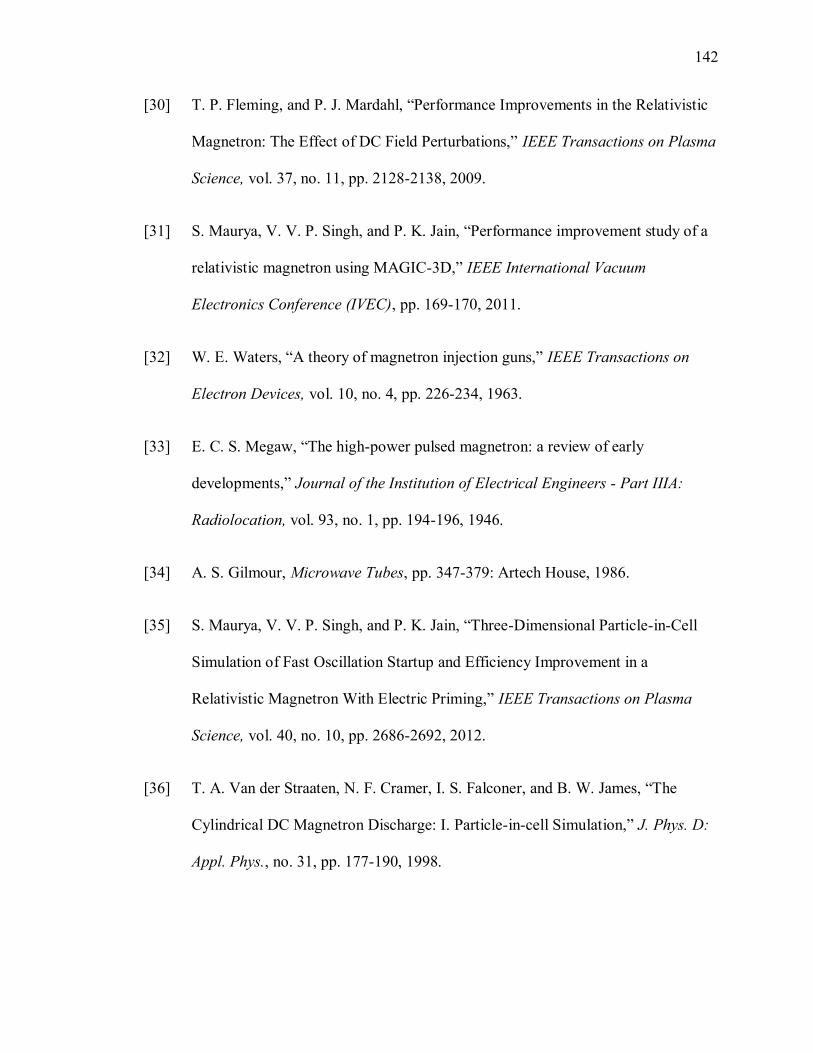
142
[30] T. P. Fleming, and P. J. Mardahl, “Performance Improvements in the Relativistic
Magnetron: The Effect of DC Field Perturbations,” IEEE Transactions on Plasma
Science, vol. 37, no. 11, pp. 2128-2138, 2009.
[31] S. Maurya, V. V. P. Singh, and P. K. Jain, “Performance improvement study of a
relativistic magnetron using MAGIC-3D,” IEEE International Vacuum
Electronics Conference (IVEC), pp. 169-170, 2011.
[32] W. E. Waters, “A theory of magnetron injection guns,” IEEE Transactions on
Electron Devices, vol. 10, no. 4, pp. 226-234, 1963.
[33] E. C. S. Megaw, “The high-power pulsed magnetron: a review of early
developments,” Journal of the Institution of Electrical Engineers - Part IIIA:
Radiolocation, vol. 93, no. 1, pp. 194-196, 1946.
[34] A. S. Gilmour, Microwave Tubes, pp. 347-379: Artech House, 1986.
[35] S. Maurya, V. V. P. Singh, and P. K. Jain, “Three-Dimensional Particle-in-Cell
Simulation of Fast Oscillation Startup and Efficiency Improvement in a
Relativistic Magnetron With Electric Priming,” IEEE Transactions on Plasma
Science, vol. 40, no. 10, pp. 2686-2692, 2012.
[36] T. A. Van der Straaten, N. F. Cramer, I. S. Falconer, and B. W. James, “The
Cylindrical DC Magnetron Discharge: I. Particle-in-cell Simulation,” J. Phys. D:
Appl. Phys., no. 31, pp. 177-190, 1998.

143
[37] C. Xiaodong, M. Esterson, and P. A. Lindsay, “Computer simulation of a high-
power magnetron and the possible implications for RF pulse shortening,” IEEE
Transactions on Plasma Science, vol. 26, no. 3, pp. 726-732, 1998.
[38] K. Posthumous, “Oscillations in a Split-Anode Magnetron,” Wireless Engineer,
no. 12, pp. 126-132, 1935.
[39] A. L. Samuel, Magnetron, Electron Discharge Device, U.S. Patent 2,063,342,
1934.
[40] N. T. Aleksereff, and D. E. Malearoff, “Generation of High Power Oscillations
with a Magnetron in the Centimeter Band,” Journal of Technical Physics USRR,
vol. 10, pp. 1297, 1940.
[41] A. D. Andreev, and K. J. Hendricks, “First multi-cavity magnetrons were built in
NII-9, Leningrad, during the spring of 1937 PIC simulations of the first 4-cavity
S-band CW magnetron,” International Conference on the Origins and Evolution
of the Cavity Magnetron (CAVMAG), pp. 71-75, 2010.
[42] W. Arter, and J. Eastwood, “The modelling of relativistic magnetrons,” IEE
Seminar Digests, vol. 1997, no. 374, pp. 3-3, 1997.
[43] N. I. Avtomonov, S. V. Sosnytskiy, and D. M. Vavriv, “Operating Modes of
Magnetron Auxiliary Cathode,” The Sixth International Kharkov Symposium on
Physics and Engineering of Microwaves, Millimeter and Submillimeter Waves
and Workshop on Terahertz Technologies., vol. 2, pp. 547-549, 2007.

144
[44] M. A. Kopot, V. D. Yeryomka, and V. P. Dzyuba, “3-B Simulation of
Magnetrons Having a Secondary-Emission Cathode Stimulated by Electrons from
a Field Emitter,” IEEE International Vacuum Electronics Conference (IVEC), pp.
351-353, 2006.
[45] M. Leconte, “A statistical study of magnetron patents in the early years of
electronics between 1920 and 1945; heuristic foucusing around the discovery of
the cavity magnetron,” International Conference on the Origins and Evolution of
the Cavity Magnetron (CAVMAG), pp. 11-16, 2010.
[46] P. A. Redhead, “The Invention of the Cavity Magnetron and its Introduction into
Canada and the U.S.A.,” La Physique Au Canada, novembre/decembre, pp. 321-
328, 2001.
[47] J. Zhang, X. Chen, M. Esterson, P. Lindsay, P. Burleigh, and D. Wilson, “3D
computer modelling of phase control in a magnetron through the output system,”
IEEE International Conference on Plasma Science, pp. 411-411, 2006.
[48] H. A. H. Boot, and J. T. Randall, “Historical Notes on the Cavity Magnetron,”
IEEE Transactions on Electron Devices, vol. 23, no. 7, pp. 724-729, 1976.
[49] T. J. Davis, “Toward a Viable High-Power Coaxial Microwave Source,” School
of Electrical Engineering, Cornell University, 1993.
[50] S. Dushman, “Electron emission,” Electrical Engineering, vol. 53, pp. 1054-1062,
1934.
145
[51] D. A. Shiffler, M. Ruebush, D. Zagar, M. LaCour, K. Golby, M. Collins, M.
Haworth, and R. Umstattd, “Emission Uniformity and Emittance of Explosive
Fiel-Emission Cathodes,” IEEE Transactions on Plasma Science, vol. 30, no. 4,
pp. 1592-1596, 2002.
[52] W. M. White, “RF Priming of a Long Pulse Relativistic Magnetron ”, Nuclear
Engineering and Radiological Sciences, University of Michigan, Ann Arbor,
Michigan, 2006.
[53] Y. M. Saveliev, B. A. Kerr, M. I. Harbour, S. C. Douglas, and W. Sibbett,
“Operation of a relativistic rising-sun magnetron with cathodes of various
diameters,” IEEE Transactions on Plasma Science, vol. 30, no. 3, pp. 938-946,
2002.
[54] Y. M. Saveliev, S. N. Spark, B. A. Kerr, M. I. Harbour, S. C. Douglas, and W.
Sibbett, “New cathodes for a relativistic magnetron,” Proceedings of the 12th
International Conference on High-Power Particle Beams, vol. 2, pp. 861-864
vol.2, 1998.
[55] W. M. White, R. M. Gilgenbach, M. C. Jones, V. B. Neculaes, L. Yue Ying, P.
Pengvanich, N. M. C. Jordan, B. W. Hoff, R. Edgar, T. A. Spencer, and D. Price,
“Radio frequency priming of a long-pulse relativistic magnetron,” IEEE
Transactions on Plasma Science, vol. 34, no. 3, pp. 627-634, 2006.
[56] W. E. Willshaw, L. Rushforth, A. G. Stainsby, R. Latham, A. W. Balls, and A. H.
King, “The high-power pulsed magnetron: development and design for radar
146
applications,” Journal of the Institution of Electrical Engineers - Part IIIA:
Radiolocation, vol. 93, no. 5, pp. 985, 1946.
[57] V. Bagad, Microwave Engineering - I, First ed., Pune, India: Technical
Publications Pune, 2009.
[58] L. Ma, “3D Computer Modeling of Magnetrons,” Department of Electronic
Engineering, Queen Mary, University of London, United Kingdom, 2004.
[59] O. Bunemann, “A Small Amplitude Theory for Magnetrons,” Journal of
Electronics and Control, pp. 1-50, 1957.
[60] W. Knauer, “Diocotron Instability in Plasmas and Gas Discharges,” Journal of
Applied Physics, vol. 37, no. 2, pp. 602-611, 1965.
[61] S. Millman, and A. T. Nordsieck, “The Rising Sun Magnetron,” Journal of
Applied Physics, vol. 19, no. 2, pp. 156-165, 1948.
[62] N. M. Kroll, and J. W. E. Lamb, “The Resonant Modes of the Rising Sun and
Other Unstrapped Magnetron Anode Blocks,” Journal of Applied Physics, vol. 19,
no. 2, pp. 166-186, 1948.
[63] A. V. Hollenberg, N. Kroll, and S. Millman, “Rising Sun Magnetrons with Large
Numbers of Cavities,” Journal of Applied Physics, vol. 19, no. 7, pp. 624-635,
1948.
[64] "Ostron Technologies," http://www.ostron.de/.

147
[65] A. C. Dexter, G. Burt, R. G. Carter, I. Tahir, H. Wang, K. Davis, and R. Rimmer,
“First demonstration and performance of an injection locked continuous wave
magnetron to phase control a superconducting cavity,” Physical Review Special
Topics - Accelerators and Beams, vol. 14, no. 3, pp. 032001, 2011.
[66] R. Adler, “A Study of Locking Phenomena in Oscillators,” Proceedings of the
IRE, vol. 61, no. 10, pp. 1380-1385, 1946.
[67] E. E. David, "Locking Phenomena in Microwave Oscillators," Research
Laboratory of Electronics, Massachusetts Institute of Technology, 1948.
[68] E. J. Cruz, B. W. Hoff, P. Pengvanich, Y. Y. Lau, R. M. Gilgenbach, and J. W.
Luginsland, “Experiments on peer-to-peer locking of magnetrons,” Applied
Physics Letters, vol. 95, no. 19, pp. 191503-3, 2009.
[69] M. C. Jones, V. B. Neculaes, Y. Y. Lau, R. M. Gilgenbach, and W. M. White,
“Cathode priming of a relativistic magnetron,” Applied Physics Letters, vol. 85,
no. 26, pp. 6332-6334, 2004.
[70] V. B. Neculaes, “Magnetron magnetic Priming for Rapid Startup and Noise
Reduction,” Nuclear Science, University of Michigan, 2005.
[71] C. Mendonca, S. Prasad, E. Schamiloglu, and T. Fleming, “3D ICEPIC
simulations of a pulsed relativistic magnetron with transparent cathode: A
comparative study,” IEEE Pulsed Power Conference (PPC), pp. 823-828, 2011.
148
[72] D. A. Shiffler, M. Ruebush, M. LaCour, K. Golby, R. Umstattd, M. C. Clark, J.
W. Luginsland, D. Zagar, and M. Sena, “Emission Uniformity and Emission Area
of Explosive Field Emission Cathodes,” Applied Physics Letters, vol. 79, no. 18,
pp. 2871-2873, 2001.
[73] D. Whaley, R. Duggal, and C. Armstrong, “100 W Operation of a Cold Cathode
TWT,” IEEE Transactions on Electron Devices, vol. 56, no. 5, pp. 896-905, 2009.
[74] D. Whaley, B. Gannon, V. Heinen, K. Kreischer, C. Holland, and C. Spindt,
“Experimental Demonstration of an Emission-Gated Traveling-Wave Tube
Amplifier,” IEEE Transactions on Plasma Science, vol. 30, no. 3, 2002.
[75] C. K. Birdsall, and A. B. Langdon, Plasma Physics Via Computer Simulation:
McGraw-Hill, 1985.
[76] C. Nieter, and J. R. Cary, “VORPAL: a versatile plasma simulation code,”
Journal of Computational Physics, vol. 196, no. 2, pp. 448-473, 2004.
[77] M. C. Lin, C. Nieter, P. H. Stoltz, and D. Smithe, “Accurately and Efficiently
Studying the RF Structures Using a Conformal Finite-Difference Time-Domain
Particle-in-Cell Method,” The Open Plasma Physics Journal, vol. 3, pp. 48-52,
2010.
[78] R. W. Lemke, “3D PIC simulation study of the relativistic magnetron,” IEEE
International Conference on Plasma Science, pp. 206, 1998.

149
[79] B. W. Hoff, M. Franzi, R. M. Gilgenbach, and Y. Y. Lau, “Three-Dimensional
Simulations of Magnetic Priming of a Relativistic Magnetron,” IEEE
Transactions on Plasma Science, vol. 38, no. 6, pp. 1292-1301, 2010.
[80] X. Chen, M. Esterson, and P. A. Lindsay, “3D simulation of microwave
magnetrons,” IEE Colloquium on High Frequency Simulation: Part Two, pp. 1/1-
1/4, 1997.
[81] J. W. Eastwood, and W. Arter, “3D PIC simulation of relativistic magnetrons,”
International Vacuum Electronics Conference, pp. 1-2, 2000.
[82] C. Nieter, J. R. Cary, D. Smithe, P. H. Stoltz, and G. R. Werner, “Simulations of
Electron Effects in Superconducting Cavities with the Vorpal Code,” 10th
European Particle Accelerator Conference, pp. 2269-2271, 2006.
[83] C. Nieter, J. R. Cary, G. R. Werner, D. Smithe, and P. H. Stoltz, “Application of
Dey-Mittra Conformal Boundary Algorithm to 3D Electromagnetic Modeling,”
Journal of Computational Physics, no. 228, pp. 7902-7916, 2009.
[84] K. S. Yee, “Numerical Solution of Initial Boundary Value Problems Involving
Maxwell's Equations in Isotropic Media,” IEEE Transactions on Antennas and
Propagation, vol. AP-14, no. 3, pp. 302-307, 1966.
[85] K. S. Kunz, and R. J. Luebbers, The Finite Difference Time Domain Method for
Electromagnetics, pp. 429: CRC Press, 2000.
150
[86] D. M. Sullivan, Electromagnetic Simulation Using the FDTD Method, pp. 336,
2000.
[87] R. Courant, K. Friedrichs, and H. Lewy, “On the Partial Difference Equations of
Mathematical Physics,” IBM Journal, March, 1967.
[88] A. C. Cangellaris, and D. B. Wright, “Analysis of the Numerical Error Caused by
the Stair-stepped Approximation of a Conducting Boundary in FDTD Simulations
of Electromagnetic Phenomena,” IEEE Transactions on Antennas and
Propagation, vol. 39, pp. 1518-1525, 1991.
[89] S. Dey, and R. Mittra, “A Locally Conformal Finite-Difference Time-Domain
(FDTD) Algorithm for Modeling Three-Dimensional Perfectly Conducting
Objects,” IEEE Microwave and Guided Wave Letters, vol. 7, no. 9, pp. 273-275,
1997.
[90] R. Schuhmann, T. Weiland, and I. A. Zagorodnov, “A Uniformaly Stable
Conformal FDTD-method in Cartesian Grids,” International Journal of
Numerical Modeling, vol. 16, pp. 127, 2003.
[91] C. S. Technology. "3D EM Simulations: Methods for Loaded Q Calculations,"
www.cst-world.com.
[92] A. Wolski, "Cavities and Waveguides," Physical Review Special Topics, 2007.
[93] M. C. Lin, P. H. Stoltz, D. Smithe, H. Song, H. Jong, J. J. Choi, S. J. Kim, and S.
H. Jang, “Design and Modeling of Multistate Depressed Collectors by Using,”

151
Journal of the Korean Physical Society, vol. 60, no. 5, pp. 731-738, March 2012,
2012.
[94] S. G. Bandy, C. Spindt, M. A. Hollis, W. D. Palmer, B. Goplen, and E. G.
Wintucky, “Application of Gated Field Emitter Arrays in Microwave Amplifier
Tubes,” in Vacuum Microelectronics Conference, 1998, pp. 132-133.
[95] C. Spindt, C. Holland, and I. Schwoebel, “Field-Emitter-Array Development for
Microwave Applications,” in Electron Devices Meeting, IEDM '95, Washington,
DC, 1995, pp. 389-392.
[96] D. Whaley, B. Gannon, C. R. Smith, C. Armstrong, and C. Spindt, “Application
of Field Emitter Arrays to Microwave Power Amplifiers,” IEEE Transactions on
Plasma Science, vol. 28, no. 3, pp. 727-746, 2000.
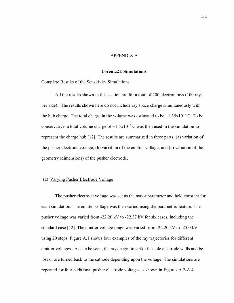
152
APPENDIX A
Lorentz2E Simulations
Complete Results of the Sensitivity Simulations
All the results shown in this section are for a total of 200 electron rays (100 rays
per side). The results shown here do not include ray space charge simultaneously with
the hub charge. The total charge in the volume was estimated to be −1.35x10⁻⁸
C. To be
conservative, a total volume charge of −1.5x10⁻⁸
C was then used in the simulation to
represent the charge hub [12]. The results are summarized in three parts: (a) variation of
the pusher electrode voltage, (b) variation of the emitter voltage, and (c) variation of the
geometry (dimensions) of the pusher electrode.
(a) Varying Pusher Electrode Voltage
The pusher electrode voltage was set as the major parameter and held constant for
each simulation. The emitter voltage was then varied using the parametric feature. The
pusher voltage was varied from -22.20 kV to -22.37 kV for six cases, including the
standard case [12]. The emitter voltage range was varied from -22.20 kV to -25.0 kV
using 20 steps. Figure A.1 shows four examples of the ray trajectories for different
emitter voltages. As can be seen, the rays begin to strike the sole electrode walls and be
lost or are turned back to the cathode depending upon the voltage. The simulations are
repeated for four additional pusher electrode voltages as shown in Figures A.2-A.4.

153
(a.1) Pusher electrode at -22.20 kV
(a) (b)
(c) (d)
Figure A.1: Pusher Electrode Voltage at -22.20 kV. Emitter Voltage at
(a) -22.20kV, (b) -22.26 kV, (c) -22.34 kV, and (d) -22.5 kV.
(a.2) Pusher electrode at -22.26 kV
(a) (b)
(c) (d)
Figure A.2: Pusher Electrode Voltage at -22.26 kV. Emitter Voltage at
(a) -22.20kV, (b) -22.26 kV, (c) -22.34 kV, and (d) -22.5 kV.

154
(a.3) Pusher electrode at -22.30 kV
(a) (b)
(c) (d)
Figure A.3: Pusher Electrode Voltage at -22.30 kV. Emitter Voltage at
(a) -22.20kV, (b) -22.26 kV, (c) -22.34 kV, and (d) -22.5 kV.
(a.4) Pusher electrode at -22.37 kV
(a) (b)
(c) (d)
Figure A.4: Pusher Electrode Voltage at -22.37 kV. Emitter Voltage at
(a) -22.20 kV, (b) -22.26 kV (c), -22.34 kV, and (d) -22.5 kV.

155
(a.5) Collector Current Analysis
A diagnostic was placed at the collector to measure the current (number of rays),
which exit the slit and strike the collector. In Figure A.5, a plot of the ratio of Iout/Iin vs.
emitter voltage is graphed for the five pusher electrode cases. Iout and Iin are the collector
current and emitter current, respectively. The threshold for the maximum current out was
set equal or greater to 90% (this threshold was taken into account for the following
cases). The threshold value was determined considering that there are a small percentage
of rays that do not come out. This amount of rays was calculated to be approximately
between 10-20 rays in total. This amount of emitter current loss (injected emitter current)
was calculated and subtracted from the original injected emitter current. The voltage
sensitivity (ΔV) was calculated for this threshold value. These results are shown in Table
4.1A.1. This means that the resulting ΔV calculated for each case shows how sensitive
the emitters are to the parameter changes. A large ΔV indicates low sensitivity to voltage
variation, which is desirable for device operation.

156
Figure A.5: Emitter voltage versus current ratio.
Table A.1: Voltage sensitivity analysis results for variations in the pusher
electrode voltage.
Pusher electrode
voltage (kV)
Maximum current
out (%)
ΔV (V)
-22.29 97.2% 78.95
-22.30 98.3% 110.5
-22.31 98.3% 102.3
-22.37 98.3% 189.5
(b) Varying Emitter Voltage
The emitter voltage was set as a major parameter with the pusher electrode
voltage varied by the parametric function. The emitter voltage was varied from -22.20 kV
to -22.37 kV in six cases, including the standard case [12]. The pusher electrode voltage
was varied from -22.20 kV to -25.0 kV using 20 steps. Figures A.5-A.8 show the results
of the ray trajectories at different pusher electrode voltages with a fixed emitter voltage.

157
(b.1) Emitter voltage at -22.20 kV
(a) (b)
(c) (d)
Figure A.5: Emitter Voltage at -22.20 kV. Pusher Electrode Voltage at
(a) -22.20 kV, (b) -22.26 kV, (c) -22.34 kV, and (d) -22.5 kV.
(b.2) Emitter voltage at -22.26 kV
(a) (b)
(c) (d)
Figure A.6: Emitter Voltage at -22.26 kV. Pusher Electrode Voltage at
(a) -22.20 kV, (b) -22.26 kV, (c) -22.34 kV, and (d) -22.5 kV.

158
(b.3) Emitter voltage at -22.30 kV
(a) (b)
(c) (d)
Figure A.7: Emitter Voltage at -22.30 kV. Pusher Electrode Voltage at
(a) -22.20 kV, (b) -22.26 kV, (c) -22.34 kV, and (d) -22.5 kV.
(b.4) Emitter voltage at -22.37 kV
(a) (b)
(c) (d)
Figure A.8: Emitter Voltage at -22.37 kV. Pusher Electrode Voltage at
(a) -22.20 kV, (b) -22.26 kV, (c) -22.34 kV, and (d) -22.5 kV.

159
(b.5) Collector current analysis
A diagnostic was placed at the collector to measure the current at which the rays
will hit the collector. In Figure A.9, a plot of the pusher electrode voltage vs. the rate of
Iout/Iin at the different emitter voltages studied in the previous section is presented. The
voltage sensitivity (ΔV) was calculated and is presented in Table A.2.
Figure A.9: Pusher Electrode Voltage vs. Current Ratio.
Table A.2: Voltage sensitivity analysis results for variations in the emitter
voltage.
Emitter voltage
(kV)
Maximum current
out (%)
ΔV (V)
-22.26 91.1% 63.15
-22.29 97.2% 78.95
-22.30 97.8% 94.74
-22.31 97.2% 126.3
-22.37 98.3% 157.9

160
(c) Varying the geometry
In this section, the simulation results are from the variation of the geometry of the
pusher electrode; the simulations shown in section (a) and (b) were repeated for each
geometry. The pusher electrode has a thickness of 0.9795 µm from the reference model
studied in [12]. This thickness was modified to its maximum and minimum to study the
device sensitivity due to changing the geometry. The simulations are performed for two
different pusher electrode thicknesses: geometry (1) corresponds to a thickness of 1.70
µm and geometry (2) corresponds to a thickness of 0.4475 µm. These results are
presented in Figures A.10-A.19 for the 1.70 um case and in Figures A.20-A.28 for the
0.4475 um case. These results clearly show an improvement in the extracted current by
moving the pusher electrode closer (vertically) to the emitter.
(c.1) Geometry (1) 1.70 µm thick, varying pusher electrode voltage
(c.1.1) Pusher electrode voltage at -22.20 kV
(a) (b)
(c) (d)
Figure A.10: Pusher Electrode Voltage at -22.20 kV. Emitter Voltage at
(a) -22.20 kV, (b) -22.26 kV, (c) -22.34 kV, and (d) -22.5 kV.

161
(c.1.2) Pusher electrode voltage at -22.26 kV
(a) (b)
(c) (d)
Figure A.11: Pusher Electrode Voltage at -22.26 kV. Emitter Voltage at
(a) -22.20 kV, (b) -22.26 kV, (c) -22.34 kV, and (d) -22.5 kV.
(c.1.3) Pusher electrode voltage at -22.30 kV
(a) (b)
(c) (d)
Figure A.12: Pusher Electrode Voltage at -22.30 kV. Emitter Voltage at
(a) -22.20 kV, (b) -22.26 kV, (c) -22.34 kV, and (d) -22.5 kV.
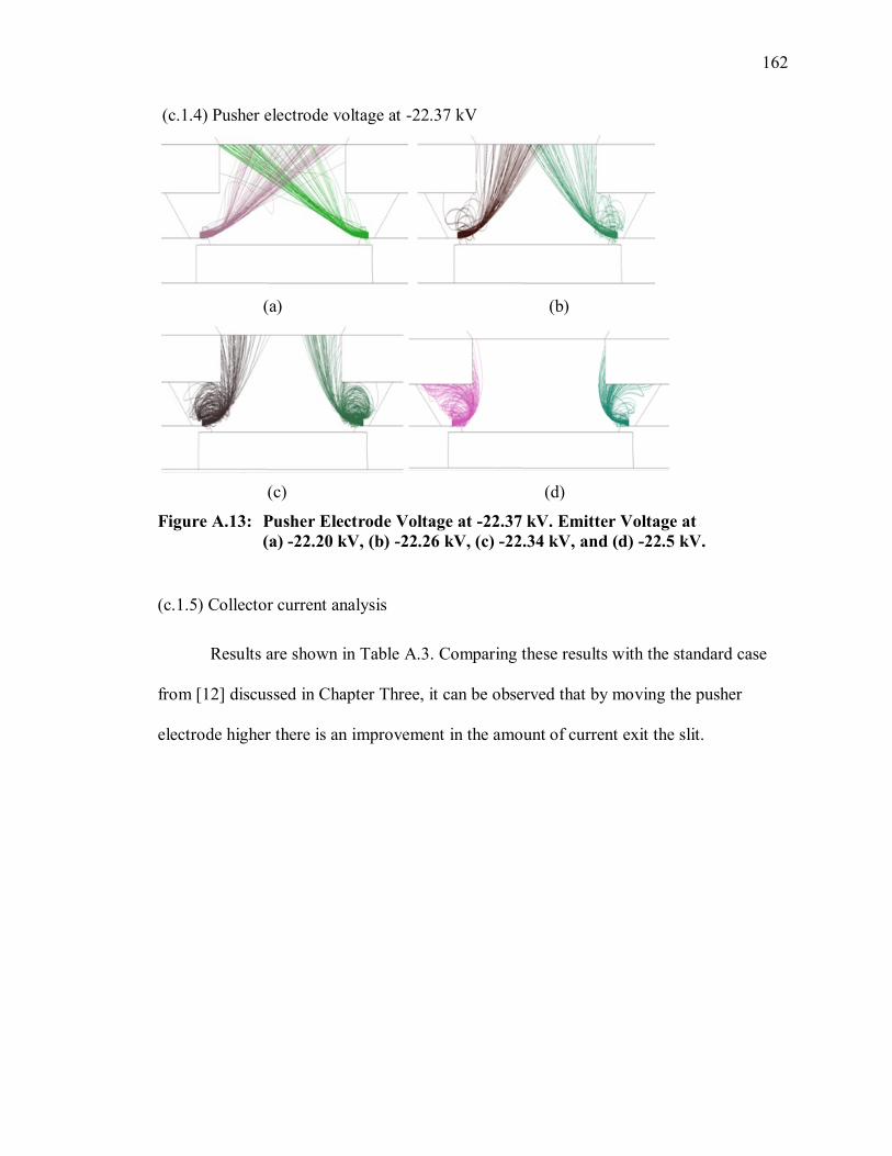
162
(c.1.4) Pusher electrode voltage at -22.37 kV
(a) (b)
(c) (d)
Figure A.13: Pusher Electrode Voltage at -22.37 kV. Emitter Voltage at
(a) -22.20 kV, (b) -22.26 kV, (c) -22.34 kV, and (d) -22.5 kV.
(c.1.5) Collector current analysis
Results are shown in Table A.3. Comparing these results with the standard case
from [12] discussed in Chapter Three, it can be observed that by moving the pusher
electrode higher there is an improvement in the amount of current exit the slit.
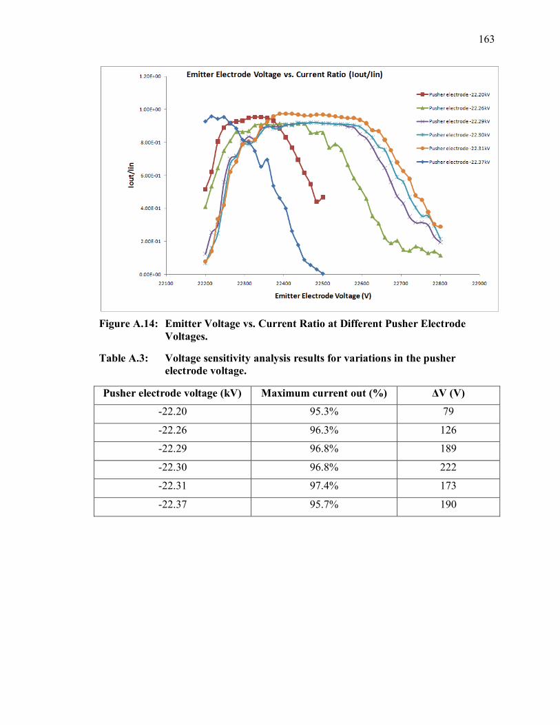
163
Figure A.14: Emitter Voltage vs. Current Ratio at Different Pusher Electrode
Voltages.
Table A.3: Voltage sensitivity analysis results for variations in the pusher
electrode voltage.
Pusher electrode voltage (kV) Maximum current out (%) ΔV (V)
-22.20 95.3% 79
-22.26 96.3% 126
-22.29 96.8% 189
-22.30 96.8% 222
-22.31 97.4% 173
-22.37 95.7% 190
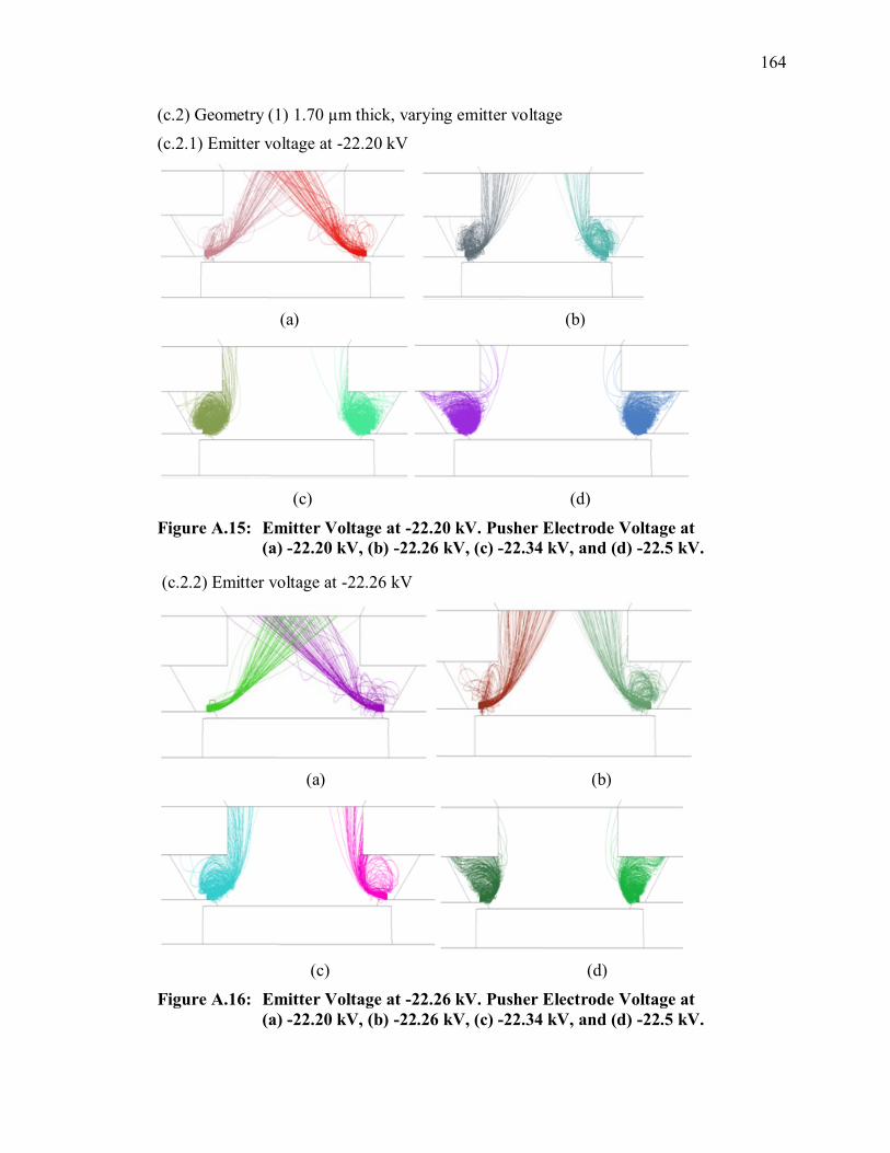
164
(c.2) Geometry (1) 1.70 µm thick, varying emitter voltage
(c.2.1) Emitter voltage at -22.20 kV
(a) (b)
(c) (d)
Figure A.15: Emitter Voltage at -22.20 kV. Pusher Electrode Voltage at
(a) -22.20 kV, (b) -22.26 kV, (c) -22.34 kV, and (d) -22.5 kV.
(c.2.2) Emitter voltage at -22.26 kV
(a) (b)
(c) (d)
Figure A.16: Emitter Voltage at -22.26 kV. Pusher Electrode Voltage at
(a) -22.20 kV, (b) -22.26 kV, (c) -22.34 kV, and (d) -22.5 kV.

165
(c.2.3) Emitter voltage at -22.30 kV
(a) (b)
(c) (d)
Figure A.17: Emitter Voltage at -22.30 kV. Pusher Electrode Voltage at
(a) -22.20 kV, (b) -22.26 kV, (c) -22.34 kV, and (d) -22.5 kV.
(c.2.4) Emitter voltage at -22.37 kV
(a) (b)
(c) (d)
Figure A.18: Emitter Voltage at -22.37 kV. Pusher Electrode Voltage at
(a) -22.20 kV, (b) -22.26 kV, (c) -22.34 kV, and (d) -22.5 kV.

166
(c.2.5) Collector current analysis
Results are shown in Table A.4. Comparing these results with the standard case
from [12] discussed in Chapter Three, it can be observed that by moving the pusher
electrode higher the amount of current out the slit is improved.
Figure A.19: Pusher Electrode Voltage vs. Current Ratio at Different Emitter
Voltages.
Table A.4: Voltage sensitivity analysis results for variations in the emitter
voltage.
Emitter voltage (kV) Maximum current out (%) ΔV (V)
-22.26 92.1% 113
-22.29 95.3% 90
-22.30 95.8% 90
-22.31 96.3% 90
-22.37 96.3% 110.5
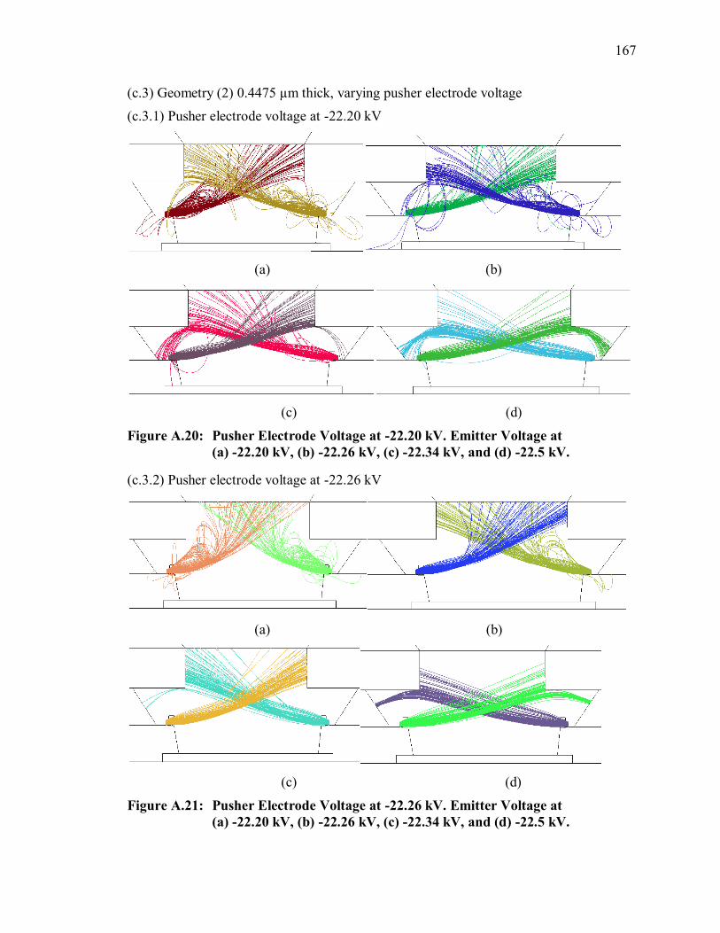
167
(c.3) Geometry (2) 0.4475 µm thick, varying pusher electrode voltage
(c.3.1) Pusher electrode voltage at -22.20 kV
(a) (b)
(c) (d)
Figure A.20: Pusher Electrode Voltage at -22.20 kV. Emitter Voltage at
(a) -22.20 kV, (b) -22.26 kV, (c) -22.34 kV, and (d) -22.5 kV.
(c.3.2) Pusher electrode voltage at -22.26 kV
(a) (b)
(c) (d)
Figure A.21: Pusher Electrode Voltage at -22.26 kV. Emitter Voltage at
(a) -22.20 kV, (b) -22.26 kV, (c) -22.34 kV, and (d) -22.5 kV.

168
(c.3.3) Pusher electrode voltage at -22.30 kV
(a) (b)
(c) (d)
Figure A.22: Pusher Electrode Voltage at -22.30 kV. Emitter Voltage at
(a) -22.20 kV, (b) -22.26 kV, (c) -22.34 kV, and (d) -22.5 kV.
(c.3.4) Pusher electrode voltage at -22.37 kV
(a) (b)
(c) (d)
Figure A.23: Pusher Electrode Voltage at -22.37 kV. Emitter Voltage at
(a) -22.20 kV, (b) -22.26 kV, (c) -22.34 kV, and (d) -22.5 kV.
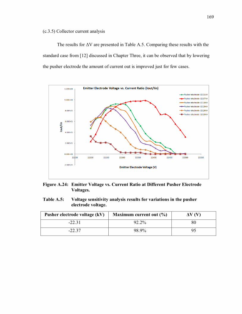
169
(c.3.5) Collector current analysis
The results for ΔV are presented in Table A.5. Comparing these results with the
standard case from [12] discussed in Chapter Three, it can be observed that by lowering
the pusher electrode the amount of current out is improved just for few cases.
Figure A.24: Emitter Voltage vs. Current Ratio at Different Pusher Electrode
Voltages.
Table A.5: Voltage sensitivity analysis results for variations in the pusher
electrode voltage.
Pusher electrode voltage (kV) Maximum current out (%) ΔV (V)
-22.31 92.2% 80
-22.37 98.9% 95
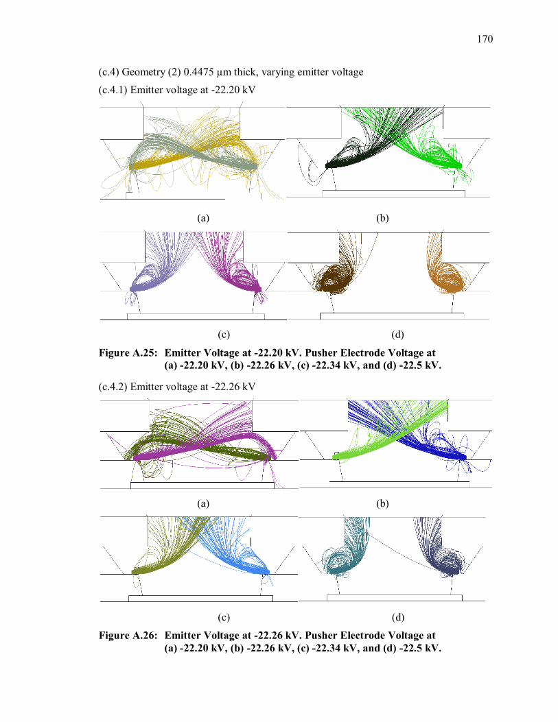
170
(c.4) Geometry (2) 0.4475 µm thick, varying emitter voltage
(c.4.1) Emitter voltage at -22.20 kV
(a) (b)
(c) (d)
Figure A.25: Emitter Voltage at -22.20 kV. Pusher Electrode Voltage at
(a) -22.20 kV, (b) -22.26 kV, (c) -22.34 kV, and (d) -22.5 kV.
(c.4.2) Emitter voltage at -22.26 kV
(a) (b)
(c) (d)
Figure A.26: Emitter Voltage at -22.26 kV. Pusher Electrode Voltage at
(a) -22.20 kV, (b) -22.26 kV, (c) -22.34 kV, and (d) -22.5 kV.

171
(c.4.3) Emitter voltage at -22.30 kV
(a) (b)
(c) (d)
Figure A.27: Emitter Voltage at -22.30 kV. Pusher Electrode Voltage at
(a) -22.20 kV, (b) -22.26 kV, (c) -22.34 kV, and (d) -22.5 kV.
(c.4.4) Emitter voltage at -22.37 kV
(a) (b)
(c) (d)
Figure A.28: Emitter Voltage at -22.37 kV. Pusher Electrode Voltage at
(a) -22.20 kV, (b) -22.26 kV, (c) -22.34 kV, and (d) -22.5 kV.

172
(c.4.5) Collector current analysis
The results for ΔV are presented in Table A.6. Comparing these results with the
standard case from [12] discussed in Chapter Three, it can be observed that by lowering
the pusher electrode the amount of current out is improved just for few cases.
Figure A.29: Pusher Electrode Voltage vs. Current Ratio at Different Emitter
Voltages.
Table A.6: Voltage sensitivity analysis results for variations in the emitter
voltage.
Emitter voltage (kV) Maximum current out (%) ΔV (V)
-22.29 97.2% 95
-22.30 97.8% 110.5
-22.31 96.1% 130
-22.37 98.9% 200

173
APPENDIX B
VORPAL Simulation Input Decks
Continuous Current Source Model
$ import mathphys.mac
$ import geometry.mac
$ import mal.mac
# units
$ CM = 1.0e-2
$ NANOSECONDS = 1.0e-9
$ GIGAHERTZ = 1.0e9
$ METER = 1.0
$ SECONDS = 1.0
$ VOLTS = 1.0
$ AMPS = 1.0
$ TESLA = 1.0
$ DEGREES = PI/180.0
# - - - - - - - - - - - - - - - - - - - - - - - - - - - - - - - - - - - - - - - - - - - - - - - - - - - - - - - - - - - -
# - - - - - - - - - - - - - - - - - - - - - - - - - - - - - - - - - - - - - - - - - - - - - - - - - - - - - - - - - - - -
#
# ___ TYPICAL TYPES OF RUNS ___
# 1) to determine the mode spectrum, set: IMPULSE_EXCITATION=1,
PI_MODE_PRIMING=0, INCLUDE_DC_VOLTAGE=0, INCLUDE_PARTICLES=0
# 2) to calibrate the pi-mode frequency and Q, set: IMPULSE_EXCITATION=0,
PI_MODE_PRIMING=1, INCLUDE_DC_VOLTAGE=0, INCLUDE_PARTICLES=0
# 3) to calibrate DC voltage, set: IMPULSE_EXCITATION=0,
PI_MODE_PRIMING=0, INCLUDE_DC_VOLTAGE=1, INCLUDE_PARTICLES=0
# 4) to perform an actual run, set: IMPULSE_EXCITATION=0,
PI_MODE_PRIMING=0, INCLUDE_DC_VOLTAGE=1, INCLUDE_PARTICLES=1
#
# You may also include IMPULSE_EXCITATION or PI_MODE_PRIMING in an actual
run, to try to get a faster turnon.
#
# - - - - - - - - - - - - - - - - - - - - - - - - - - - - - - - - - - - - - - - - - - - - - - - - - - - - - - - - - - - -
- - - - - - -
# IMPULSE EXCITATION CONTROL
$ IMPULSE_EXCITATION = 0
# PI MODE PRIMING CONTROL

174
$ PI_MODE_PRIMING = 0
# DC VOLTAGE CONTROL
$ INCLUDE_DC_VOLTAGE = 1
# PARTICLES CONTROL
$ INCLUDE_PARTICLES = 1
# SIMULATION RUN TIME CONTROL
$ RISETIME = 1.0*NANOSECONDS
$ RUNTIME = 600.0*NANOSECONDS
$ NUMBER_OF_DUMPS = 50
# - - - - - - - - - - - - - - - - - - - - - - - - - - - - - - - - - - - - - - - - - - - - - - - - - - - - - - - - - - - -
# 2D Rising Sun Magnetron geometry parameters
# ... the first-of-the-NCAVITY CAVITY1's is centered on the positive X axis
$ PENTAGON_CATHODE = 0
$ RCATHODE = 1.000*CM
$ RANODE = 2.242*CM
$ RCAVITY1 = 10.000*CM
$ RCAVITY2 = 6.000*CM
$ ANGLECAVITY1 = 10.0*DEGREES
$ ANGLECAVITY2 = 10.0*DEGREES
$ NCAVITY = 5
# Magnetron cavity loading parameter, controls Q, which goes as 1/NU_LOADING
$ NU_LOADING = 200.0e6/SECONDS
# Magnetron operating parameters
$ VOLTAGE_DC = 26.0e3*VOLTS
$ EMITTED_CURRENT = 500.0*AMPS/METER
$ BSTATIC = 0.12*TESLA
# - - - - - - - - - - - - - - - - - - - - - - - - - - - - - - - - - - - - - - - - - - - - - - - - - - - - - - - - - - - -
# WORKSHEET
# In a magnetron, the DC_VOLTAGE must be above the Hartree voltage, which is given
by
$ HARTREE_MODE_FREQ = 0.96*GIGAHERTZ
$ HARTREE_MODE_PHIDOT = TWOPI*HARTREE_MODE_FREQ/NCAVITY
$ HARTREE_VDRIFT_SPOKE =
0.5*(RANODE+RCATHODE)*HARTREE_MODE_PHIDOT
$ HARTREE_VDRIFT_ANODE = RANODE*HARTREE_MODE_PHIDOT
$ HARTREE_VOLTAGE = BSTATIC*(RANODE-
RCATHODE)*HARTREE_VDRIFT_SPOKE -
0.5*ELECMASS*HARTREE_VDRIFT_ANODE**2/ELEMCHARGE
# uncomment this line to print out HARTREE_VOLTAGE
# - - - - - - - - - - - - - - - - - - - - - - - - - - - - - - - - - - - - - - - - - - - - - - - - - - - - - - - - - - - -
- - - - - - -
# Simulation Domain Size, at least a cell larger than any structure
$ LX = 20.4*CM
$ LY = 20.4*CM
$ XBGN = -0.5*LX
$ YBGN = -0.5*LY

175
$ XEND = XBGN + LX
$ YEND = YBGN + LY
# Grid
$ NX = 102
$ NY = 102
$ NZ = 1
$ DX = LX/NX
$ DY = LY/NY
# Time parameters, apply Dey-Mittra Courant condition
$ DM_FRAC = 0.5
$ DT = 0.98*DM_FRAC/LIGHTSPEED/math.sqrt(1.0/(DX*DX)+1.0/(DY*DY))
$ TIMESTEPS = int(RUNTIME/DT)
$ NSTEPSPERDUMP = int(TIMESTEPS/NUMBER_OF_DUMPS)
# anode geometry function
<function solid_anode(x,y)>
H(RANODE^2-x^2-y^2)-0.4
</function>
$ DPHI = TWOPI/NCAVITY
<function wrapped_angle1(x,y)>
mod(atan2(y,x)+TWOPI+0.5*DPHI,DPHI)-0.5*DPHI
</function>
<function wrapped_angle2(x,y)>
mod(atan2(y,x)+TWOPI+1.0*DPHI,DPHI)-0.5*DPHI
</function>
<function cavities1(x,y)>
H(0.5*ANGLECAVITY1-abs(wrapped_angle1(x,y)))*H(x^2+y^2-
RANODE^2)*H(RCAVITY1^2-x^2-y^2)-0.4
</function>
<function cavities2(x,y)>
H(0.5*ANGLECAVITY2-abs(wrapped_angle2(x,y)))*H(x^2+y^2-
RANODE^2)*H(RCAVITY2^2-x^2-y^2)-0.4
</function>
<function anode(x,y)>
max(max(solid_anode(x,y),cavities1(x,y)),cavities2(x,y))
</function>
<GridBoundary theAnode>
kind = rgnGridBndry
dmFrac = DM_FRAC
calculateVolume = true
<STRgn region>
kind = stFuncRgn
<STFunc function>
kind = expression
expression = anode(x,y)
</STFunc>
</STRgn>

176
</GridBoundary>
# cathode geometry function, five-sided
$ if PENTAGON_CATHODE == 1
# the first vertex is at radius RCATHODE, and polar angle VERTEX_ANGLE
$ TWOPIFIFTHS = TWOPI/5.0
$ VERTEX_ANGLE = 0.0*TWOPIFIFTHS
$ xa = RCATHODE*cos(VERTEX_ANGLE+0.0*TWOPIFIFTHS)
$ ya = RCATHODE*sin(VERTEX_ANGLE+0.0*TWOPIFIFTHS)
$ xb = RCATHODE*cos(VERTEX_ANGLE+1.0*TWOPIFIFTHS)
$ yb = RCATHODE*sin(VERTEX_ANGLE+1.0*TWOPIFIFTHS)
$ xc = RCATHODE*cos(VERTEX_ANGLE+2.0*TWOPIFIFTHS)
$ yc = RCATHODE*sin(VERTEX_ANGLE+2.0*TWOPIFIFTHS)
$ xd = RCATHODE*cos(VERTEX_ANGLE+3.0*TWOPIFIFTHS)
$ yd = RCATHODE*sin(VERTEX_ANGLE+3.0*TWOPIFIFTHS)
$ xe = RCATHODE*cos(VERTEX_ANGLE+4.0*TWOPIFIFTHS)
$ ye = RCATHODE*sin(VERTEX_ANGLE+4.0*TWOPIFIFTHS)
<function cathode(x,y)>
1.0-geoPentagon(x,y,xa,ya,xb,yb,xc,yc,xd,yd,xe,ye)-0.4
</function>
$ else
# circular cathode
<function cathode(x,y)>
H(x^2+y^2-RCATHODE^2)-0.4
</function>
$ endif
<GridBoundary theCathode>
kind = rgnGridBndry
dmFrac = DM_FRAC
calculateVolume = true
<STRgn region>
kind = stFuncRgn
<STFunc function>
kind = expression
expression = cathode(x,y)
</STFunc>
</STRgn>
</GridBoundary>
# ___Decagon___ten-sided . If decagon used comment pentagon function and use this
# points must be sequenced in counter-clockwise order around decagon (right-hand-rule)
# cathode geometry function
$ if DECAGON_CATHODE == 1
# the first vertex is at radius RCATHODE, and polar angle VERTEX_ANGLE
$ TWOPITENTHS = TWOPI/10.0
$ VERTEX_ANGLE = 3.5*TWOPI/2
$ xa = RCATHODE*cos(VERTEX_ANGLE+0.0*TWOPITENTHS)
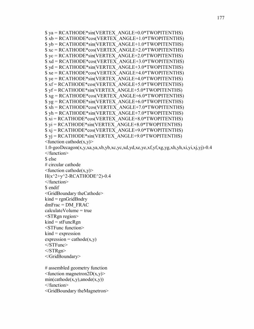
177
$ ya = RCATHODE*sin(VERTEX_ANGLE+0.0*TWOPITENTHS)
$ xb = RCATHODE*cos(VERTEX_ANGLE+1.0*TWOPITENTHS)
$ yb = RCATHODE*sin(VERTEX_ANGLE+1.0*TWOPITENTHS)
$ xc = RCATHODE*cos(VERTEX_ANGLE+2.0*TWOPITENTHS)
$ yc = RCATHODE*sin(VERTEX_ANGLE+2.0*TWOPITENTHS)
$ xd = RCATHODE*cos(VERTEX_ANGLE+3.0*TWOPITENTHS)
$ yd = RCATHODE*sin(VERTEX_ANGLE+3.0*TWOPITENTHS)
$ xe = RCATHODE*cos(VERTEX_ANGLE+4.0*TWOPITENTHS)
$ ye = RCATHODE*sin(VERTEX_ANGLE+4.0*TWOPITENTHS)
$ xf = RCATHODE*cos(VERTEX_ANGLE+5.0*TWOPITENTHS)
$ yf = RCATHODE*sin(VERTEX_ANGLE+5.0*TWOPITENTHS)
$ xg = RCATHODE*cos(VERTEX_ANGLE+6.0*TWOPITENTHS)
$ yg = RCATHODE*sin(VERTEX_ANGLE+6.0*TWOPITENTHS)
$ xh = RCATHODE*cos(VERTEX_ANGLE+7.0*TWOPITENTHS)
$ yh = RCATHODE*sin(VERTEX_ANGLE+7.0*TWOPITENTHS)
$ xi = RCATHODE*cos(VERTEX_ANGLE+8.0*TWOPITENTHS)
$ yi = RCATHODE*sin(VERTEX_ANGLE+8.0*TWOPITENTHS)
$ xj = RCATHODE*cos(VERTEX_ANGLE+9.0*TWOPITENTHS)
$ yj = RCATHODE*sin(VERTEX_ANGLE+9.0*TWOPITENTHS)
<function cathode(x,y)>
1.0-geoDecagon(x,y,xa,ya,xb,yb,xc,yc,xd,yd,xe,ye,xf,yf,xg,yg,xh,yh,xi,yi,xj,yj)-0.4
</function>
$ else
# circular cathode
<function cathode(x,y)>
H(x^2+y^2-RCATHODE^2)-0.4
</function>
$ endif
<GridBoundary theCathode>
kind = rgnGridBndry
dmFrac = DM_FRAC
calculateVolume = true
<STRgn region>
kind = stFuncRgn
<STFunc function>
kind = expression
expression = cathode(x,y)
</STFunc>
</STRgn>
</GridBoundary>
# assembled geometry function
<function magnetron2D(x,y)>
min(cathode(x,y),anode(x,y))
</function>
<GridBoundary theMagnetron>

178
kind = funcGridBndry
dmFrac = DM_FRAC
calculateVolume = true
<STFunc function>
kind = expression
expression = magnetron2D(x,y)
</STFunc>
</GridBoundary>
# cavity loading parameters
# ... only the first CAVITY1 along the positive X axis is loaded
$ RBGN_LOADING = 0.5*(RANODE+RCAVITY1)
$ LY_LOADING = RCAVITY1*ANGLECAVITY1+2.0*DY
$ IXBGN_LOADING = int((RBGN_LOADING-XBGN)/DX+0.5)
$ IYBGN_LOADING = int((-0.5*LY_LOADING -YBGN)/DY)
$ IYEND_LOADING = int(( 0.5*LY_LOADING -YBGN)/DY)+1
$ LOADING_FACTOR = sqrt((1.0-
0.5*DT*NU_LOADING)/(1.0+0.5*DT*NU_LOADING))
dimension = 2
floattype = double
<Grid globalGrid>
numPhysCells = [NX NY NZ]
lengths = [LX LY LZ]
startPositions = [XBGN YBGN ZSTART]
</Grid>
dt = DT
dumpPeriodicity = NSTEPSPERDUMP
nsteps = TIMESTEPS
<Decomp decomp>
decompType = regular
periodicDirs = [2]
</Decomp>
$ if INCLUDE_DC_VOLTAGE==1
# Generate electrostatic field between cathode and anode
# using combined source with feedback & drain
# and finite-difference divergence-free 1/r current profile
# normalized to charge equivalent cylindrical capacitior in RISETIME
$ APPROX_CAPACITANCE = TWOPI*EPSILON0/log(RANODE/RCATHODE)
$ CURRENT_DC = APPROX_CAPACITANCE*(VOLTAGE_DC/RISETIME)
<function rHatOverRcomponent1(x1,x2,DX1,DX2)>
(atan2(x1,x2-0.5*DX2)-atan2(x1,x2+0.5*DX2))/DX2
</function>
<function rHatOverRcomponent2(x1,x2,DX1,DX2)>
(atan2(x2,x1-0.5*DX1)-atan2(x2,x1+0.5*DX1))/DX1
</function>
<function rampup(t)>
1.0-exp(-1.0*max(0.0,t)/RISETIME)

179
</function>
<SumRhoJ sumRhoJ>
<Source feedbackVoltageSource>
kind = varadd
lowerBounds = [0 0 0]
upperBounds = [NX NY NZ]
components = [1 2]
<STFunc component1>
kind = feedbackSTFunc
feedback = voltageFeedback
expression = (CURRENT_DC/TWOPI)*rHatOverRcomponent1(x,y,DX,DY)
</STFunc>
<STFunc component2>
kind = feedbackSTFunc
feedback = voltageFeedback
expression = (CURRENT_DC/TWOPI)*rHatOverRcomponent2(x,y,DX,DY)
</STFunc>
</Source>
<Source constantVoltageDrain>
kind = varadd
lowerBounds = [0 0 0]
upperBounds = [NX NY NZ]
components = [1 2]
<STFunc component1>
kind = expression
expression = -
1.0*rampup(t)*(CURRENT_DC/TWOPI)*rHatOverRcomponent1(x,y,DX,DY)
</STFunc>
<STFunc component2>
kind = expression
expression = -
1.0*rampup(t)*(CURRENT_DC/TWOPI)*rHatOverRcomponent2(x,y,DX,DY)
</STFunc>
</Source>
</SumRhoJ>
$ endif
# the static magnetic field
<EmField myExternalBField>
kind = funcEmField
<Component Bz>
index = 5
<STFunc component5>
kind = expression
expression = BSTATIC
</STFunc>
</Component>

180
</EmField>
# the Maxwell Equations dynamic fields
<EmField YeeEmField>
kind = emMultiField
# - - - - - - - - - - - - - - - -
<Field edgeE>
numComponents = 3
offset = edge
</Field>
<Field faceB>
numComponents = 3
offset = face
</Field>
<Field nodalE>
numComponents = 3
overlap = [1 2]
offset = none
dumpPeriod = 0
</Field>
<Field nodalB>
numComponents = 3
overlap = [1 2]
offset = none
dumpPeriod = 0
</Field>
externalFields = [SumRhoJ]
# - - - - - - - - - - - - - - - -
<FieldMultiUpdater ampere>
gridBoundary = theMagnetron
interiorness = deymittra
kind = yeeAmpereUpdater
components = [0 1 2]
contractFromBottomInNonComponentDir = 1
lowerBounds = [0 0 0]
upperBounds = [NX NY NZ]
readFields = [faceB SumRhoJ]
writeFields = [edgeE]
</FieldMultiUpdater>
<FieldMultiUpdater faraday>
gridBoundary = theMagnetron
interiorness = deymittra
kind = yeeFaradayUpdater
components = [0 1 2]
expandToTopInComponentDir=1
lowerBounds = [0 0 0]
upperBounds = [NX NY NZ]

181
readFields = [edgeE]
writeFields = [faceB]
</FieldMultiUpdater>
<FieldUpdater deyMittraFaraday>
gridBoundary = theMagnetron
interiorness = deymittra
kind = deyMittraUpdater
lowerBounds = [0 0 0]
upperBounds = [NX NY NZ]
readFields = [edgeE]
writeFields = [faceB]
</FieldUpdater>
<FieldUpdater loadB>
kind = STFuncUpdater
operation = multiply
lowerBounds = [IXBGN_LOADING IYBGN_LOADING 0 ]
upperBounds = [$NX+1$ $IYEND_LOADING+1$ $NZ+1$]
component = 2
writeComponents = [2]
writeFields = [faceB]
<STFunc loadingFunction>
kind = expression
expression = LOADING_FACTOR
</STFunc>
</FieldUpdater>
<FieldUpdater computeNodalB>
kind = faceToNodeVec
lowerBounds = [0 0 0]
upperBounds = [NX NY NZ]
readFields = [faceB]
writeFields = [nodalB]
</FieldUpdater>
<FieldUpdater computeNodalE>
kind = edgeToNodeVec
lowerBounds = [0 0 0]
upperBounds = [NX NY NZ]
readFields = [edgeE]
writeFields = [nodalE]
</FieldUpdater>
$ if IMPULSE_EXCITATION==1
# want cavity1Voltage to be roughly 0.1*VOLTAGE_DC
$ BNORMALIZATION =
(0.1*VOLTAGE_DC/(ANGLECAVITY1*RANODE)/LIGHTSPEED)*(0.05*DT/DT)
<function excitationPulse(t)>
BNORMALIZATION*sin(PI*max(0.0,min(1.0,0.05*t/DT)))^2
</function>

182
<function singleCavityProfile(x,y,z)>
H(x^2+y^2-RANODE^2)*H(cavities1(x,y))*H(0.5*PI/NCAVITY-
abs(atan2(y,x)))*cos(0.5*PI*(RCAVITY1-sqrt(x^2+y^2))/(RCAVITY1-RANODE))^2
</function>
<FieldUpdater impluseBz>
kind = STFuncUpdater
operation = add
lowerBounds = [0 0 0]
upperBounds = [NX NY NZ]
component = 2
writeComponents = [2]
writeFields = [faceB]
<STFunc loadingFunction>
kind = expression
expression = excitationPulse(t)*singleCavityProfile(x,y,z)
</STFunc>
</FieldUpdater>
$ endif
$ if PI_MODE_PRIMING==1
# want cavity1Voltage to be roughly 0.1*VOLTAGE_DC
$ BNORMALIZATION =
(0.1*VOLTAGE_DC/(ANGLECAVITY1*RANODE)/LIGHTSPEED)*(4.0*DT/RISETI
ME)
<function primePulse(t)>
BNORMALIZATION*sin(PI*max(0.0,min(1.0,4.0*t/RISETIME)))^2
</function>
# The approximate BzProfile should try to have the null lines roughly in the correct
location
# ... Rising Sun Mode has node partway up the long cavity arm, had to work hard for
that!
$ RNULL = RANODE*(1.0-0.5*PI/NCAVITY) + 0.5*abs(RCAVITY1-RCAVITY2)
$ KCAVITY = 0.5*PI/(max(RCAVITY1,RCAVITY2)-RNULL)
$ FCAV1 = cos(KCAVITY*(RCAVITY1-RANODE))
$ FCAV2 = -1.0*cos(KCAVITY*(RCAVITY2-RANODE))
$ FCAVA = 0.5*(FCAV1+FCAV2)
$ FCAVD = 0.5*(FCAV1-FCAV2)
<function approximateBzProfile(x,y,z)>
H(x^2+y^2-
RANODE^2)*H(cavities1(x,y))*abs(cos(NCAVITY*atan2(y,x)))*cos(KCAVITY*(RCA
VITY1-sqrt(x^2+y^2))) - \
H(x^2+y^2-
RANODE^2)*H(cavities2(x,y))*abs(cos(NCAVITY*atan2(y,x)))*cos(KCAVITY*(RCA
VITY2-sqrt(x^2+y^2))) + \
H(RANODE^2-x^2-y^2)*H(cathode(x,y))
*abs(cos(NCAVITY*atan2(y,x)))*FCAVD*((sqrt(x^2+y^2)-RCATHODE)/(RANODE-
RCATHODE))^2*(-1.0+2.0*H(cos(NCAVITY*atan2(y,x)))) + \

183
H(RANODE^2-x^2-y^2)*H(cathode(x,y))*FCAVA
</function>
<FieldUpdater primeBz>
kind = STFuncUpdater
operation = add
lowerBounds = [0 0 0]
upperBounds = [NX NY NZ]
component = 2
writeComponents = [2]
writeFields = [faceB]
<STFunc loadingFunction>
kind = expression
expression = primePulse(t)*approximateBzProfile(x,y,z)
</STFunc>
</FieldUpdater>
$ endif
# - - - - - - - - - - - - - - - -
<InitialUpdateStep init_step1>
alsoAfterRestore = 1
toDtFrac = 0.
updaters = [computeNodalE]
messageFields = [nodalE]
</InitialUpdateStep>
<InitialUpdateStep init_step2>
alsoAfterRestore = 1
toDtFrac = 0.
messageFields = [nodalB]
updaters = [computeNodalB]
</InitialUpdateStep>
<UpdateStep step1>
toDtFrac = 0.5
updaters = [loadB faraday deyMittraFaraday]
messageFields = [faceB]
</UpdateStep>
<UpdateStep step2>
toDtFrac = 1.0
updaters = [ampere]
messageFields = [edgeE]
</UpdateStep>
<UpdateStep step3>
toDtFrac = 1.0
$ if (IMPULSE_EXCITATION==1) and (PI_MODE_PRIMING==1)
updaters = [faraday deyMittraFaraday loadB impluseBz primeBz]
$ endif
$ if (IMPULSE_EXCITATION==1) and (PI_MODE_PRIMING==0)
updaters = [faraday deyMittraFaraday loadB impluseBz]

184
$ endif
$ if (IMPULSE_EXCITATION==0) and (PI_MODE_PRIMING==1)
updaters = [faraday deyMittraFaraday loadB primeBz]
$ endif
$ if (IMPULSE_EXCITATION==0) and (PI_MODE_PRIMING==0)
updaters = [faraday deyMittraFaraday loadB]
$ endif
messageFields = [faceB]
</UpdateStep>
<UpdateStep step4>
toDtFrac = 1.
updaters = [computeNodalE]
messageFields = [nodalE]
</UpdateStep>
<UpdateStep step5>
toDtFrac = 1.
updaters = [computeNodalB]
messageFields = [nodalB]
</UpdateStep>
# - - - - - - - - - - - - - - - -
</EmField>
# diagnostics
$ IX_AXIS = int((0.0-XBGN)/DX+0.5)
$ IY_AXIS = int((0.0-YBGN)/DY+0.5)
<History cathodeAnodeVoltage>
kind = pseudoPotential
field = YeeEmField.edgeE
referencePoint = [IX_AXIS IY_AXIS]
measurePoint = [NX IY_AXIS]
</History>
$ RBGN_LOADING = 0.5*(RANODE+RCAVITY1)
$ IX_CAVITY1_LINE = int((RANODE -XBGN)/DX)+2
$ IX_CAVITY1_POINT = int((RCAVITY1-XBGN)/DX)-1
$ LY_CAVITY_LINE = RANODE*ANGLECAVITY1+2.0*DY
$ IYBGN_CAVITY_LINE = int((-0.5*LY_CAVITY_LINE-YBGN)/DY)
$ IYEND_CAVITY_LINE = int(( 0.5*LY_CAVITY_LINE-YBGN)/DY)+1
<History cavity1Voltage>
kind = pseudoPotential
field = YeeEmField.edgeE
referencePoint = [IX_CAVITY1_LINE IYBGN_CAVITY_LINE]
measurePoint = [IX_CAVITY1_LINE IYEND_CAVITY_LINE]
</History>
<History cavity1Bfield_Tesla>
kind = fieldAtIndices
point = [IX_CAVITY1_POINT IY_AXIS]
field = YeeEmField.faceB

185
components = [2]
</History>
<History cavity1Loading_Watts>
kind = fieldPoyn
lowerBounds = [$IXBGN_LOADING-1$ IYBGN_LOADING 0 ]
upperBounds = [$IXBGN_LOADING-1$ $IYEND_LOADING+1$ $NZ+1$]
fields = [YeeEmField.edgeE YeeEmField.faceB]
</History>
<History fieldEnergy_Joules>
kind = EMfieldEnergy
fields = [YeeEmField.edgeE YeeEmField.faceB]
</History>
# special diagnostic for DC voltage feedback
$ if INCLUDE_DC_VOLTAGE==1
<History voltageFeedback>
kind=feedback
feedbackHist=cathodeAnodeVoltage
timeConstant=RISETIME
<STFunc desiredHistory>
kind=expression
expression = VOLTAGE_DC*rampup(t)
</STFunc>
</History>
$ endif
$ if INCLUDE_PARTICLES == 1
# the fields used for the Lorentz force
<ComboEmField myComboEmField>
kind = comboEmField
emField1 = YeeEmField
emField2 = myExternalBField
dumpField = 0
</ComboEmField>
# emission algorithm parameters
$ PARTPERCELLPERSTEP = 10
$ AREA_EMIT = 2.0*PI*RCATHODE
$ APPROXNUMEMITCELLS = AREA_EMIT/sqrt(DY*DX)
$ JDENS_EMIT = EMITTED_CURRENT/AREA_EMIT
$ NOM_DEN =
EMITTED_CURRENT*DT/(ELEMCHARGE*APPROXNUMEMITCELLS*PARTPE
RCELLPERSTEP)
$ FOREVER = 1.0*SECONDS
$ VTHERMAL = 1.5e5 # meters/second
<Species electrons>
verbosity = 0
kind=relBorisVW
charge = ELECCHARGE

186
mass = ELECMASS
emField = myComboEmField
nominalDensity = NOM_DEN
nomPtclsPerCell = PARTPERCELLPERSTEP
numPtclsInMacro = 1.0e5
<ParticleSource cutCellEmitter>
kind = xvLoaderEmitter
positionFunction = random
useCornerMove = true
emitBasedOnLocalForce = true
loadOnShift = false
loadAfterInit = false
applyTimes = [RISETIME FOREVER]
<PositionGenerator thisGen>
kind = cutCellPosGen
numMacroPtclsPerStep = PARTPERCELLPERSTEP
emitterBoundary = theCathode
emissionOffset = 0.1
</PositionGenerator>
<VelocityGenerator emitVelGen>
kind = funcVelGen
velocityIsLocal = true
<STFunc component0>
kind = expression
expression = -1.0*VTHERMAL
</STFunc>
</VelocityGenerator>
<STFunc currentDensityFunc>
kind = expression
expression = JDENS_EMIT
</STFunc>
</ParticleSource>
<ParticleSink cathodeElectronSink>
kind = absSavCutCell
gridBoundary = theCathode
lowerBounds = [ -1 -1 -1 ]
upperBounds = [$NX+1$ $NY+1$ $NZ+1$]
</ParticleSink>
<ParticleSink anodeElectronSink>
kind = absSavCutCell
gridBoundary = theAnode
lowerBounds = [ -1 -1 -1 ]
upperBounds = [$NX+1$ $NY+1$ $NZ+1$]
</ParticleSink>
</Species>
<History anodeCurrent_Amps>

187
kind = speciesCurrAbs
species = electrons
ptclAbsorber = anodeElectronSink
</History>
<History cathodeReturnCurrent_Amps>
kind = speciesCurrAbs
species = electrons
ptclAbsorber = cathodeElectronSink
</History>
<History anodeElectronHeat_Watts_timesDT>
kind = speciesEngyAbs
species = electrons
ptclAbsorber = anodeElectronSink
</History>
<History cathodeElectronHeat_Watts_timesDT>
kind = speciesEngyAbs
species = electrons
ptclAbsorber = cathodeElectronSink
</History>
<History numMacroParticles>
kind = speciesNumberOf
species = electrons
</History>
$ endif

188
Modulated, Addressable Cathode
##Current density model changes from previous code.
# emission algorithm parameters
$ MASK_FACTOR = min(NUMBER_OF_EMITTERS*(PHIEND_EMIT-
PHIBGN_EMIT)/TWOPI,1.0)
$ PARTPERCELLPERSTEP = int(3.0/MASK_FACTOR+0.5)
$ AREA_EMIT = 2.0*PI*RCATHODE*MASK_FACTOR
$ APPROXNUMEMITCELLS = AREA_EMIT/sqrt(DY*DX)
$ JDENS_EMIT = EMITTED_CURRENT/AREA_EMIT
$ NOM_DEN =
EMITTED_CURRENT*DT/(ELEMCHARGE*APPROXNUMEMITCELLS*PARTPE
RCELLPERSTEP)
$ FOREVER = 1.0*SECONDS
$ VTHERMAL = 1.5e5 # meters/second
$ DPHI_EMIT = TWOPI/NUMBER_OF_EMITTERS
<function emissionAngle(x,y)>
mod(atan2(y,x)+TWOPI+0.5*DPHI_EMIT,DPHI_EMIT)-0.5*DPHI_EMIT
</function>
<function emissionMask(x,y)>
H(PHIEND_EMIT-emissionAngle(x,y))*H(emissionAngle(x,y)-PHIBGN_EMIT)
</function>
<Species electrons>
verbosity = 0
kind=relBorisVW
charge = ELECCHARGE
mass = ELECMASS
emField = myComboEmField
nominalDensity = NOM_DEN
nomPtclsPerCell = PARTPERCELLPERSTEP
numPtclsInMacro = 1.0e5
#Macro for particle source (multiple emitters)
<macro ParticleSourceat(source_name,phibgn,phiend,tbegin,tend)>
<ParticleSource source_name>
kind = xvLoaderEmitter
positionFunction = random
useCornerMove = true
emitBasedOnLocalForce = true
loadOnShift = false
loadAfterInit = false
applyTimes = [tbegin tend]
<PositionGenerator thisGen>
kind = cutCellPosGen

189
numMacroPtclsPerStep = PARTPERCELLPERSTEP
emitterBoundary = theCathode
emissionOffset = 0.1
<STFunc mask>
kind = expression
expression = H((phiend)-atan2(y,x))*H(atan2(y,x)-(phibgn))
</STFunc>
</PositionGenerator>
<VelocityGenerator emitVelGen>
kind = funcVelGen
velocityIsLocal = true
<STFunc component0>
kind = expression
expression = -1.0*VTHERMAL
</STFunc>
</VelocityGenerator>
<STFunc currentDensityFunc>
kind = expression
expression = JDENS_EMIT*emissionMask(x,y)
</STFunc>
</ParticleSource>
</macro>
<function fix_angle(angle)>
mod(angle+PI,TWOPI)-PI
</function>
###Location of each current source. This corresponds to the ten-sided cathode.
###PHIBGN – start location of the current source.
###PHIEND – end location of the current source.
########################################################################
########################1/5
$PHIBGN1=fix_angle(VERTEX_ANGLE+0.1699*TWOPITENTHS+0.1699*TWOPIT
ENTHS/NUMBER_OF_EMITTERS)-5.0*DEGREES
$PHIEND1=fix_angle(VERTEX_ANGLE+0.1699*TWOPITENTHS+0.1699*TWOPIT
ENTHS/NUMBER_OF_EMITTERS)+5.0*DEGREES
$PHIBGN2=fix_angle(VERTEX_ANGLE+0.40*TWOPITENTHS+0.40*TWOPITENT
HS/NUMBER_OF_EMITTERS)-5.0*DEGREES
$PHIEND2=fix_angle(VERTEX_ANGLE+0.40*TWOPITENTHS+0.40*TWOPITENT
HS/NUMBER_OF_EMITTERS)+5.0*DEGREES
$PHIBGN3=fix_angle(VERTEX_ANGLE+0.65*TWOPITENTHS+0.65*TWOPITENT
HS/NUMBER_OF_EMITTERS)-5.0*DEGREES
$PHIEND3=fix_angle(VERTEX_ANGLE+0.65*TWOPITENTHS+0.65*TWOPITENT
HS/NUMBER_OF_EMITTERS)+5.0*DEGREES
$PHIBGN4=fix_angle(VERTEX_ANGLE+0.99*TWOPITENTHS+0.99*TWOPITENT
HS/NUMBER_OF_EMITTERS)-5.0*DEGREES

190
$PHIEND4=fix_angle(VERTEX_ANGLE+0.99*TWOPITENTHS+0.99*TWOPITENT
HS/NUMBER_OF_EMITTERS)+5.0*DEGREES
$PHIBGN5=fix_angle(VERTEX_ANGLE+1.26*TWOPITENTHS+1.26*TWOPITENT
HS/NUMBER_OF_EMITTERS)-5.0*DEGREES
$PHIEND5=fix_angle(VERTEX_ANGLE+1.26*TWOPITENTHS+1.26*TWOPITENT
HS/NUMBER_OF_EMITTERS)+5.0*DEGREES
$PHIBGN6=fix_angle(VERTEX_ANGLE+1.54*TWOPITENTHS+1.54*TWOPITENT
HS/NUMBER_OF_EMITTERS)-5.0*DEGREES
$PHIEND6=fix_angle(VERTEX_ANGLE+1.54*TWOPITENTHS+1.54*TWOPITENT
HS/NUMBER_OF_EMITTERS)+5.0*DEGREES
$PHIBGN7=fix_angle(VERTEX_ANGLE+1.80*TWOPITENTHS+1.80*TWOPITENT
HS/NUMBER_OF_EMITTERS)-5.0*DEGREES
$PHIEND7=fix_angle(VERTEX_ANGLE+1.80*TWOPITENTHS+1.80*TWOPITENT
HS/NUMBER_OF_EMITTERS)+5.0*DEGREES
$PHIBGN8=fix_angle(VERTEX_ANGLE+2.09*TWOPITENTHS+2.09*TWOPITENT
HS/NUMBER_OF_EMITTERS)-5.0*DEGREES
$PHIEND8=fix_angle(VERTEX_ANGLE+2.09*TWOPITENTHS+2.09*TWOPITENT
HS/NUMBER_OF_EMITTERS)+5.0*DEGREES
$PHIBGN9=fix_angle(VERTEX_ANGLE+2.36*TWOPITENTHS+2.36*TWOPITENT
HS/NUMBER_OF_EMITTERS)-5.0*DEGREES
$PHIEND9=fix_angle(VERTEX_ANGLE+2.36*TWOPITENTHS+2.36*TWOPITENT
HS/NUMBER_OF_EMITTERS)+5.0*DEGREES
$PHIBGN10=fix_angle(VERTEX_ANGLE+2.65*TWOPITENTHS+2.65*TWOPITEN
THS/NUMBER_OF_EMITTERS)-5.0*DEGREES
$PHIEND10=fix_angle(VERTEX_ANGLE+2.65*TWOPITENTHS+2.65*TWOPITEN
THS/NUMBER_OF_EMITTERS)+5.0*DEGREES
$PHIBGN11=fix_angle(VERTEX_ANGLE+2.92*TWOPITENTHS+2.92*TWOPITEN
THS/NUMBER_OF_EMITTERS)-5.0*DEGREES
$PHIEND11=fix_angle(VERTEX_ANGLE+2.92*TWOPITENTHS+2.92*TWOPITEN
THS/NUMBER_OF_EMITTERS)+5.0*DEGREES
$PHIBGN12=fix_angle(VERTEX_ANGLE+3.20*TWOPITENTHS+3.20*TWOPITEN
THS/NUMBER_OF_EMITTERS)-5.0*DEGREES
$PHIEND12=fix_angle(VERTEX_ANGLE+3.20*TWOPITENTHS+3.20*TWOPITEN
THS/NUMBER_OF_EMITTERS)+5.0*DEGREES
$PHIBGN13=fix_angle(VERTEX_ANGLE+3.50*TWOPITENTHS+3.50*TWOPITEN
THS/NUMBER_OF_EMITTERS)-5.0*DEGREES
$PHIEND13=fix_angle(VERTEX_ANGLE+3.50*TWOPITENTHS+3.50*TWOPITEN
THS/NUMBER_OF_EMITTERS)+5.0*DEGREES
$PHIBGN14=fix_angle(VERTEX_ANGLE+3.75*TWOPITENTHS+3.75*TWOPITEN
THS/NUMBER_OF_EMITTERS)-5.0*DEGREES
$PHIEND14=fix_angle(VERTEX_ANGLE+3.75*TWOPITENTHS+3.75*TWOPITEN
THS/NUMBER_OF_EMITTERS)+5.0*DEGREES
$PHIBGN15=fix_angle(VERTEX_ANGLE+4.00*TWOPITENTHS+4.00*TWOPITEN
THS/NUMBER_OF_EMITTERS)-5.0*DEGREES
$PHIEND15=fix_angle(VERTEX_ANGLE+4.00*TWOPITENTHS+4.00*TWOPITEN
THS/NUMBER_OF_EMITTERS)+5.0*DEGREES

191
$PHIBGN16=fix_angle(VERTEX_ANGLE+4.30*TWOPITENTHS+4.30*TWOPITEN
THS/NUMBER_OF_EMITTERS)-5.0*DEGREES
$PHIEND16=fix_angle(VERTEX_ANGLE+4.30*TWOPITENTHS+4.30*TWOPITEN
THS/NUMBER_OF_EMITTERS)+5.0*DEGREES
$PHIBGN17=fix_angle(VERTEX_ANGLE+4.60*TWOPITENTHS+4.55*TWOPITEN
THS/NUMBER_OF_EMITTERS)-5.0*DEGREES
$PHIEND17=fix_angle(VERTEX_ANGLE+4.60*TWOPITENTHS+4.55*TWOPITEN
THS/NUMBER_OF_EMITTERS)+5.0*DEGREES
$PHIBGN18=fix_angle(VERTEX_ANGLE+4.85*TWOPITENTHS+4.85*TWOPITEN
THS/NUMBER_OF_EMITTERS)-5.0*DEGREES
$PHIEND18=fix_angle(VERTEX_ANGLE+4.85*TWOPITENTHS+4.85*TWOPITEN
THS/NUMBER_OF_EMITTERS)+5.0*DEGREES
$PHIBGN19=fix_angle(VERTEX_ANGLE+5.15*TWOPITENTHS+5.15*TWOPITEN
THS/NUMBER_OF_EMITTERS)-5.0*DEGREES
$PHIEND19=fix_angle(VERTEX_ANGLE+5.15*TWOPITENTHS+5.15*TWOPITEN
THS/NUMBER_OF_EMITTERS)+5.0*DEGREES
$PHIBGN20=fix_angle(VERTEX_ANGLE+5.43*TWOPITENTHS+5.43*TWOPITEN
THS/NUMBER_OF_EMITTERS)-5.0*DEGREES
$PHIEND20=fix_angle(VERTEX_ANGLE+5.43*TWOPITENTHS+5.43*TWOPITEN
THS/NUMBER_OF_EMITTERS)+5.0*DEGREES
$PHIBGN21=fix_angle(VERTEX_ANGLE+5.71*TWOPITENTHS+5.71*TWOPITEN
THS/NUMBER_OF_EMITTERS)-5.0*DEGREES
$PHIEND21=fix_angle(VERTEX_ANGLE+5.71*TWOPITENTHS+5.71*TWOPITEN
THS/NUMBER_OF_EMITTERS)+5.0*DEGREES
$PHIBGN22=fix_angle(VERTEX_ANGLE+5.98*TWOPITENTHS+5.98*TWOPITEN
THS/NUMBER_OF_EMITTERS)-6.5*DEGREES
$PHIEND22=fix_angle(VERTEX_ANGLE+5.98*TWOPITENTHS+5.98*TWOPITEN
THS/NUMBER_OF_EMITTERS)+6.5*DEGREES
$PHIBGN23=fix_angle(VERTEX_ANGLE+6.3*TWOPITENTHS+6.28*TWOPITENT
HS/NUMBER_OF_EMITTERS)-5.7*DEGREES
$PHIEND23=fix_angle(VERTEX_ANGLE+6.3*TWOPITENTHS+6.28*TWOPITENT
HS/NUMBER_OF_EMITTERS)+5.7*DEGREES
$PHIBGN31=fix_angle(VERTEX_ANGLE+6.3*TWOPITENTHS+6.28*TWOPITENT
HS/NUMBER_OF_EMITTERS)-5.7*DEGREES+TWOPI
$PHIEND31=fix_angle(VERTEX_ANGLE+6.3*TWOPITENTHS+6.28*TWOPITENT
HS/NUMBER_OF_EMITTERS)+5.7*DEGREES+TWOPI
$PHIBGN24=fix_angle(VERTEX_ANGLE+6.50*TWOPITENTHS+6.50*TWOPITEN
THS/NUMBER_OF_EMITTERS)-5.0*DEGREES
$PHIEND24=fix_angle(VERTEX_ANGLE+6.50*TWOPITENTHS+6.50*TWOPITEN
THS/NUMBER_OF_EMITTERS)+5.0*DEGREES
$PHIBGN25=fix_angle(VERTEX_ANGLE+6.80*TWOPITENTHS+6.80*TWOPITEN
THS/NUMBER_OF_EMITTERS)-5.0*DEGREES
$PHIEND25=fix_angle(VERTEX_ANGLE+6.80*TWOPITENTHS+6.80*TWOPITEN
THS/NUMBER_OF_EMITTERS)+5.0*DEGREES
$PHIBGN26=fix_angle(VERTEX_ANGLE+7.09*TWOPITENTHS+7.09*TWOPITEN
THS/NUMBER_OF_EMITTERS)-5.0*DEGREES

192
$PHIEND26=fix_angle(VERTEX_ANGLE+7.09*TWOPITENTHS+7.09*TWOPITEN
THS/NUMBER_OF_EMITTERS)+5.0*DEGREES
$PHIBGN27=fix_angle(VERTEX_ANGLE+7.35*TWOPITENTHS+7.35*TWOPITEN
THS/NUMBER_OF_EMITTERS)-5.0*DEGREES
$PHIEND27=fix_angle(VERTEX_ANGLE+7.35*TWOPITENTHS+7.35*TWOPITEN
THS/NUMBER_OF_EMITTERS)+5.0*DEGREES
$PHIBGN28=fix_angle(VERTEX_ANGLE+7.65*TWOPITENTHS+7.65*TWOPITEN
THS/NUMBER_OF_EMITTERS)-5.0*DEGREES
$PHIEND28=fix_angle(VERTEX_ANGLE+7.65*TWOPITENTHS+7.65*TWOPITEN
THS/NUMBER_OF_EMITTERS)+5.0*DEGREES
$PHIBGN29=fix_angle(VERTEX_ANGLE+7.92*TWOPITENTHS+7.92*TWOPITEN
THS/NUMBER_OF_EMITTERS)-5.0*DEGREES
$PHIEND29=fix_angle(VERTEX_ANGLE+7.92*TWOPITENTHS+7.92*TWOPITEN
THS/NUMBER_OF_EMITTERS)+5.0*DEGREES
$PHIBGN30=fix_angle(VERTEX_ANGLE+8.20*TWOPITENTHS+8.20*TWOPITEN
THS/NUMBER_OF_EMITTERS)-5.0*DEGREES
$PHIEND30=fix_angle(VERTEX_ANGLE+8.20*TWOPITENTHS+8.20*TWOPITEN
THS/NUMBER_OF_EMITTERS)+5.0*DEGREES
########################################################################
###########################
##########This portion of the code show 5 periods of the modulated current sources
###1/5
###########################################################1/5
ParticleSourceat(mysource1,PHIBGN1,PHIEND1,0.00e-10,1.73e-10)
ParticleSourceat(mysource2,PHIBGN2,PHIEND2,1.73e-10,3.47e-10)
ParticleSourceat(mysource3,PHIBGN3,PHIEND3,3.47e-10,5.20e-10)
ParticleSourceat(mysource4,PHIBGN4,PHIEND4,5.20e-10,6.93e-10)
ParticleSourceat(mysource5,PHIBGN5,PHIEND5,6.93e-10,8.67e-10)
ParticleSourceat(mysource6,PHIBGN6,PHIEND6,8.67e-10,1.04e-09)
ParticleSourceat(mysource7,PHIBGN7,PHIEND7,0.00e-10,1.73e-10)
ParticleSourceat(mysource8,PHIBGN8,PHIEND8,1.73e-10,3.47e-10)
ParticleSourceat(mysource9,PHIBGN9,PHIEND9,3.47e-10,5.20e-10)
ParticleSourceat(mysource10,PHIBGN10,PHIEND10,5.20e-10,6.93e-10)
ParticleSourceat(mysource11,PHIBGN11,PHIEND11,6.93e-10,8.67e-10)
ParticleSourceat(mysource12,PHIBGN12,PHIEND12,8.67e-10,1.04e-09)
ParticleSourceat(mysource13,PHIBGN13,PHIEND13,0.00e-10,1.73e-10)
ParticleSourceat(mysource14,PHIBGN14,PHIEND14,1.73e-10,3.47e-10)
ParticleSourceat(mysource15,PHIBGN15,PHIEND15,3.47e-10,5.20e-10)
ParticleSourceat(mysource16,PHIBGN16,PHIEND16,5.20e-10,6.93e-10)
ParticleSourceat(mysource17,PHIBGN17,PHIEND17,6.93e-10,8.67e-10)
ParticleSourceat(mysource18,PHIBGN18,PHIEND18,8.67e-10,1.04e-09)
ParticleSourceat(mysource19,PHIBGN19,PHIEND19,0.00e-10,1.73e-10)
ParticleSourceat(mysource20,PHIBGN20,PHIEND20,1.73e-10,3.47e-10)
ParticleSourceat(mysource21,PHIBGN21,PHIEND21,3.47e-10,5.20e-10)
ParticleSourceat(mysource22,PHIBGN22,PHIEND22,5.20e-10,6.93e-10)
ParticleSourceat(mysource23,PHIBGN23,PHIEND23,6.93e-10,8.67e-10)

193
ParticleSourceat(mysource31,PHIBGN31,PHIEND31,6.93e-10,8.67e-10)
ParticleSourceat(mysource24,PHIBGN24,PHIEND24,8.67e-10,1.04e-09)
ParticleSourceat(mysource25,PHIBGN25,PHIEND25,0.00e-10,1.73e-10)
ParticleSourceat(mysource26,PHIBGN26,PHIEND26,1.73e-10,3.47e-10)
ParticleSourceat(mysource27,PHIBGN27,PHIEND27,3.47e-10,5.20e-10)
ParticleSourceat(mysource28,PHIBGN28,PHIEND28,5.20e-10,6.93e-10)
ParticleSourceat(mysource29,PHIBGN29,PHIEND29,6.93e-10,8.67e-10)
ParticleSourceat(mysource30,PHIBGN30,PHIEND30,8.67e-10,1.04e-09)
##################################################################
###2/5
###########################################################2/5
ParticleSourceat(mysource31,PHIBGN1,PHIEND1,1.04e-09,1.21e-09)
ParticleSourceat(mysource32,PHIBGN2,PHIEND2,1.21e-09,1.39e-09)
ParticleSourceat(mysource33,PHIBGN3,PHIEND3,1.39e-09,1.56e-09)
ParticleSourceat(mysource34,PHIBGN4,PHIEND4,1.56e-09,1.73e-09)
ParticleSourceat(mysource35,PHIBGN5,PHIEND5,1.73e-09,1.91e-09)
ParticleSourceat(mysource36,PHIBGN6,PHIEND6,1.91e-09,2.08e-09)
ParticleSourceat(mysource37,PHIBGN7,PHIEND7,1.04e-09,1.21e-09)
ParticleSourceat(mysource38,PHIBGN8,PHIEND8,1.21e-09,1.39e-09)
ParticleSourceat(mysource39,PHIBGN9,PHIEND9,1.39e-09,1.56e-09)
ParticleSourceat(mysource40,PHIBGN10,PHIEND10,1.56e-09,1.73e-09)
ParticleSourceat(mysource41,PHIBGN11,PHIEND11,1.73e-09,1.91e-09)
ParticleSourceat(mysource42,PHIBGN12,PHIEND12,1.91e-09,2.08e-09)
ParticleSourceat(mysource43,PHIBGN13,PHIEND13,1.04e-09,1.21e-09)
ParticleSourceat(mysource44,PHIBGN14,PHIEND14,1.21e-09,1.39e-09)
ParticleSourceat(mysource45,PHIBGN15,PHIEND15,1.39e-09,1.56e-09)
ParticleSourceat(mysource46,PHIBGN16,PHIEND16,1.56e-09,1.73e-09)
ParticleSourceat(mysource47,PHIBGN17,PHIEND17,1.73e-09,1.91e-09)
ParticleSourceat(mysource48,PHIBGN18,PHIEND18,1.91e-09,2.08e-09)
ParticleSourceat(mysource49,PHIBGN19,PHIEND19,1.04e-09,1.21e-09)
ParticleSourceat(mysource50,PHIBGN20,PHIEND20,1.21e-09,1.39e-09)
ParticleSourceat(mysource51,PHIBGN21,PHIEND21,1.39e-09,1.56e-09)
ParticleSourceat(mysource52,PHIBGN22,PHIEND22,1.56e-09,1.73e-09)
ParticleSourceat(mysource53,PHIBGN23,PHIEND23,1.73e-09,1.91e-09)
ParticleSourceat(mysource54,PHIBGN31,PHIEND31,1.73e-09,1.91e-09)
ParticleSourceat(mysource55,PHIBGN24,PHIEND24,1.91e-09,2.08e-09)
ParticleSourceat(mysource56,PHIBGN25,PHIEND25,1.04e-09,1.21e-09)
ParticleSourceat(mysource57,PHIBGN26,PHIEND26,1.21e-09,1.39e-09)
ParticleSourceat(mysource58,PHIBGN27,PHIEND27,1.39e-09,1.56e-09)
ParticleSourceat(mysource59,PHIBGN28,PHIEND28,1.56e-09,1.73e-09)
ParticleSourceat(mysource60,PHIBGN29,PHIEND29,1.73e-09,1.91e-09)
ParticleSourceat(mysource61,PHIBGN30,PHIEND30,1.91e-09,2.08e-09)
##################################################################
###3/5
###########################################################3/5
ParticleSourceat(mysource71,PHIBGN1,PHIEND1,2.08e-09,2.25e-09)

194
ParticleSourceat(mysource72,PHIBGN2,PHIEND2,2.25e-09,2.43e-09)
ParticleSourceat(mysource73,PHIBGN3,PHIEND3,2.43e-09,2.60e-09)
ParticleSourceat(mysource74,PHIBGN4,PHIEND4,2.60e-09,2.77e-09)
ParticleSourceat(mysource75,PHIBGN5,PHIEND5,2.77e-09,2.95e-09)
ParticleSourceat(mysource76,PHIBGN6,PHIEND6,2.95e-09,3.12e-09)
ParticleSourceat(mysource77,PHIBGN7,PHIEND7,2.08e-09,2.25e-09)
ParticleSourceat(mysource78,PHIBGN8,PHIEND8,2.25e-09,2.43e-09)
ParticleSourceat(mysource79,PHIBGN9,PHIEND9,2.43e-09,2.60e-09)
ParticleSourceat(mysource80,PHIBGN10,PHIEND10,2.60e-09,2.77e-09)
ParticleSourceat(mysource81,PHIBGN11,PHIEND11,2.77e-09,2.95e-09)
ParticleSourceat(mysource82,PHIBGN12,PHIEND12,2.95e-09,3.12e-09)
ParticleSourceat(mysource83,PHIBGN13,PHIEND13,2.08e-09,2.25e-09)
ParticleSourceat(mysource84,PHIBGN14,PHIEND14,2.25e-09,2.43e-09)
ParticleSourceat(mysource85,PHIBGN15,PHIEND15,2.43e-09,2.60e-09)
ParticleSourceat(mysource86,PHIBGN16,PHIEND16,2.60e-09,2.77e-09)
ParticleSourceat(mysource87,PHIBGN17,PHIEND17,2.77e-09,2.95e-09)
ParticleSourceat(mysource88,PHIBGN18,PHIEND18,2.95e-09,3.12e-09)
ParticleSourceat(mysource89,PHIBGN19,PHIEND19,2.08e-09,2.25e-09)
ParticleSourceat(mysource90,PHIBGN20,PHIEND20,2.25e-09,2.43e-09)
ParticleSourceat(mysource91,PHIBGN21,PHIEND21,2.43e-09,2.60e-09)
ParticleSourceat(mysource92,PHIBGN22,PHIEND22,2.60e-09,2.77e-09)
ParticleSourceat(mysource93,PHIBGN23,PHIEND23,2.77e-09,2.95e-09)
ParticleSourceat(mysource94,PHIBGN31,PHIEND31,2.77e-09,2.95e-09)
ParticleSourceat(mysource95,PHIBGN24,PHIEND24,2.95e-09,3.12e-09)
ParticleSourceat(mysource96,PHIBGN25,PHIEND25,2.08e-09,2.25e-09)
ParticleSourceat(mysource97,PHIBGN26,PHIEND26,2.25e-09,2.43e-09)
ParticleSourceat(mysource98,PHIBGN27,PHIEND27,2.43e-09,2.60e-09)
ParticleSourceat(mysource99,PHIBGN28,PHIEND28,2.60e-09,2.77e-09)
ParticleSourceat(mysource100,PHIBGN29,PHIEND29,2.77e-09,2.95e-09)
ParticleSourceat(mysource101,PHIBGN30,PHIEND30,2.95e-09,3.12e-09)
##################################################################
###4/5
###########################################################4/5
ParticleSourceat(mysource101,PHIBGN1,PHIEND1,3.12e-09,3.29e-09)
ParticleSourceat(mysource102,PHIBGN2,PHIEND2,3.29e-09,3.47e-09)
ParticleSourceat(mysource103,PHIBGN3,PHIEND3,3.47e-09,3.64e-09)
ParticleSourceat(mysource104,PHIBGN4,PHIEND4,3.64e-09,3.81e-09)
ParticleSourceat(mysource105,PHIBGN5,PHIEND5,3.81e-09,3.99e-09)
ParticleSourceat(mysource106,PHIBGN6,PHIEND6,3.99e-09,4.16e-09)
ParticleSourceat(mysource107,PHIBGN7,PHIEND7,3.12e-09,3.29e-09)
ParticleSourceat(mysource108,PHIBGN8,PHIEND8,3.29e-09,3.47e-09)
ParticleSourceat(mysource109,PHIBGN9,PHIEND9,3.47e-09,3.64e-09)
ParticleSourceat(mysource110,PHIBGN10,PHIEND10,3.64e-09,3.81e-09)
ParticleSourceat(mysource111,PHIBGN11,PHIEND11,3.81e-09,3.99e-09)
ParticleSourceat(mysource112,PHIBGN12,PHIEND12,3.99e-09,4.16e-09)
ParticleSourceat(mysource113,PHIBGN13,PHIEND13,3.12e-09,3.29e-09)

195
ParticleSourceat(mysource114,PHIBGN14,PHIEND14,3.29e-09,3.47e-09)
ParticleSourceat(mysource115,PHIBGN15,PHIEND15,3.47e-09,3.64e-09)
ParticleSourceat(mysource116,PHIBGN16,PHIEND16,3.64e-09,3.81e-09)
ParticleSourceat(mysource117,PHIBGN17,PHIEND17,3.81e-09,3.99e-09)
ParticleSourceat(mysource118,PHIBGN18,PHIEND18,3.99e-09,4.16e-09)
ParticleSourceat(mysource119,PHIBGN19,PHIEND19,3.12e-09,3.29e-09)
ParticleSourceat(mysource120,PHIBGN20,PHIEND20,3.29e-09,3.47e-09)
ParticleSourceat(mysource121,PHIBGN21,PHIEND21,3.47e-09,3.64e-09)
ParticleSourceat(mysource122,PHIBGN22,PHIEND22,3.64e-09,3.81e-09)
ParticleSourceat(mysource123,PHIBGN23,PHIEND23,3.81e-09,3.99e-09)
ParticleSourceat(mysource124,PHIBGN31,PHIEND31,3.81e-09,3.99e-09)
ParticleSourceat(mysource125,PHIBGN24,PHIEND24,3.99e-09,4.16e-09)
ParticleSourceat(mysource126,PHIBGN25,PHIEND25,3.12e-09,3.29e-09)
ParticleSourceat(mysource127,PHIBGN26,PHIEND26,3.29e-09,3.47e-09)
ParticleSourceat(mysource128,PHIBGN27,PHIEND27,3.47e-09,3.64e-09)
ParticleSourceat(mysource129,PHIBGN28,PHIEND28,3.64e-09,3.81e-09)
ParticleSourceat(mysource130,PHIBGN29,PHIEND29,3.81e-09,3.99e-09)
ParticleSourceat(mysource131,PHIBGN30,PHIEND30,3.99e-09,4.16e-09)
##################################################################
###5/5
###########################################################4/5
ParticleSourceat(mysource131b,PHIBGN1,PHIEND1,4.16e-09,4.33e-09)
ParticleSourceat(mysource132,PHIBGN2,PHIEND2,4.33e-09,4.51e-09)
ParticleSourceat(mysource133,PHIBGN3,PHIEND3,4.51e-09,4.68e-09)
ParticleSourceat(mysource134,PHIBGN4,PHIEND4,4.68e-09,4.85e-09)
ParticleSourceat(mysource135,PHIBGN5,PHIEND5,4.85e-09,5.03e-09)
ParticleSourceat(mysource136,PHIBGN6,PHIEND6,5.03e-09,5.20e-09)
ParticleSourceat(mysource137,PHIBGN7,PHIEND7,4.16e-09,4.33e-09)
ParticleSourceat(mysource138,PHIBGN8,PHIEND8,4.33e-09,4.51e-09)
ParticleSourceat(mysource139,PHIBGN9,PHIEND9,4.51e-09,4.68e-09)
ParticleSourceat(mysource140,PHIBGN10,PHIEND10,4.68e-09,4.85e-09)
ParticleSourceat(mysource141,PHIBGN11,PHIEND11,4.85e-09,5.03e-09)
ParticleSourceat(mysource142,PHIBGN12,PHIEND12,5.03e-09,5.20e-09)
ParticleSourceat(mysource143,PHIBGN13,PHIEND13,4.16e-09,4.33e-09)
ParticleSourceat(mysource144,PHIBGN14,PHIEND14,4.33e-09,4.51e-09)
ParticleSourceat(mysource145,PHIBGN15,PHIEND15,4.51e-09,4.68e-09)
ParticleSourceat(mysource146,PHIBGN16,PHIEND16,4.68e-09,4.85e-09)
ParticleSourceat(mysource147,PHIBGN17,PHIEND17,4.85e-09,5.03e-09)
ParticleSourceat(mysource148,PHIBGN18,PHIEND18,5.03e-09,5.20e-09)
ParticleSourceat(mysource149,PHIBGN19,PHIEND19,4.16e-09,4.33e-09)
ParticleSourceat(mysource150,PHIBGN20,PHIEND20,4.33e-09,4.51e-09)
ParticleSourceat(mysource151,PHIBGN21,PHIEND21,4.51e-09,4.68e-09)
ParticleSourceat(mysource152,PHIBGN22,PHIEND22,4.68e-09,4.85e-09)
ParticleSourceat(mysource153,PHIBGN23,PHIEND23,4.85e-09,5.03e-09)
ParticleSourceat(mysource154,PHIBGN31,PHIEND31,4.85e-09,5.03e-09)
ParticleSourceat(mysource155,PHIBGN24,PHIEND24,5.03e-09,5.20e-09)

196
ParticleSourceat(mysource156,PHIBGN25,PHIEND25,4.16e-09,4.33e-09)
ParticleSourceat(mysource157,PHIBGN26,PHIEND26,4.33e-09,4.51e-09)
ParticleSourceat(mysource158,PHIBGN27,PHIEND27,4.51e-09,4.68e-09)
ParticleSourceat(mysource159,PHIBGN28,PHIEND28,4.68e-09,4.85e-09)
ParticleSourceat(mysource160,PHIBGN29,PHIEND29,4.85e-09,5.03e-09)
ParticleSourceat(mysource161,PHIBGN30,PHIEND30,5.03e-09,5.20e-09)
##################################################################
###And so on. Each particle source represents a current source and is individually timed.
###Many particle sources were generated up to 150 ns of total simulation run.
###This can also be change to a modulus function with a single pulse s(t)
### s(mod(t,T)) and the current density function can be modified to expression =
###JDENS_EMIT*emissionMask(x,y) *H(mod(t,T)-tbegin)*H(tend-mod(t,T)) and
###making applyTimes=[0 1] instead.
<ParticleSink cathodeElectronSink>
kind = absSavCutCell
gridBoundary = theCathode
lowerBounds = [ -1 -1 -1 ]
upperBounds = [$NX+1$ $NY+1$ $NZ+1$]
</ParticleSink>
<ParticleSink anodeElectronSink>
kind = absSavCutCell
gridBoundary = theAnode
lowerBounds = [ -1 -1 -1 ]
upperBounds = [$NX+1$ $NY+1$ $NZ+1$]
</ParticleSink>
</Species>
<History anodeCurrent_Amps>
kind = speciesCurrAbs
species = electrons
ptclAbsorber = anodeElectronSink
</History>
<History cathodeReturnCurrent_Amps>
kind = speciesCurrAbs
species = electrons
ptclAbsorber = cathodeElectronSink
</History>
<History anodeElectronHeat_Watts_timesDT>
kind = speciesEngyAbs
species = electrons
ptclAbsorber = anodeElectronSink
</History>
<History cathodeElectronHeat_Watts_timesDT>

197
kind = speciesEngyAbs
species = electrons
ptclAbsorber = cathodeElectronSink
</History>
<History numMacroParticles>
kind = speciesNumberOf
species = electrons
</History>
$ endif
####If DC Hub is desired. It is defined as another particle source, using a continuous
current source.
#######################HUB PARAMETERS##############################
$ JDENS_EMIT_Hub = EMITTED_CURRENT_Hub/AREA_EMIT
$ NOM_DEN_Hub =
EMITTED_CURRENT_Hub*DT/(ELEMCHARGE*APPROXNUMEMITCELLS*PAR
TPERCELLPERSTEP)
<Species hubelectrons>
verbosity = 0
kind=relBorisVW
charge = ELECCHARGE
mass = ELECMASS
emField = myComboEmField
nominalDensity = NOM_DEN_Hub
nomPtclsPerCell = PARTPERCELLPERSTEP
numPtclsInMacro = 1.0e5
<macro ParticleSourceat(source_name,phibgn,phiend,tbegin,tend)>
<ParticleSource source_name>
kind = xvLoaderEmitter
positionFunction = random
useCornerMove = true
emitBasedOnLocalForce = true
loadOnShift = false
loadAfterInit = false
applyTimes = [tbegin tend]
<PositionGenerator thisGen>
kind = cutCellPosGen
numMacroPtclsPerStep = PARTPERCELLPERSTEP
emitterBoundary = theCathode
emissionOffset = 0.1
<STFunc mask>
kind = expression
expression = H((phiend)-atan2(y,x))*H(atan2(y,x)-(phibgn))
</STFunc>
</PositionGenerator>
<VelocityGenerator emitVelGen>

198
kind = funcVelGen
velocityIsLocal = true
<STFunc component0>
kind = expression
expression = -1.0*VTHERMAL
</STFunc>
</VelocityGenerator>
<STFunc currentDensityFunc>
kind = expression
expression = JDENS_EMIT_Hub*emissionMask(x,y)
</STFunc>
</ParticleSource>
</macro>
<function fix_angle(angle)>
mod(angle+PI,TWOPI)-PI
</function>
$PHIBGN0=-1.0*PI
$PHIEND0=1.0*PI
ParticleSourceat(mysource0,PHIBGN0,PHIEND0,0.0,150.0e-09)
<ParticleSink cathodeElectronSink>
kind = absSavCutCell
gridBoundary = theCathode
lowerBounds = [ -1 -1 -1 ]
upperBounds = [$NX+1$ $NY+1$ $NZ+1$]
</ParticleSink>
<ParticleSink anodeElectronSink>
kind = absSavCutCell
gridBoundary = theAnode
lowerBounds = [ -1 -1 -1 ]
upperBounds = [$NX+1$ $NY+1$ $NZ+1$]
</ParticleSink>
</Species>