simulation of high speed digital circuit interconnection - citeseer
TRANSCRIPT

Simulation of High Speed Digital CircuitInterconnection Networks
by
Mark S. Basel
A thesis submitted to the graduate faculty ofNorth Carolina State University
in partial fulfillment of theDegree of Philosophy
Department of Electrical and Computer Engineering
Raleigh, NC1993
Approved By:
M. B. SteerChairman, Advisory Committee
J.F. Kauffman
P. Franzon E.E. Burniston

Abstract
BASEL, MARK S. Simulation of High Speed Digital Circuit InterconnectionNetworks. (Under the direction of Michael B. Steer)
The purpose of this research and the intent of this dissertation is to describea comprehensive method for simulating interconnection structures in the realm ofhigh speed digital systems. The method treats the distributed interconnection ele-ments in the frequency domain (as admittance parameters) and converts them to thetime domain for transient analysis. Packaging parasitics are included in a mannerthat provides a natural bandlimit on the frequency domain terms, reducing aliasingproblems without resorting to artificial filtering as used by other methods. A newmatching network is introduced to limit the impulse response length of resulting timedomain admittance parameters and the concept of thresholding is also introducedto limit the number of terms in the impulse response and thereby drastically reducethe computation time in the convolution stages of the transient analysis. Differenterror correction methods to compensate for errors introduced by this thresholdingare presented and their relative merits discussed.
The methods presented in this dissertation have been implemented in a generalpurpose interconnection simulator known as TRANSIM (for TRANsient SIMulator).The techniques used in its implementation are examined and results from actualsimulation provided. The simulator uses a modified SPICE type netlist file as inputand models for new or different elements are easily added.

Biography
Mark Steven Basel was born January 7, 1959 in E. Lansing, Michigan. Hereceived his elementary and secondary education in Midland Michigan, graduatingfrom Herbert Henry Dow High School in 1977.
He received the Bachelor of Science degree with a major in Electrical Engineeringfrom Michigan State University in 1981. From then until late 1982 he worked for theBoeing Aerospace Company in Seattle Washington as a systems analyst. From 1982to 1985 he worked for International Business Machines Corporation in Fishkill, NYwhere he worked as a circuit designer involved in designing high speed wafer levelintegrated circuit test systems. In 1985 he was admitted to North Carolina StateUniversity to begin studying for the Master of Science in Electrical Engineering.He received his degree in December, 1986. He was then admitted to the Doctoralprogram and performed research in the area of Computer Aided Design. Whilewriting the dissertation, he began work at Integrated Silicon Systems in DurhamNorth Carolina where he works writing integrated circuit verification software. Hereceived the Doctor of Philosophy degree in December, 1993.
i

Acknowledgement
I wish to thank Michael Steer for his help, encourgement and advice during thecourse of this lengthy process. I’d also like to thank Jeff Byrd and Steve Skaggsfor their help in technical and mundane issues and Gregory Monahan for his adviceand sympathetic ear. Pat Heron and Art Morris also provided much advice andinsight that was valuable in many ways. David Thomas always managed to havethe answer to sticky debugging problems and I’ve learned much about programmingfrom him. Paul Hollis and Ken Fernald were and are good friends whose adviceI will always value and were one of the few reasons I wished that graduate schoolcould go on forever. Joseph Hall was an ace programmer whose abilities were greatlyappreciated. I’m sure that there are a number of people who’ve been left off this listbut that’s not due to a lack of greatfullness, just poor memory.
ii

Table of Contents
List of Figures vi
List of Tables ix
1 Introduction 11.1 Design and Simulation of High Speed Digital Circuits . . . . . . . . . 11.2 The Interconnection Problem . . . . . . . . . . . . . . . . . . . . . . 21.3 Research Area . . . . . . . . . . . . . . . . . . . . . . . . . . . . . . . 31.4 Original Contributions . . . . . . . . . . . . . . . . . . . . . . . . . . 4
1.4.1 Memory Management . . . . . . . . . . . . . . . . . . . . . . . 41.4.2 Execution Efficiency . . . . . . . . . . . . . . . . . . . . . . . 5
2 Literature Review 72.1 Laplace Transform Technique . . . . . . . . . . . . . . . . . . . . . . 72.2 Method of Characteristics . . . . . . . . . . . . . . . . . . . . . . . . 92.3 Scattering Parameter Methods . . . . . . . . . . . . . . . . . . . . . . 112.4 Traditional Convolution Techniques . . . . . . . . . . . . . . . . . . . 122.5 Asymptotic Waveform Evaluation . . . . . . . . . . . . . . . . . . . . 14
2.5.1 AWE Method . . . . . . . . . . . . . . . . . . . . . . . . . . . 16
3 Computer Aided Analysis of High Speed Digital Circuit Intercon-nection Systems 18
3.1 System Philosophy . . . . . . . . . . . . . . . . . . . . . . . . . . . . 183.2 System Design . . . . . . . . . . . . . . . . . . . . . . . . . . . . . . . 19
3.2.1 Sparse Matrix Usage . . . . . . . . . . . . . . . . . . . . . . . 193.2.2 Reuse of Calculated Element Data . . . . . . . . . . . . . . . 203.2.3 The Ideal Line Problem . . . . . . . . . . . . . . . . . . . . . 203.2.4 New Convolution Method and Thresholding . . . . . . . . . . 213.2.5 Terminology . . . . . . . . . . . . . . . . . . . . . . . . . . . . 22
3.3 Convolution Technique . . . . . . . . . . . . . . . . . . . . . . . . . . 233.3.1 Example . . . . . . . . . . . . . . . . . . . . . . . . . . . . . . 26
3.4 Thresholding . . . . . . . . . . . . . . . . . . . . . . . . . . . . . . . 273.5 Errors Introduced by Thresholding . . . . . . . . . . . . . . . . . . . 28
3.5.1 DC Normalization . . . . . . . . . . . . . . . . . . . . . . . . 283.5.2 Short Term Steady State Error Correction . . . . . . . . . . . 323.5.3 Comparison of DC normalization vs. STSS error correction
methods . . . . . . . . . . . . . . . . . . . . . . . . . . . . . . 393.5.4 Execution Times and Average Error for Different Threshold
Levels . . . . . . . . . . . . . . . . . . . . . . . . . . . . . . . 423.5.5 STSS Error Correction; Conclusions . . . . . . . . . . . . . . . 42
4 Implementation in a Circuit Simulator 444.1 New Convolution Method . . . . . . . . . . . . . . . . . . . . . . . . 444.2 Band Limiting and Alias Control . . . . . . . . . . . . . . . . . . . . 474.3 Limiting Impulse Responses . . . . . . . . . . . . . . . . . . . . . . . 504.4 Nodal Admittance Matrix Formulation . . . . . . . . . . . . . . . . . 53
iii

4.5 Packaging Simulator Topology . . . . . . . . . . . . . . . . . . . . . . 544.6 Implementation of Packaging Simulator . . . . . . . . . . . . . . . . 54
4.6.1 Creating the Nodal Admittance Matrix (NAM) . . . . . . . . 554.6.2 Nodes . . . . . . . . . . . . . . . . . . . . . . . . . . . . . . . 574.6.3 Coupled Nodes . . . . . . . . . . . . . . . . . . . . . . . . . . 574.6.4 Edges . . . . . . . . . . . . . . . . . . . . . . . . . . . . . . . 584.6.5 Coupled Edges . . . . . . . . . . . . . . . . . . . . . . . . . . 584.6.6 Example NAM Build . . . . . . . . . . . . . . . . . . . . . . . 584.6.7 NAM Reduction . . . . . . . . . . . . . . . . . . . . . . . . . 59
5 Results and Comparisons 675.1 Frequency Domain Versus Time Domain Validity Tests . . . . . . . . 675.2 Accuracy Comparison Between SPICE and TRANSIM . . . . . . . . 69
5.2.1 Single Microstrip Line . . . . . . . . . . . . . . . . . . . . . . 715.2.2 Microstrip with Lumped Elements . . . . . . . . . . . . . . . . 715.2.3 Microstrip with Mutual Inductor . . . . . . . . . . . . . . . . 725.2.4 Microstrip Line with Bends . . . . . . . . . . . . . . . . . . . 725.2.5 Clock Distribution Circuit . . . . . . . . . . . . . . . . . . . . 725.2.6 Accuracy Comparison Observations . . . . . . . . . . . . . . . 74
5.3 Timing Comparison Between SPICE and TRANSIM . . . . . . . . . 745.4 Coupled Lines . . . . . . . . . . . . . . . . . . . . . . . . . . . . . . . 745.5 Module Timing Breakdown of TRANSIM . . . . . . . . . . . . . . . . 82
6 TRANSIM Improvements 926.1 NAM Reduction Improvements . . . . . . . . . . . . . . . . . . . . . 92
6.1.1 Memory Enhancements . . . . . . . . . . . . . . . . . . . . . . 926.1.2 Other Matrix Reduction Memory Enhancements . . . . . . . . 956.1.3 Speed Enhancements to Matrix Reduction . . . . . . . . . . . 956.1.4 New NAM Storage Methodology . . . . . . . . . . . . . . . . 97
6.2 NAM Augmentation by Matching Network . . . . . . . . . . . . . . . 976.2.1 Uses of Symmetry . . . . . . . . . . . . . . . . . . . . . . . . . 98
6.3 Threshold Level Assignments . . . . . . . . . . . . . . . . . . . . . . 1006.4 Reuse of Time Domain NAM . . . . . . . . . . . . . . . . . . . . . . 100
7 Conclusions 1027.1 Summary of Research and Original Contributions . . . . . . . . . . . 1027.2 Future Goals . . . . . . . . . . . . . . . . . . . . . . . . . . . . . . . 102
References 104
A Transmission Line Admittance Calculations 109A.1 Admittance parameters for a single line . . . . . . . . . . . . . . . . . 109A.2 Admittance parameters for coupled lines . . . . . . . . . . . . . . . . 110
B TRANSIM Makefile and source file description 114
C TRANSIM netlist examples 122
iv

D TRANSIM Users Guide 140D.1 Structure of a TRANSIM Netlist . . . . . . . . . . . . . . . . . . . . 140
D.1.1 Lexical . . . . . . . . . . . . . . . . . . . . . . . . . . . . . . . 140D.2 SPICE Elements . . . . . . . . . . . . . . . . . . . . . . . . . . . . . 142D.3 General file comments . . . . . . . . . . . . . . . . . . . . . . . . . . 142D.4 Element Instance Syntax . . . . . . . . . . . . . . . . . . . . . . . . . 142D.5 Netlist Variables . . . . . . . . . . . . . . . . . . . . . . . . . . . . . 143D.6 System Runtime Variables . . . . . . . . . . . . . . . . . . . . . . . . 143D.7 Netlist Commands . . . . . . . . . . . . . . . . . . . . . . . . . . . . 143
D.7.1 .options . . . . . . . . . . . . . . . . . . . . . . . . . . . . . . 143D.7.2 .model . . . . . . . . . . . . . . . . . . . . . . . . . . . . . . . 145D.7.3 .couple . . . . . . . . . . . . . . . . . . . . . . . . . . . . . . . 145D.7.4 .tran . . . . . . . . . . . . . . . . . . . . . . . . . . . . . . . . 146D.7.5 .locate . . . . . . . . . . . . . . . . . . . . . . . . . . . . . . . 146D.7.6 .out . . . . . . . . . . . . . . . . . . . . . . . . . . . . . . . . 146D.7.7 Qualifiers . . . . . . . . . . . . . . . . . . . . . . . . . . . . . 147D.7.8 Nomenclature . . . . . . . . . . . . . . . . . . . . . . . . . . . 147D.7.9 Operators . . . . . . . . . . . . . . . . . . . . . . . . . . . . . 148D.7.10 General Operators . . . . . . . . . . . . . . . . . . . . . . . . 148D.7.11 Network Operators . . . . . . . . . . . . . . . . . . . . . . . . 149D.7.12 Arithmetic Operators . . . . . . . . . . . . . . . . . . . . . . . 150D.7.13 Mathematical Operators . . . . . . . . . . . . . . . . . . . . . 150D.7.14 Signal Processing Operators . . . . . . . . . . . . . . . . . . . 151D.7.15 Other Operators . . . . . . . . . . . . . . . . . . . . . . . . . 151
E Element Catalog 152E.1 Element Organization . . . . . . . . . . . . . . . . . . . . . . . . . . . 152E.2 Parameter Assignments . . . . . . . . . . . . . . . . . . . . . . . . . . 152E.3 Element Listing . . . . . . . . . . . . . . . . . . . . . . . . . . . . . . 153E.4 idealj . . . . . . . . . . . . . . . . . . . . . . . . . . . . . . . . . . . 153E.5 cnode . . . . . . . . . . . . . . . . . . . . . . . . . . . . . . . . . . . 153E.6 tlinp . . . . . . . . . . . . . . . . . . . . . . . . . . . . . . . . . . . . 154E.7 pcbvia . . . . . . . . . . . . . . . . . . . . . . . . . . . . . . . . . . . 155E.8 bend . . . . . . . . . . . . . . . . . . . . . . . . . . . . . . . . . . . . 156E.9 connector . . . . . . . . . . . . . . . . . . . . . . . . . . . . . . . . . 156E.10 iopad . . . . . . . . . . . . . . . . . . . . . . . . . . . . . . . . . . . 157E.11 mlin . . . . . . . . . . . . . . . . . . . . . . . . . . . . . . . . . . . . 157E.12 cmlin . . . . . . . . . . . . . . . . . . . . . . . . . . . . . . . . . . . 160E.13 tpair . . . . . . . . . . . . . . . . . . . . . . . . . . . . . . . . . . . . 160E.14 coax . . . . . . . . . . . . . . . . . . . . . . . . . . . . . . . . . . . . 161E.15 res . . . . . . . . . . . . . . . . . . . . . . . . . . . . . . . . . . . . . 162E.16 vpulse . . . . . . . . . . . . . . . . . . . . . . . . . . . . . . . . . . . 162E.17 gateout . . . . . . . . . . . . . . . . . . . . . . . . . . . . . . . . . . 165E.18 gatein . . . . . . . . . . . . . . . . . . . . . . . . . . . . . . . . . . . 167
v

List of Figures
2.1 Long term Laplace inaccuracies (after Griffith, et al. [3]). . . . . . . . . . 92.2 Scattering parameter development of an N-port interconnect device with
nonlinear loads. . . . . . . . . . . . . . . . . . . . . . . . . . . . . . . 122.3 Short circuited ideal lossless line representing worst case infinite impulse
response problem. . . . . . . . . . . . . . . . . . . . . . . . . . . . . . 132.4 Differential RLGC segment for use in lumped element transmission line
modeling. L′ = L∆l, R′ = R∆l, G = G∆l, C = C∆l . . . . . . . . . 132.5 Example of an AWE implementation of an RLC circuit. . . . . . . . . . 15
3.1 Microstrip interconnect example demonstrating nodes (bends) and cou-pled lines. . . . . . . . . . . . . . . . . . . . . . . . . . . . . . . . . . 23
3.2 Partitioning of interconnection circuit into linear and nonlinear subcir-cuits, transient analysis development. . . . . . . . . . . . . . . . . . . 24
3.3 Example of typical impulse response (y(t)) with and without thresholding((a) and (b) respectively). . . . . . . . . . . . . . . . . . . . . . . . . 29
3.4 Unit step convolved with thresholded, y′11(t) and unthresholded, y11(t)impulse responses. . . . . . . . . . . . . . . . . . . . . . . . . . . . . 30
3.5 Example of ideal continuous impulse response. . . . . . . . . . . . . . . . 323.6 Example of discrete impulse response used in TRANSIM. . . . . . . . . . 333.7 Unit step convolved with thresholded and unthresholded y12(t) impulse
response. . . . . . . . . . . . . . . . . . . . . . . . . . . . . . . . . . . 343.8 Unit step convolution with y12(t) and DC normalized y′12(t). . . . . . . . 353.9 Definition of impulse response bin groups. . . . . . . . . . . . . . . . . . 363.10 Unit step convolved with y12(t) and STSS corrected y′12(t). . . . . . . . . 373.11 Comparison of thresholding error correction methods for port 8 of reduced
clock distribution circuit. . . . . . . . . . . . . . . . . . . . . . . . . . 383.12 Comparison of threshold error correction methods ability to handle short
term events. . . . . . . . . . . . . . . . . . . . . . . . . . . . . . . . . 393.13 Effect of threshold level on bin group formation. . . . . . . . . . . . . . . 403.14 Effect on output of subthreshold bin group components during transient
analysis. . . . . . . . . . . . . . . . . . . . . . . . . . . . . . . . . . . 403.15 Mean square error versus relative threshold level for reduced clock distri-
bution circuit. . . . . . . . . . . . . . . . . . . . . . . . . . . . . . . . 433.16 Transient analysis time versus relative threshold level for reduced clock
distribution circuit. . . . . . . . . . . . . . . . . . . . . . . . . . . . . 43
4.1 Effect of required filtering on two port S-parameters. . . . . . . . . . . . 454.2 Chip to substrate bondwire connection . . . . . . . . . . . . . . . . . . . 464.3 Lumped element mode of bondwire parasitics. . . . . . . . . . . . . . . . 464.4 Simple two port interconnect . . . . . . . . . . . . . . . . . . . . . . . . 474.5 Simple interconnect with parasitics . . . . . . . . . . . . . . . . . . . . . 474.6 Effect of parasitics at high frequencies. . . . . . . . . . . . . . . . . . . . 474.7 New augmentation networks applied to simple interconnect circuit. . . . 484.8 Partitioning of general interconnection circuit into linear and nonlinear
subcircuits. . . . . . . . . . . . . . . . . . . . . . . . . . . . . . . . . 48
vi

4.9 Interconnect circuit with addition of simple lumped element parasiticmodel. . . . . . . . . . . . . . . . . . . . . . . . . . . . . . . . . . . . 49
4.10 Naturally bandlimited admittance parameters with packaging parasiticsincluded. . . . . . . . . . . . . . . . . . . . . . . . . . . . . . . . . . . 51
4.11 Single element augmentation network. . . . . . . . . . . . . . . . . . . . 524.12 Single impedance augmentation network contribution to aliasing with
packaging parasitics included; (a) is an augmented two port; (b) isthe network between ports 1 and 2 at infinite frequency. . . . . . . . 52
4.13 Short circuited ideal lossless line representing worst case infinite impulseresponse problem. . . . . . . . . . . . . . . . . . . . . . . . . . . . . . 53
4.14 Example of table data structures, nodes. . . . . . . . . . . . . . . . . . . 564.15 Example of NAM construction from subNAM’s showing non-admittance
parameter information stored for lines. . . . . . . . . . . . . . . . . . 604.16 Single row from matrix A. . . . . . . . . . . . . . . . . . . . . . . . . . . 614.17 Example M-port device . . . . . . . . . . . . . . . . . . . . . . . . . . . . 614.18 City map corresponding to M-port example . . . . . . . . . . . . . . . . 624.19 NAM reduction example circuit . . . . . . . . . . . . . . . . . . . . . . . 634.20 NAM reduction example before and after first pivot, A(6,6). . . . . . . . 634.21 NAM reduction example showing second pivot operations and fill effects. 634.22 TRANSIM flowchart, part 1 . . . . . . . . . . . . . . . . . . . . . . . . . 644.23 TRANSIM flowchart, part 2 . . . . . . . . . . . . . . . . . . . . . . . . . 654.24 TRANSIM flowchart, part 3 . . . . . . . . . . . . . . . . . . . . . . . . . 66
5.1 Frequency domain (multiplication method) versus TRANSIM compari-son for simple interconnect circuit, V1. . . . . . . . . . . . . . . . . . 69
5.2 Frequency domain (multiplication method) versus TRANSIM compari-son for simple interconnect circuit, V2. . . . . . . . . . . . . . . . . . 70
5.3 Lumped element models for microstrip bends and tees. . . . . . . . . . . 715.4 Simple microstrip circuit. . . . . . . . . . . . . . . . . . . . . . . . . . . 725.5 SPICE and TRANSIM simulation of simple microstrip. . . . . . . . . . . 735.6 Demonstration circuit with microstrip lines and ideal lumped elements. . 745.7 Waveforms at ports 1 and 6 for microstrip with lumped elements. . . . . 755.8 Waveforms at ports 7 and 9 for microstrip with lumped elements. . . . . 765.9 Demonstration circuit containing microstrip lines and mutual inductor. . 775.10 Waveforms at ports 1 and 5 for microstrip with mutual inductor. . . . . 785.11 Waveforms at port 8 for microstrip with mutual inductor. . . . . . . . . 795.12 Demonstration circuit with microstrip lines and bends. . . . . . . . . . . 805.13 Waveforms at ports 1 and 11 for microstrip with bends. . . . . . . . . . . 815.14 Clock distribution circuit. . . . . . . . . . . . . . . . . . . . . . . . . . . 825.15 Waveforms at ports 1 and 8 for clock distribution circuit. . . . . . . . . . 835.16 Waveforms at ports 42 and 83 for clock distribution circuit. . . . . . . . 845.17 Demonstration circuit for microstrip coupled lines. . . . . . . . . . . . . 855.18 Near and far end waveforms for coupled line pair. . . . . . . . . . . . . . 865.19 Crosstalk waveforms for coupled line pair. . . . . . . . . . . . . . . . . . 875.20 L and C matrices for two coupled microstrips. . . . . . . . . . . . . . . . 885.21 Demonstration circuit, data bus. . . . . . . . . . . . . . . . . . . . . . . 885.22 Near (a) and far (b) end bus waveforms showing culprit and victim lines. 89
vii

5.23 Near (c) and far (d) end bus waveforms, victim lines only. . . . . . . . . 905.24 TRANSIM execution time statistics. . . . . . . . . . . . . . . . . . . . . 91
6.1 Floor plan of multiport interconnect example. . . . . . . . . . . . . . . . 936.2 Multiport device examples. . . . . . . . . . . . . . . . . . . . . . . . . . 946.3 Last floor plan in NAM reduction cycle. . . . . . . . . . . . . . . . . . . 956.4 Purposed improved NAM reduction algorithm. . . . . . . . . . . . . . . . 966.5 New NAM reduction example circuit . . . . . . . . . . . . . . . . . . . . 97
A.1 Coupled line model for admittance calculations . . . . . . . . . . . . . . 111A.2 Rolled back load impedance . . . . . . . . . . . . . . . . . . . . . . . . . 112A.3 Coupled line admittance matrix fill . . . . . . . . . . . . . . . . . . . . . 113
viii

List of Tables
3.1 TRANSIM terminology and definitions. . . . . . . . . . . . . . . . . . . . 223.2 Mean square error of various netlist simulations using DC normalization
and STSS threshold error correction methods versus non-thresholded(gold) simulations . . . . . . . . . . . . . . . . . . . . . . . . . . . . . 41
3.3 Comparison of transient analysis execution times for DC Normalizationand STSS error correction methods. . . . . . . . . . . . . . . . . . . . 42
5.1 Comparison of execution times for SPICE 3e2 and TRANSIM. The driversand receivers were modeled as behavioral models in TRANSIM andas linear loads in SPICE 3e2 since this type of nonlinear models arenot supported. . . . . . . . . . . . . . . . . . . . . . . . . . . . . . . . 77
B.1 TRANSIM file names and descriptions . . . . . . . . . . . . . . . . . . . 119
D.1 TRANSIM runtime options . . . . . . . . . . . . . . . . . . . . . . . . . 144
ix

List of Symbols
α attenuation constantβ phase constantB magnetic flux densityC capacitance (per unit length)ECG edge coupling groupEMI electromagnetic interferenceε threshold levele errorea average errorε0 free space permitivityεr relative permitivityf frequencyFFT fast fourier transformF−1 inverse fourier transformγ complex propagation constantG conductance (per unit length)Ghz 109 Hz (frequency)i, I currentj imaginary,
√−1
J jacobianλ wavelength (meters)l, L lengthL inductance (per unit length)MCM multi-chip carrier moduleNAM nodal admittance matrixNCG node coupling groupω radian frequency (ω = 2πf)PCB printed circuit boardR resistance (per unit length)RNA reduced nodal admittance matrixS laplace variableσ conductivitySijSij scattering parameter i,jSTSS short term steady statet timetd dielectric loss tangentu(t) unit step functionV voltagex distance
x

Y admittancey(f) frequency domain admittancey(t) time domain admittanceZ impedanceZ0 characteristic impedanceZL load impedanceZm matching impedance
xi

Chapter 1
Introduction
1.1 Design and Simulation of High Speed Digital Circuits
With the advent of Ghz rate clocking of high speed digital circuits, the distinctionbetween digital and microwave circuit design blurs. With clocking rates of thisspeed, significant frequency components in the multi-gigahertz range are producedand must be dealt with by the active devices as well as the interconnection structuretying the system together.
This interconnection problem is significant at the chip level but because thedevice dimensions are still small compared to a wavelength, approximate techniquessuch as lumped element modeling can be used (as clocking frequencies rise above 1Ghz, this assumption losses validity and at 10+ Ghz is definitely suspect).
Even as integrated circuits become more complex with ever increasing transis-tor counts, systems using them grow even more complicated, resulting in the needto interconnect high performance devices. Traditionally this packaging has beendone by printed circuit boards with multiple copper wiring layers built on an epoxy-fiberglass dielectric. This form of packaging was adequate for sub-Ghz designs butthe physical length of the interconnection lines introduces unacceptable delays andproblems associated with etching small geometry’s to bring these lengths down limitthis technology. Furthermore, because of the differences in thermal expansion coeffi-cients, direct mounting of integrated circuits to the boards is unreliable. After manywarm-up/cool-down cycles, some of the bonds between the chips and the I/O padsbreak causing localized connection failures. The need for a package to connect thedevices to the board creates larger space requirements and hence longer distancesbetween packages.
One of the solutions to this problem has been the development of the MCMor Multi-Chip Carrier Module, developed in large part by the IBM corporation topackage bipolar integrated circuits used in their mainframe computers. Becausebipolar devices have relatively low circuit densities, a large number of chips arerequired to implement the CPU’s used by the mainframes.
To eliminate the bulk created by individual packages, a ceramic module (know asa MCM or Thermal Conduction Module by IBM) was developed that had a thermalexpansion coefficient very close to silicon. The large number of devices mounted andinterconnections used required the use a multilayer assembly. Mesh ground planeswere used to provide a better transmission line environment (stripline like) and alsoto serve as a power distribution system. Mesh was used for two reasons; bettervia access to other layers and to minimize mechanical problems associated with asolid ground plane. This type of interconnection structure is finding use throughoutthe industry because of its high packaging density and relatively short interconnectdistances.
All though interconnection distances found in MCMs are much shorter than those
1

found in print circuit boards, the distances are nevertheless significant. As a rule ofthumb, when lines approach 1/10λ, they need to be treated as distributed elements.For a typical MCM with relative dielectric constant of 9 and clocking rate of 1 Ghz,this distance is on the order of 1-2 cm.
Decreased line lengths are not the only reasons some designs are moving toMCM’s, power dissipation is another factor. Ironically the two extremes of powerdissipation / power usage find help when MCM’s are examined. On one hand, highspeed circuits (especially bipolar designs) dissipated a large amount of heat and theflip-chip technologies used in most MCM’s allow thermal probes to contact the backside of the chips, creating an efficient heat removal system. On the other hand,most portable applications are concerned with minimizing power usage as much aspossible. Since power consumption is directly related to the frequency of operationand the capacitance of the driven interconnection lines, the smaller capacitancesfound in MCM also result in lower power consumption [39].
Transmission line problems of various kinds have been of interest to the mi-crowave community for decades. It would be advantageous if many of their methodscould be directly applied to the kind of problems encountered in high speed circuitdesign. Unfortunately this isn’t possible for several reasons.
To most digital designers, the current and voltage distribution along the lines isof no interest unless EMI problems are being studied. Of primary interest are thevoltages at the inputs to the devices and the effect the interconnection structure hason them. Of real concern is crosstalk due to coupling between lines and junctions inhigh density packages like MCMs. For this reason traditional microwave techniquesare used to model specific types of structures when coupling problems are of concern.Unfortunately these techniques are not very flexible and what is needed is a moregeneral method of handling the complete problem.
1.2 The Interconnection Problem
The interconnection problem is more than that of modeling a few coupled microstripsor striplines. The situations and structures a simulator capable of dealing with highspeed digital systems must deal with are:
1. Inhomogeneous media with multiple dielectric’s.
2. Frequency dependent distributed parameters.
3. Various transmission line types including:
(a) microstrip
(b) buried microstrip
(c) stripline
4. Solid and mesh ground planes.
5. Interconnection junctions including:
(a) vias
2

(b) bends
(c) tees
(d) pads
(e) steps
6. Coupled Lines.
7. Coupled Junctions.
8. Nonlinear loads.
The large majority of microwave circuit simulation techniques operate in the fre-quency domain for two primary reasons: most microwave circuits operate in a nar-row band about some fundamental frequency; and distributed parameters are bestdealt with as functions of frequency. The latter is because dispersion, conductionand dielectric losses are relatively simple functions of frequency and are generallytime invariant. Unfortunately the nonlinear devices encountered in digital circuitsmust be handled in the time domain as this is the only way to deal with problemssuch as input hysteresis; another reason why traditional microwave techniques arenot very useful for high speed digital system simulation.
Most interconnect simulation strategies start by assuming that the induction andcapacitance per unit length matrices (L and C) describing the interconnection struc-ture are available (knowing L and C is sufficient for the lossless case only). If lossesare to be considered, the resistance and conductance per unit length matrices (R andG) must be know as well. Furthermore, if the frequency dependent characteristics ofthe lines are to be accurately modeled, then R and G must be functions of frequency,otherwise some average loss is assumed and the matrices remain constant. In generalthe L and C matrices are treated as constants as inductance and capacitance aremore functions of geometry and are relatively independent of frequency.
Arriving at these matrices is nontrivial and requires techniques such as the finiteelement method if general structures are handled or specialized analytic equations ifonly specific structures (like microstrip lines) are to be dealt with. Once the per unitlength descriptions are found, a number of techniques for performing the analysisand finding device port voltages and currents have been tried.
Several of these techniques and their relative merits will be examined. Thesetechniques include the Laplace transform method, the method of characteristics, atime domain scattering parameter technique and a time domain admittance param-eter method.
1.3 Research Area
The purpose of this research has been to apply the knowledge and methods usedin traditional electromagnetics and microwave circuit theory to help in simulatinginterconnection problems found in high speed digital circuits. Since digital circuitsare usually much more complex (in terms of component count) than traditionalmicrowave and analog circuits, the interconnection problem is likewise more compli-cated.
Because any type of design process is iterative in nature and rapid turn aroundis an economic necessity for most industries, it is imperative that the simulationproceed as quickly as possible, even for relatively complex interconnection structures.
3

While digital signals are more tolerant of slight signal irregularities than analogcircuits, they are still susceptible to signal distortions caused by interconnectioneffects. Of particular concern is glitches and rise / fall time errors due to terminationmismatches, discontinuities and crosstalk conditions.
Several methods have been proposed to handle this problem with varying degreesof success. Some methods are very accurate but are time consuming. Others havedifficulty handling all of the situations found in a typical high speed digital inter-connection structure. Still others require the use of nonphysical data manipulationin order to function correctly or to obtain speed improvements. Chapter 2 discussesthe most relevant of these methods and their pros and cons.
Chapter 3 details the design of TRANSIM along with it’s underlying philosophyand methods. Also discussed are the basic principles of operation including thetransient analysis method employed and techniques used to improve on the standardconvolution technique.
Chapter 4 goes into the details of how TRANSIM is constructed and the rea-soning behind some of the decisions made in it’s development. Storage concerns arediscussed and addressed as well as various enhancement made to improve executiontime.
Chapter 5 provides results and comparisons to SPICE for a number of circuittopologies. Accuracy issues and execution times are examined along with the effectsof thresholding (defined in chapter 3) on both of these topics.
Chapter 6 discusses areas of improvement in TRANSIM that affect both mem-ory usage and execution time. These include improvements that have been added toTRANSIM since it’s initial conception and others are future improvements. The fu-ture improvements are those that have been mapped out in some detail but have notactually been implemented. Some of these improvements are simple and straightfor-ward in nature, others are more complex but all should provide definite performanceenhancements. One improvement that considerably improves the waveform accura-cies when using thresholding have already been implemented and the results shownand discussed in chapter 5.
Chapter 7 concludes the dissertation and discusses the various advantages anddisadvantages of TRANSIM.
1.4 Original Contributions
The goal in creating TRANSIM was to create a transient analysis simulator thataccurately handled interconnection elements. This meant handling interconnectionelements such as transmission lines as frequency dependent distributed elements.Furthermore no artificial massaging of the modified data (such as the filtering ofS-parameters as in [4]) is used. Additionally, the simulator was to be practical inuse and not require unrealistic amounts of memory or take inordinate amounts oftime arriving at a solution. These goals lead to a series of original contributions thatare detailed in this dissertation. These contributions fall into two general categories;memory management and execution time reduction.
1.4.1 Memory Management
An interconnection structure contains a large number of multiport devices and everyM-port device has M2 admittance parameters associated with it. Since the inter-connection elements are initially handled in the frequency domain, each admittance
4

parameter is actually a vector whose length is the number of frequency samples se-lected in the netlist. Therefore each M-port device contains M2N data points, whereN is the number of frequency samples. The number of double precision numbersrequired to contain this M-port device is 2M2N since admittance parameters arecomplex numbers.
The first memory management related contribution comes from the realizationthat not every node in an interconnection systems is instantaneously connected toevery other node. Therefore the complete admittance matrix description of theinterconnection circuit has only K nonzero admittance parameters where K < Pand P is the total number of nodes. A 3D sparse matrix scheme was developed thatonly allocates space for admittance vectors where required and leaves the rest of the3D structure empty (or unallocated). The techniques for creating and manipulatingthis sparse 3D matrix is the first original contribution.
The second related contribution stems from the realization that knowledge ofvoltages and currents at intermediate nodes in the interconnection circuit is unim-portant to most digital designers. Since such users are mainly interested in thewaveforms at the i/o’s of nonlinear circuits, such as logic gates, it is unnecessary tokeep track of these intermediate waveforms. Carrying this logic a step further, it isthen also unnecessary to calculate these intermediate values in the first place. Sincethe entire circuit is divided into its linear interconnection and nonlinear subcircuitsprior to simulation, it is possible to reduce the scope of the problem by an abstractbut rigorous manipulation of the linear subcircuit.
The number of external nodes (nodes connecting a nonlinear device to the inter-connection subcircuit) is usually much less than the number of nodes in the inter-connection subcircuit (internal nodes). If the decision is made to forego knowledgeabout events at these internal nodes, the scope of the problem can be drasticallyreduced. The use of matrix reduction techniques to reduce the number of rows andcolumns in the original 3D sparse matrix to a much smaller one is the second originalcontribution.
Matrix reduction reduces memory utilization and computation time throughoutthe remainder of the simulation since both of these parameters are directly relatedto the square of the number of nodes in the circuit. Therefore if N was the originalnumber of nodes in the non-reduced circuit and M is the number of nodes (externalonly) in the reduced circuit, then M2 << N2.
1.4.2 Execution Efficiency
The other contributions resulted from efforts in increasing computational efficiencyand reducing execution times. The goal of eliminating artificial manipulation ofthe admittance data lead to the use of self limiting frequency domain admittanceparameters by incorporating packaging parasitics in the circuit description. Whilehelping fulfill this goal, packaging parasitics also removed the effectiveness of thetraditional pair of matching impedances (Rm, −Rm) used to provide termination tolossless lines. Such termination is necessary to eliminate the infinite impulse responseproblem associated with lossless lines. By using a set of four matching impedancesto create pairs of matching networks, the problem of terminating lossless lines wassolved in such a way that still allowed the inclusion of packaging. This is another ofthe original contribution of this research.
Finally, the last two original contributions are perhaps the most important. Con-volution techniques are often rejected because of the perception that they are slow
5

and can be replaced with faster frequency domain multiplications. Unfortunatelysuch methods are not good at handling the general nonlinear problem. Techniquessuch as harmonic balance can handle some categories of nonlinear loads but can’thandle nonlinear devices that exhibit hysteresis since this requires knowledge of pasttime events.
The concept of thresholding is introduced here which results in a drastic reductionin the number of data points involved in each convolution and a correspondingly largereduction in execution time. This is another original contribution resulting from thedevelopment of TRANSIM.
Unfortunately thresholding alone introduces errors in the output waveforms andthe final contribution of this line of research was the introduction of the ShortTerm Steady State error reduction method. As indicated in chapter 3, the STSSmethod allows for use of much larger thresholding levels resulting in relatively fewdata points per impulse response. While some loss of resolution may result fromlarge threshold values, the maximum and minimum values of the waveforms aremaintained along with an accurate approximation of their outline, including briefglitches. This allows for relatively quick first pass simulations and if the originalY (t) parameters are saved, additional higher resolution transient analysis’s may beperformed (by using lower threshold levels).
The concepts of thresholding and STSS error correction are the most significantcontributions of this research. While desirable, the memory management and sparsematrix schemes developed were not absolutely required; additional memory canalways be added. Without thresholding, on the other hand, the transient analysistime could become prohibitively large and without STSS error correction, the resultsobtained using thresholding would be significantly distorted.
6

Chapter 2
Literature Review
Due to the rapid rise in digital circuit clock times, there has been a correspondinglyrapid rise in research on means for simulating the interconnection structure by whichthese circuits are connected. Discussed next are some of the more significant effortsdirected at this interconnection problem. Almost all of this work has been focusedon developing efficient methods and models to handle single elements (coupled anduncoupled) and little effort has been directed at the more general problem of handlingthe complete interconnection problem with its’ multiple elements.
2.1 Laplace Transform Technique
One of the hardest interconnection structures to simulate is an ideal lossless trans-mission line. Traditional FFT based methods have problems with lossless lines asthe time domain impulse response can be infinite in length and the nonlinear anal-ysis techniques can have numerical stability problems as a result. One method thataddresses the former problem is the Laplace Transform technique. The problemof infinite impulse response length can best be illustrated by considering a losslesstransmission line with per unit length capacitance and inductance of 1 (i.e. C = 1,L = 1). For a step input the closed form solution for the current into the transmis-sion line at time t is
is (t) = L−1
[1
s
1 + e−2s
1 − e−2s
]= t +
2
π
∞∑n=1
sin(nπt)
n(2.1)
For an ideal voltage source at the input and a short circuit at the load.For an input pulse of duration ∆, the input current is ip (t) = is (t)− is (t−∆).This illustrates the infinite length of the impulse response for an ideal line.Griffith and Nakhla [3] have expanded on the Laplace technique to include anal-
ysis of lossy transmission lines. Unlike previous methods which separated the for-mulation of the equations describing the transmission lines from those dealing withthe terminal networks [17], Griffith and Nakhla build a complete nodal admittancematrix for the entire structure and solve one set of equations to find the currentsand voltages on the lines.
The starting point equations for this method are just the differential telegraphersequations
d [V (x)]
dx= − [Zp] [I(x)] (2.2)
d [I (x)]
dx= − [Yp] [V (x)] (2.3)
where[Zp] = [R] + s [L] and [Yp] = [G] + s [B] (2.4)
7

Combining (2.1) and (2.2) produces a second order differential equation withsolution
[Vm (x)] = [Vm (0)] e±γmx (2.5)
and[Im (x)] = [Im (0)] e±γmx (2.6)
By substituting back into the telegraphers equations, the currents as functionsof the voltages can be shown to be [3]
[I ] =[SiE1S−1
v SiE2S−1v
SiE2S−1v SiE1S−1
v
][V ] (2.7)
where [Sv] is a matrix of eigenvectors associated with the solution of the secondorder differential equations. Also, [Si] = Z−1
p SvΓ where Γ is a diagonal matrix ofthe square roots of the eigenvalues and E1 and E2 are the diagonal matrices
E1 = diage−2γmD + 1
1− e−2γmDm = 1, N (2.8)
E2 = diag2
e−γmD − eγmD m = 1, N (2.9)
The response of the system is found by computing the response of (2.7) for manyvalues of s and then performing a numerical inversion of the Laplace transform toobtain the time domain result. The details of this inversion can be found in papersby Singhal & Valch, [18] and [19]. In brief, the Laplace inversion integral
v (t) =1
2πjt
e+j∞∫e−j∞
v(z/t)ezdz (2.10)
is solved numerically by approximating ez by a Pade rational function and evaluatingthe integral using residue calculus along an infinite arc to the left or right.
The key advantage to this method is its numerical stability and the ability tofind the time domain response at points of interest without having to find all thetime points over the period under consideration. This is useful for situations suchas timing analysis where the threshold crossing of some node voltage is required butdetails of the waveform itself aren’t required.
One of the disadvantages is the long term inaccuracy of the simulation as indi-cated in figure 2.1. This is the response of a simple lossless transmission line witha short circuited load and a step response at the input. As time progresses, theaccuracy of the solution as compared to the closed form value decreases. For lowloss lines with mismatched loads requiring long settling times, this inaccuracy issignificant. Another disadvantage is the requirement that the loads be linear, sincethey must be included in the complete modified nodal admittance matrix which isa frequency domain structure.
8

Figure 2.1: Long term Laplace inaccuracies (after Griffith, et al. [3]).
2.2 Method of Characteristics
The method of characteristics first introduced by Branin [20] has been used to sim-ulate wave propagation in lossless coupled transmission lines and was recently ex-panded to handle non uniform lossy lines [2]. A combination of this method with thewave form relaxation technique has been demonstrated by Chang [6] who showed afactor of 2 speed up over either technique by itself. Since the method of character-istics is a time domain method, arbitrary nonlinear loads can be simulated unlikefrequency domain methods such as the Laplace transform technique.
The method of characteristics is a technique for turning the time domain partialdifferential equations making up the telegraphers’ equations into a system of ordinarydifferential equations (ODE). For the case of a single lossless line, the ODE may besolved directly with a resulting closed form solution [20]. For a lossy line, the ODEcan’t be solved directly and the integration must be performed numerically . Themethod is developed by starting with a form of the telegraphers’ equations
∂v(x, t)
∂x+ L(x)
∂i(x, t)
∂t+R(x)i(x, t) = 0 (2.11)
9

∂i(x, t)
∂x+ C(x)
∂v(x, t)
∂t+G(x)v(x, t) = 0 (2.12)
Since these equations are in the time domain, the RLGC parameters can be func-tions of spatial coordinates but not frequency. Therefore skin depth and dielectricloss situations can only be modeled in an average sense but non uniform media orstructures can be modeled since these are functions of distance and not frequency.
The method works by diagonalizing L and C in (2.11) and (2.12), resultingin a set of 2n uncoupled linear hyperbolic partial differential equations [2]. It ispossible to form a linear combination of these 2n equations such that the derivativesof all variables are taken in the same direction (called the characteristic direction).The corresponding curves (known as the characteristic curves) have their tangentsat each point directed in the same direction. The previously mentioned 2n linearcombinations together with the equations for the characteristic directions form asystem of 4n ordinary differential equations.
This diagonalization is possible only for the lossless case and when nearest neigh-bor coupling is assumed (i.e. for more than two lines, each line is assumed to becoupled to the line on either side of it and to no others).
After finding expressions for the characteristic directions the corresponding setof ODEs can be found leading to in equations of the form
Idt− (CL)1/2dx = 0 (2.13)
d∧v+Z0d
∧i+dx(Z0e2 + e1) = 0 (2.14)
Idt+ (CL)1/2dx = 0 (2.15)
d∧v−Z0d
∧i+dx(−Z0e2 + e1) = 0 (2.16)
The equations are solved by discretizing the x and t axis and then the voltagesand currents at time t + ∆t are calculated from the known values at time t. Theprocess is repeated for the duration of the simulation time.
This method finds only the voltages and currents at the outside terminals (i.e.,those terminals connected to the loads) and not those internal to the interconnec-tion structure. By combining waveform relaxation to the method of characteristics,Chang [6] has developed a method for finding the internal voltages and currents ofthe interconnection system. Essentially, the method of characteristics is used to findthe terminal voltages (represented by voltage generator vectors) wA(t) and wB(t).These are used in a form of the telegraphers’ equations to find the voltages andcurrents as functions of time and distance.
v (x, t) = v′ (x, t) +1
2X [WA (t+ dτ ) +WB (t+ (1− d) τ)] (2.17)
i (x, t) = i′ (x, t)− 1
2Z−1
0 X [WA (t+ dτ )−WB (t+ (1− d) τ)] (2.18)
where d = x/l and X and Z0 are the transformation matrix and characteristicimpedance matrices respectively (as defined in [21] and [22]).
The method of characteristics and the combined method of characteristics andwaveform relaxation introduced by Chang are useful time domain techniques andrecent efforts [54],[55],[56] have generalized this method to handle lossy, dispersiveuniform coupled lines. Further work needs to be directed at improving the efficiencyof simulating individual uncoupled lines.
10

2.3 Scattering Parameter Methods
The ultimate goal of the interconnection simulation problem is to find the voltagesand currents at the device nodes. The ultimate goal of the interconnection simulationproblem is to find voltages and currents at the device nodes, thus requiring the useof some parameter type (y, s, z, etc.) to represent the electrical properties of theinterconnection structure.
Traditional microwave circuit designs use scattering or s-parameter quantities todescribe the behavior of the circuit. At microwave frequencies signals on transmissionlines are best thought of as guided traveling waves with energy transmitted from onepoint to another by propagating electric and magnetic fields. Most active deviceson the other hand are best modeled as functions of current and voltage and thesesame traveling fields can be viewed as traveling current and voltage waves.
On an idealized transmission line the only physical dimension is length and thewaves can only travel in one of two directions; forward and backward. Scatteringparameters are just the ratio of the forward traveling to backward traveling waves atsome point in the circuit. Devices and elements comprising the circuit are viewed asmultiport devices and the scattering parameters are obtained by inserting matchedloads on all of the ports and measuring the ratio of forward to backward waves ateach port by applying an ideal generator (through a matched source impedance) toeach port in turn.
The primary advantage of this method is the limited range of the s-parametervalues whose magnitudes are less than or equal to one. Instruments to measure s-parameters (network analyzers) can be built without having to worry about infinitevalues that can occur when trying to measure other parameter types (like admittanceor impedance) directly.
A method for handling the interconnection simulation problem with scatteringparameters has been developed by Schutt-Aine and Mittra [4]. The method startswith the time domain telegraphers equations
−∂V∂x
= L∂I
∂t+RI (2.19)
−∂I∂x
= C∂V
∂t+GV (2.20)
which has the time-harmonic form of
−∂V∂x
= ZI (2.21)
−∂I∂x
= Y V (2.22)
where Z = R + jωL and Y = G + jωC (the impedance and admittance per unitlength). Combining the previous first order differential equations produces a set ofsecond order equations that have as their general solution
Vm (x) = W (−x)A+W (x)B (2.23)
Im (x) = Z−1m W (−x)A−W (x)B (2.24)
11

where Vm and Im are the modal voltages and currents, A and B are the coefficientvectors associated with the forward and backward waves. Note that A and B aredependent on the terminations at the ends of the lines.
A set of n coupled lines like those in figure 2.2 can be thought of as a 2n portdevice as shown. A frequency domain scattering parameter array may be definedfor the structure as
B1 = S11A1 + S12A2 (2.25)B2 = S21A1 + S22A2 (2.26)
Figure 2.2: Scattering parameter development of an N-port interconnect device withnonlinear loads.
Here the Sij’s are the n by n modal scattering parameter matrices describing thenetwork and after performing an inverse Fourier transform the two equations in thetime domain become
b1 (t) = s11 (t) ∗ a1 (t) + s12 (t) ∗ a2 (t) (2.27)b2 (t) = s21 (t) ∗ a1 (t) + s22 (t) ∗ a2 (t) (2.28)
These equations form the basis of the time domain analysis wherein convolutionis used to find the port voltages at each time step and an iterative technique is usedto find the new node voltages and currents given the previous values and the I/Vcharacteristics of the nonlinear loads.
The chief disadvantage of this method is the need for artificial filtering andreshaping of the frequency domain S-parameters to reduce aliasing, creating a nonphysical situation (more in the next section).
2.4 Traditional Convolution Techniques
There are two primary problems associated with using admittance parameters di-rectly for interconnection simulation. Both are illustrated in the case of an ideallossless transmission line. Since admittance parameters are found by terminatingthe device ports with short circuits, the parameters are unlimited in magnitude andmay very from zero to infinity. The other problem occurs after the inverse Fouriertransform is performed, converting the frequency domain admittance parameters
12

to time domain impulse responses. Because the line is lossless, there are an infi-nite number of reflections occurring on the line resulting in infinitely long impulseresponses. This can be seen physically and mathematically.
Physically the transmission line is terminated in an ideal short circuit and thegenerator (being ideal) is also a short circuit (no source resistance).
Figure 2.3: Short circuited ideal lossless line representing worst case infinite impulseresponse problem.
When the input pulse reaches the far end of the line, it is inverted 1800 andreflected back toward the source. The negative reflection is due to boundary condi-tions at the end of the line. Arriving at the generator, the pulse sees another shortcircuit and is reflected back after inverting another 1800. Since no loss occurs onthe line, the traveling wave never losses energy and never dies out resulting in aninfinite number of reflections.
Mathematically this same condition can be shown by looking at the admittanceparameters for an ideal line. It can be shown that the input impedance looking intoa terminated transmission line is
Zin = Z0ZL + Z0 tanh (γd)
Z0 + ZL tanh (γd)(2.29)
where γ and Z0 are the complex propagation constant and characteristic impedanceof the line respectively. Since γ = α+jβ and α is the attenuation factor, an ideal linehas γ = jβ. Any transmission line can be viewed as a distributed RLGC structurewith a differential segment as seen in figure 2.4.
Figure 2.4: Differential RLGC segment for use in lumped element transmission linemodeling. L′ = L∆l, R′ = R∆l, G = G∆l, C = C∆l
13

The characteristic impedance is given by
Z0 =
√R + jωL
G+ jωC
For a lossless line, R = G = 0. Therefore Z0 =√
LC
and Zin = Z0ZL+Z0 tan(γd)Z0+ZL tan(γd)
=
jZ0 tanβ for ZL = 0. Since Y11 = I1V1
with V2 = 0 then Y11 = Yin = 1/Zin. Y12 canbe found in a similar manner with the resulting admittance parameters
Y11 =−jY0
tan(ωd√LC
) (2.30)
Y12 =jY0
sin(ωd√LC
) (2.31)
Note that both have periodic structures that go to infinity whenever f = nd√LC
.
This type of periodic response has as its transform a periodic response. Thereforethe impulse response derived from the frequency domain admittance parametersgiven above will have a periodic structure of infinite duration.
2.5 Asymptotic Waveform Evaluation
The asymptotic waveform evaluation method (AWE) approximates the time or fre-quency domain response of an RLC representation of the interconnection circuit byperforming a model reduction on the transfer function describing the network.
AWE works by estimating a circuit’s time domain response by matching theinitial boundary conditions and first 2q − 1 moments of the exact response to alower order q-pole model. Most AWE implementations [32] use a partial Pade typeapproximation to do the moment matching though this particular technique hasproblems that will be discussed later.
Moments of a circuit are computed recursively by solving an equivalent dc cir-cuit that has the capacitors and inductors replaced by current and voltage sourcesrespectively (see figure 2.5). The voltages across capacitors and currents throughinductors comprise one complete set of circuit moments. Initially these replacementsources are set to zero and the independent input sources are set to their final valueto determine the initial moments. The rest of the moment calculations are performedby setting each replacement source to the product of its component value and itsprevious moment.
The efficiency of this method arises from the fact that only one circuit analysisis performed (at dc) and the approximate response is built from a series of rel-atively fast calculations (the component value, previous moment multiplications).The principle advantage to AWE is its speed. For a given interconnection system,AWE can produce waveform results from 100 to 1000 times faster than SPICE [32].Unfortunately, AWE also suffers from some crucial problems including instability,inaccuracy and sensitivity.
Most current AWE techniques use the Pade approximation for moment matchingprimarily because it is efficient and relatively simple to implement. Unfortunately,
14

Figure 2.5: Example of an AWE implementation of an RLC circuit.
the Pade approximation suffers from sensitivity and instability difficulties [6], [23].In general, these techniques are subject of the general problem of model reductionwherein a complex system is reduced to a simpler (lower order) model. The puremoment matching method can result in a reduced order model that is instable eventhough the original form was stable.
Other approaches (known as stable moment matching methods) such as theRouth approximation [24] and the Pade—Hurwitz approximation [6] guarantee sta-bility they do not always resemble the original systems [26], [27]. Moment matchingapproximations have stability problems primarily because of the generation of righthalf plane poles during the approximation process. Work is being done on theseproblems by including optimized pole selection and enhanced numerical integrationalgorithms in the AWE method [33], [29]. Another problem with AWE arises fromthe fact that distributed networks do not have a finite pole-zero response (unlikethe lumped element representation of a distributed structure). The consequence offorcing a finite response is that the circuit now has instantaneous response and theinherent delay in distributed interconnection systems can not be modeled. Hech andRuehli [30] have pointed out the need to include retardation (finite time delay) whenelements are larger than one tenth of a wavelength.
A number of papers [46], [48], [49], [50], [51], [52], [53] have addressed the prob-lems inherent in using the Pade approximation. These approaches work by approx-
15

imating the frequency dependent characteristic impedance Z0(s) using the Pademethod to approximate e−lΓ(s). With this information, the transmission line re-sponse can be evaluated recursively using AWE and thus avoiding convolution.
While fast, the AWE method has inherent problems due to both the momentmatching methods used and the approximation of distributed elements by lumpedelement models. While useful for complex structures with small features (such asintegrated circuits) the usefulness of AWE for larger features where delay becomesprominent is questionable.
2.5.1 AWE Method
One method for calculating the waveform response of an interconnection system thatshows potential for computationally fast evaluation of signals on integrated circuitsis that of asymptotic waveform evaluation (AWE). AWE provides a fast methodfor handling a lumped RLC model of an interconnection system that is much fasterthan evaluating the same circuit in a conventional simulator [31].
In general, AWE is used to find solutions for the differential state equationsrepresenting a lumped, linear, time-invariant circuit
x = Ax+Bu (2.32)
Here x is the n-dimensional state vector and u is the m-dimensional excitation vector.For an excitation of the form
up(t) = u0 + u1t, t ≥ t0 (2.33)
(2.32) has the particular solution
xp(t) = −A−1Bu0 −A−2Bu1 − A−1Bu1t (2.34)
The homogeneous form of (2.32) is
xh = Axh (2.35)
with the initial condition
xh(0) = x0 +A−1Bu0 +A−2Bu1 (2.36)
(x0 is the initial state at time zero) which has a Laplace transform solution of
Xh(s) = (sI − A)−1xh(0) (2.37)
An approximation to this solution can be obtained using a Maclaurin series suchthat
Xh(s) = −A−1(I +A−1s+A−2s2 + . . .)xh(0) (2.38)
with the number of moments used dependent on the desired accuracy of the ap-proximation. The moment matching approach follows from the Laplace transformdefinition
X(s) =∫ ∞o
e−stx(t)dt =∞∑k=0
1
k!(−s)k
∫ ∞o
tkx(t)dt (2.39)
16

The time moments
mk =(−1)k
k!
∫ ∞0
tkx(t)dt (2.40)
provide good measures of delay and rise times [28], [18]. Examining a specific (saythe ith) component of Xh(s), the initial condition and first 2q−1 moments are (from(2.38))
[m−1]i = [xh(0)]i (2.41)
[m0]i =[−A−1xh(0)
]i
(2.42)
[m1]i =[−A−2xh(0)
]i
(2.43)
...... (2.44)
[m2q−2]i =[−A−2q+1xh(0)
]i
(2.45)
These moments are matched to a lower order frequency domain function of theform
Xi(s) =k1
s− p1+
k2
s− p2+ · · · + kq
s− pq(2.46)
=q∑l=1
kls− pl
= −q∑l=1
kl/pl1− s/pl
(2.47)
In short, the set of q approximating poles and residues from the moments requiressolving a qth-order set of linear equations (2.48) by Gaussian elimination to find ac
m−1 m0 . . . mq−2
m−1 m1 . . . mq−1...
......
mq−2 mq−1 . . . m2q−3
−a0
−a1...
−aq−1
=
mq−1
mq...
m2q−2
(2.48)
then solving for the roots of ac from (2.49) to determine the approximating poles.
a0 + a1p−1 + a2p
−2 + · · ·+ aq−1p−q+1 + p−q = 0 (2.49)
The residues are determined by solving the q simultaneous linear equations from
k = −V −1ml (2.50)
where
V =
1 1 . . . 1p−1
1 p−12 . . . p−1
q
p−21 p−2
2 . . . p−2q
......
...
p−q+11 p−q+1
2 . . . p−q+1q
(2.51)
For the low orders of approximation needed for intended AWE applications, theroots of ac can be obtained explicitly.
17

Chapter 3
Computer Aided Analysis of High Speed Digital
Circuit Interconnection Systems
3.1 System Philosophy
As mentioned in the introduction, there are a number of ways to simulate a giveninterconnection layout. Unfortunately most of these methods are more academicresearch tools than practical simulators and require a good deal of understandingof the methods used to implement a given design. Changes to the design are noteasily handled by many of these methods since they are more or less “hardwired”for a given interconnection problem.
Other general purpose circuit simulators such as SPICE are flexible and allowdesign changes to be reflected in the simulation netlists relatively easily. Unfor-tunately SPICE is primarily a discrete or lumped element simulator while mostinterconnection elements are distributed in nature. It can be argued that SPICEdoes have at least one distributed element (the transmission line element) and thatother structures such as bends and vias can be simulated by lumped element subcir-cuits (see Figure 5.3 for examples). This argument ignores two key factors in dealingwith modern interconnection systems. First, most of the lines are lossy and somemanufacturing techniques can lead to very lossy lines. The SPICE transmission lineelement is for no-loss lines. Secondly, SPICE’s execution time is roughly propor-tional to N2 where N is the number of nodes in the circuit. Using a large number oflumped elements to simulate an interconnection system results in a rapid increasein execution time.
18

The philosophy behind TRANSIM is fivefold:
1. ability to handle distributed elements
2. ease of use
3. flexible (easy addition of new elements)
4. speed
5. physically based
The first point, the ability to handle distributed elements, is obvious from theprevious discussion. More subtle, distributed elements found in interconnectionstructures are primarily linear in nature and have frequency dependent character-istics (such as loss). Therefore these elements should be handled in the frequencydomain, unlike SPICE which by nature must handle them in the time domain. Forfamiliarity the input is SPICE like in nature with a few additional features reflectedby the distributed nature of interconnection circuits being simulated.
The simulator was designed to be flexible in that new elements or new modelsfor existing elements could be added or changed easily without having to changemany different parts of the code. All element models are contained in their ownsource code file and only one additional file need be modified to add a new model.Since any finite execution time is always too long for most designers, several optionsare available to facility a tradeoff between accuracy and speed. Finally and perhapsmost importantly, the simulator was to be physically based. In other words, noartificial techniques such as filtering of s-parameters were to be used so that nounknown quantities or effects were to be introduced into the end results. This isnecessary to maintain a high degree of confidence in the results.
3.2 System Design
The basic idea behind TRANSIM’s design is to separate the circuit into linear andnonlinear subcircuits, find the frequency domain admittance matrix description ofthe linear portion, reduce the matrix in size, convert the result into it’s time do-main equivalent and use a convolution based method to perform transient analysissimulations.
The more detailed description in chapter 4 describes the caveats to this basicdescription but briefly, the chief differences involve; how the nodal admittance matrixis calculated and stored, how the infinite response/ideal line problem is handledand how the convolution method has been modified to provide significant speedimprovements.
The two overriding concerns in the development of the simulator were memoryand speed. In general, memory is cheaper than speed and if a significant speedimprovement can be obtained at the cost of increased memory usage (within reason)than it’s a fair price to pay. On the other hand, there isn’t an infinite supply ofmemory available and its’ use must be conserved wherever possible.
3.2.1 Sparse Matrix Usage
The desire to decrease memory usage (so that it can be traded for speed) resulted ina unique sparse matrix structure to store the nodeal admittance matrix (NAM). A
19

more detailed description of its construction may be found in chapter 4 but brieflythe NAM consists of a 2D matrix of pointers to vectors. Each pointer represents apossible location for an admittance element (yij(f)). Depending on the circuit, manyof these locations will have no information associated with them simply because thereis no direct connection between the ports represented by that particular combinationof i and j.
By using a matrix of pointers to vectors, the vectors themselves only need beallocated where there is actually data to be stored at that location. Therefore,initially no vectors are allocated and as the build process proceeds, the necessaryvectors are allocated on demand. This minimizes the amount of memory necessaryto store the final NAM.
3.2.2 Reuse of Calculated Element Data
One of the tradeoffs between memory and speed involves the use of save tables. Thedetails may be found in chapter 4 but the idea is straightforward. The first timean element (say a microstrip 900 bend) is encountered, the information calculatedby the model function associated with this element (a 2 × 2 admittance matrix fora bend) is stored in a save table along with information about the element. Thenext time a similar element is encountered (another bend) the save table informationis checked and if the physical description matches (w, h, bend angle, etc.) then apointer is assigned to the previously saved information and the model evaluationroutines are not called for this element instance.
Some increase in memory usage has been traded for a decrease in the floatingpoint operations. The worst case scenario would be a circuit with all unique elements.This would double the memory usage over a method that didn’t use save tables, thereason being that the first (and only) time an element is encountered its evaluationresults are stored in two places; the save table and the NAM, thus duplicatingeach parameter. This situation is unlikely to arise (except for simple circuits whichrequire little memory in the first place) since most interconnection systems have alarge number of identical elements and the diversity of element types is small. Thesave tables for edges and ECG’s is somewhat different since transmission lines canbe identical in every respect except length. If length is not removed from the listof physical attributes associated with edges then the save table technique would bevirtually useless for transmission line structures. More details on the edge and ECGsave tables may be found in chapter 4.
3.2.3 The Ideal Line Problem
Another problem addressed in the design of TRANSIM concerns the simulation ofideal (lossless) lines. Ironically, modeling a lossy line in the frequency domain (i.e.calculating admittances) is harder than for an ideal line but is easier to handle in theconvolution/transient analysis phase. The opposite is true for a lossless line. Againmore details may be found in chapter 4 but the basic problem lies in the infinitenature of the time domain response of an ideal line. Without some mechanism toreduce the number of impulses in the overall response, an infinite convolution timebecomes necessary to capture all of the details in the final response. The line iscommonly augmented with matching terminations to reduce the time duration ofreflections. The augmenting networks are then removed in subsequent simulation.
20

Conventional matching networks breakdown when packaging parasitics are in-cluded and therefore a new matching network was developed for TRANSIM.
3.2.4 New Convolution Method and Thresholding
The introduction of a new matching network required the development of a newconvolution technique, more of which maybe found later in this chapter.
Finally, examining the typical time domain impulse responses associated withmost interconnection structures lead to the development of thresholding as a meansof reducing the convolution portion of the transient analysis by reducing the effectivelength of the impulse responses. Again, more about this later in this chapter.
21
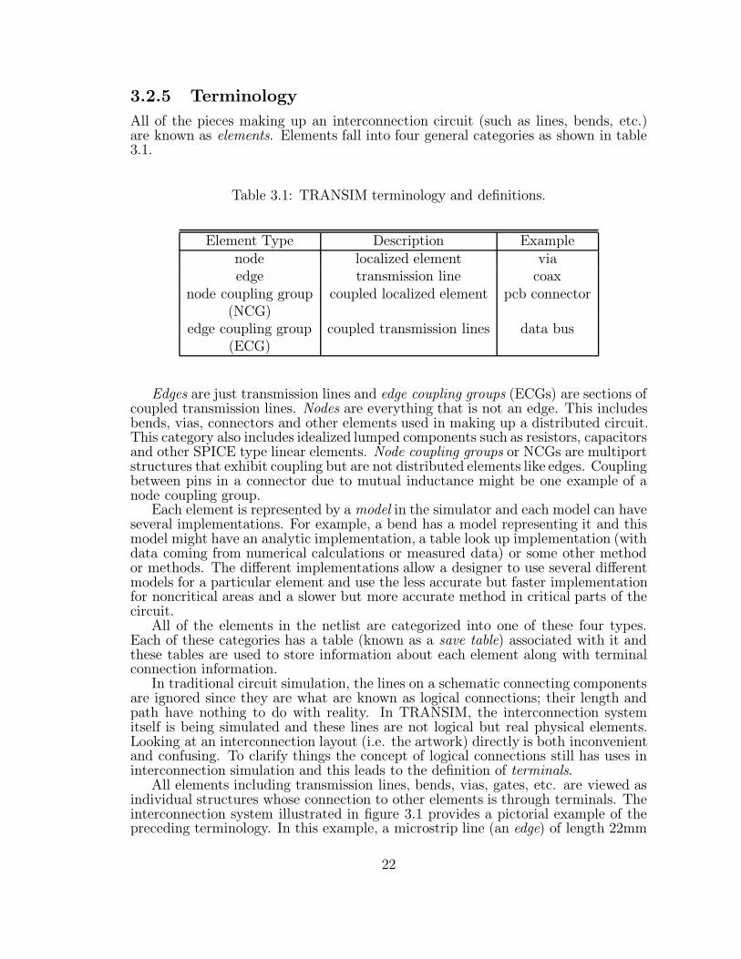
3.2.5 Terminology
All of the pieces making up an interconnection circuit (such as lines, bends, etc.)are known as elements. Elements fall into four general categories as shown in table3.1.
Table 3.1: TRANSIM terminology and definitions.
Element Type Description Examplenode localized element viaedge transmission line coax
node coupling group coupled localized element pcb connector(NCG)
edge coupling group coupled transmission lines data bus(ECG)
Edges are just transmission lines and edge coupling groups (ECGs) are sections ofcoupled transmission lines. Nodes are everything that is not an edge. This includesbends, vias, connectors and other elements used in making up a distributed circuit.This category also includes idealized lumped components such as resistors, capacitorsand other SPICE type linear elements. Node coupling groups or NCGs are multiportstructures that exhibit coupling but are not distributed elements like edges. Couplingbetween pins in a connector due to mutual inductance might be one example of anode coupling group.
Each element is represented by a model in the simulator and each model can haveseveral implementations. For example, a bend has a model representing it and thismodel might have an analytic implementation, a table look up implementation (withdata coming from numerical calculations or measured data) or some other methodor methods. The different implementations allow a designer to use several differentmodels for a particular element and use the less accurate but faster implementationfor noncritical areas and a slower but more accurate method in critical parts of thecircuit.
All of the elements in the netlist are categorized into one of these four types.Each of these categories has a table (known as a save table) associated with it andthese tables are used to store information about each element along with terminalconnection information.
In traditional circuit simulation, the lines on a schematic connecting componentsare ignored since they are what are known as logical connections; their length andpath have nothing to do with reality. In TRANSIM, the interconnection systemitself is being simulated and these lines are not logical but real physical elements.Looking at an interconnection layout (i.e. the artwork) directly is both inconvenientand confusing. To clarify things the concept of logical connections still has uses ininterconnection simulation and this leads to the definition of terminals.
All elements including transmission lines, bends, vias, gates, etc. are viewed asindividual structures whose connection to other elements is through terminals. Theinterconnection system illustrated in figure 3.1 provides a pictorial example of thepreceding terminology. In this example, a microstrip line (an edge) of length 22mm
22

Figure 3.1: Microstrip interconnect example demonstrating nodes (bends) and cou-pled lines.
is connected between terminals 1 and 2. A microstrip bend (a node) connectingmstrip1 and mstrip2 is shown connected between terminals 2 and 3. A pair ofedges are shown connecting terminals 5 and 6 and terminals 8 and 9. Depending onthe spacing between them and other factors, these lines could be two separate edgesor a coupled microstrip line group. In this example they represent the latter andare referred to within TRANSIM as an edge coupling group (or ECG). Finally, thedevices between terminals 6 and 10 and 7 and 11 are nodes (perhaps representing aconnector) which link the coupled lines to a pair of gates. In this example the nodesare coupled together and are referred to as a node coupling group (or NCG).
3.3 Convolution Technique
The general interconnection problem can be broken up into a linear subcircuit (con-taining all of the interconnection elements) and a nonlinear subcircuit (which con-tains the loads). The interconnection subcircuit elements are represented within thesimulator as a set of multiport admittance parameters. The entire interconnectionsystem is represented by a single time domain admittance parameter matrix. Theindividual y(t)’s are just the inverse Fourier transform counterparts to their fre-quency domain form. It is the frequency domain form (y(f)) that are calculated bythe individual element models used by the simulator produce results for.
The transient analysis algorithm’s mathematics can be derived with the aid offigure 3.2. As shown, the general interconnection circuit can be split into linear,matching and nonlinear subcircuits. Here vj and ij are the node voltage and currentat port j, v′j and i′j are the voltage and current at the virtual port j′, and N is thenumber of external ports in the linear subcircuit.
The voltages and currents are related by
v′i(t) = vi(t)− ii(t)Zm i = 1, N (3.1)
andvi(t) = i′i(t)Zm i = 1, N (3.2)
The total transient response is determined by convolving the voltage sources atthe ports of the linear subcircuit with the time domain impulse responses of the
23

Figure 3.2: Partitioning of interconnection circuit into linear and nonlinear subcir-cuits, transient analysis development.
network. Therefore the total transient response at port i of an interconnectionsystem to a voltage vj(t) is
i′i(t) = −N∑
j = 1
∫ t
−∞y′ij(t− τ )v′j(τ )dτ (3.3)
where
y′ij(t) =1
∆tF−1
[Y ′ij(ω)
](3.4)
is the impulse response at port i, time t to a Dirac delta at port j and time t = 0.The linear subcircuit at this point is not the original subcircuit but has been
modified with half of the matching network and therefore Y ′i j(ω) is
Y′(ω) =(Y−1(ω) + ZMI
)−1− 1
ZMI (3.5)
Equations (3.2) and (3.3) can be combined to obtain
vi(t) = −ZMN∑
j = 1
∫ t
−∞y′ij(t− τ )v′j(τ )dτ (3.6)
The transient analysis is performed using this convolution to match the nodevoltage vi(nt) given by (3.6) to the node voltage vj(nt) in (3.1) for all i = j. Indiscrete iterative vector form, (3.1) becomes
kV′(nt) = kV(nt)− kI(nt)ZM (3.7)
where V′ = [v′1,v′2, ...v
′N], V = [v1,v2, ...vN] and I = [i1, i2, ...iN] and equation
(3.6) becomes
kvi(nt) = ZMN∑
j = 1
nt∑nτ = 0
y′ij(nt − nτ ) kv′j(nτ ) +NT∑
nτ = nt + 1y′ij(nτ )
kv′j(0)
(3.8)
24

Here NT is the number of total number of time points, t = ∆tnt and τ = ∆τnτ . Invector form this is
kV(nt) = −Λ kV′(nt)− α(nt) (3.9)
The α(nt) term is a vector with elements
αi = ZMN∑
j = 1
nt − 1∑nτ = 0
y′ij(nt − nτ ) v′j(nτ ) +NT∑
nτ = nt + 1y′ij(nτ) v
′j(0)
(3.10)
By definition v′j(n) = v′j(0) for n < 0. Furthermore, αi can be simplified such that
αi =N∑
j = 1
Nt∑nτ = 1
y′ij(nτ )v′j(nt − nτ)Zm
=
N∑j = 1
Nt∑nτ = 1
gij(nτ ) (Vj(nt − nτ )− Ij(nt − nτ )Zm)
(3.11)
It should also be noted that αi does not change from one iteration to the next(i.e. k to k+1), which is important in reducing the amount of computation requiredat each time point.
Finally, Λ is a matrix with elements
λij = ZMy′ij(0) (3.12)
The iterative cycle is completed by determining k+1I(nt) from k+1V (nt) usingthe nonlinear element models. The next voltage vector in the iteration, k+1V (nt) is
chosen such that |V(nt)− V(nt)| is minimized. This means
k+1V(nt) = kV(nt)− J−1(kV(nt)− kV(nt)
)(3.13)
where J is the Jacobian of (kV(nt)−kV(nt)) with respect to kV(nt) and has elements
Jil = 1− ∂ k vi(nt)
∂ kvl(nt)
= 1− ZMN∑j=1
y′ij(0)ZM∂ kv′j(nt)
∂ kvl(nt)
= 1 + ZM
N∑j=1
j 6=l
y′ij(0)ZM∂ kij(nt)
∂ kvl(nt)
− y′il(0)
(1− ZM
∂ kil(nt)
∂ kvl(nt)
) (3.14)
Iteration continues until |kV(nt)− kV(nt)| < ε where ε is some small number.In most interconnection networks, there is no direct connection between the ex-
ternal ports (there is at least a very short length of transmission line an inductance
25

or a capacitance) and by assuming that all of the ports are instantaneously decou-pled, the above can be greatly simplified. Instantaneously decoupled implies thaty′ij(0) = 0 for i 6= j. This simplifies Λ to a diagonal matrix with elements
λii = Zmy′ii(0) (3.15)
and (3.9) becomes
kvi(nt) = ZMy′ii(0)
[kvi(nt)− kii(nt)ZM
]+ αi(nt) (3.16)
Furthermore, J is also becomes a diagonal matrix with elements
Jii = 1− ZMy′ii(0)
(1− ZM
∂ kii(nt)
∂ kvi(nt)
)(3.17)
Finally, (3.13) reduces to
k+1vi(nt) = kvi(nt)− γii(kvi(nt)− kvi(nt)
)(3.18)
where
γii =
[1− ZMy′ii(0)
(1− ZM
∂ kii(nt)
∂ kvi(nt)
)]−1
(3.19)
3.3.1 Example
For a two port network (such as a single transmission line connecting a load to agenerator) the above equations can be simplified even further with (3.7) becoming
kv′1(nt) = kv1(nt)− ki1(nt)ZM (3.20)
andkv′2(nt) = kv2(nt)− ki2(nt)ZM (3.21)
Equation (3.9) becomes
kv1(nt) = −ZMy′11(0) kv′1(nt)− α1 (3.22)
andkv2(nt) = −ZMy′22(0) kv′2(nt)− α2 (3.23)
The Newton iteration scheme used to find the port voltages at each time stepbecomes
k+1v1(nt) = kv1(nt)−[1 + ZMy
′11(0)
(1− ZM
∂ ki1(nt)
∂ kv1(nt)
)]−1 (kv1(nt)− k v1(nt)
)(3.24)
and
k+1v2(nt) = kv2(nt)−[1 + ZMy
′22(0)
(1− ZM
∂ ki2(nt)
∂ kv2(nt)
)]−1 (kv2(nt)− k v2(nt)
)(3.25)
26

Assuming for this example that a voltage source e1 is connected to port 1 througha linear series resistance R1 and the line is terminated with a linear resistance R2 atport 2, the above implies the following set of equations
kv′1(nt) = kv1(nt)− ZM(e1(nt)− kv1(nt)
)/R1 (3.26)
kv′2(nt) = kv2(nt)− ZM kv2(nt)/R2 (3.27)
kv1(nt) = −ZMy′11(0) kv′1(nt)− α1 (3.28)
kv′2(nt) = −ZMy′22(0) kv′2(nt)− α2 (3.29)
Using αi as given in (3.11), the Newton iteration for this two port examplebecomes
k+1v1(nt) = kv1(nt)− [1 + ZMy′11(0) (1− ZM/R1)]
−1(kv1(nt)− kv1(nt)
)(3.30)
k+1v2(nt) = kv2(nt)− [1 + ZMy′22(0) (1− ZM/R2)]
−1(kv2(nt)− kv2(nt)
)(3.31)
3.4 Thresholding
One of the drawbacks to convolution techniques has always been the large numberof floating point operations used for each time step and for most kinds of transferfunctions there is no way around this fact.
For interconnection structures modeled with time domain admittance parame-ters, the form of the transfer function lends itself to some short cuts when it comes tocomputing the convolution. Looking at a typical time domain response, y(t) (herebyknow as the impulse response) shown in figure 3.7 (the solid line) it is apparent thatmost of the response hovers around the zero-axis with occasional spikes or impulsesrising above the majority of the points. Because of the finite bandwidth used incalculating the frequency domain admittance parameters, there is a certain amountof aliasing noise associated with the inverse Fourier transform process (known asGibb’s phenomenon [11]). which accounts for the very small but nonzero nature ofthe data between impulses. Increasing the number of frequency points reduces thelevel of the aliasing noise but never removes it entirely. This aliasing noise has theeffect of introducing a very slight ripple or ringing to the result of the convolutionwhen the input signal is a fast (or zero) rise time pulse.
Rather than arbitrarily increasing the number of frequency points used whichwould only increase the number of time points in the impulse response, the conceptof thresholding has been introduced which both reduces the number of points usedin the convolution calculations and minimizes the effect of the aliasing noise.
The idea behind thresholding is to select some relative value (vr, 0 ≤ vr < 1)such that any points in the impulse response who’s absolute value is greater thanthis amount are kept for use in the convolution and any points falling below thisvalue are discarded. Mathematically this can be expressed as:
27

y′(t) = y(t), |y(t)| ≥ ε (3.32)
= 0, |y(t)| < ε (3.33)
where y′(t) is the new impulse response and ε is related to the relative thresholdlevel vr by ε = vrymax(t). with ymax(t) being the maximum absolute value of y(t).
The new impulse response looks like that shown in figure 3.3 (b). Obviouslynothing is gained by this if a simple convolution formula is used since the samenumber of floating point operations would be performed, just that a lot of themwould be multiplies by zero. Instead, a record is kept of each nonzero value iny′(t) noting it’s location in the original response y(t). The result of the convolutionbetween indexed points is assumed to be zero and no operation takes place duringthose periods.
In practice, thresholding can reduce the number of points in the impulse responsefrom several thousand to a few hundred and for lossy interconnections the numberof points can reduce below a hundred.
3.5 Errors Introduced by Thresholding
Unfortunately not all of the data below the threshold level is aliasing noise; somereal data is discarded as well, resulting in errors in the finally results that can besignificant for large threshold levels.
3.5.1 DC Normalization
To compensate for these errors, a method known as DC Normalization was intro-duced to help reduce the error or difference between a response calculated with y(t)and one calculated with y′(t). The goal was to reduce the steady state or DC errorbetween the two responses, hence the name.
If a unit step is convolved with y(t), see figure 3.3 (a) (i.e. v(t) = u(t− t0)?y(t)),the output v(t) will be some transitory shape rising from zero and settling down tosome steady state value (see figure 3.4 (c) solid line). The result when u(t − t0) isconvolved with y′(t), see figure 3.3 (b) (v′(t) = u(t− t0) ? y′(t)) is a waveform thatinitially follows the original waveform (to some degree) but eventually diverges to adifferent steady state value than v(t) (3.4 (c) dashed line).
To correct for this long term steady state error, a correction factor can be appliedto all the nonzero terms in y′(t) such that the ’d.c.’ levels match. The correctionfactor can be determined by performing the two convolutions, finding the averageerror between the two and subtracting this average error from the nonzero terms ofy′(t). (Actually there are only nonzero terms in y′(t) since no information is storedfor subthreshold values.) The two convolutions (v(t) and v′(t)) are:
v(t) = u(t) ∗ y(t) =
t∫0
u(τ )y(t− τ )dτ (3.34)
In discrete form this is:
v(t) =k=nt∑k=0
u(k)y(t− k) (3.35)
28

-0.06
-0.04
-0.02
0
0.02
0.04
0.06
0.08
0.1
0.12
0.14
0.16
0 100 200 300 400 500 600(a)
-0.06
-0.04
-0.02
0
0.02
0.04
0.06
0.08
0.1
0.12
0.14
0.16
0 100 200 300 400 500 600(b)
Figure 3.3: Example of typical impulse response (y(t)) with and without thresholding((a) and (b) respectively).
29

0
0.5
1
1.5
2
2.5
3
0 100 200 300 400 500 600
unthresholded y(t)thresholded y(t)
(c)
Figure 3.4: Unit step convolved with thresholded, y′11(t) and unthresholded, y11(t)impulse responses.
30

=k=nt∑k=0
y(t− k) (3.36)
=k=nt∑k=0
y(k) (3.37)
The same can be shown for y′(t) such that
v′(t) =nt∑k=0
y′(k) (3.38)
where nt is one of the N discrete time points. If we define the error e as being thedifference between these two values, then
e = v(N)− v′(N) (3.39)
=k=N∑k=0
(y(k)− y′(k))
The average error is then
ea = 1/Nk=N∑k=0
(y(k)− y′(k)) (3.40)
If this value is used as a correction factor to y′(t), then the new impulse responseis
y′′(k) =
y′(k) + ea if y′(k) 6= 00 if y′(k) = 0
Note that ea is added to y′(k) because of the definition of ea in (3.40). It canbe shown that this correction factor indeed compensates for the dc error by findingthe error between v(N) and v′′(N) where v′′(N) is the convolution of y′′(t) with theunit step function.
k=N∑k=0
y(k)− y′′(k) =k=N∑k=0
(y(k)− (y′(k) + ea)) (3.41)
=k=N∑k=0
(y(k)− y′(k))−Nea (3.42)
Substituting (3.40) into(3.5.1) produces
k=N∑k=0
y(k)− y′′(k) =k=N∑k=0
(y(k)− y′(k))−k=N∑k=0
(y(k)− y′(k)) (3.43)
= 0 (3.44)
Thus at least in the long term steady state, the error is reduced. Unfortunatelyfor most interconnection system impulse response matrices this form of error cor-rection is of limited value and a better method has been developed which betterhandles the type of situations found in practice. This new method is discussed inthe next section.
31

-0.001
-0.0005
0
0.0005
0.001
0.0015
0.002
460 465 470 475 480 485 490 495 500 505 510
y(t)
Figure 3.5: Example of ideal continuous impulse response.
3.5.2 Short Term Steady State Error Correction
The impulse response of in interconnection system is exactly that; a series of im-pulses along the time line. Graphs of the impulse response are usually shown asa continuous line connecting the points resulting in a graph like that of figure 3.5(note that this is only one small section of the total response is shown for clarity).Viewing an impulse response in this manner is not really correct since nothing isactually known about the intervals between data points and a more accurate graphwould be like that shown in figure 3.6.
Realizing the impulse response for what it is, it’s easier to visualize what’s hap-pening when the data is thresholded and the shortened version of y(t), y′(t) is usedin the transient analysis.
If a unit step function is convolved with the impulse response, then the resultis just the sum of the past and current responses at each point in time. Figure 3.7shows the result of convolving a unit step with the full impulse response as well asthe result using the thresholded response, y′(t).
The original dc normalization error correction scheme had several problems in-cluding it’s inability to handle short term errors and the addition of the error correc-tion factor to all of the points in y′(t), distorting the original data. The only pointswhere the y(t) and y′(t) agree are when the values of y(t) are above the thresholdand the only points the error correction factor effects are these same points.
The situation can best be understood by examining figures 3.7 and 3.8. The firstfigure shows the convolution of y(t) and y′(t) with a unit step. The long term steady
32

-0.001
-0.0005
0
0.0005
0.001
0.0015
0.002
460 465 470 475 480 485 490 495 500 505 510
y(t)
Figure 3.6: Example of discrete impulse response used in TRANSIM.
state error is readily apparent by the end of the graph. The second graph shows theconvolutions but with y′′(t) instead of y′(t) where y′′(t) is the dc normalized form ofy′(t). By the end of the graph, the two response do indeed converge but not withoutlarge difference along the way, especially near large Dirac delta like impulses.
These short term steady state (STSS) errors arise when a group of impulses in they′(t) vector capture mostly data points going in one direction (positive or negative)but miss one or more impulses that go in the opposite direction because they don’tquite reach the threshold level (known as subthreshold impulses). Figure 3.9 showsan example of this. Clusters of impulses separated by regions of zero level data areknown as bin groups and such groups that match the above description have netpositive or negative average whereas the same cluster from the original vector wouldhave a net zero response. Assuming of course that this y(t) cluster contained someof these subthreshold impulses missed in the thresholded bin group.
Since y′(t) = 0 for regions between bin groups, the STSS error gets stretched outuntil the next bin group since there is nothing to alter it’s level. If this next groupalso has a net offset and it’s in the same direction as the previous one, the effectsare compounded and the error over the next region increases still further.
In the second error correction method (known as the short term steady state errorcorrection or STSS method), running sums of y(t) and y′(t) (representing the unitstep convolution) are calculated and the short term errors between these calculatedvectorized are minimized. The idea is to determine the convolutions
v(t) =∫ t
0y(τ )dτ (3.45)
33

-0.012
-0.01
-0.008
-0.006
-0.004
-0.002
0
0 200 400 600 800 1000 1200
w/o thresholdingw thresholding
Figure 3.7: Unit step convolved with thresholded and unthresholded y12(t) impulseresponse.
34

-0.012
-0.01
-0.008
-0.006
-0.004
-0.002
0
0 200 400 600 800 1000 1200
w/o thresholdingw thresholding and dc norm
Figure 3.8: Unit step convolution with y12(t) and DC normalized y′12(t).
v′(t) =∫ t
0y′(τ )dτ (3.46)
and use them to determine STSS correction factors. Since the STSS error takes placeduring periods between bin groups, an error term must be found that characterizesthis deviation.
An average error for such a region can be found by integrating the differencebetween v(t) and v′(t) over some period and dividing by that period. If e is theaverage error over the period from t1 to t2 then:
e =1
t2 − t1
∫ t2
t1(v(τ )− v′(τ ))dτ (3.47)
=1
t2 − t1
[∫ t2
t1v(τ )dτ −
∫ t2
t1v′(τ )dτ
](3.48)
In discrete form this becomes
e =1
t2 − t1
t2∑j=t1
[v(j)− v′(j)] (3.49)
35

-0.001
-0.0005
0
0.0005
0.001
0.0015
0.002
400 420 440 460 480 500
y(t) w/o thresholdingy(t) w thresholding
threshold level
bin groups
Figure 3.9: Definition of impulse response bin groups.
But v(t) =∑tk=0 y(k) and v′(t) =
∑tk=0 y
′(k) Therefore
e =1
t2 − t1
t2∑j=t1
j∑k=0
y(k)−j∑
k=0
y′(k)
(3.50)
=1
t2 − t1
t2∑j=t1
j∑k=0
y(k)− y′(k)
(3.51)
The starting and ending points (t1 and t2) are determined by the beginning andending of successive bin groups. Looking at figure 3.13, the first interval would bebetween b1 and a2, the next between b2 and a3, etc. Since the bin groups are the onlyregions wherein the original and thresholded impulse responses match, it is desirableto alter this arrangement as little as possible. Therefore the error correction factoris applied to the last bin in the preceding bin group of the two group sequence. Notethat the running sum,
∑jk=0 y(k)−y′(k) must be calculated for each STSS region since
the error correction of a previous bin group must be accounted for in determiningthe next error correction factor. Figure 3.10 shows the unit step convolution thatresults using y(t) and the STSS corrected y′(t).
An example showing the effects of thresholding and the two methods of STSSerror correction are shown in figure 3.11 for the clock distribution circuit shown infigure 5.14. The two graphs show the response at one of the loads due to a single pulse
36

-0.012
-0.01
-0.008
-0.006
-0.004
-0.002
0
0 200 400 600 800 1000 1200
w/o thresholdingw thresholding andstss error corr.
Figure 3.10: Unit step convolved with y12(t) and STSS corrected y′12(t).
at the input to the clock distribution network. The curve labeled 1 is that calculatedusing the complete impulse response vector for each element of the response matrix.The curve label 2 is the response using thresholded impulse response vectors butwith no error correction. Curve 3 is the same except that dc normalization wasused to correct for the thresholding induced errors. Finally, curve 4 shows thesame response except that STSS error correction was used. One of the problemsof the dc normalization method mentioned in the previous section is evident in thisfigure. Since all of the points in y′(t) were altered by the dc normalization correctionfactor, the maximum and minimum values have been changed and thus curve 3doesn’t reach the STSS values obtained by either the full response or the STSS errorcorrected response. Since one of main reasons interconnection simulations are run isto determine whether significant voltages levels have been obtained to switch a gateon or off, obtaining accurate maximum and minimum values is critical.
Additionally, short term events such as those in figure 3.12 maintain the sameapproximate shape and duration with the STSS method and don’t get stretchedout as with the dc normalization technique. The STSS method will reduce theerror introduced by thresholding but can’t completely eliminate it. While much ofthe discarded data is low level aliasing noise, some of it is actual interconnectioninformation which would otherwise have a small but nontrivial effect on the overallresults. The worst errors arise when a number of bins in a group lie just below thethreshold level (see figure 3.13 bin group 4). The effect of a group of subthresholdvalues on the complete response is to provide a gradual tapering of the signal (see
37

-2
-1.5
-1
-0.5
0
0.5
1
1.5
2
2.5
3
0 1e-09 2e-09 3e-09 4e-09 5e-09 6e-09 7e-09 8e-09 9e-09 1e-08
1 w/o thresholding2 w thresholding w/o error cor.3 w thresholding w dc norm.4 w thresholding w stss error cor.
1
2
3
4
Figure 3.11: Comparison of thresholding error correction methods for port 8 ofreduced clock distribution circuit.
38

-0.5
0
0.5
1
1.5
2
2.5
3
0 1e-09 2e-09 3e-09 4e-09 5e-09 6e-09 7e-09
1 w/o threshold2 w threshold and dc norm3 w threshold and stss e.c.
1
2
3
Figure 3.12: Comparison of threshold error correction methods ability to handleshort term events.
figure 3.14). Since the STSS correction effects the last bin in a group of super-threshold impulses, the STSS value may be correct but the rise and fall times can bedistorted. While this distortion is of some concern, it is more acceptable in naturethan the severer distortions introduced by the dc normalization method.
3.5.3 Comparison of DC normalization vs. STSS error cor-rection methods
This section compares results obtained simulating the same netlist using:
• No thresholding (gold)
• Thresholding but no error correction
• Thresholding with DC normalization error correction
• Thresholding with STSS error correction
Relative error for given threshold level
The first set of experiments examined the relative error introduced by thresholdingalong with the ability of the two correction methods to reduce this error. The output
39

threshold level
a b1 1 a b2 2 a b3 3a4 b4
group 1 group 2 group 3 group 4
Figure 3.13: Effect of threshold level on bin group formation.
-1.5
-1
-0.5
0
0.5
1
1.5
2
0 1e-09 2e-09 3e-09 4e-09 5e-09 6e-09 7e-09 8e-09 9e-09 1e-08
w/o thresholdw threshold and stss correction
Figure 3.14: Effect on output of subthreshold bin group components during transientanalysis.
40

waveforms for the above four cases were collected and the mean square averagebetween the three thresholded cases and the gold standard computed using the meansquare value of the difference between each pair of waveforms using equation 3.52.
σ = 1/N√∑N
i=0
[Vi − V ′i] (3.52)
Here Vi is the gold standard waveform and V ′i is the waveform produced by one ofthe thresholded cases and N is the total number of time points in each waveform.
Since there are multiple waveforms resulting from each simulation, the worstcase mean square average case was chosen as being that netlist’s error metric. Table3.2 shows the worst case mean square average errors for various netlists as shownin chapter 5. For most netlists the DC normalization method of threshold errorcorrection produced relatively little improvement over having no error correction atall. There was a substantial improvement with the STSS method resulting in errorreduction ranging from 38% to 88% with an average improvement of 68%.
Table 3.2: Mean square error of various netlist simulations using DC normaliza-tion and STSS threshold error correction methods versus non-thresholded (gold)simulations
Circuit No Error DC Norm. STSSFigure Description Correction Correction Correction Improvement
5.4 Microstrip 0.00377 0.00383 0.000233 39.2%5.17 Coupled 0.00134 0.00135 0.000285 78.9%
Microstrip5.12 Microstrip 0.00252 0.00236 0.000365 84.5%
w/bends5.21 Data Bus 0.19 0.0765 0.0476 37.8%5.14 Clock 0.00536 0.00271 0.000336 87.6%
Distrib.
Execution times for given relative error
The other set of experiments involved running the same set of netlists and varying thethreshold level for the DC normalization correction method until the mean squareaverage error between the resulting waveforms and the gold standard matched thoseusing the STSS method (which used the original threshold level). Since the STSSmethod consistently showed a lower σ2 value than the DC normalization measure,a lower threshold level was required for the DC case, resulting in longer executiontimes. Table 3.3 shows the execution times for the unthresholded, DC normalizedand STSS cases along with the percent reduction in execution time of the STSSmethod over the DC normalized method. Note that execution times for the case ofthresholding with no error correction were not shown because the transient analysisexecution time is the same as the DC normalized case. Transient execution time isdependent on the number of bins in the impulse response and this number is thesame for both the non-error corrected case and the DC normalization method.
41

Table 3.3: Comparison of transient analysis execution times for DC Normalizationand STSS error correction methods.
Circuit Description DC Norm. STSS Error ImprovementFigure Error Correction Correction
5.4 Microstrip 15s 1s 93.3%5.17 Coupled 8s 3s 62.5%
Microstrip5.12 Microstrip 13s 2s 84.6%
w/bends5.21 Data Bus 167s 65s 61.1%5.14 Clock 2169s 762s 64.9%
Distrib.
3.5.4 Execution Times and Average Error for Different Thresh-old Levels
This set of simulations used the same circuit (the reduced clock distribution circuit)but varied the relative threshold level for each run. The threshold level was variedover a range of 0 to 0.25 and execution times and mean square error (as compared tothe nonthresholded case) data collected. Figure 3.15 shows the mean square error asa function of threshold level and figure 3.16 shows the transient analysis executiontime for the same set of threshold levels.
3.5.5 STSS Error Correction; Conclusions
The STSS method substantially decreases transient analysis execution times by al-lowing relatively high thresholding levels to be used with little sacrifice in accuracy.Unlike the DC normalization method, the STSS algorithm maintains the maximumand minimum values found in the non-thresholded (full) simulations. It also keepsthe general shape of the full simulation waveforms, including brief glitches withoutartificially stretching or truncating them.
Without thresholding, the convolution times involved in the transient analysiscode could be prohibitive and the use of thresholding without some form of errorcorrection introduces such distortion in the output waveforms as to render the resultsuseless.
Convolution techniques have often been ignored because of the large computa-tionally requirements of simplistic “textbook” implementations. By taking advan-tage of the impulsive behavior of interconnect circuits, the combination of thresh-olding and STSS error correction makes the convolution technique practical.
42

0
0.002
0.004
0.006
0.008
0.01
0.012
0 0.05 0.1 0.15 0.2 0.25
Mea
n S
quar
e E
rror
Relative Threshold Level
’f:errs.dat’
Figure 3.15: Mean square error versus relative threshold level for reduced clockdistribution circuit.
0
100
200
300
400
500
600
700
0 0.05 0.1 0.15 0.2 0.25
Tra
nsie
nt A
naly
sis
Tim
e (s
ec)
Relative Threshold Level
’f:times.dat’
Figure 3.16: Transient analysis time versus relative threshold level for reduced clockdistribution circuit.
43

Chapter 4
Implementation in a Circuit Simulator
4.1 New Convolution Method
Both the scattering and admittance parameter approaches require the use of aninverse FFT function since the interconnection network is best simulated in thefrequency domain (conduction and dielectric losses are frequency dependent phe-nomena) and the nonlinear analysis is best handled in the time domain. Any timea Fourier transform is used (in this case an inverse FFT), the input signal must beband limited to prevent aliasing. The limiting can be done artificially by filteringor can result naturally from the properties of the input signal. In the case of scat-tering parameters the transmission coefficient, S12, is naturally band limited for asufficiently lossy line. Therefore |S12| → 0 as f → ∞. The reflection term S11, onthe other hand, approaches one as frequency increases (|S11| → 1 as f →∞). Thusperforming an inverse FFT on a sufficiently lossy line has little aliasing in the S12
term but almost always results in sever problems for S11.S11 can be filtered prior to the FFT operation but this requires the use of some
high order low pass filter which can introduce large phase distortions in the resultingsignal. By way of a graphical example figure 4.1 shows unfiltered and filtered scat-tering parameters for a single low loss line. Only two of the network parameters aredistinct because of symmetry. For this example a coaxial airline with the followingparameters was used. Inner radius 0.5mm, outer radius 1.14mm, tand was 10−5
and σ = 5.8x10⁷. The results were calculated using MathCAD 3.0. A constant d.c.resistance and conductance of 10−7Ω and 10−71/Ω respectively were used to keepthe numerical results of one of the steps from becoming singular at d.c. The filteringwas performed using a simple second order lowpass filter with a 3db frequency of 40Ghz.
While filtering of the scattering parameters reduces or eliminates the alias-ing problem, the question remains as to what is the physical result of filtering s-parameters as there is no physical basis for such an abstraction.
With frequency domain admittance parameters y(f), a self limiting conditioncan be found when the complete picture of the problem is grasped. Since the objectof these simulations is to model electronic packaging structures composed of aninterconnection transmission network and device loads, the last structure connectingthe lines to the loads (inputs to gates for example) can’t be ignored.
As seen in figure 4.2, there is an I/O pad terminating the transmission line anda bond wire connecting the pad to the integrated circuit.
Since the bends and vias making up the interconnection system are modeled, thisfinal stage must be modeled as well. In it’s simplest case, the packaging structureassociated with the pad and bond wire can be modeled as a simple lumped elementLC model.
For the case of a simple microstrip line connecting two devices, the actual struc-ture is figure 4.4 with the corresponding electrical model of figure 4.5.
The admittance parameters of this new structure (both y11 and y12) go to zero as
44

0
0.05
0.1
0.15
0.2
0.25
0.3
0.35
0.4
0.45
0 1 2 3 4 5 6 7 8 9 10
x10 Ghz
S11 Unfiltered
S11 Filtered
(a)
0.1
0.2
0.3
0.4
0.5
0.6
0.7
0.8
0.9
1
0 1 2 3 4 5 6 7 8 9 10
x10 Ghz(b)
S12 Unfiltered
S12 Filtered
Figure 4.1: Effect of required filtering on two port S-parameters.
45

Figure 4.2: Chip to substrate bondwire connection
Figure 4.3: Lumped element mode of bondwire parasitics.
frequency increases since the inductance shows a higher impedance as frequency rises,approaching an open circuit and the capacitance drops in impedance, approachinga short circuit.
The introduction of this packaging network does not help the scattering param-eter case since |S11| still approaches one as frequency increases. |S12| will approachzero faster with the packaging network than without but |S12| was not the mainproblem in the first place.
That |S11| approaches one can be seen by looking at figure 4.6. As ω increases,ZL = jωL rises and ZC = 1/jωC falls resulting in the circuit shown. The reflectioncoefficient [10] for large ω becomes
|Γ|ω→∞ →∣∣∣∣ZC − Z0
ZC + Z0
∣∣∣∣→ ∣∣∣∣−Z0
Z0
∣∣∣∣ = 1 (4.1)
Therefore the scattering parameter reflection term, |S11| approaches one as ω in-creases.
The introduction of the packaging elements alleviates the aliasing problem butstill doesn’t address the infinite impulse response issue. Since the packaging lumpedvalues (L and C) are ideal, they introduce no loss to the system and if the transmis-sion line is ideal or low loss, the impulse problem remains. Borrowing from the ini-tial concept behind using time limited scattering parameters, a reference impedanceother than a short circuit is used. At each reflection, energy is dissipated and theimpulse response decays rapidly with time. By introducing the network shown in
46

Figure 4.4: Simple two port interconnect
Figure 4.5: Simple interconnect with parasitics
figure 4.7, the impulse response calculated from the new interconnection structurewill no longer be infinite in duration, even for a lossless line.
4.2 Band Limiting and Alias Control
The starting point for the new method is to divide the circuit into two major sub-circuits so that this new augmentation network can be used. The first subcircuitcontains all of the linear elements and the other contains all of the nonlinear ones.An example of this is shown in figure 4.8.
The need to perform interconnection structure calculations in the frequency do-main as well as the desire to handle arbitrary nonlinear loads leads to the use of
Figure 4.6: Effect of parasitics at high frequencies.
47

Figure 4.7: New augmentation networks applied to simple interconnect circuit.
Figure 4.8: Partitioning of general interconnection circuit into linear and nonlinearsubcircuits.
48

Figure 4.9: Interconnect circuit with addition of simple lumped element parasiticmodel.
convolution techniques. While simple in theory, the use of convolution mixed withfrequency domain representation of the interconnection network posses a doublelimit problem.
As mentioned in previous sections, convolution methods have problems dealingwith low or no loss lines. This situation can lead to an infinite impulse responsefor the line and a corresponding infinite computation time to do the convolution.Therefore, some way must be found to keep the length of the impulse response asshort as possible if the technique is to have any validity.
Since the interconnection data is initially in the form of frequency domain pa-rameters, the time domain impulse response is obtained by performing a FFT (FastFourier Transform) on the individual admittance parameters. Unfortunately theFFT assumes that the input signal is periodic and if the signal is not sufficientlybandlimited aliasing will occur. Therefore some form of filtering must be done toband limit the parameters prior to performing the FFT. Merely adding a filteringstage can introduce an artificial shape to the parameters and cause severe phasedistortion that is nonphysical in nature.
The problem is especially apparent when dealing with scattering parameters asseen in figure 4.1. Here the two frequency domain s-parameters describing a simplelow loss line are shown in their filtered and unfiltered forms (only two s-parametersare necessary to describe the line because of symmetry). The figure 4.1 (a) showsthe reflection factor |S11(f)| filtered and unfiltered and figure 4.1 (b) shows the sameexcept for |S12(f)|. Note that |S12(f)| naturally decays toward zero with increasingfrequency and would fall faster for a higher loss line. Artificial filtering of thisparameter leads to a faster rolloff but importantly, the trend is the same. Filteringof S11(f) on the other hand leads to a totally different frequency trend since |S11(f)|naturally approaches 1 with increasing frequency. Instead |S11(f)| now forms a humpshaped response that does not have a physical interpretation.
By using admittance parameters instead of scattering parameters and by in-cluding packaging effects, the network parameters used by TRANSIM are naturallybandlimited and don’t require high order nonphysical filtering. Previous intercon-
49

nect analysis methods considered the interconnection structure as primarily a set ofidealized transmission lines connected to an arbitrary load as shown in figure 4.9.
Since TRANSIM is primarily a packaging simulator, idealized components are tobe avoided, requiring a detailed look at how lines and devices are actually connected.In the case of an MCM or PCB there is always a pad terminating the transmissionline and a wire bond, solder ball or some other form of connection wire between thepad and the I/O pad on the integrated circuit. An example of this was mentionedearlier and illustrated in figures 4.2 and 4.3.
The interconnection network including these parasitic elements has a bandlimitedresponse like that shown in figure 4.10. These graphs show the frequency domainadmittance parameters for a simple low loss line (only two are shown because ofsymmetry). Note that the responses of both |y11| and |y12| tend toward zero at theupper frequency end. The parasitic inductances and capacitances were 0.1nH and0.2pF respectively. Values in this range are commonly found in conventional wirebonded I/O pad packaging schemes [14], [15], [40], [41].
4.3 Limiting Impulse Responses
While these packaging parasitics’ bandlimit the frequency domain admittance pa-rameters and minimize the aliasing problem the problem of long impulse responsefunctions remains. With the network shown in figure 4.9 a augmentation networklike that in figure 4.11 can be used to reduce the impulse response length. Withthe addition of the augmentation network the impulse response of the original net-work augmented by the augmentation network is time limited. With this additionalimpedance connected to the ends of the transmission line a short circuit appliedto one end results in the impedance being connected to ground and in the case ofa perfect match (Z = Z0) no reflection occurs and the impulse response length isminimized.
Unfortunately this simple augmentation network no longer works in the intendedfashion with the addition of packaging parasitic’s. A single augmentation impedancenetwork results in aliasing problems for the following reason. The augmentationnetworks are added to (or augment) the reduced nodal admittance matrix (RNA)after the admittance’s at all frequencies have been found. Augmenting by a singleimpedance has the effect of adding constants to the terms of the RNA at all fre-quencies. The upper frequency terms are no longer tend toward zero and aliasingproblems will occur.
This can be seen be examining figure 4.12 (a), a single transmission line connectedto nonlinear loads through parasitic packaging elements. Also included are the twoaugmentation impedances at both ports. The admittance parameters for all linearnetworks in TRANSIM are found initially in the frequency domain and their behaviorat the upper frequencies is important. As ω increases, the inductors begin to looklike opens and the capacitors like shorts, leading to the circuit of 4.12 (b).
Clearly, port 1 is isolated from port 2 and no voltage on port 1 will cause acurrent to flow at port 2 (and vice-versa). Hence
y12 = I1/V2 = 0 (4.2)y21 = I2/V1 = 0 (4.3)
also y11 and y12 are just the input admittances looking in the ports such that y11 =y22 = 1/Z. Therefore y12 and y21 approach zero as ω increases but y11 and y22 do
50

0
0.002
0.004
0.006
0.008
0.01
0.012
0.014
0 2 4 6 8 10 12 14 16
x10 Ghz
y11(f)
0
0.001
0.002
0.003
0.004
0.005
0.006
0.007
0.008
0.009
0.01
0 2 4 6 8 10 12 14 16
x10 Ghz
y12(f)
Figure 4.10: Naturally bandlimited admittance parameters with packaging parasiticsincluded.
51

Figure 4.11: Single element augmentation network.
Figure 4.12: Single impedance augmentation network contribution to aliasing withpackaging parasitics included; (a) is an augmented two port; (b) is the networkbetween ports 1 and 2 at infinite frequency.
not. Unless some form of low pass filtering is performed prior to the FFT, aliasingwill occur in the final y11(t) and y22(t) terms.
With the new augmentation networks shown in figure 4.7, when the the twoimpedances of the augmentation network (being of equal but opposite values) ef-fectively cancel each other out at high frequencies and thus aliasing problems areavoided.
That these two networks cancel each other out can be seen by looking first atthe two impedances in parallel. The impedance of this combined structure is
Z =−ZZZ − Z =∞ (4.4)
which implies an open circuit between node B and ground. The top two impedanceare now in series with a combined impedance of Z−Z = 0, implying a short circuit.Therefore node A is directly connected to node C.
52

The time domain impulse response length will remain limited with this newaugmentation network scheme, and this can be seen by looking at the worst casescenario (figure 4.13) of a short circuit at one end of the line and an ideal Diracdelta generator at the other. Under the ideal case in which there is a perfect matchbetween the line and augmentation impedance there are no reflections at the shortedend of the line because there is a matched load between the line and ground. In theopen circuit case the two impedances at the open circuit end combine to produce ashort to ground. The Dirac delta launched into the line will invert and reflect off thisshort but upon arriving at the generator end, finds a matched impedance to ground(the generator shorts the −Z component to ground) and no further reflections occur.
Figure 4.13: Short circuited ideal lossless line representing worst case infinite impulseresponse problem.
4.4 Nodal Admittance Matrix Formulation
One of the concepts for the packaging simulator is based on the premise that increas-ing available memory is cheaper and easier than increasing processor speed. Thus inTRANSIM memory is used to store model calculations so that they can be reused. Inan interconnect network there are many repeated elements. For example, there arejust a few types of vias, bends and chip connection elements. These are convientlydescribed by admittance parameters. As well, transmission lines, including coupledtransmission line groups, have only a few different cross–sectional geometries but,of course, many different lengths. Thus transmission lines are most convenientlymodeled by their propagation constant, γ and characteristic impedance Z0 as thesecan be calculated once and reused for lines of identical cross section but differentlengths. (Note that for coupled lines, γ and Z0 are matrices.)
The individual admittance matrices are combined to form the total Nodal Ad-mittance Matrix (NAM) as illustrated in figure 4.15. The NAM matrix is N × Nwhere N is the total number of terminals in the circuit. The matrix is then reducedto a M×M matrix (the Reduced Nodal Admittance (RNA) matrix) where M is thenumber of external terminals. The calculation of the transient response occurs afterthe augmentation of the RNA matrix with the augmentation network and conversionto time domain admittance parameters (the impulse responses) and is described indetail in section 4.6.
The admittance parameters for the transmission line systems, as mentioned ear-lier, are calculated from knowledge of the γ and Z0 matrices. These quantities arestored (actually the eigenvalues and eigenvectors of γ are stored for couple lines) in-stead of the admittance parameters because of the pattern repetition found in most
53

interconnection structures. Details on how the admittance parameters for transmis-sion lines and coupled lines are calculated is given in appendix A.
4.5 Packaging Simulator Topology
The packaging simulator developed here supports a limited hierarchy of circuit el-ements. In contrast, a conventional simulator based on the SPICE paradigm allcircuit elements are treated equally. The packaging simulator recongizes four classesof elements
1. edge a single transmission line element which is distinguished by having length.
2. node a conventional element which is treated as a dimensionless element (apoint model). Examples are a resistor, bend, and a via. Every element that isnot a transmission line is a node.
3. edge coupling group (ECG) a set of coupled transmission lines.
4. node coupling group (NCG) a set of nodes that are coupled. For example, aset of adjacent bond wires can be viewed as an NCG.
Each of the elements has terminals which are used to connect various devices to-gether. Note that the usage of the word node differs from that in the SPICEparadigm.
4.6 Implementation of Packaging Simulator
An overview of the packaging simulator implementation in the program TRANSIMis given in figure 4.22.
The first step is to create the element tables which contain pointers to informationstored about each device making up the input netlist. There are four tables, oneeach for nodes, edges, NCG’s and ECG’s.
The input netlist is parsed and information about each element is extractedalong with run time information, output file requests and other parameters. Foreach element in the netlist, it’s type (edge,node, etc.) is determined and a newentry in the appropriate table is created. Physical information about the element(length, width, etc.) is then stored.
1. The input netlist is parsed and tables containing the different element typesare created.
2. Element data structures are created containing space for storage of physicalparameters (length, width, etc.) and calculated data (y(f)) or pointers to thepreviously calculated data from an identical element. The physical data is nowstored for future use.
3. The data calculations are performed. For elements other than transmissionlines, frequency domain admittance parameters are calculated, space is allo-cated and the data stored. Note that this data is stored only once per elementtype. Coupled transmission lines are handled differently from other elements.Instead of admittance parameters, the characteristic impedance matrix Z0 and
54

the eigenvalues and eigenvectors for the complex propagation constant matrix(γ) are stored. For uncoupled lines, the scalar Z0 and γ values are stored.
4. The total nodal admittance matrix describing the interconnection network isbuilt using the individual element parameters. This matrix is M ×M whereM is the total number of terminals in the circuit.
5. A matrix reduction is performed on the NAM matrix to reduce it to an N ×Nmatrix (the RNA, reduced nodal admittance matrix) where N is the numberof external terminals (those tied to loads).
6. The RNA matrix is augmented to include the linear network side of the aug-mentation impedance network.
7. An inverse FFT is performed on each element of the RNA to produce a set oftime domain impulse responses.
8. The time domain responses are subject to thresholding conditions and thereduced impulse responses are stored as sparse vectors along with their corre-sponding time vectors.
9. The transient analysis is performed using the sparse impulse response vectorsand the nonlinear load models. Note that the nonlinear load models need notbe the same for each external node, any combination of load models is allowed.
10. Output processing including mathematical manipulation of the output values(for example, subtract two voltage waveforms) is performed and the resultswritten to files and/or plotted directly to the screen.
The information stored for both nodes and edges is similar enough that only thediagram for node data structures (figure 4.14) is shown. The primary structure is ofthe type gr NodeTab t and is the head of the node table. Each node in the netlistis represented by a structure of type gr NodeTabData t which contains informationabout its origins, terminal connections and a pointer to its’ own information block.This block (of type capNodeParam t contains graphical information (which is notcurrently used), unique element information such as the element name and a descrip-tion string along with a pointer to the device block that contains information aboutthis particular implementation of a model (in this example a bend and a via). Theseblocks are of types unique to the element and contain further information aboutthe element including the size of its returned admittance matrix, any polynomialsassociated with the admittance calculations, physical information (such as width,height, etc.) and finally a pointer to the complex admittance matrix which containsthe calculated admittances for this element. Note that this is a 3D matrix since itcontains 2D admittance matrices at each frequency.
4.6.1 Creating the Nodal Admittance Matrix (NAM)
The first step is to create the sparse nodal admittance matrix. At this point this isjust a 2D flat matrix and contains no data. An example of this structure is shownin figure 4.15 and the following terminology will be used in the NAM build process.The flat matrix mentioned is referred to as the city grid since it loosely resembles arectangular manhattan style grid of streets at right angles to one another. Depending
55

Figure 4.14: Example of table data structures, nodes.
56

on the relationship between different elements some of the grid squares will containdata and others won’t. Since each admittance parameter is a function of frequency,there are columns of data at each filled grid square forming towers (or buildingsusing the city terminology). The pattern of towers making up the cityscape arereferred to as the city floor plan. Note that this is different than the city-grid sincenot every grid square contains an admittance tower. This terminology will becomeimportant in later discussions.
Each table is then searched for elements that have outside terminals (terminalsconnected to a “nonlinear” external device). The term nonlinear is used loosely heresince the load can be defined as a straight line and is actually linear in nature. Sincea matrix reduction will be performed (which works by eliminating outside rows andcolumns), the terminals of the external nodes must be placed or assigned to the firstentries in the NAM. If there are M external loads then the first M entries of theNAM are reserved for these elements.
To simplify the flowchart some duplication of functionality is not shown as indi-cated in the next section of figure 4.22. This same section of flow chart can be usedto describe both the node and node coupling group evaluations. The terms nodeand node coupling group can be used interchangeably in the following description.
4.6.2 Nodes
The first time a node of a particular type is encountered, the vectorized admittanceparameter calculation routine is called and a 3D sub–NAM is produced. This sub–NAM is saved for reuse if this particular type of element is encountered again, Afterthe vectorized call, the contents of the sub–NAM are added to the complete NAMaccording to the method described above.
The next time this element is encountered, the previously calculated and retainedsub–NAM is used to add the effects of the current element to the complete NAM.Since this is a different instance of this element type and resides in a different partof the circuit topology, the sub–NAM elements are added to different bins in theNAM than those used by the first instance of this element type.
The procedure is repeated for each node in the list. If the element has never beenencountered, then the vectorized admittance calculation routine is called. If this isnot the first instance, the previously calculated sub–NAM is used.
The vectorized routines referred to are designed to take advantage of the fre-quency independent nature of some of the intermediate variables used in calculatingadmittances for some of the devices. For linear, homogeneous material, the capaci-tance and inductance of an element such as a bend are frequency independent andit makes sense to put calculations for C and L outside of the frequency loop. Thusonly frequency dependent effects such as resistance (R) and conductance (G) are in-cluded in the frequency loop. A non-vectorized routine would require recalculationof the frequency independent variables on each call resulting in a large number ofunnecessary computations.
4.6.3 Coupled Nodes
Coupled nodes are handled in almost exactly the same fashion as uncoupled nodesexcept that the results of the admittance parameter calculations are matrices largerthan 2 × 2. Other than this, the calculations (model dependent) and inclusion ofthe sub–NAM’s into the complete NAM are handled in the same manner.
57

4.6.4 Edges
Edges (transmission lines) are handled in a slightly different manner to nodes. Sincenodes such as vias are assumed to have a fixed geometry, the admittance matricesfor node elements are constants.
Transmission lines come in a variety of geometries and lengths, both of whichdetermine a particular element instance’s sub–NAM. Even though the same cross-sectional geometry might be used for all of the lines in an interconnection network,the sub–NAM’s will be different because the lines are of different lengths. Thus foredges storing sub–NAM’s is not useful.
The information that is actually retained is dependent on the means by whichthe admittance parameters for a particular line type and length are calculated. Amore detailed description of this method is given in Appendix A but in essence themethod revolves around finding the complex characteristic impedance, Z0 and thecomplex propagation constant, γ and using this information along with a variationon the telegraphers equations to determine the admittance parameters. Since Z0
and γ are independent of length, they only need to be calculated once for each linegeometry. For example, Z0 and γ for a microstrip line are determined by the width,thickness, height and dielectric constant of the substrate and are independent oflength.
4.6.5 Coupled Edges
Coupled edges (sections of coupled transmission lines) are handled in much the samefashion as single edges except that the admittance parameters are calculated in asomewhat different fashion since Z0 and γ are now matrices and computing e−γl ismore difficult because this term is also a matrix. Details of how the admittanceparameters are calculated for coupled lines can be found in Appendix A. BecauseZ0, γ and e−γl are either matrices or vectors, computing the later term is moredifficult and requires information about the eigenvalues and eigenvectors of γ. Sinceγ itself is never used actually used in any of the calculations, it is unnecessary tostore γ itself. Instead, the eigenvalues and eigenvectors of γ are stored and used forelements that have similar geometries but different lengths.
It should also be noted that the admittance calculation method of Appendix A isonly for coupled line structures of equal length. Therefore a section of coupled lineslike that in figure 5.21 must have varying length uncoupled line pieces connectingthe coupled line section with the bends and thus the rest of the interconnectionsystem. More detailed coupling modeling could be performed if either fewer lineswere assumed to be coupled (say using pairs instead of all eight lines) or the extensionlines were assumed to be coupled in smaller groups or pairs. This would allow moreof the bus between the bends to be modeled as coupled lines. Since a majority ofthe coupling occurs over long stretches of closely spaced lines, this is not a seriouslimitation.
4.6.6 Example NAM Build
An example of this build process can be seen in figure 4.15. Here the simple circuitshown at the top consists of five elements (four microstrip lines a,b,c,d and one setof coupled lines, e) but only two of which are unique (the coupled line group and themicrostrip type). The microstrip lines can all be of different length but as long as the
58

physical construction is the same, TRANSIM considers them to be the same element(as far as the save table is concerned). For the microstrip line, the characteristicimpedance Z0 along with γ is stored. For the coupled line group, the same type ofinformation is stored except that Z0 and the eigen system for γ are matrices.
During the build process, this information is used to construct the 3D admittancematrices for each element. For clarity, the microstrip lines are all assumed to be ofthe same length and hence only one 3D subnam matrix is shown. Since microstriplines are two port devices, this matrix is 2× 2× F where F is the number of floorswhich corresponds to the number of frequencies at which admittances are calculated.For the two line coupled line group this matrix is 4× 4× F .
The five sets of sub–NAM’s are combined into the city scape shown which hasa number of vacant city blocks between towers. For circuits with a large numberof devices each of which have relatively few ports, this sparseness will be morepronounced. The degree of sparseness for this example can be seen at the bottomof 4.15 in the city map. Because most circuits contain a high degree of sparseness,a specialized admittance matrix structure was created for TRANSIM by which onlytowers that actually contain data are allocated. The primary matrix is a 2D grid ofpointers to complex vectors. Space is allocated for these vectors only when a toweris to be constructed that will contain admittance parameter information. Otherwisethe 3D matrix would have to be allocated completely in the beginning, potentiallywasting a significant amount of memory. This would result in either reduced circuitcomplexity that TRANSIM could handle or slow execution time as large blocks ofdata would have to be swapped to external storage.
4.6.7 NAM Reduction
The matrix reduction section of TRANSIM uses one of the larger fractions of thetotal execution time (see figure 5.24), depending on the complexity of the cir-cuit and the thresholding level can use a larger fraction than the transient anal-ysis/convolution portion.
The present method of reducing the matrix is a relatively simple general purposemethod that proceeds as follows.
• The diagonal entries are scanned for the largest entry (the self admittance ofmost devices is usually greater than the through admittance) which becomesthe pivot. Examining just the diagonal entries saves N2 − N comparisons(where N is the number of ports).
• Once the pivot is found (A(p, p)), the pth and M th column are exchanged (theM th column is the last column of A to contain nonzero data, in the first passM = N).
• The pth and M th rows are exchanged.
• The new M th row is divided by the A(m,m) element.
• Each row K,K = 0 . . .M − 1 is processed as follows, if Rk indicates row k:
Rk = Rk − CRM (4.5)
where C is theM th element of Rk. In matrix notation: Ai=kj = Akj−Ak,MAM,j
j = 0 . . .M − 1
59

Figure 4.15: Example of NAM construction from subNAM’s showing non-admittance parameter information stored for lines.
60

Figure 4.16: Single row from matrix A.
Figure 4.17: Example M-port device
Depending on the complexity of the circuit, the initial matrix may be quitesparse, especially if there are only two terminal elements (i.e. no tees, coupled lines,etc.). In this case A will have a maximum of three nonzero elements per row orcolumn. This can be seen by examining figure 4.17. Examining the admittancesseen looking from port y, we see the self admittances at port x (y22). We also seetwo through admittances (y21 and y23). These are all of the admittances seen fromthis port. Although y21 = y12 (for reciprocal junctions), y12 is associated with port1 not port x. The third row in A would then be as shown in figure 4.16 (here an Xindicates a nonzero value).
Referring to the 3D manhattan matrix (figure 4.17), we see that initially only N+2(N − 1) towers need to be allocated. Unfortunately as the row/column operationsof the reduction proceed, the empty city blocks will be filled. Which blocks get filleddepend on the layout of the initial sparse matrix and the pivot point. The worstcase occurs when the pivot falls on a row with a large number of nonzero elements.The number of nonzero elements depends on the number of other ports the deviceconnected in at the row in question has. This is best seen by examining the floorplan (figure 4.18) of this network.
Here an X indicates a nonzero value (or at least the potential for a nonzero value)while a blank space indicates a zero. Reading across row y indicates that node y seesadmittances from node x, itself and node 1. Row 1 on the other hand, shows theconnection between node y, itself and all the other nodes connected to this M portdevice. Thus the row with the most nonzero values will be the one that connects aport of the largest multiport device to the rest of the circuit and will have M + 1entries (M = number of ports).
If the pivot falls on one of these rows then this row is eventually propagated tothe bottom of the matrix and is used as the ‘subtraction’ vector from each of theother rows. Thus the processed row may have up to M − 2 filled elements (formerlyzero elements that now contain data). There are M − 2 fills instead of M becausethe last column is being ‘zeroed out’ and fill doesn’t count and there are alwaysdiagonal elements. Symmetry dictates that for a given processable row (say row k)then the subtraction vector will have a corresponding element in the kth slot andthus does not contribute to fill. The NAM after one cycle through the reduction
61

Figure 4.18: City map corresponding to M-port example
process is illustrated in the following set of floor plans indicating one frequency inthe 3D nodal admittance matrix. The circuit that these floors represent is shownin figure 4.19. The first floor plan in figure 4.20 is the initial layout. The diagonalentries are scanned and the largest chosen as the pivot (A(6, 6) in this example).
The last column and row (9) are to be eliminated so the next operation is toswitch the 6th and 9th columns (second floor plan). To maintain the original rela-tionships within the matrix, the 6th and 9th rows are also exchanged (figure 4.21).
Finally, the reduction loop is performed, eliminating the 9th column and row.Note the filled elements indicated by X’s in the second of the two floor plans. Asnoted, the largest fill factor is M − 2 = 5 − 2 = 3 and has shown up on row 5 asindicated. Overall 6 new towers were added to the city to house these new values.As reduction continues, more vectors will be required to store new elements as thematrix shrinks toward the upper left corner.
In the current method, once a vertical tower is built, it is not removed even afterthe reduction has cycled past it (it’s values become zero but the memory locationremain in use). This is because the reduction proceeds from floor to floor, completingthe entire reduction on a floor before moving to the next. Thus even though a flooris finished with it’s part of a tower, floors not yet encountered still have need of theremaining portions of that tower.
The location of the fill factors is unknown in advance since their location dependson the current location of allocated towers as well as the choice of pivot. Further-more, this pivot is not necessarily in the same place from floor to floor (frequencyto frequency) and a space that goes unfilled on one floor may be filled on another.
62

Figure 4.19: NAM reduction example circuit
Figure 4.20: NAM reduction example before and after first pivot, A(6,6).
Figure 4.21: NAM reduction example showing second pivot operations and fill ef-fects.
63

Figure 4.22: TRANSIM flowchart, part 1
64

Figure 4.23: TRANSIM flowchart, part 2
65

Figure 4.24: TRANSIM flowchart, part 3
66

Chapter 5
Results and Comparisons
5.1 Frequency Domain Versus Time Domain Validity Tests
To verify TRANSIM’s transient analysis operation, a comparison between a purelyfrequency domain simulation (using linear loads) was performed. This test used thesingle transmission line circuit shown in figure 5.4. The frequency domain simulationwas caried out using MathSoft’s mathematical modeling software MathCad. Thissoftware allows for simple construction of mathematical models by entering equationson a spreadsheet in standard mathematical notation. It has built-in file manipulationand data analysis functions (such as FFT’s), making it ideally suited to one-of-a-kindtype simulations, such as this. To further simplify the frequency domain simulationa coaxial line was used instead of a microstrip or some other such transmissionline because coaxial lines have relatively simple mathematical descriptions. As seenin the figure parasitic packaging effects are included along with the augmentationnetwork. The augmentation network is used for consistency with TRANSIM.
For the frequency domain model, the general lossy coaxial line was modeled byfirst calculating the RLGC per unit parameters using [10]
L =µ0
2πln(b/a) (5.1)
C =2πε0εrln(b/a)
(5.2)
R =1
2π
(1
a+
1
b
)√µ0ω
2σ(5.3)
G =2πωε0εrtdln(b/a)
(5.4)
where a is the inner radius, b the outer radius, σ is the conductivity of the conductormaterial and td is the loss tangent of the dielectric. The diameters and dielectricconstant were chosen to give a characteristic impedance (Z0) magnitude of 50Ω. Inother words
Z0 =
√R + jωL
G+ jωC(5.5)
The admittance parameters are related to the complex propagation constant (γ) andcharacteristic admittance (Y0) by
y11 =Y0
tanh(γl)(5.6)
y12 =Y0
sinh(γl)(5.7)
67

where l is the length of the line and γ is
γ =√
(R + jωl)(G+ jωC) (5.8)
Since a uniform coaxial line is symmetrical, only two admittance parameters arerequired to characterize it. The complete nodal admittance matrix for the system,including parasitics and augmentation networks can be found using the matrix equa-tion
Y ′ =
[[[Y −1 + ZLI
]−1+ YCI
]−1
+ ZmI
]−1
− YmI (5.9)
where Y =
[y11 y12
y12 y22
], ZL = jωL and YC = jωC. Zm = 1/Ym is the augmentation
network impedances.For the frequency domain calculations a transfer function was derived for the
source and load end voltages and the resulting signals were obtained by multiplyingthe transfer functions by the input signal. The input signal for this test was anideal, time shifted pulse whose frequency response was determined using MathCad’scomplex FFT routines. An analytic expression was not used because it was desirableto change the characteristics of the pulse (rise/fall times, etc.) without having torederive the frequency domain expressions. The resulting signals were transformedback into the time domain using the same FFT.
The transfer functions used were
T1(ω) =1 + 2y11Zm − y2
12ZmZL − y212Z
2m + y2
11ZmZL + y211Z
2m + y11ZL
Td(5.10)
T2(ω) =−y12ZLTd
(5.11)
whereTd(ω) = 1 + 2y11Zm + y11ZS − y2
12ZmZL − y212Zm − y2
12ZSZL
−y212ZSZm + y11ZL + y2
11ZmZL + y211ZSZL
+y211Z
2m + y2
11ZSZm
where ZL and Zm are constants, y11 and y12 are functions of ω. The voltages ateither end of the line were found by
V1(ω) = Vs(ω)T1(ω) (5.12)
V2(ω) = Vs(ω)T2(ω) (5.13)
The same coaxial line and linear load was simulated by TRANSIM and theresulting waveforms are plotted along with the results from the frequency domainmethod. Voltage V1 is shown in figure 5.1 and V2 is shown in figure 5.2. Theresulting waveforms are very similiar with differences due primarily to the numericalroundoff errors in MathCAD’s internal function calls and to the aliasing problemsof converting the time domain input waveform to the frequency domain for themultiplication method. The time domain waveform is used directly by TRANSIMand no effort was made at windowing or otherwise reducing the aliasing effects priorto performing the Fourier transform.
68

-2
-1
0
1
2
3
4
5
6
7
0 1.0 2.0 3.0 4.0 5.0 6.0 7.0
TRANSIM (time domain)MathCad (freq domain)
ns
Figure 5.1: Frequency domain (multiplication method) versus TRANSIM compari-son for simple interconnect circuit, V1.
5.2 Accuracy Comparison Between SPICE and TRANSIM
TRANSIM is first and foremost a packaging simulator and while capable of simulat-ing a subset of the circuits SPICE can simulate, it is not intended as a replacementfor it. SPICE concentrates on discrete element modeling of both linear and nonlineardevices including resistors, capacitors, inductors along with various semiconductordevices such as diodes and transistors. SPICE 3E2 and Pspice 4.01 have a simplelossless transmission line as their only distributed element. Pspice allows for tablebased and polynomial control of dependent voltage and current sources, making itideal for macromodeling of loads. SPICE 3E2 on the other hand only allows forscalar control of dependent sources (i.e. the dependent sources are related to thecontrolling variables by a constant).
TRANSIM has the same linear discrete elements as SPICE but it does not havethe same level of discrete nonlinear devices (transistors, diodes, etc.). Instead, non-linear devices are handled by behavioral models which may be polynomial or tablebased. On the other hand, TRANSIM has a wealth of distributed elements for mod-eling interconnection structures that SPICE does not have, including bends, vias,tees, steps and a variety of transmission line structures (such as microstrip lines).Furthermore, TRANSIM can handle lossy and lossless coupled and uncoupled lines.
Since the versions of SPICE available for this research (3E2 and Pspice 5.0) donot handle coupled lines, only networks containing uncoupled lines were simulatedfor comparison with TRANSIM. There are some techniques [42], [43], [44], for incor-
69
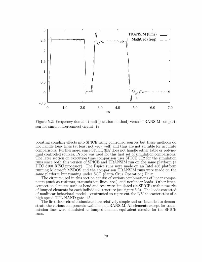
-0.5
0
0.5
1
1.5
2
2.5
3
0 1.0 2.0 3.0 4.0 5.0 6.0 7.0
TRANSIM (time)MathCad (freq)
ns
Figure 5.2: Frequency domain (multiplication method) versus TRANSIM compari-son for simple interconnect circuit, V2.
porating coupling effects into SPICE using controlled sources but these methods donot handle lossy lines (at least not very well) and thus are not suitable for accuratecomparisons. Furthermore, since SPICE 3E2 does not handle either table or polyno-mial controlled sources, Pspice was used for this first set of simulation comparisons.The later section on execution time comparison uses SPICE 3E2 for the simulationruns since both this version of SPICE and TRANSIM run on the same platform (aDEC 3100 RISC processor). The Pspice runs were made on an Intel 486 platformrunning Microsoft MSDOS and the comparison TRANSIM runs were made on thesame platform but running under SCO (Santa Cruz Operation) Unix.
The circuits used in this section consist of various combinations of linear compo-nents (such as resistors, transmission lines, etc.) and nonlinear loads. Other inter-connection elements such as bend and tees were simulated (in SPICE) with networksof lumped elements for each individual structure (see figure 5.3). The loads consistedof nonlinear behavioral models constructed to represent the I/V characteristics of ahigh speed TTL NAND gate [45].
The first three circuits simulated are relatively simple and are intended to demon-strate the various components available in TRANSIM. All elements except for trans-mission lines were simulated as lumped element equivalent circuits for the SPICEruns.
70

Figure 5.3: Lumped element models for microstrip bends and tees.
5.2.1 Single Microstrip Line
The microstrip lines used in all of the simulations was the same with dielectricconstant εr = 4.2, loss tangent td = 0.0001, height above the ground plane h =0.002mm, thickness of microstrip t = 0.0002mm and width w = 0.0023mm. Thepackaging parasitics for all runs consisted of an inductance L = 0.01nH and capac-itance C = 0.3pF [40]. The bends and other non-transmission line elements use themodels as shown in the example runsets of Appendix C.
Figure 5.4 shows a single microstrip line connected to a pulse source by way ofpackaging parasitic elements and a source resistor on one end and to a nonlinearmacromodel as described above on the other. Actually, the SPICE simulation usedthe standard ideal transmission line element since it has no provisions for specifyinga particular type of line. The resulting waveforms at the input (V1) and output (V3)of the line are shown in (a) and (b) respectively in figure 5.5. The pairs of waveformsare very similiar with difference due primarily because of SPICE’s limitations. Theideal line model used by this version of SPICE effects the delay down the line andthe simplified nonlinear load models required for SPICE effect the rise and fall times.
5.2.2 Microstrip with Lumped Elements
The next circuit demonstrates the lumped element ability of TRANSIM by usingfour microstrip lines along with a resistor, capacitor and inductor as shown in figure5.6. The lengths of the lines are as shown in the figure and the cross-section ofthe microstrip lines are given in section 5.2.1. The values for the lumped elementsare; R = 30Ω, L = 1nH and C = 1pF . The lines are of different lengths but thenonlinear loads are the same macromodels as used previously. The external portvoltages V1, V6 are shown in figure 5.7 (a) and (b) respectively and port voltagesV7, V9 are shown in figure 5.8 (c) and (d). Again, the pairs of waveforms are verysimiliar with differences due the effects noted in section 5.2.1.
71

Figure 5.4: Simple microstrip circuit.
5.2.3 Microstrip with Mutual Inductor
The third circuit shown in figure 5.9 shows the use of an ideal mutual inductor withexternal port voltages V1, V5 figure 5.10 (a) and (b) and V8 shown in figure 5.11(c). Note that an input pulse was only applied to the top line. The inductancesused for both the SPICE and TRANSIM runs were L1 = 1nH, L2 = 1nH and thecoupling coefficient was K = 0.99. The pairs of waveforms disagree more for thiscase than for previous test cases. It appears that the coupling is less pronouncedin the TRANSIM model than in the SPICE. No readily apparent bugs have beenfound in the TRANSIM mutual inductance model and therefore no real reason forthis difference has been found. Nevertheless, the sets of waveforms are still verysimiliar.
5.2.4 Microstrip Line with Bends
The circuit of figure 5.12 demonstrates a more complex circuit that uses microstriplines and bends along with nonlinear loads. As stated earlier, the SPICE version ofthis circuit uses lumped elements to model interconnection elements such as bends.The resulting waveforms at external ports V1 and V11 are shown in figure 5.13.
5.2.5 Clock Distribution Circuit
The final comparison circuit is a clock distribution network as shown in figure 5.14.The clock driver (U1) is shown driving a distribution network consisting of tworows of devices. Since SPICE can not directly handle coupled lines, coupling effectswere ignored. This circuit demonstrates microstrip tee and bend models along withthe planar transmission line and nonlinear loads. The output voltages for selectedexternal ports are shown in figure 5.15 (V1 and V8) and 5.16 (V42 and V83) for boththe SPICE and TRANSIM simulations. This circuit is also used as an examplenetlist in Appendix C.
72

-0.5
0
0.5
1
1.5
2
2.5
3
0 1 2 3 4 5 6 7
TRANSIMSPICE
ns (a)
-2
-1
0
1
2
3
4
5
6
7
0 1 2 3 4 5 6 7
SPICETRANSIM
ns (b)
Figure 5.5: SPICE and TRANSIM simulation of simple microstrip.
73

Figure 5.6: Demonstration circuit with microstrip lines and ideal lumped elements.
5.2.6 Accuracy Comparison Observations
It should be noted once again that all simulations were for lossless lines as theseversions of SPICE do not allow for lossy lines. Furthermore, SPICE (both 3E2 andPspice) had convergence problems on the more complicated circuits (particularlythe clock distribution example) and required several runs, tweaking some parame-ters (including subtle variations in line lengths) to obtain convergence. TRANSIMexperienced no convergence problems for any of the circuits.
As stated previously, the SPICE runs were performed under DOS using Pspicebecause of this versions enhanced ability to handle nonlinear behavioral models(by means of table and polynomial controlled sources). The TRANSIM runs wereperformed under UNIX but since they were on the same hardware platform (Intel486 based machine) the accuracies should be comparable. While this approach isuseful for waveform comparisons, it is not valid for execution time comparisons sincetwo different operating systems were used.
5.3 Timing Comparison Between SPICE and TRANSIM
To obtain execution time information between SPICE and TRANSIM, this same setof circuits were simulated using Berkeley’s SPICE 3E2 and TRANSIM running ona DEC 3100 RISC workstation with the Ultrix operating system.
A table showing the execution times for the various runs is shown in table 5.1.The three timing information columns show execution speed for SPICE 3E2, TRAN-SIM without thresholding, and TRANSIM with thresholding. Details about thethresholding concept can be found in previous chapters.
From these results, it is evident that TRANSIM is anywhere from 3 to 7 timesfaster than SPICE for the same circuit. Furthermore, because of it’s dependentsource limitations, the SPICE simulations used linear loads while the TRANSIMruns used table based behavioral models. Using more detailed SPICE load mod-els would probably have resulted in slower SPICE runs. Further improvements inTRANSIM processing speed are possible with the improvements discussed in Chap-ter 6. A detailed breakdown of execution time for the various main modules whichcomprise TRANSIM can be found in Chapter 5.
5.4 Coupled Lines
This set of simulations is intended to illustrate TRANSIM’s ability to handle cou-pled lines as well as the uncoupled ones often found in high density interconnection
74

-0.5
0
0.5
1
1.5
2
2.5
3
3.5
0 1e-09 2e-09 3e-09 4e-09 5e-09 6e-09 7e-09
SPICETRANSIM
V1
secs(a)
V
-1
0
1
2
3
4
5
0 1e-09 2e-09 3e-09 4e-09 5e-09 6e-09 7e-09
SPICETRANSIM
V6
secs(b)
V
Figure 5.7: Waveforms at ports 1 and 6 for microstrip with lumped elements.
75

-1.5
-1
-0.5
0
0.5
1
1.5
2
2.5
3
0 1e-09 2e-09 3e-09 4e-09 5e-09 6e-09 7e-09
SPICETRANSIM
V7
secs(c)
V
-2
-1.5
-1
-0.5
0
0.5
1
1.5
2
2.5
3
0 1e-09 2e-09 3e-09 4e-09 5e-09 6e-09 7e-09
SPICETRANSIM
V9
secs(d)
V
Figure 5.8: Waveforms at ports 7 and 9 for microstrip with lumped elements.
76

Figure 5.9: Demonstration circuit containing microstrip lines and mutual inductor.
Table 5.1: Comparison of execution times for SPICE 3e2 and TRANSIM. The driversand receivers were modeled as behavioral models in TRANSIM and as linear loadsin SPICE 3e2 since this type of nonlinear models are not supported.
Circuit Description SPICE TRANSIM TRANSIMFigure 3e2 No Threshold 95% Threshold
5.4 Microstrip 1.8s 16s 3s5.12 Microstrip 86.7s 23s 12s
w/bends5.9 Microstrip 43.8s 64s 28s
w/mut. ind.5.14 Clock 3637s 2219s 1369s
Distrib. (60.5min) (37min) (23min)
systems.The first simulation was of the coupled transmission line circuit pair illustrated in
figure 5.17. This circuit consists of two microstrip lines (width = 0.004 mm, heightabove ground plane = 0.002 mm, thickness = 0.0002 mm, dielectric constant = 4.2,separation = 0.002 mm, tand = 0.01) connected to nonlinear macromodeled loadsand driven by a pulse generated through a 50Ω source resistance. The pulse sourceis connected to the interconnection structure through the same parasitic packagingelements that are found in the nonlinear loads. These loads are the same fast TTLloads mentioned previously. The output waveforms are shown in figures 5.18 and5.19. Plot (a) shows the near end voltages (input pulse V1 and crosstalk noise V3).Plot (b) shows the far end signals (output pulse V2 and crosstalk noise V4). Plot (c)shows just the two crosstalk (victim line) signals.
As discussed in Appendix A, the calculations of admittance parameters for cou-pled lines involves finding the per unit length impedance, Z and admittance, Yparameters. This in turn requires knowledge of the per unit length inductance, Land capacitance, C matrices for the lossless case and in addition, the resistance,R and conductance, G matrices for the lossy case. For most lossy line situations,the dielectrics involved have a very low conductance resulting in vanishingly smalloff-diagonal values in the resistance matrix and a virtually zero conductance matrix.Therefore the conductance matrix is usually ignored and the resistance matrix istreated as being diagonal, composed of frequency dependent terms. For the cases
77

-1
-0.5
0
0.5
1
1.5
2
2.5
3
0 1e-09 2e-09 3e-09 4e-09 5e-09 6e-09 7e-09
SPICETRANSIM
V1
secs(a)
V
-2
-1
0
1
2
3
4
5
6
7
0 1e-09 2e-09 3e-09 4e-09 5e-09 6e-09 7e-09
SPICETRANSIM
V5
secs(b)
V
Figure 5.10: Waveforms at ports 1 and 5 for microstrip with mutual inductor.
78

-0.05
-0.04
-0.03
-0.02
-0.01
0
0.01
0.02
0.03
0.04
0 1e-09 2e-09 3e-09 4e-09 5e-09 6e-09 7e-09
SPICETRANSIM
V8
secs(c)
V
Figure 5.11: Waveforms at port 8 for microstrip with mutual inductor.
simulated here, identical conductors were assumed and therefore an explicit resis-tance matrix was not kept since all of the diagonal terms would be the same. Theresistance per unit length at each frequency was calculated and the same value usedfor each conductor.
The L and C matrices are frequency independent and need only be found once.Furthermore, the relationship between the L and C matrices is critical and thecalculation must be accurate. For the coupled line cases, the L and C matrices werecalculated using a separate set of programs developed by White and Nabors [47] forcalculating L and C matrices for complex 3D geometries. The inductance matriceswere calculated using FASTHENRY and the capacitance matrices using FASTCAP.The values for the two line case mentioned previously are shown in figure 5.20. Thefrequency dependent resistance was calculated using the standard skin effect modeldiscussed in [57].
The last coupled line example is shown in figure 5.21 which represents a sectionof data bus connecting two integrated circuits (represented by the sets of gates).For clarity, only the middle (vertical) group of lines were simulated as coupled lines.TRANSIM allows for multiple coupled line groups but the resulting waveforms be-come difficult to read and the final output is not intuitively obvious. In this example,the third line up from the bottom was driven by the same pulse source arrangementused in the other examples. Again, all loads and sources were connected to theinterconnection circuit by means of packaging parasitic elements. (The use of pack-
79

Figure 5.12: Demonstration circuit with microstrip lines and bends.
aging parasitics is not required but if they are not included then the FILTER optionmust be used in the netlist otherwise aliasing problems can arise during the FFTstage.) The cross-sectional measurements of the lines were the same as those usedabove and the line lengths are as marked in the figure. The resulting waveforms areillustrated in figures 5.22 and 5.23. Figure 5.22 (a) shows the near end signals forthe driven line and two of it’s nearest neighbors (V5, V3 and V1 respectively). Signalson victim lines further away from the driven line show virtually zero response (onthe order of a mV) and are not shown here. Figure 5.22 (b) shows the signals at thefar end including the output of the driven line and the two nearest victims (V6, V4
and V2 respectively). Figure 5.23 (c) shows just the near end victim line responsesand figure 5.23 (d) the far end response.
As mentioned in the discussion of the two coupled line simulation, the accuratecalculation of the L and C matrices is important and the same holds true for thecoupled line section of the data bus of figure 5.21. While very accurate (on the orderof 1% error), FASTCAP and FASTHENRY require significant computing resources(in terms of memory and cpu speed) and FASTCAP exceeded the limits of a SunMicrosystems SPARC10 RISC workstation with 240 megabytes of main memory and2 gigabytes of swap space. While remaining within the confines of computing envi-ronment, FASTHENRY was unable to converge to a solution on the same machineafter 96 hours. By using the nearest neighbor coupling approximation, it is possibleto obtain the full L and C matrices using the results of two coupled line calculations.
One method of arriving at the full L and C matrices without having to performcomputations on a nine conductor problem (eight data lines and the ground plane)is to collect data from a series of coupled line pairs and extrapolate these resultsinto full matrices.
Using this method, the results for each pair of adjacent lines would be the same(C11, C12, L11 and L12). The capacitances from a line to the next most adjacentline could be approximated by C13 = KC ′12 where C ′12 is the capacitance betweenthe first and third lines with the second removed. K is constant (K < 1) whosepurpose is to account for the field concentrating effects of the temporarily removed
80

-0.5
0
0.5
1
1.5
2
2.5
3
0 1e-09 2e-09 3e-09 4e-09 5e-09 6e-09 7e-09
V1SPICE
TRANSIM
secs
V
(a)
-2
-1
0
1
2
3
4
5
6
0 1e-09 2e-09 3e-09 4e-09 5e-09 6e-09 7e-09
SPICETRANSIM
V11
secs
V
(b)
Figure 5.13: Waveforms at ports 1 and 11 for microstrip with bends.
81

Figure 5.14: Clock distribution circuit.
intervening conductor(s). Initially a value of 1/2 was chosen, effectively dividing thedouble separation capacitance over the second and third conductors.
As noted previously, the relationship between L and C is important. Usingthis scheme and a similar one for the inductances resulted in a combination oftime domain admittance parameter impulse responses that produced meaninglessoutputs. Various values of K were examined all with similar results.
Therefore to simulate coupled line groupings greater than two, the nearest neigh-bor approximation was used. In this method, coupling is assumed to occur betweena line and its immediate neighbors and coupling between lines further removed isassumed to occur through each intervening line. The assumption is validated by itsuse in reducing coupling between data lines by inserting a grounded line in betweenthe pair of signal lines.
Using this assumption, the L and C matrix for the data bus example was builtup from the two coupled line case (the line geometries and spacings being the same).This results in tridiagonal matrices for L and C with the diagonal elements beingL11 and C11 respectively (L11 and C11 come from the two conductor case). Theupper and lower diagonal entries of L and C are L12 and C12 respectively.
5.5 Module Timing Breakdown of TRANSIM
TRANSIM is composed of a large number of modules but in general there are fivecomputationally intensive areas:
1. Build the complete nodal admittance matrix.
2. Reduce the NAM producing the RNA.
3. Augment the RNA with the augmentation network.
4. Convert y(f) to y(t) (including STSS error correction).
5. Perform the transient analysis.
82

-1.5
-1
-0.5
0
0.5
1
1.5
2
2.5
3
0 1e-09 2e-09 3e-09 4e-09 5e-09 6e-09 7e-09 8e-09 9e-09
SPICETRANSIM
V1
secs(a)
V
-1.5
-1
-0.5
0
0.5
1
1.5
2
2.5
3
0 1e-09 2e-09 3e-09 4e-09 5e-09 6e-09 7e-09 8e-09 9e-09
SPICETRANSIM
V8
secs(b)
V
Figure 5.15: Waveforms at ports 1 and 8 for clock distribution circuit.
83

-1.5
-1
-0.5
0
0.5
1
1.5
2
2.5
3
3.5
4
0 1e-09 2e-09 3e-09 4e-09 5e-09 6e-09 7e-09 8e-09 9e-09
SPICETRANSIM
V42
secs(c)
V
-1.5
-1
-0.5
0
0.5
1
1.5
2
2.5
3
3.5
0 1e-09 2e-09 3e-09 4e-09 5e-09 6e-09 7e-09 8e-09 9e-09
SPICETRANSIM
V83
secs(d)
V
Figure 5.16: Waveforms at ports 42 and 83 for clock distribution circuit.
84

Figure 5.17: Demonstration circuit for microstrip coupled lines.
A graph illustrating the average relative execution time for these areas is shownin figure 5.24. The execution times for the various major areas within TRANSIMwere computed and the results saved in a log file for each example circuit used in thischapter. A weighted average of these times was used to arrive at the percentagesdisplayed in the chart. The weighting factor used for each circuit was the number ofnonlinear external terminals. While somewhat arbitrary, this weighting factor givesa reasonable metric of the circuit’s complexity. The total number of terminals ineach circuit was used as the weighting factor.
The amount of time spent in each of these areas is highly dependent on the circuitbeing simulated. Circuits with a large total number of terminals but relatively fewexternal ones will spend a greater proportion of the total execution time in theNAM reduction phase than a circuit with an equivalent number of total nodes butmore external terminals. This is because the matrix reduction routines have feweroperations to perform since the amount of work to be done is directly related tothe difference between the total number of terminals and the number of externalones. For example, if a circuit has a total of M terminals and M − 2 of them areexternal, then only two rows and columns need be eliminated (from each floor inthe cityscape) from the NAM to arrive at the RNA. If, however, there are only twoexternal terminals then M − 2 rows and columns need to be eliminated resulting inlonger execution times in the reduction phase.
The percentage of execution time spent in each of the major areas of TRANSIMas revealed in figure 5.24 show some surprising and some not so surprising results.
The fact that the average FFT time occupied only 3.62% of the total executiontime is not surprising considering the efficient FFT algorithm used to perform thetransform.
One of the first surprises was how little time was spent in the build phase of theNAM. This only occupied an average of 3.75% of the total run time. This proportionremained relatively small even for circuits which contained computationally inten-sive models such as coupled lines. The save table concept and reuse of previouslycalculated parameters helps reduce the overall execution time significantly and fromthis chart it’s apparent that little improvement to the build stage is justified. Con-sequently this particular phase in program execution is not addressed in Chapter6.
The transient analysis time slice varied some depending on the complexity ofthe circuit but was mainly influenced by the number of external ports. This makessense in that the total number of time domain admittance parameters involved in the
85

-0.5
0
0.5
1
1.5
2
2.5
3
0 1e-09 2e-09 3e-09 4e-09 5e-09 6e-09 7e-09
V1V3
secs
V
(a)
-0.5
0
0.5
1
1.5
2
2.5
3
0 1e-09 2e-09 3e-09 4e-09 5e-09 6e-09 7e-09
V2V4
secs
V
(b)
Figure 5.18: Near and far end waveforms for coupled line pair.
86

-0.4
-0.3
-0.2
-0.1
0
0.1
0.2
0.3
0.4
0 1e-09 2e-09 3e-09 4e-09 5e-09 6e-09 7e-09
V3V4
secs(c)
V
Figure 5.19: Crosstalk waveforms for coupled line pair.
convolutions is equal to the square of the number of external ports. The topologyof the simulated circuit and the type of models used for individual elements also hasa pronounced effect on the transient execution time. In general, topologies with alarge number of coupled lines will have longer execution times than a circuit withthe equivalent number of internal and external terminals but few multiport devices.
Complex multiport devices tend to have complicated admittance responses re-sulting in relatively messy impulse responses with a large number of closely spacedbin groups. Thresholding can reduce the total number of bins used in the convo-lution stages but the effect will not be as pronounced. The number of bins for amicrostrip, for example, will go from say 2048 to less than 100 after thresholdingbut for the cross coupling admittance parameters in a coupled line (such as y14(t))the number of bins after thresholding may be on the order 700.
87

Figure 5.20: L and C matrices for two coupled microstrips.
Figure 5.21: Demonstration circuit, data bus.
88

-1
0
1
2
3
4
5
6
0 1e-09 2e-09 3e-09 4e-09 5e-09 6e-09 7e-09
V5V3V1
secs
V
(a)
-1
0
1
2
3
4
5
6
0 1e-09 2e-09 3e-09 4e-09 5e-09 6e-09 7e-09
V6V4V2
secs
V
(b)
Figure 5.22: Near (a) and far (b) end bus waveforms showing culprit and victimlines.
89

-0.2
-0.15
-0.1
-0.05
0
0.05
0.1
0.15
0.2
0 1e-09 2e-09 3e-09 4e-09 5e-09 6e-09 7e-09
V1V3
secs
V
(c)
-0.3
-0.2
-0.1
0
0.1
0.2
0.3
0 1e-09 2e-09 3e-09 4e-09 5e-09 6e-09 7e-09
V2V4
secs
V
(d)
Figure 5.23: Near (c) and far (d) end bus waveforms, victim lines only.
90

AAAAAAAAAAAAAAAAAAAAAAAAAAAAAAAAAAAAAAAAAAAAAAAAAAAAAAAAAAAAAAAAAAAAAAAAAAAA
AAAAAAAAAAAAAAAAAAAAAAAAAAAAAAAAAAAAAAAAAAAAAAAAAAAAAAAAAAAAAAAAAAAAAAAAAAAA
AAAAAAAAAAAAAAAAAAAAAAAAAAAAAAAAAAAAAAAAAAAAAAAAAAAAAAAAAAAAAAAAAAAAAAAAAAAA
AAAAAAAAAAAAAAAAAAAAAAAAAAAAAAAAAAAAAA
AAAAAAAAAAAAAAAAAAAAAAAAAAAAAAAAAAAAAAAAAAAAAAAAAAAAAAAAAAAAAAAAAAAAAAAAAAAAAAAA
AAAAAAAAAAAAAAAAAAAAAAAAAAAAAAAAAAAAAAAAAAAAAAAAAAAAAAAAAAAAAAAAAAAAAAAAAAAAAAAA
AAAAAAAAAAAAAAAAAAAAAAAAAAAAAAAAAAAAAAAAAAAAAAAAAAAAAAAAAAAAAAAAAAAAAAAAAAAAAAAA
AAAAAAAAAAAAAAAAAAAAAAAAAAAAAAAAAAAAAAAAAAAAAAAAAAAAAAAAAAAAAAAAAAAAAAAAAAAAAAAA
AAAAAAAAAAAAAAAAAAAAAAAAAAAAAAAAAAAAAAAA
AAAAAAAAAAAAAAAAAAAAAAAAAAAAAA
AAAAAAAAAAAAAAAAAAAAAAAAAAAAAAAAAAAAAAAAAAAA
AAAAAAAAAAAAAAAAAAAAAAAAAAAAAAAAAAAAAAAAAAAA
AAAAAAAAAAAAAAAAAAAAAAAAAAAAAAAAAAAAAAAAAAAA
AAAAAAAAAAAAAAAAAAAAAAAAAAAAAAAAAAAAAAAAAAAA
AAAAAAAAAAAAAAAAAAAAAAAAAAAAAAAAAAAAAAAAAAAA
AAAAAAAAAAAAAAAAAAAAAAAAAAAAAAAAAAAAAAAAAAAA
AAAAAAAAAAAAAAAAAAAAAAAAAAAAAAAAAAAAAAAAAAAA
AAAAAAAAAAAAAAAAAAAAAAAAAAAAAAAAAAAAAAAAAAAAAAAAAAAA
AAAAAAAAAAAAAAAAAAAAAAAAAAAAAAAAAAAAAAAAAAAAAAAAAAAA
AAAAAAAAAAAAAAAAAAAAAAAAAAAAAAAAAAAAAAAAAAAAAAAAAAAAAAAAAAAAAAAAAAAAAAAAAAAAAAAAAAAAAAAAAAAAAAAA
AAAAAAAAAAAAAAAAAAAAAAAAAAAAAAAAAAAAAAAAAAAAAAAAAAAAAAAAAAAAAAAAAAAAAAAAAAAAAAAAAAAAAAAAAAAAAAAA
AAAAAAAAAAAAAAAAAAAAAAAAAAAAAAAAAAAAAAAAAAAAAAAAAAAAAAAAAAAAAAAAAAAAAAAAAAAAAAAAAAAAAAAAAAAAAAAA
AAAAAAAAAAAAAAAAAAAAAAAAAAAAAAAAAAAAAAAAAAAAAAAAAAAAAAAAAAAAAAAAAAAAAAAAAAAAAAAAAAAAAAAAAAAAAAAA
AAAAAAAAAAAAAAAAAAAAAAAAAAAAAAAAAAAAAAAAAAAAAAAAAAAAAAAAAAAAAAAAAAAAAAAAAAAAAAAAAAAAAAAAAAAAAAAA
AAAAAAAAAAAAAAAAAAAAAAAAAAAAAAAAAAAAAAAAAAAAAAAAAAAAAAAAAAAAAAAAAAAAAAAAAAAAAAAAAAAAAAAAAAAAAAAA
AAAAAAAAAAAAAAAAAAAAAAAAAAAAAAAAAAAAAAAAAAAAAAAAAAAAAAAAAAAAAAAAAAAAAAAAAAAAAAAAAAAAAAAAAAAAAAAA
AAAAAAAAAAAAAAAAAAAAAAAAAAAAAAAAAAAAAAAAAAAAAAAAAAAAAAAAAAAAAAAAAAAAAAAA
AAAAAAAAAAAAAAAAAAAAAAAAAAAAAAAAAAAAAAAAAAAAAAAAAAAAAAAA
AAAAAAAAAAAAAAAAAAAAAAAAAAAAAAAAAAAAAAAAAAAAAAAAAAAAAAAA
AAAAAAAAAAAAAAAAAAAAAAAAAAAAAAAAAAAAAAAAAAAAAAAAAAAAAAAA
AAAAAAAAAAAAAAAAAAAAAAAAAAAAAAAAAAAAAAAAAAAAAAAAAAAAAAAA
AAAAAAAAAAAAAAAAAAAAAAAAAAAAAAAAAAAAAAAAAAAAAAAAAAAAAAAA
AAAAAAAAAAAAAAAAAAAAAAAAAAAAAAAAAAAAAAAAAAAAAAAAAAAAAAAA
AAAAAAAAAAAAAAAAAAAAAAAAAAAAAAAAAAAAAAAAAAAAAAAAAAAAAAAA
AAAAAAAAAAAAAAAAAAAAAAAAAAAAAAAAAAAAAAAAAAAAAAAAAAAA
AAAAAAAAAAAAAAAAAAAAAAAAAAAAAAAAAAAAAAAAAAAAAAAAAAAA
AAAAAAAAAAAAAAAAAAAAAAAAAAAAAAAAAAAAAAAAAAAAAAAAAAAA
AAAAAAAAAAAAAAAAAAAAAAAAAAAAAAAAAAAAAAAAAAAAAAAAAAAA
AAAAAAAAAAAAAAAAAAAAAAAAAAAAAAAAAAAAAAA
AAAAAAAAAAAAAAAAAAAAAAAAAAAAAAAAAAAAAAAAAAAAAAAAAAAAAAAAAAAAAAAAAAAAAAAAAAAAAAAAAAAAAAAAAAAAAAAA
AAAAAAAAAAAAAAAAAAAAAAAAAAAAAAAAAAAAAAAAAAAAAAAAAAAAAAAAAAAAAAAAAAAAAAAAAAAAAAAAAAAAAAAAAAAAAAAA
AAAAAAAAAAAAAAAAAAAAAAAAAAAAAAAAAAAAAAAAAAAAAAAAAAAAAAAAAAAAAAAAAAAAAAAAAAAAAAAAAAAAAAAAAAAAAAAA
AAAAAAAAAAAAAAAAAAAAAAAAAAAAAAAAAAAAAAAAAAAAAAAAAAAAAAAAAAAAAAAAAAAAAAAAAAAAAAAAAAAAAAAAAAAAAAAA
AAAAAAAAAAAAAAAAAAAAAAAAAAAAAAAAAAAAAAAAAAAAAAAAAAAAAAAAAAAAAAAAAAAAAAAAAAAAAAAAAAAAAAAAAAAAAAAA
AAAAAAAAAAAAAAAAAAAAAAAAAAAAAAAAAAAAAAAAAAAAAAAAAAAAAAAAAAAAAAAAAAAAAAAAAAAAAAAAAAAAAAAAAAAAAAAA
AAAAAAAAAAAAAAAAAAAAAAAAAAAAAAAAAAAAAAAAAAAAAAAAAAAAAAAAAAAAAAAAAAAAAAAAAAAAAAAAAAAAAAAAAAAAAAAA
AAAAAAAAAAAAAAAAAAAAAAAAAAAAAAAAAAAAAAAAAAAAAAAAAAAAAAAAAAAAAAAAAAAAAAAAAAAAAAAAAAAAAAAAAAAAAAAA
Breakdown of TRANSIM Execution Time
3.74%
38.00%
14.43%3.62%
40.21%
BuildTransient
Reduce
AugmentFFT
Figure 5.24: TRANSIM execution time statistics.
91

Chapter 6
TRANSIM Improvements
6.1 NAM Reduction Improvements
There are a number of ways to improve on this matrix reduction method that utilizethe unique nature of the linear, reciprocal devices used in its construction. Theseimprovements fall into two categories; memory usage minimization and speed en-hancements.
6.1.1 Memory Enhancements
When dealing with complex circuits, it is inevitable that a large amount of datawill be created. Requiring or assuming an unlimited supply of main memory isimpractical and even a large memory array will eventually prove insufficient for asignificantly large circuit (like closet space in a house). Once the data arrays growlarge enough, the system will of necessity have to swap blocks of data to the swapspace on a (usually) slower device, often a harddisk. Rather then let the systemperform this function in what may be an inefficient method (as far as the simulatoris concerned), the program should perform this swapping itself.
The simplest way to handle this problem with the NAM involved in the reductionprocess also applies to other portions of the simulator that deal with the NAM (suchas the Build stage). Most operations on the NAM are at the floor level (includingthe reduction process) and the only step that uses an entire tower at once is theFFT stage. Therefore, rather than deal with the entire sparse NAM (or cityscape)at once, subgroups of floors can be handled instead. The number of floors in afloor group depends on two factors; the amount of available main memory and theextent of the street plan (the total number of internal and external nodes in thecircuit). The worst case scenario is if all the nodes in a circuit were connected tosome huge multiport device. In this case the floor plan would be completely filledwith no vacancies. On the other hand, this would also imply that all of the nodeswere external and thus no reduction would be required in the first place.
In general, the number of entries on one floor of the initial NAM can be foundfrom the following expression
NF = 3NI + 2NE +P∑j=1
(MPj−2 )MPj (6.1)
where NI is the number of internal nodes, NE is the number of external nodes,MPj is the number of ports in multiport j and P is the number of multiports. Themeaning of these variables is best illustrated with an example (see figure 6.1).
Consider the example in figure 6.1. Here there are five uncoupled lines connectingterminal pairs (2,3), (3,4), (6,7), (9,10) and (10,11). These are 2-port devices andare not considered multiports according to this method. Only structures with morethan two ports will be considered multiports. Thus this example has two multiport
92

devices represented by the pairs of coupled linesM1 and M2. An internal terminal isany terminal which is not connected to an external load (i.e. any terminal for whichvoltage and current values are being calculated). By definition, internal terminalsmust have more than one connection; each terminal must have a feed connection anda drain connection. Thus an internal terminal sees its’ self admittance along withthe mutual admittance’s looking down the feed and drain connections. In the NAMthis means that there are three entries in each row corresponding to an internalnode. This fact is indicated in (6.1) by the 3NI term. External nodes have onlydrain lines (as far as the linear NAM is concerned) and thus any external node seesonly its self admittance and one mutual admittance (looking down the drain line).This results in the 2NE term in the equation.
Figure 6.1: Floor plan of multiport interconnect example.
Each multiport device reflects the cross coupling terms between nets of 2 portdevices. A multiport could be a set of coupled lines or some device like a multitap“tee”such as that in figure 6.2 (a). The number of additional entries to the NAM(on each floor) can be found by examining an N-port device represented by a set ofN/2 coupled lines ((b), figure 6.2). At any port k, there is the self admittance atthat port (ykk). By convention, each port can be thought of as being connected toone other port as a through admittance (ykl) and to all other ports by the remainderof the multiport. This is an artificial distinction but it makes the calculation of thenumber of entries in the NAM much easier. This separation is necessary since thefirst set of entry calculations assumed that all of the nodes were connected by 2-portdevices. If the proceeding distinction were not applied, there would be duplicationin the entry count.
Standing at one port of the multiport device, one sees through admittance’s toeach of the other ports. Since the self admittance and one through admittance havealready been accounted for, this means that there are MP − 2 through admittancesas seen from the current port. Repeating this process for the other ports, we seethat the total number of through admittance’s is (MP − 2)MP . There can be morethan one multiport device in a circuit so if we assume that there are P multiports
93

Figure 6.2: Multiport device examples.
each with a different number of ports (MPj , j = 1 . . . P ) then the total number of
entries due to multiports is∑Pj=1(MPj−2)MPj , which is the last term in (6.1).
The total memory used by the initial NAM is then
memory usage = NF · 2 ·Nfreq ·Ndouble (6.2)
where NF is the number of entries per floor, Nfreq is the number of frequencies (num-ber of floors)and Ndouble is the number of bytes used per double precision number(machine dependent). The factor of 2 is because the data is complex, requiring twodoubles for each data point.
After the circuit netlist is processed, there is sufficient information that the re-quired memory to build the NAM could be found. If this amount is greater thansome preset limit (based on some function of system resources) then the build andreduction processes must be performed in floor groups. Note that both of these pro-cesses are dependent only on values at a specific frequency and not on values fromother floors. Therefore processing could proceed on a floor by floor basis with theresults appended to a temporary file on the disk. If the circuit file is very large, thismay be required but in general the disk I/O’s should be performed as infrequentlyas possible. Many of the routines for calculating admittance values for a given el-ement are vectorized with respect to frequency. Thus all of the admittances for allfrequencies are calculated in one shot which does not fit into this new memory man-agement strategy. The modifications to these routines is straightforward. Initially,TRANSIM generates a frequency vector that contains all of the frequencies at whichadmittance values will be calculated. A vector is used rather than using start, stopand step variables because table based models may not have information collected atevenly spaced frequencies. The vectorized device routines need the addition of startand stop frequencies passed to them along with the frequency vector. Frequencyindependent data for each device type needs to be kept between processing of floorgroup calls. Currently each call to the vectorized routines requires recalculation offrequency independent parameters (like capacitance in some models). This is notan extremely critical issue if the number of group calls is small since recalculationwould occur only once for each call.
94

6.1.2 Other Matrix Reduction Memory Enhancements
Each cycle in the matrix reduction routine eliminates one row and column of a floorin the NAM. As noted earlier, each cycle can also contribute to filling of the originalsparse matrix. Therefore the total memory used in the current method rises asthe reduction proceeds even though whole rows and columns are being eliminated(actually the values in those locations are being set to zero, the memory is still inuse).
Modifying the reduction cycle to free these eliminated rows and columns aftereach pass would save some memory but would require changing the structure ofthe 3D sparse matrix. Remember that the NAM is based on a city block schemewith towers erected for each admittance parameter. Unfortunately, matrix reductionhas to occur floor by floor and freeing part of each building after each cycle is notpossible. Furthermore, the gain in memory would be offset by the longer executiontime required to perform the memory deallocation schemes.
A better method is to use a few less floors in each floor group and let the memoryrequirements fluctuate as necessary.
6.1.3 Speed Enhancements to Matrix Reduction
As mentioned in the description of the matrix reduction algorithm, the reductionis performed on each element of the entire matrix without regard to its sparsenessor symmetry. The only concession to the general case is that only the diagonal issearched for pivots (unless no pivot greater than some minimum amount is found,then off diagonal pivots are looked at). Consider for a moment the floor plan shownin figure 6.3. This represents the last stage of a cycle in the matrix reduction justprior to the row subtraction operations. The last row is divided by AMM (the pivot)and the following operation is performed at each row k (M = 5 in this example)
Akj = Akj −AMjAkM (6.3)
Figure 6.3: Last floor plan in NAM reduction cycle.
The last term in the equation represents entries in the M th column. If that entryis zero, then the processed row is unaffected and remains the same. In the currentmethod, M−1 divisions, M multiplication’s and M subtraction’s are still performedexcept that zero is subtracted from each element of the current row.
This leads to the first speed enhancement to the matrix reduction algorithm. Byscanning down the M th (last) column, only rows with a non zero entry should be
95

processed. If the M th column contains zero or is an unallocated tower, then that rowshould be left alone. The last row should not be processed at all since it becomesall zeros in the end anyway.
Further speedups could be accomplished by checking which elements in the lastrow have non zero elements and only perform subtraction’s on the elements of targetrows that have non zero values in the same column. This would not save much inexecution time if comparisons were made at each point to determine if a subtractionshould occur. Since the matrix is symmetric about the diagonal, (again assumingreciprocal interconnect elements) finding the non zero elements in the M th columnsimultaneously finds the non zero elements in the M th row. This information couldbe used to form an integer vector whose elements are the locations of the non zerocomponents. This combined with the total number of non zero elements can be usedas the indexing for the row subtraction cycle. A block diagram of this new algorithmis shown in figure 6.4. This diagram illustrates the reduction of an M ×M matrixby one row and column. Note that the M th row has already been normalized by thepivot value before beginning this algorithm.
Figure 6.4: Purposed improved NAM reduction algorithm.
An example best illustrates the time saved by this new algorithm. Figure 6.5 is asimple interconnection structure with five transmission lines, a tee and a bend. Forthe original method there were M − 1 = 8 rows processed (M = 9, the number ofterminals in the entire circuit). Since there are M multiples (×) and M additions(+) per row in the old method there are (M − 1)M = 72 multiplies and (M −1)M = 72 additions involved to perform the old reduction. For the new method,there are only 3 rows processed with 3 multiply and 3 addition operations per row.For this particular example there are approximately 88% fewer operations with thenew method than with the current one (this reduction is for both multiplies andadditions).
96

Figure 6.5: New NAM reduction example circuit
6.1.4 New NAM Storage Methodology
As in most simulation work, there is a tradeoff between speed and memory require-ments. In the simplest sense, main memory use can be kept to almost nothing ifone is willing to use the system mass storage (such as a hard disk subsystem) asvirtual memory. Obviously this is totally unacceptable for a practical simulator. Ifmemory use were the only consideration in TRANSIM, then the NAM build andreduction processes would be combined and the construction of the sparse city mapand consequent fill problems would be avoided. Since each floor represents a uniquefrequency and the stored data (admittance’s) are independent of past or future fre-quencies (assuming a linear medium and devices), then each floor can be completelyprocessed before the next floor is constructed.
The final result of the combined build/reduce process would be a dense towerstructure. Thus space would only need to be allocated once with the total numberof towers being M ×M , where M is the number of external nodes in the circuit.
The problem with this method is the significant amount of recalculation thatmust be done at each frequency if total NA processing is done on a floor by floor basis.The frequency independent intermediate terms used in calculating the admittance’sfor many of the interconnection elements would have to be recalculated at each floorwhereas the current method performs this admittance calculation in a vectorizedform to eliminate these redundant calculations.
This is significant in complex circuits with a large number of different elements.In a circuit with a large number of similar elements, the advantage to the vector-ized routines may be less important because of the reuse of data from previouslyencountered elements. For example, if a bend with the same physical characteristicsis encountered hundreds of times, only the first encounter will required admittancecalculations. Subsequent encounters will not require any admittance calculations.Since the vectorization is only helpful on the first encounter, the speed advantagesof this vectorization may be out weighed by the memory saving of single shot floorprocessing.
It is most likely that this later type of circuit will be encountered most oftensince most physical packaging methods allow for relatively few unique element typesbut there are a lot of them in a particular design. A routing system may only allow90 deg bends in its layouts but hundreds or thousands may be used in a particulardesign.
6.2 NAM Augmentation by Matching Network
The current method of augmenting the original nodal admittance matrix is to per-form a set of matrix operations to add in the effects of the two matching resistance’s
97

(the linear half the matching network). If Y is the original nodal admittance matrix,then the augmented nodal admittance matrix is
Y ′ = [Y −1 − I · Zm]−1 + I · 1
Zm(6.4)
Note that this method requires two matrix inversions to augment the originalNAM. Since the NAM is actually a 3D matrix of Nf 2D matrices each of size MxM(Nf is the number of frequency points used), this can result in a large numberof inversions of some relative large matrices. From the statistics collected fromrunning the simulations reported in the Results section (Chapter 5) this counts forapproximately 14execution time.
The individual device models return admittance parameters for each of the se-lected frequencies and these are used to build the NAM. These same models couldeasily return impedance parameters and a nodal impedance matrix (NZM) con-structed instead. This NZM could then be augmented directly by the first matchingresistance and the final augmented admittance matrix would only require one matrixinversion as shown in 6.5.
Y ′ = [Z − I · Zm]−1 + I · 1
Zm(6.5)
Since the majority of the time spent in augmenting the original NAM is used inperforming the inversions, eliminating half of them should result in a 7% reductionin overall execution time.
Using an initial impedance matrix would require modifying the device models(for nodes and NCG this should be a simple operation) and the admittance matrixbuild module (which would now become a impedance build module). While the laststep is not as simple as modifying the models, it is still a relatively straightforwardproblem.
6.2.1 Uses of Symmetry
Most linear interconnection devices are inherently symmetric in nature, especiallythose used in structures for which TRANSIM was intended. Granted there are someinterconnection elements that are non symmetrical but TRANSIM was never in-tended to handle these types of devices. Currently little use is made of the symmetricnature of the individual elements found in an interconnection system by TRANSIM.Using the symmetric properties of these devices can be used in the following areasto reduce memory usage and speed up computation. Some of the improvements arealmost trivial in nature, others will require significantly more work but none shouldrequire an inordinate amount.
• Save-Table Memory Use Reduction:Currently the Save Table system works to reduce the amount of recalculationrequired when the same device is repeatedly encountered in an interconnectionsystem. For nodes this means a M×N×N 3D Y (f) matrix is stored where Mis the number of frequencies and N is the number of ports used by the node.If symmetry is assumed, then the only values that need to be stored are those
98

above and including the diagonal elements. This would result in a savings ofK locations per floor where K is
K = N2 − N(N + 1)
2(6.6)
For example, a 3-port device (such as a tee) with y parameters calculated for1024 frequencies, the savings would be[
32 − 3 · 22
]× 2× 4× 1024 = 49152 (6.7)
or approximately 50kb of memory. The factor of 2 is because the y parametersare complex and the factor of 4 accounts for the number of bytes needed torepresent the real and imaginary parts of each number.
• NAM Memory Use Reduction:The same sorts of symmetry arguments can be used to establish a new sparsematrix storage technique for the complete nodal admittance matrix. Since eachindividual device used in making up the NAM is assumed to be symmetric,then the complete NAM is also symmetric and the amount of memory requiredto store the NAM drops by approximately 40
• NAM Augmentation Speed EnhancementThe current method for augmenting the NAM involved two 3D matrix in-versions which together account for (on average) 14mentioned above, one ofmatrix inversions could be eliminated but this would require either rewritingthe individual device models to return impedance (Z) matrices instead of Yor rewriting other parts of the simulator such that the primary matrix is acomplex nodal impedance matrix (NZM). Both techniques requiring rewritingvarious modules scattered throughout the code. An alternative would be toeliminate the general purpose matrix inversion code currently in use and derivea specialized inversion module that is specifically designed to take advantageof the symmetries involved. Further research would be required to find and/ordevelop such a function but considering that brute force matrix inversion isone of the most computationally intensive mathematical operations, any othertechnique would certainly result in a speed enhancement.
• NAM Reduction Speed EnhancementTechniques for improving the NAM reduction have been mentioned above andinclude discussions on the use of symmetry to improve over the relatively simplerow/column operations currently in use.
• FFT and STSS Error Correction Speed EnhancementIf the NAM storage is designed to take advantage of symmetry, then this sav-ings will be passed into the frequency to time domain conversion and STSSerror correction as a reduction in processing time (with the appropriate but mi-nor changes to these algorithms). Currently all of the elements in the RNAMare converted to their time domain counterparts and each is thresholded andcorrected by the STSS method. Since the frequency domain RNAM is sym-metric (it can be shown that if the NAM is symmetric then the RNAM isalso) there are N2 − N(N + 1)/2 unnecessary FFT’s (and error corrections)performed.
99

• Time Domain Admittance Memory Use ReductionIf symmetry is used in the NAM and RNAM frequency domain matrices, thenit is obvious that the same symmetry should be used for the time domain Ymatrix storage, resulting in further memory savings.
6.3 Threshold Level Assignments
Currently TRANSIM allows the user to assign two relative threshold values; one forthe through terms in the admittance parameters and one for the cross coupling terms.For example, assume that a circuit consists of just a pair of coupled lines (like figure5.17). The threshold applied to the through terms (y11(t),y12(t), y21(t),y22(t),etc.) isdifferent from that applied to the cross terms (y13(t),y14(t), etc.). This is because theimpulse responses of the through terms consists of a few small bin groups whereasthe cross terms are significantly more detailed in structure with a larger number ofbin groups and with more bins in each such group. By having two different thresholdlevels, the level used for the through terms can be set lower, capturing more detailaround the bin groups but not seriously increasing the total number of bins capturedfor use in the transient analysis. A higher relative level can be used for the crossterms, resulting in some loss of detail but keeping the number of bins in the finalimpulse response relatively small.
This two part thresholding method could be improved, perhaps by relating thetwo levels and using the peaks of the through responses compared to the cross termsto determine both levels.
The reason for using coupled line models in an interconnection simulation shouldalso be evaluated further. The primary purpose for most designers is to estimatepotential problems due to glitches caused by crosstalk. In this situation, the peakheight of the glitch and it’s total energy are important considerations but otherfactors such as the duration of ringing at the beginning and end of the glitch aremuch less important. Therefore more severe thresholding can be performed on thecross terms which would result in a loss of detail but would also significantly decreaseexecution time.
6.4 Reuse of Time Domain NAM
Saving the time domain impulse response vectors (yij(t)) prior to thresholding anderror correction would allow for relatively fast multiple simulations using differentthresholding levels.
An option in the netlist could be used to tell the simulator when to look for anexisting Y (t) matrix (stored as a file) and use this data rather than recalculating allof the intermediate data. This would eliminate the building of the subNAM’s, thereduction of the full NAM and the augmentation of the reduced NAM. Since theseoperations can account for 50% of the total execution time, significant flexibilitymay be obtained by this option.
Alternately, information about the netlist (such as line lengths) could be storedwith Y (t). By comparing key information about the current netlist and the saveddata, a decision can be made as to the necessity of recalculating the frequencydomain NAM or reusing existing data.
The addition of this option would allow for initially high threshold values to beused, resulting in a rough approximation of the circuits performance. Additional
100

more accurate (and slower) simulations can be performed using lower thresholdinglevels if deemed necessary.
101

Chapter 7
Conclusions
7.1 Summary of Research and Original Contributions
The goal of this research was to develop a method of simulating the complex inter-connection systems found in high speed digital systems. Speed and realism were thetwo primary and often conflicting goals of the research. Many simulation methods(such as AWE) achieve their speed by abstracting the problem to a simplistic modelof the real world phenomenon. While useful for many problems, more accurate orat least more realistic models and methods are desired if only as a sanity check onthe simplified models.
As a means of demonstrating the concepts and original contributions producedduring the course of this research work, the simulator TRANSIM was created. Thetwo original goals of speed and realism lead to inclusion in the initial design ofself limiting admittance parameters and the thresholding concept (both originalcontributions).
Other original contribution occurred as work progressed in implementing thesetwo original goals. For example, new sparse matrix techniques were developed tolimit the amount of memory used for storage of the nodal admittance matrix. Savetables and the reuse of calculated parameters was developed to further save compu-tation time. Development of this concept also lead to the development of the matrixtechniques used for finding coupled and uncoupled line admittance parameters fromstored, length independent data (another original contribution).
While thresholding was one of the original ideas before implementation began,an acceptable method for dealing with the errors introduced by thresholding was notdiscovered until late in TRANSIM’s development. The STSS method is perhaps themost significant original contribution of this research because it allows relatively largethresholding levels to be used while dramatically reducing the errors introduced. Theneed for such a method was anticipated from the beginning but the amount of errorintroduced by even small thresholding levels was not expected and the original errorcorrection method proved inadequate.
In the effort to maintain realism, the incorporation of packaging parasitics toprovide naturally bandlimited admittance parameter responses lead to the intro-duction of a new matching network (another original contribution). The new dualmatching network (required to reduced impulse response lengths for low loss lines)was incorporated in TRANSIM from the beginning.
7.2 Future Goals
The difficulty in simulating complex interconnections structures is due primarilyto increasing clock speeds and wiring densities. With increasingly complex singlechip CPU’s, wider data paths and more complex architectures (such as massivelyparallel machines) better tools are needed by designers to analyze their designs priorto fabrication. Interconnection methods capable of meeting these requirements may
102

be relatively inexpensive to fabricate in quantity but the initial production cost ishigh, virtually precluding the building of prototypes.
Philosophically, a couple of conclusions have been reached as a result of perform-ing the research required to develop TRANSIM and the extensive literature reviewdone before, during and after the work was completed. First, trying to develop asimulator capable of extremely fast and accurate simulation of large interconnectionsystems is an illusive goal that will probably never be attained. Furthermore, toomuch emphasis has been placed on developing single element models (such as a setof coupled lines) with little thought as to the final use of such models.
What needs to be done? For one, the “do everything” simulator should be aban-don in favor of an integrated multifront approach. Since the interconnection struc-ture is a distributed element, any models developed for individual elements shouldbe based on that fact. Such models would ideally be based in the frequency domainto properly handle frequency dependent properties of transmission line structuresand materials.
The results of these models should then be used for performing either a fastbut less accurate simulation of a large portion of the interconnection system or in aslower but more accurate simulation of a much smaller subset of the total system.Depending on the users needs, both fast but less accurate large scale and slow,accurate small scale simulations are valid.
For fast but coarse simulations the detailed model information can be reducedand the resulting circuit simulated using something along the lines of the asymptoticwaveform evaluation method. While useful for examining timing effects, short termeffects such as glitches are of dubious value because of the use of reduced complexitymodels.
By developing a common set of calculated parameters for use by both types ofsimulation, model development time can be reduced and a common database fortable based models reused.
TRANSIM falls in the second ‘accuracy’ category but has some elements of thefirst in its use of thresholding. If the improvements discussed in chapter 6 areimplemented, execution time for complex circuits should decrease significantly (onthe order of 25% to 50%). Furthermore, as mentioned in chapter 6, performing anew transient analysis with previously calculated Y (t) data would result in fasterand more flexible simulations by skipping the build and reduction stages.
TRANSIM embodies the philosophical idea of a ‘complete’ interconnect simulatorin that it can handle the entire problem and is not just another single element modeldesigned to run (after a fashion) under SPICE. It provides accurate results fasterthan general purpose circuit simulators like SPICE and easily accepts new elementmodels. TRANSIM incorporates many novel circuit simulation concepts to obtainthis combination of speed and accuracy.
Further development, mostly incorporating existing CAD technology for matrixmanipulation as discussed in Chapter 6, will result in drammatic reductions in in-terconnect circuit simulation times.
103

References
[1] J.E. Schutt–Aine, R. Mittra, “Analysis of pulse propagation in coupled trans-mission lines,” IEEE Trans. on Circuits and Systems, Dec. 1985, pp. 1214–1219.
[2] N. Orhanovic, V.K. Tripathi, “Nonlinear transient analysis of coupled RLGClines by the method of characteristics,” Int. Journal of Microwave andMillimeter–Wave CAE, Vol. 2, No. 2, pp. 108–115.
[3] J.R. Griffith, M.S. Nakhla, “Time–Domain analysis of lossy coupled transmis-sion lines,”IEEE Trans. on Circuits and Systems, Oct. 1990, pp. 1480–1487.
[4] J.E. Schutt–Aine, R. Mittra, “Scattering parameter transient analysis of trans-mission lines loaded with nonlinear terminations,”IEEE Trans. on MicrowaveTheory and Techniques, Mar. 1988, pp. 529–536.
[5] F.Chang, “The generalized method of characteristics for waveform relaxationanalysis of lossy coupled transmission lines,”IEEE Trans. on Microwave The-ory and Techniques, Dec. 1989, pp. 2028–2038.
[6] F. Chang, “Relaxation simulation of transverse electromagnetic wave propa-gation in coupled transmission lines,”IEEE Trans. on Circuits and Systems,Aug. 1991, pp. 916–936.
[7] F. Chang, “Waveform relaxation analysis of RLCG transmission lines,”IEEETrans. on Circuits and Systems, Nov. 1990, pp. 1394–1415.
[8] R.E. Collins, Foundations for Microwave Engineering, McGraw–Hill, 1966,sections 4.7–4.9.
[9] C.W. Davidson, Transmission Lines for Communications, Macmillan Press,1978.
[10] J.D. Kraus and K.R. Carver, Electromagnetics, McGraw– Hill, 1973, chap. 13.
[11] R.A. Roberts and C.T. Mullis, Digital Signal Processing, Addison–Wesley Pub-lishing Co., 1987, p. 180–182
[12] T. Komuro, “Time–Domain analysis of lossy transmission lines with arbitraryterminal networks,” IEEE Trans. on Circuits and Systems, Oct. 1991, pp.1160–1164.
[13] Z. Ning, P.M. Dewilde, F.L. Neerhoff, “Capacitance coefficients for VLSI mul-tilevel metallization lines,” IEEE Trans. on Electron Devices, Mar. 1987, pp.644– 649.
[14] B. Easter, “The equivalent circuit of some microstrip discontinuities,”IEEETrans. on Microwave Theory and Techniques, Aug. 1975, pp. 655–660.
104

[15] A.F. Thomson, A. Gopinath, “Calculation of microstrip discontinuity induc-tances,”IEEE Trans. on Microwave Theory and Techniques, Aug 1975, pp.648– 655.
[16] C. Wei, R.F. Harrington, J.R. Mautz, T.K. Sarkar, “Multiconductor transmis-sion lines in multilayered dielectric media,”IEEE Trans. on Microwave Theoryand Techniques, Apr 1984, pp. 439–449.
[17] W. Ho, A.E. Ruehli, P.A. Brennan, “The modified nodal approach to networkanalysis,”IEEE Trans. on Circuits and Systems, Jun. 1975, pp. 504–509.
[18] J. Vlach, K. Singhal, Computer Methods for Circuit Analysis and Design, VanNostrand Reinhold, 1983.
[19] J. Vlach, K. Singhal, M. Nakhla, “Absolutely stable, high order method fortime domain solution of networks,”Arch. Elek. Ubertragung., vol. 30, pp. 157–166.
[20] F.H. Branin, “Transient analysis of lossless transmission lines,”Proc. IEEE,Nov. 1967, pp. 2012– 2013.
[21] C.W. Ho, “Theory and computer–aided analysis of lossless transmissionlines,”IBM J. Res. Develop., 17, 1973, pp. 249–255.
[22] D.S. Yaney, J.T. Nelson, L.L. Vanskike, “Alpha–particle tracks in silicon andtheir effect on dynamic MOS RAM reliability,”IEEE Trans. Electron Devices,Jan. 1979, pp. 10–16.
[23] R.F. Brown, “Model stability in use of moments to estimate pulse transferfunctions,” Electron. Lett., Vol. 7, Sept. 1971, pp. 587–589.
[24] M.F. Hutton and B. Friedland, “Routh approximations for reducing order oflinear, time–invariant systems,”IEEE Trans. Autom. Contr., Vol. AC–20, June1975, pp. 329–337.
[25] Y. Shamash, “Stable reduced–order models using Pade’ type approximations,”IEEE Trans. Autom. Contr., Vol. AC–19, Oct. 1974, pp. 615–616.
[26] Y. Shamash, “Failure of the Routh–Hurwitz method of reduction,” IEEETrans. Autom. Contr., Vol AC–25, Apr. 1980, pp. 313–314.
[27] Y. Shamash, “Truncation method of reduction: A viable alternative,” Elec-tron. Lett., Vol. 17, Jan. 1981, pp. 79–98.
[28] W.C. Elmore, “The transient response of damped linear networks with partic-ular regard to wideband amplifiers,” J. Appl. Phys., Vol. 19, 1948, pp. 55–63.
[29] M.M. Alaybeyi, J.Y. Lee, and R.A. Rohrer, “Numerical integration algo-rithms and asymptotic waveform evaluation (AWE),“ in IEEE Int. Conf. onComputer–Aided Design, 1992, p. 341.
105

[30] H. Heeb and A. Ruehli, “Retarded models for PC board interconnects —- orhow the speed of light affects your spice simulation,” in IEEE Int. Conf. onComputer–Aided Design, 1991, pp. 70–73.
[31] L.T. Pillage and R.A. Rohrer, “Asymptotic waveform evaluation for timinganalysis,” IEEE Trans. Computer–Aided Design of Integrated Circuits andSystems, Vol. 9, April 1990, pp. 352–366.
[32] C.L. Ratzlaff and N. Gopal, “RICE: rapid interconnect circuit evaluator,” inProc. 29 th ACM/IEEE Design Automation Conference, 1991, pp. 555–560.
[33] E. Chiprout and M. Nakhla, “Optimal pole selection in asymptotic waveformevaluation,” IEEE International Symposium on Circuits and Systems, May1992, pp. 1961–1964.
[34] R. Goering, “Startup’s simulator a challenge to SPICE,” Electronic Engineer-ing Times, Mar. 1, 1993, pp.23–24.
[35] L.J. Curran, “ ’A’ for effort,” IEEE Spectrum, Feb. 1993, pp. 50–52.
[36] Mark S. Basel , Michael B. Steer, Paul D. Franzon, and Dan Winkelstein,“High speed digital system simulation using frequency dependent transmissionline network modeling,” in IEEE MTT–S International Microwave SymposiumDigest, 1991, pp. 987–990.
[37] H. Riedell, M. Kay, M. Steer, J. Kasten, M. Basel, and R. Pomerleau, “Dielec-tric characterization of printed circuit substrates,” IEEE Proceedings, 1989,pp. 1–5.
[38] D. Winkelstein, R. Pomerleau, and M.B. Steer, “Simulation of complex cou-pled PCB layouts with non–linear digital device termination,” Proceedings RFExpo East, Oct. 1988, pp. 359–365.
[39] T. Costlow, “MCMs being put to work,”Electronic Engineering Times, Feb15, 1993, p.18.
[40] J. Novellino, “System Measures and Models Interconnects,” Electronic Design,March 18, 1993, pp. 122–126.
[41] T. Costlow, “Ball grid arrays: the hot new package,” Electronic Design, March15, 1993, pp. 35–36.
[42] D. Lee and O.A. Palusinski, “Modifications of ‘SPICE” for simulation of cou-pled packaging interconnections,” IEEE Trans. Components, Hybrids, andManufacturing Technology, Vol. 15, August 1992, p. 491.
[43] V. Tripathi and J.B. Rettig, “A SPICE model for multiple coupled microstripsand other transmission lines,”IEEE Trans. on Microwave Theory and Tech.,Vol. MTT–33, Dec. 1985, pp. 1513–1518.
106

[44] C. Hymowitz, “Modeling interconnects in spice,”RF Design, Jan. 1990, pp.49–54.
[45] C.G. Barfield, “Macromodels of digital integrated circuits for high speed digitalcircuit simulation,”Master’s Thesis, North Carolina State University.
[46] J.E. Bracken, V. Raghavan, and R.A. Rohrer, “Extension of the asymptoticwaveform evaluation technique with the method of characteristics,” in IEEEInt. Conf. on Computer–Aided Design, 1992, p. 71.
[47] K. Nabors, J. White, “FastCap: A multipole accelerated 3–D capacitanceextraction program,”IEEE Trans. on Computer Aided Design of IntegratedCircuits and Systems, Nov. 1991, pp. 1447–1459.
[48] S. Lin and E.S. Kuh, “Pade approximation applied to lossy transmission linesimulation,” IEEE International Symposium on Circuits and Systems, May1992, pp. 93–96.
[49] S. Lin and E.S. Kuh, “Transient simulation of lossy interconnect,” in Proc. 29th ACM/IEEE Design Automation Conference, 1992, pp. 81–86.
[50] J.I. Alonso, J. Borja, and F. Perez, “A universal model for lossy and dispersivetransmission lines for time domain CAD of circuits,” IEEE Trans. MicrowaveTheory Tech., Vol. 40, May 1992, p. 938.
[51] F. Y. Chang, “Transient simulation of nonuniform coupled lossy transmissionlines characterized with frequency–dependent parameters part I: waveform re-laxation analysis,” IEEE Trans. Circuits and Systems–II:Analog and DigitalSignal Processing, Vol. CAS–39, December 1992,.
[52] F. Y. Chang, “Transient simulation of nonuniform coupled lossy transmissionlines characterized with frequency–dependent parameters part II: discrete–time analysis,” IEEE Trans. Circuits and Systems–II:Analog and Digital SignalProcessing, Vol. CAS–39, December 1992,.
[53] D.D. Ling, S. Kim, and J. White, “A boundary–element approach to transientsimulation of three–dimensional integrated circuit interconnect,” in Proc. 29th ACM/IEEE Design Automation Conference, 1992, p. 93.
[54] V.K. Tripathi, Y.K. Chin, H.S. Chang, and N. Orhanovic, “Coupled line mul-tiports,” IEEE International Symposium on Circuits and Systems, May 1992,pp. 1021–1024.
[55] Dhaene, T. and De Zutter, D., “CAD–Oriented General Circuit Description ofUniform Coupled Lossy Dispersive Waveguide Structures.,” Ieee transactionson microwave theory and techni, Vol. 40, No. 7, JUL 01 1992, p. 1545.
[56] W. Bandurski, “Transient analysis and simulation of nonuniform lossy trans-mission lines,” Int. J. Microwave and Millimeter–Wave Computer–Aided En-gineering, Vol. 2, No. 3, 1992, p. 189.
107

[57] K.C. Gupta, R. Garg and R. Chadha, “Computer aided design of microwavecircuits,” Artech House, 1981.
[58] S. Frankel, “Multiconductor transmission line analysis,” Artech House, 1977.
[59] T.C. Edwards, “Foundations for microstrip circuit design,” John Wiley &Sons, 1981.
[60] T. Itoh, “Planar transmission line structures,” IEEE Press, 1987.
108

Appendix A
Transmission Line Admittance Calculations
A.1 Admittance parameters for a single line
The admittance parameters for a single line can be found if the complex characteris-tic impedance Z0 and propagation constant γ are known. Usually Z0 and γ are notknown directly but can be found from the PLU resistance, capacitance, inductanceand conductance parameters.
From [57] it can be shown that the scattering parameters for a single line oflength L are
s11 =(Z2 − Z2
0) sinh (γl)
D(A.1)
s12 =2ZZ0
D(A.2)
whereD = 2ZZ0 cosh (γl) +
(Z + Z2
0
)sinh (γl) (A.3)
and Z is the characteristic impedance of the line and Z0 is the characteristic impedanceof the reference lines. If Z = Z0 then A.1 and A.2 become
s11 = 0 (A.4)
s12 =
[eγl + e−γl
2+eγl − e−γl
2
]−1
(A.5)
= e−γl
It can also be shown that S and Y parameters are related [8] by:
Y =√Y0 (U − S) (U + S)−1
√Y0 (A.6)
where Y0 = 1/Z0, Z0 is the characteristic impedance matrix, S is the scatteringmatrix and U is the identity matrix. For the two port case, y11 and y12 are:
y11 = y01 + s12s21
1− s12s21(A.7)
y12 = y0−2s12
1− s12s21(A.8)
Assuming a symmetric line, A.7 and A.8 become
y11 = y01 + s2
12
1− s212
(A.9)
109

y12 = y0−2s12
1− s212
(A.10)
Substituting using A.4 and A.6, A.9 and A.10 become
y11 =1 + e−2γl
1− e−2γly0 (A.11)
=eγl + e−γl
eγl − e−γl y0
=y0
tanh (γl)
y12 =−2e−γl
1− e−2γly0 (A.12)
=−2
eγl − e−γl y0
=−y0
sinh (γl)
Therefore, knowing (or calculating) γ, y0 and the length of the line, the admit-tance parameters can be found efficiently.
A.2 Admittance parameters for coupled lines
The admittance parameters for a set of n coupled lines can be found relatively easilyif the lines are assumed to be symmetric. The admittance parameters for parts ofthe overall Y matrix are found separately and symmetry is used to fill in the portionsnot calculated directly.
The following equations assume that the complex characteristic impedance andpropagation constant matrices (Z0 and γ respectively) are known. Alternatively thePUL R,L,C,G parameters can be used to find the admittance parameters indirectlyby first calculating the required two matrices using the vector equations:
[Z0] =
([R] + jω [L]) ([G] + jω [C])−11/2
(A.13)
[γ] = ([R] + jω [L]) ([G] + jω [C])1/2 (A.14)
where the PUL parameters are actually matrices of size nxn.Using figure A.1 to illustrate the calculations used here, it can be shown that the
currents at point x along the lines due to voltage sources at the beginnings of thelines are:
I = Y0
[U − eγ(x−l)Γle
γ(x−l)] [e−γx
] [U − e−γlΓle−γl
]−1Z0 (A.15)[
ZL +(U + e−γlΓle
−γl) (U − e−γlΓle−γl
)−1Z0
]−1
VS
110

where
Y0 = characteristic admittance matrix
U = identity matrix
γ = complex propagation constant matrix
l = length of the lines
ZL = load impedance matrix
VS = source voltage vector
ΓL = reflection coefficient matrix at the load
Figure A.1: Coupled line model for admittance calculations
For the case where x = l and ZL = [0] (short circuit loads), the reflectioncoefficient ΓL becomes:
Γ (x) =[Zin (x)Y0 + U
]−1 [Zin (x)Y0 − U
](A.16)
but Zin(L) = [0]. Therefore
Γ (l) = [U ]−1[−U ] = − [U ] (A.17)
A.16 becomes
I = Y0 [U + U ][e−γl
] [U + e−2γl
]−1Z0 (A.18)[(
U − e−2γl) (U + e−2γl
)−1Z0
]−1
VS
= Y02[e−γl
] [U + e−2γl
]−1Z0[(
U − e−2γl) (U + e−2γl
)−1Z0
]−1
VS
If all of the voltage sources but one are zero, we now have the right conditionsfor calculating some of the admittance parameters for this 2n port device (i.e. short
111

Figure A.2: Rolled back load impedance
all ports except the driven port to ground and find the I/V ratios). For this casethe even port currents are known for the case Vj 6= 0 (j odd) and the followingadmittance parameters can be found.
y2j =I2
Vj
y4j =I4
Vj...
y2nj =I2n
Vj
These terms fill in the elements marked X in figure A.3 (a) and using symmetryarguments the Y terms (A.3 (b)) are filled. Using the equation for input impedanceof a transmission line of length l and load ZL [10], A.19, the other elements of theadmittance matrix can be filled in by rolling back the short circuit load matrix tothe beginning of the lines. Starting with
Zin = Z0ZL + Z0 tanh(γl)
Z0 + ZL tanh(γl)(A.19)
For the case shown in figure A.1, ZL = 0 which implies that Zin becomes
Zin = Z0 tanh(γl) (A.20)
= Z0eγl + e−γl
eγl − e−γl
= Z0
(1 + e−2γl
) (1− e−2γl
)−1
and Yin is just Z−1
in . This Yin is equivalent to having a new load connected directly
to the odd (source side) ports as shown in figure A.2.
112

Figure A.3: Coupled line admittance matrix fill
The admittance terms yij where i and j are odd can now be found.
y11, y13, y15, . . . , y1,2n−1
y31, y33, y35, . . . , y3,2n−1
...
y2n−1,1, y2n−1,3, y2n−1,5, . . . , y2n−1,2n−1
This then fills in the remaining terms in the admittance matrix.Note that in the above equations the terms involving γ are exponential (i.e. eγl)
and thus require the use of the eigenvalues and eigenvectors of γ to perform the op-eration. This is the primary reason that for ECGs, the eigenvalues and eigenvectorsare saved rather than the γ matrix itself. This saves the repeated calculation of theeigen system. eigenvectors for γ.
113

Appendix B
TRANSIM Makefile and source file description
This appendix contains the makefile used to create TRANSIM along with a list ofthe *.c files and a brief description of their purpose.
TRANSIM Makefile
################################################################################# TRANSIM SCCS CN MAKEFILE################################################################################## COMPILIER FLAGS##CFLAGS = -g ## for dbx debuggerCFLAGS = -Ot ## optimized version
## Objects list for makeing full transim. Including FREDA code#OBJSFR = transim.o pd_physdef.o phi_physin.o \
cx_dcomp.o \ml.o fft_fft.o \ed_temp.o in_interp.o\st.o dsp.o\an_arith.o an_dsp_op.o an_math_op.o an_misc_op.o an_op_util.o \an_net_op.o an_output.o an_optbl.o \an_main.o an_na.o an_reduce.o an_poly.o an_simsp.o an_spice.o \tr_trans.o cnode.o tlinp.o mlin.o gatein.o gateout.o vpulse.o \v1pulse.o q.o \m.o int_3d.o interp.o bnsearch.o do_slope.o rdtab.o \res.o cap.o ind.o fdiode.o cmlin.o rdiode.o \mesfetc.o vac.o vdc.o bend.o cplmlin.o coax.o connector.o idealj.o \vct.o iopad.o pcbvia.o tpair.o trlms.o mvac.o x.o \opamp.o vvt.o dummy.o\gr_basic.o gr_connect.o y.tab.o \net_uc.o net_c.o eiglib.o doc_tr.o \an_fr.o fr_ous.o fr_aom.o fr_asn.o fr_ckt.o fr_erf.o fr_gfr.o \fr_gps.o fr_hbl.o fr_hnl.o fr_int.o fr_trn.o fr_mat.o fr_ord.o \fr_vvb.o fr_ouc.o fr_aop.o \fr_input.o fr_token.o fr_pdef.o fr_pckt.o fr_pstm.o fr_pout.o \fr_phi.o fr_test.o tr_debug.o
#
114

# Objects for creating transim only. No FREDA code#OBJS = transim.o pd_physdef.o phi_physin.o \
cx_dcomp.o tr_debug.o\ml.o fft_fft.o \ed_temp.o in_interp.o\st.o dsp.o\an_arith.o an_dsp_op.o an_math_op.o an_misc_op.o an_op_util.o \an_net_op.o an_output.o an_optbl.o \an_main.o an_na.o an_reduce.o an_poly.o an_simsp.o an_spice.c \tr_trans.o \trlms.o vct.o mvac.o opamp.o vvt.o dummy.o fdiode.o rdiode.o \bend.o coax_s.o coax.o mlin.o q.o \m.o int_3d.o interp.o bnsearch.o do_slope.o rdtab.o \res.o x.o tlinp.o pcbvia.o tpair.o scmlin.o \packclc.o packlc.o tee.o mutinduc.o idealj.o cnode.o cplmlin.o \gatein.o gateout.o vpulse.o connector.o iopad.o cmlin.o \v1pulse.o cap.o ind.o mesfetc.o vac.o vdc.o \gr_basic.o gr_connect.o y.tab.o \net_uc.o net_c.o eiglib.o doc_tr.o \an_fr_dum.o elapsed.o
### PROGRAM DEPENDENCIES AND COMPILATION COMMAND## This example tells the system to make a program named "tranfr"# (the "-o tranfr" portion renames the the output from a.out to# "tranfr").# The CFLAGS string is substituted behind the "cc" command.#transim: $(OBJSFR)
cc $(CFLAGS) $(OBJSFR) -g -o transim -lm
tran: $(OBJS)cc $(CFLAGS) $(OBJS) -g -o tran -lm
### ".c" file dependencies#an_arith.o: an_arith.c an.h cap.h dsp.h \
par.h phi.h pd.h dcx.h captab.h ml.han_dsp_op.o: an_dsp_op.c cap.h an.h dsp.h \
par.h phi.h pd.h dcx.h captab.h ml.han_math_op.o: an_math_op.c cap.h an.h dsp.h \
par.h phi.h pd.h dcx.h captab.h ml.han_misc_op.o: an_misc_op.c cap.h an.h dsp.h \
115

par.h phi.h pd.h dcx.h captab.h ml.han_op_util.o: an_op_util.c cap.h an.h dsp.h \
par.h phi.h pd.h dcx.h captab.h ml.han_net_op.o: an_net_op.c cap.h an.h anc.h dsp.h \
par.h phi.h pd.h dcx.h captab.h ml.han_output.o: an_output.c cap.h an.h \
par.h phi.h pd.h dcx.h captab.h ml.han_optbl.o: an_optbl.c cap.h an.h captab.hcx_dcomp.o: cx_dcomp.c standard.h mltypes.h dcx.h ml.hdoc_tr.o: doc_tr.c cap.h pd.h phi.h \
par.h ml.hml.o: ml.c standard.h mltypes.h dcx.h ml.hfft_fft.o: fft_fft.can_main.o: an_main.c cap.h \
phi.h pd.h dcx.h captab.h par.h anc.h hb.han_na.o: an_na.c cap.h tr.h \
phi.h pd.h dcx.h captab.h par.h anc.h ml.han_reduce.o: an_reduce.c cap.h dcx.h anc.h ml.han_poly.o: an_poly.c cap.h par.h gr.h ml.han_simsp.o: an_simsp.c cap.h phi.h ml.h dcx.h st.h captab.han_spice.o: an_spice.c cap.h phi.h ml.h dcx.h st.h captab.htr_trans.o: tr_trans.c cap.h ml.h dcx.h tr.hin_interp.o: in_interp.c cap.h cx.h in.h
gr_basic.o: gr_basic.c cap.hgr_connect.o: gr_connect.c cap.hgr_lex.o: gr_lex.c scanner.cgr_util.o: gr_util.c cap.h mhtransim.o : st.h cap.h captab.h par.h \
pd.h phi.h an.h anc.h spice.hy.tab.o : scanner.c st.h cap.h captab.h par.h \
st.h pd.h phi.h an.h anc.h spice.hy.tab.c: gr_netlist.y
yacc -d -v gr_netlist.y
# cc $(CFLAGS) -c y.tab.c
mem.o: mem.cst.o: st.c standard.h mltypes.h generic.h st.hdsp.o: dsp.c mltypes.h dsp.hed_temp.o: ed_temp.c cap.hnet_uc.o: net_uc.c cap.h dcx.h ml.h net_uc.hnet_c.o: net_c.c net_c.h cap.h dcx.h ml.h elib.heiglib.o: eiglib.c cap.h dcx.h ml.h
## These are the physical interface dependicies
116

#pd_physdef.o: pd_physdef.c cap.h par.h pd.h gr.hphi_physin.o: phi_physin.c cap.h par.h pd.h \
phi.h ml.h dcx.h tr_debug.h gr.htlinp.o: tlinp.c cap.h par.h dcx.h pd.h gr.hmlin.o: mlin.c cap.h par.h dcx.h pd.h mlin.h gr.hgatein.o: gatein.c cap.h par.h dcx.h pd.hgateout.o: gateout.c cap.h par.h dcx.h pd.hvpulse.o: vpulse.c cap.h par.h dcx.h pd.hv1pulse.o: v1pulse.c cap.h par.h dcx.h pd.hres.o: res.c cap.h par.h dcx.h pd.h gr.hx.o: x.c cap.h par.h dcx.h pd.h gr.hq.o: q.c cap.h par.h dcx.h pd.h gr.hm.o: m.c cap.h par.h dcx.h pd.h gr.h int_3d.o \
bnsearch.o interp.o do_slope.o rdtab.o mos_table.hrdtab.o: rdtab.c cap.h par.h dcx.h pd.h gr.h mos_table.hcap.o: cap.c cap.h par.h dcx.h pd.h gr.hind.o: ind.c cap.h par.h dcx.h pd.h gr.hfdiode.o: fdiode.c cap.h par.h dcx.h pd.h gr.hrdiode.o: rdiode.c cap.h par.h dcx.h pd.h gr.hmesfetc.o: mesfetc.c cap.h par.h dcx.h pd.h gr.hvct.o: vct.c cap.h par.h dcx.h pd.h gr.hvac.o: vac.c cap.h par.h dcx.h pd.h gr.hvdc.o: vdc.c cap.h par.h dcx.h pd.h gr.hbend.o: bend.c cap.h par.h dcx.h pd.h gr.hcplmlin.o: cplmlin.c cap.h par.h dcx.h pd.h gr.h mlin.hcmlin.o: cmlin.c cap.h par.h dcx.h pd.h gr.h mlin.hscmlin.o: scmlin.c cap.h par.h dcx.h pd.h gr.hcoax.o: coax.c cap.h par.h dcx.h pd.h gr.hcoax_s.o: coax_s.c cap.h par.h dcx.h pd.h gr.hconnector.o: connector.c cap.h par.h dcx.h pd.h gr.hidealj.o: idealj.c cap.h par.h dcx.h pd.h gr.htee.o: tee.c cap.h par.h dcx.h pd.h gr.hmutinduc.o: mutinduc.c cap.h par.h dcx.h pd.h gr.hpacklc.o: packlc.c cap.h par.h dcx.h pd.h gr.hpackclc.o: packclc.c cap.h par.h dcx.h pd.h gr.hcnode.o: cnode.c cap.h par.h dcx.h pd.h gr.hiopad.o: iopad.c cap.h par.h dcx.h pd.h gr.hpcbvia.o: pcbvia.c cap.h par.h dcx.h pd.h gr.htpair.o: tpair.c cap.h par.h dcx.h pd.h gr.htrlms.o: trlms.c cap.h par.h dcx.h pd.h gr.hmvac.o: mvac.c cap.h par.h dcx.h pd.h gr.hopamp.o: opamp.c cap.h par.h dcx.h pd.h gr.hvvt.o: vvt.c cap.h par.h dcx.h pd.h gr.hdummy.o: dummy.c cap.h par.h dcx.h pd.h gr.helapsed.o: elapsed.c#
117

# Old FREDA file dependencies#an_fr.o: an_fr.c fr_com.h fr_cg1.h fr_cg2.h cap.h fr_phi.hfr_ous.o: fr_ous.c fr_com.h fr_cg1.h cap.hfr_aom.o: fr_aom.c fr_com.h fr_cg1.h cap.hfr_asn.o: fr_asn.c fr_com.h fr_cg1.h cap.hfr_ckt.o: fr_ckt.c fr_com.h fr_cg1.h cap.hfr_erf.o: fr_erf.c fr_com.h fr_cg1.h cap.hfr_gfr.o: fr_gfr.c fr_com.h fr_cg1.h cap.hfr_gps.o: fr_gps.c fr_com.h fr_cg1.h cap.hfr_hbl.o: fr_hbl.c fr_com.h fr_cg1.h cap.hfr_hnl.o: fr_hnl.c fr_com.h fr_cg1.h cap.hfr_int.o: fr_int.c fr_com.h fr_cg1.h cap.hfr_trn.o: fr_trn.c fr_com.h fr_cg1.h cap.hfr_mat.o: fr_mat.c fr_com.h fr_cg1.h cap.hfr_ord.o: fr_ord.c fr_com.h fr_cg1.h cap.hfr_vvb.o: fr_vvb.c fr_com.h fr_cg1.h cap.hfr_ouc.o: fr_ouc.c fr_com.h fr_cg1.h cap.hfr_aop.o: fr_aop.c fr_com.h fr_cg1.h cap.hfr_input.o: fr_input.c fr_com.h fr_cg1.h cap.hfr_token.o: fr_token.c fr_com.h fr_cg1.h cap.hfr_pdef.o: fr_pdef.c fr_com.h fr_cg1.h cap.hfr_pckt.o: fr_pckt.c fr_com.h fr_cg1.h cap.hfr_pstm.o: fr_pstm.c fr_com.h fr_cg1.h cap.hfr_pout.o: fr_pout.c fr_com.h fr_cg1.h cap.hfr_phi.o: fr_phi.c cap.h cap.h par.h pd.h phi.h \
ml.h dcx.h fr_phi.h cap.hfr_test.o: fr_test.c fr_com.h fr_cg1.h cap.h fr_phi.h## Debugging file dependencies#tr_debug.o: tr_debug.c tr_debug.h## Header file dependencies#cap.h: mltypes.h standard.h gr.h generic.hfr_com.h: fr_cg1.h
118

Table B.1: TRANSIM file names and descriptions
File name Descriptionan arith.c Arithmatic operators for calculated I’s and V’s
an dsp op.c Signal processing operators for I’s and V’san fr.c Main harmonic balance dispatcher
an main.c Main network analysis dispatcheran math op.c Higher level output math operatorsan misc op.c Ouput data manipulation functions
an na.c Main nodal admittance matrix functionsan net op.c Output data creation functionsan op util.c Time base functions
an optbl.c Output operator tablean output.c Output file functions
an poly.c Polynomial creation and manipulationan reduce.c NAM reduction routinesan simsp.c Simplified SPICE type analysis functions
bend.c Microstrip bend model and support functionsbnsearch.c Binary search
cap.c Capacitor model and support functionscmlin.c Coupled microstrip line modelcnode.c Generic coupled node modelcoax.c Coaxial line model
coax s.c Simplified coaxial line modelcompact.c COMPACT data file manipulation functions
connector.c Generic connector elementcplmlin.c Alternate coupled line model
cx dcomp.c Complex math functionsdo slope.c Find slope of I/V curves
doc tr.c Automatic model documentation functiondsp.c Additional complex number functions
dummy.c Dummy (example) model fileed temp.c Edge creation functions
eiglib.c Complex eigen value / vector routineselapsed.c Elapsed time functionfdiode.c Harmonic balance diodefft fft.c FFT routinesfilter.c Low pass filter routines
119

Table B.1 (continued)
File name Descriptionfr aom.c Harmonic balance option routinefr aop.c ”fr asn.c ”fr ckt.c ”fr erf.c ”fr gfr.c ”fr gps.c ”fr hbl.c ”fr hnl.c ”
fr input.c ”fr int.c ”
fr mat.c ”fr ord.c ”fr ouc.c ”fr ous.c ”
fr pckt.c ”fr pdef.c ”fr phi.c ”
fr pout.c ”fr pstm.c ”fr test.c ”
fr token.c ”fr trn.c ”fr vvb.c ”gatein.c Gate input macro model
gateout.c Gate output macro modelgr basic.c Graph base functions
gr connect.c Graph connection functionsidealj.c Ideal junction model
in interp.c Table based model interpolation routinesind.c Inductor model
int 3d.c 3D interpolation routinesinterp.c Additional interpolation support functionsiopad.c I/O pad model
120

Table B.1 (continued)
File name Descriptionm.c MOSFET model
mem.c Memory management routinesmesfetc.c MESFET model
ml.c Matrix library (complex, double, integer)mlin.c Microstrip line model
mutinduc.c Mutual inductor modelmvac.c Multi-valued AC source modelnet c.c Coupled line admittance functions
net uc.c Uncoupled line admittance functionsopamp.c Opamp modelpackclc.c Packaging parasitics modelpacklc.c Alternate packaging parasitics modelpcbvia.c Printed circuit board via model
pd physdef.c Model table declarationphi physin.c Model admittance calculation dispatcher
q.c Bipolar modelrdiode.c Reverse bias diode modelrdtab.c MOSFET table creation routines
res.c Resistor modelscanner.c Parserscmlin.c Stripline model
st.c Symbol table functionstee.c Microstrip tee model
tee2.c Alternate tee modeltlinp.c Physical transmission line modeltpair.c Twisted pair model
tr debug.c Debugging routinestr trans.c Main transient analysis functionstransim.c Main TRANSIM routine
trlms.c Misc. transmission line routinesvac.c AC voltage sourcevct.c Voltage to current transducervdc.c DC voltage source
vpulse.c Pulse generatorvvt.c Voltage to voltage transducer
121

Appendix C
TRANSIM netlist examples
Example Netlists From Chapter 3
example.net
* example TRANSIM netlist
*
.options iterationdump = "off" dump = "off" dumpnet = "off"
.options dcNormal = "on"
.options logic1 = 5
.options logic0 = 0.0
*
*
*======================= LINE a ===========================
vpulse:a 100 rs = 50. status = 1 tr = 0.0e-12 clockspeed = 1.00e9
+ tf = 0.0e-12 high = logic1 low = logic0 startTime = 0
+ sequence = "011000000000000"
*
packlc:a1 100 1 model = "package_lc"
mlin:a1 1 2 model = "mstrip_50ohm"
bend:a1 2 3 model = "bend_90"
mlin:a2 3 4 model = "mstrip_50ohm"
bend:a2 4 5 model = "bend_90"
mlin:a3 5 6 model = "cmstrip_50ohm"
con:a1 6 10 model = "edge_con"
gatein:a 200 10 filename = "gatein.ckt" subcircuit = "ttlnand" nonlinear = 1
*
*======================= LINE b ===========================
vpulse:b 101 rs = 50. status = 1 tr = 0.0e-12 clockspeed = 1.00e9
+ tf = 0.0e-12 high = logic1 low = logic0 startTime = 0
+ sequence = "0101"
*
packlc:b1 101 7 model = "package_lc"
mlin:b1 7 8 model = "mstrip_50ohm"
mlin:b2 8 9 model = "cmstrip_50ohm"
con:b1 9 11 model = "edge_con"
gatein:b 201 9 filename = "gatein.ckt" subcircuit = "ttlnand" nonlinear = 1
*
*
************************* Models **************************************
.model package_lc packlc (pack_l = 0.01e-9 pack_c = 0.3e-12)
.model mstrip_50ohm mlin (epsr = 4.2 tand = 0.0001 h = 0.002 t = 0.0002
+ w = 0.0040)
.model cmstrip_50ohm cmlin (epsr = 4.2 tand = 0.0001 h = 0.002 t = 0.0002
+ w = 0.0023)
.model bend_90 bend (epsr = 4.2 tand = 0.0 h = 0.002 t = 0.0002 w = 0.004)
122

.model edge_con con (manufacturer = 2 model = 37)
*
************************ Coupling info ********************************
.couple "mlin:a2" "mlin:b2"
********************** TRANSIM runtime variables *************************
.tran 0 7.00e-9 0.
.options spts = 512 Zm = 50
.options type = "transient" sfrq = 100.e9
.options LPFOrder = 3
.options ytthresthru = 0.10 ytthrescross = 0.10
.options tolerance = 1.0e-5 maxNoOfIterates = 10 LPFCornerFrequency = 0.0
*
********************* Locate ends of lines ****************************
******** LINE a *********
.locate 1 0.0000 0.0150
.locate 2 0.0220 0.0150
.locate 3 0.0240 0.0130
.locate 4 0.0240 0.0030
.locate 5 0.0260 0.0010
.locate 6 0.0360 0.0010
******** LINE b *********
.locate 7 0.0100 0.0000
.locate 8 0.0260 0.0000
.locate 9 0.0360 0.0000
********** Output Statements ************
* LINE a
.out write term 100 vt in "100v.out"
.out write term 200 vt in "200v.out"
* LINE b
.out write term 101 vt in "101v.out"
.out write term 201 vt in "201v.out"
.end
123

Data Bus Netlist
bus_8c.net
* 8 bit data bus with bends
.options iterationdump = "off" dump = "off" dumpnet = "off"
.options tr_debug = "off"
.options getyf_file = "off"
.options getyt_file = "off"
.options dcNormal = "off"
.options logic1 = 5
.options logic0 = 0.0
*
*
*======================= LINE a ===========================
vpulse:a 1 rs = 50. status = 1 tr = 0.0e-12 clockspeed = 1.00e9
+ tf = 0.0e-12 high = logic1 low = logic0 startTime = 0
+ sequence = "000000000000000"
*
packlc:a1 1 a1 model = "package_lc"
mlin:a1 a1 a2 model = "mstrip_50ohm"
bend:a1 a2 a3 model = "bend_90"
mlin:a2 a3 a4 model = "cmstrip_50ohm"
mlin:a3 a4 a5 model = "mstrip_50ohm"
bend:a2 a5 a6 model = "bend_90"
mlin:a4 a6 a7 model = "mstrip_50ohm"
mlin:a5 a7 a8 model = "mstrip_50ohm"
gatein:a 2 a8 filename = "resistor.ckt" subcircuit = "r50lc" nonlinear = 1
*
*======================= LINE b ===========================
vpulse:b 3 rs = 50. status = 1 tr = 0.0e-12 clockspeed = 1.00e9
+ tf = 0.0e-12 high = 5.0 low = 0.0 startTime = 0
+ sequence = "000000000000000"
*
packlc:b1 3 b1 model = "package_lc"
mlin:b1 b1 b2 model = "mstrip_50ohm"
mlin:b2 b2 b3 model = "mstrip_50ohm"
bend:b1 b3 b4 model = "bend_90"
mlin:b3 b4 b5 model = "mstrip_50ohm"
mlin:b4 b5 b6 model = "cmstrip_50ohm"
mlin:b5 b6 b7 model = "mstrip_50ohm"
bend:b2 b7 b8 model = "bend_90"
mlin:b6 b8 b9 model = "mstrip_50ohm"
mlin:b7 b9 b10 model = "mstrip_50ohm"
gatein:b 4 b10 filename = "resistor.ckt" subcircuit = "r50lc" nonlinear = 1
*
*======================= LINE c ===========================
vpulse:c 5 rs = 50. status = 1 tr = 0.0e-12 clockspeed = 1.00e9
+ tf = 0.0e-12 high = 5.0 low = 0.0 startTime = 0
+ sequence = "011110000000000"
*
packlc:c1 5 c1 model = "package_lc"
124

mlin:c1 c1 c2 model = "mstrip_50ohm"
mlin:c2 c2 c3 model = "mstrip_50ohm"
bend:c1 c3 c4 model = "bend_90"
mlin:c3 c4 c5 model = "mstrip_50ohm"
mlin:c4 c5 c6 model = "cmstrip_50ohm"
mlin:c5 c6 c7 model = "mstrip_50ohm"
bend:c2 c7 c8 model = "bend_90"
mlin:c6 c8 c9 model = "mstrip_50ohm"
mlin:c7 c9 c10 model = "mstrip_50ohm"
gatein:c 6 c10 filename = "resistor.ckt" subcircuit = "r50lc" nonlinear = 1
*
*======================= LINE d ===========================
vpulse:d 7 rs = 50. status = 1 tr = 0.0e-12 clockspeed = 1.00e9
+ tf = 0.0e-12 high = 5.0 low = 0.0 startTime = 0
+ sequence = "000000000000000"
*
packlc:d1 7 d1 model = "package_lc"
mlin:d1 d1 d2 model = "mstrip_50ohm"
mlin:d2 d2 d3 model = "mstrip_50ohm"
bend:d1 d3 d4 model = "bend_90"
mlin:d3 d4 d5 model = "mstrip_50ohm"
mlin:d4 d5 d6 model = "cmstrip_50ohm"
mlin:d5 d6 d7 model = "mstrip_50ohm"
bend:d2 d7 d8 model = "bend_90"
mlin:d6 d8 d9 model = "mstrip_50ohm"
mlin:d7 d9 d10 model = "mstrip_50ohm"
gatein:d 8 d10 filename = "resistor.ckt" subcircuit = "r50lc" nonlinear = 1
*
*======================= LINE e ===========================
vpulse:e 9 rs = 50. status = 1 tr = 0.0e-12 clockspeed = 1.00e9
+ tf = 0.0e-12 high = 5.0 low = 0.0 startTime = 0
+ sequence = "000000000000000"
*
packlc:e1 9 e1 model = "package_lc"
mlin:e1 e1 e2 model = "mstrip_50ohm"
mlin:e2 e2 e3 model = "mstrip_50ohm"
bend:e1 e3 e4 model = "bend_90"
mlin:e3 e4 e5 model = "mstrip_50ohm"
mlin:e4 e5 e6 model = "cmstrip_50ohm"
mlin:e5 e6 e7 model = "mstrip_50ohm"
bend:e2 e7 e8 model = "bend_90"
mlin:e6 e8 e9 model = "mstrip_50ohm"
mlin:e7 e9 e10 model = "mstrip_50ohm"
gatein:e 10 e10 filename = "resistor.ckt" subcircuit = "r50lc" nonlinear = 1
*
*======================= LINE f ===========================
vpulse:f 11 rs = 50. status = 1 tr = 0.0e-12 clockspeed = 1.00e9
+ tf = 0.0e-12 high = 5.0 low = 0.0 startTime = 0
+ sequence = "000000000000000"
*
packlc:f1 11 f1 model = "package_lc"
125

mlin:f1 f1 f2 model = "mstrip_50ohm"
mlin:f2 f2 f3 model = "mstrip_50ohm"
bend:f1 f3 f4 model = "bend_90"
mlin:f3 f4 f5 model = "mstrip_50ohm"
mlin:f4 f5 f6 model = "cmstrip_50ohm"
mlin:f5 f6 f7 model = "mstrip_50ohm"
bend:f2 f7 f8 model = "bend_90"
mlin:f6 f8 f9 model = "mstrip_50ohm"
mlin:f7 f9 f10 model = "mstrip_50ohm"
gatein:f 12 f10 filename = "resistor.ckt" subcircuit = "r50lc" nonlinear = 1
*
*======================= LINE g ===========================
vpulse:g 13 rs = 50. status = 1 tr = 0.0e-12 clockspeed = 1.00e9
+ tf = 0.0e-12 high = 5.0 low = 0.0 startTime = 0
+ sequence = "000000000000000"
*
packlc:g1 13 g1 model = "package_lc"
mlin:g1 g1 g2 model = "mstrip_50ohm"
mlin:g2 g2 g3 model = "mstrip_50ohm"
bend:g1 g3 g4 model = "bend_90"
mlin:g3 g4 g5 model = "mstrip_50ohm"
mlin:g4 g5 g6 model = "cmstrip_50ohm"
mlin:g5 g6 g7 model = "mstrip_50ohm"
bend:g2 g7 g8 model = "bend_90"
mlin:g6 g8 g9 model = "mstrip_50ohm"
mlin:g7 g9 g10 model = "mstrip_50ohm"
gatein:g 14 g10 filename = "resistor.ckt" subcircuit = "r50lc" nonlinear = 1
*
*======================= LINE h ===========================
vpulse:h 15 rs = 50. status = 1 tr = 0.0e-12 clockspeed = 1.00e9
+ tf = 0.0e-12 high = logic1 low = logic0 startTime = 0
+ sequence = "000000000000000"
*
packlc:h1 15 h1 model = "package_lc"
mlin:h1 h1 h2 model = "mstrip_50ohm"
mlin:h2 h2 h3 model = "mstrip_50ohm"
bend:h1 h3 h4 model = "bend_90"
mlin:h3 h4 h5 model = "mstrip_50ohm"
mlin:h4 h5 h6 model = "cmstrip_50ohm"
bend:h2 h6 h7 model = "bend_90"
mlin:h5 h7 h8 model = "mstrip_50ohm"
gatein:h 16 h8 filename = "resistor.ckt" subcircuit = "r50lc" nonlinear = 1
*
*
************************* Models **************************************
.model package_lc packlc (pack_l = 0.01e-9 pack_c = 0.3e-12)
.model mstrip_50ohm mlin (epsr = 4.2 tand = 0.0001 h = 0.002 t = 0.0002
+ w = 0.0040)
.model cmstrip_50ohm cmlin (epsr = 4.2 tand = 0.0001 h = 0.002 t = 0.0002
+ w = 0.0023)
.model coax_50ohm coaxs (epsr = 1.0 tand = 0.0 din=1.0e-3 dout=2.301e-3)
126

.model bend_90 bend (epsr = 4.2 tand = 0.0 h = 0.002 t = 0.0002 w = 0.004)
*
************************ Coupling info ********************************
*.couple "mlin:a1" "mlin:b1" "mlin:c1" "mlin:d1" "mlin:e1"
.couple "mlin:a2" "mlin:b4" "mlin:c4" "mlin:d4" "mlin:e4"
********************** TRANSIM runtime variables *************************
.tran 0 7.00e-9 0.
.options spts = 512 Zm = 50
.options type = "transient" sfrq = 100.e9
.options LPFOrder = 3 impulselength = 1.0
.options ytthresthru = 0.00 ytthrescross = 0.00
.options impulsescale = 1.0
.options tolerance = 1.0e-5 maxNoOfIterates = 10 LPFCornerFrequency = 10.e9
*
********************* Locate ends of lines ****************************
******** LINE a *********
.locate a1 0.0060 0.0500
.locate a2 0.0330 0.0500
.locate a3 0.0345 0.0485
.locate a4 0.0345 0.0200
.locate a5 0.0345 0.0060
.locate a6 0.0360 0.0045
.locate a7 0.0500 0.0045
.locate a8 0.0780 0.0045
******** LINE b *********
.locate b1 0.0060 0.0520
.locate b2 0.0330 0.0520
.locate b3 0.0350 0.0520
.locate b4 0.0365 0.0505
.locate b5 0.0365 0.0485
.locate b6 0.0365 0.0200
.locate b7 0.0365 0.0080
.locate b8 0.0380 0.0065
.locate b9 0.0500 0.0065
.locate b10 0.0780 0.0045
******** LINE c *********
.locate c1 0.0060 0.0540
.locate c2 0.0330 0.0540
.locate c3 0.0370 0.0540
.locate c4 0.0385 0.0525
.locate c5 0.0385 0.0485
.locate c6 0.0385 0.0200
.locate c7 0.0385 0.0100
.locate c8 0.0400 0.0085
.locate c9 0.0500 0.0085
.locate c10 0.0780 0.0085
******** LINE d *********
.locate d1 0.0060 0.0560
.locate d2 0.0330 0.0560
.locate d3 0.0390 0.0560
.locate d4 0.0405 0.0545
127

.locate d5 0.0405 0.0485
.locate d6 0.0405 0.0200
.locate d7 0.0405 0.0120
.locate d8 0.0420 0.0105
.locate d9 0.0500 0.0105
.locate d10 0.0780 0.0105
******** LINE e *********
.locate e1 0.0060 0.0580
.locate e2 0.0330 0.0580
.locate e3 0.0410 0.0580
.locate e4 0.0425 0.0565
.locate e5 0.0425 0.0485
.locate e6 0.0425 0.0200
.locate e7 0.0425 0.0140
.locate e8 0.0440 0.0125
.locate e9 0.0500 0.0125
.locate e10 0.0780 0.0125
******** LINE f *********
.locate f1 0.0060 0.0600
.locate f2 0.0330 0.0600
.locate f3 0.0430 0.0600
.locate f4 0.0445 0.0585
.locate f5 0.0445 0.0485
.locate f6 0.0445 0.0200
.locate f7 0.0445 0.0160
.locate f8 0.0460 0.0145
.locate f9 0.0500 0.0145
.locate f10 0.0780 0.0145
******** LINE g *********
.locate g1 0.0060 0.0620
.locate g2 0.0330 0.0620
.locate g3 0.0450 0.0620
.locate g4 0.0465 0.0605
.locate g5 0.0465 0.0485
.locate g6 0.0465 0.0200
.locate g7 0.0465 0.0180
.locate g8 0.0480 0.0165
.locate g9 0.0500 0.0165
.locate g10 0.0780 0.0165
******** LINE h *********
.locate h1 0.0060 0.0640
.locate h2 0.0330 0.0640
.locate h3 0.0470 0.0640
.locate h4 0.0485 0.0625
.locate h5 0.0485 0.0485
.locate h6 0.0485 0.0200
.locate h7 0.0500 0.0185
.locate h8 0.0780 0.0185
*
********** Output Statements ************
* LINE a
128

.out write term 1 vt in "1v.out"
.out write term 2 vt in "2v.out"
* LINE b
.out write term 3 vt in "3v.out"
.out write term 4 vt in "4v.out"
* LINE c
.out write term 5 vt in "5v.out"
.out write term 6 vt in "6v.out"
* LINE d
.out write term 7 vt in "7v.out"
.out write term 8 vt in "8v.out"
* LINE e
.out write term 9 vt in "9v.out"
.out write term 10 vt in "10v.out"
* LINE f
.out write term 11 vt in "11v.out"
.out write term 12 vt in "12v.out"
* LINE g
*.out write term 13 vt in "13v.out"
*.out write term 14 vt in "14v.out"
* LINE h
*.out write term 15 vt in "15v.out"
*.out write term 16 vt in "16v.out"
.end
129

Clock Distribution Netlist
clk_dist.net
.options iterationdump = "off" dump = "off" dumpnet = "off"
.options tr_debug = "off"
.options dcNormal = "off"
.options logic1 = 5
.options logic0 = 0.0
*
* INPUT CIRCUIT
*
vpulse:1 100 rs = 50. status = 1 tr = 100.0e-12 clockspeed = 1.0e9
+ tf = 100.0e-12 high = 5.0 low = 0.0 startTime = 0.1e-9
+ sequence = "1111000000000000000"
*
packlc:1 100 1 model = "package_lc"
*
* LOADS
*
* net A
gatein:1 108 8 filename = "resistor.ckt" subcircuit = "r50lc" nonlinear = 1
gatein:2 113 13 filename = "resistor.ckt" subcircuit = "r50lc" nonlinear = 1
gatein:3 118 18 filename = "resistor.ckt" subcircuit = "r50lc" nonlinear = 1
gatein:4 123 23 filename = "resistor.ckt" subcircuit = "r50lc" nonlinear = 1
gatein:5 128 28 filename = "resistor.ckt" subcircuit = "r50lc" nonlinear = 1
gatein:6 133 33 filename = "resistor.ckt" subcircuit = "r50lc" nonlinear = 1
gatein:7 138 38 filename = "resistor.ckt" subcircuit = "r50lc" nonlinear = 1
gatein:8 142 42 filename = "resistor.ckt" subcircuit = "r50lc" nonlinear = 1
*
* net B
gatein:9 149 49 filename = "resistor.ckt" subcircuit = "r50lc" nonlinear = 1
gatein:10 154 54 filename = "resistor.ckt" subcircuit = "r50lc" nonlinear = 1
gatein:11 159 59 filename = "resistor.ckt" subcircuit = "r50lc" nonlinear = 1
gatein:12 164 64 filename = "resistor.ckt" subcircuit = "r50lc" nonlinear = 1
gatein:13 169 69 filename = "resistor.ckt" subcircuit = "r50lc" nonlinear = 1
gatein:14 174 74 filename = "resistor.ckt" subcircuit = "r50lc" nonlinear = 1
gatein:15 179 79 filename = "resistor.ckt" subcircuit = "r50lc" nonlinear = 1
gatein:16 183 83 filename = "resistor.ckt" subcircuit = "r50lc" nonlinear = 1
*
* MICROSTRIP LINES
*
* net A
mlin:m1 1 2 model = "mstrip_50ohms"
mlin:m2 3 4 model = "mstrip_50ohms"
mlin:m3 5 7 model = "mstrip_50ohms"
mlin:m4 6 9 model = "mstrip_50ohms"
mlin:m5 10 12 model = "mstrip_50ohms"
mlin:m6 11 14 model = "mstrip_50ohms"
mlin:m7 15 17 model = "mstrip_50ohms"
mlin:m8 16 19 model = "mstrip_50ohms"
mlin:m9 20 22 model = "mstrip_50ohms"
130

mlin:m10 21 24 model = "mstrip_50ohms"
mlin:m11 25 27 model = "mstrip_50ohms"
mlin:m12 26 29 model = "mstrip_50ohms"
mlin:m13 30 32 model = "mstrip_50ohms"
mlin:m14 31 34 model = "mstrip_50ohms"
mlin:m15 35 37 model = "mstrip_50ohms"
mlin:m16 36 39 model = "mstrip_50ohms"
mlin:m17 40 41 model = "mstrip_50ohms"
* net B
mlin:m18 84 43 model = "mstrip_50ohms"
mlin:m19 44 45 model = "mstrip_50ohms"
mlin:m20 46 48 model = "mstrip_50ohms"
mlin:m21 47 50 model = "mstrip_50ohms"
mlin:m22 51 53 model = "mstrip_50ohms"
mlin:m23 52 55 model = "mstrip_50ohms"
mlin:m24 56 58 model = "mstrip_50ohms"
mlin:m25 57 60 model = "mstrip_50ohms"
mlin:m26 61 63 model = "mstrip_50ohms"
mlin:m27 62 65 model = "mstrip_50ohms"
mlin:m28 66 68 model = "mstrip_50ohms"
mlin:m29 67 70 model = "mstrip_50ohms"
mlin:m30 71 73 model = "mstrip_50ohms"
mlin:m31 72 75 model = "mstrip_50ohms"
mlin:m32 76 78 model = "mstrip_50ohms"
mlin:m33 77 80 model = "mstrip_50ohms"
mlin:m34 81 82 model = "mstrip_50ohms"
*
* BEND’s
*
bend:1 7 8 model = "bend_90"
bend:2 12 13 model = "bend_90"
bend:3 17 18 model = "bend_90"
bend:4 22 23 model = "bend_90"
bend:5 27 28 model = "bend_90"
bend:6 32 33 model = "bend_90"
bend:7 37 38 model = "bend_90"
bend:8 41 42 model = "bend_90"
bend:9 39 40 model = "bend_90"
bend:10 48 49 model = "bend_90"
bend:11 43 44 model = "bend_90"
bend:12 53 54 model = "bend_90"
bend:13 58 59 model = "bend_90"
bend:14 63 64 model = "bend_90"
bend:15 68 69 model = "bend_90"
bend:16 73 74 model = "bend_90"
bend:17 78 79 model = "bend_90"
bend:18 82 83 model = "bend_90"
bend:19 80 81 model = "bend_90"
*
* TEE’s
*
131

tee:1 2 3 84 model = "tee_50ohms"
tee:2 4 5 6 model = "tee_50ohms"
tee:3 9 10 11 model = "tee_50ohms"
tee:4 14 15 16 model = "tee_50ohms"
tee:5 19 20 21 model = "tee_50ohms"
tee:6 24 25 26 model = "tee_50ohms"
tee:7 29 30 31 model = "tee_50ohms"
tee:8 34 35 36 model = "tee_50ohms"
tee:9 45 46 47 model = "tee_50ohms"
tee:10 50 51 52 model = "tee_50ohms"
tee:11 55 56 57 model = "tee_50ohms"
tee:12 60 61 62 model = "tee_50ohms"
tee:13 65 66 67 model = "tee_50ohms"
tee:14 70 71 72 model = "tee_50ohms"
tee:15 75 76 77 model = "tee_50ohms"
*
* MODELS
*
*
.model mstrip_50ohms mlin (epsr = 4.2 tand = 0.0 h = 0.002 t = 0.0002
+ w = 0.0040)
.model mstrip_130ohms mlin (epsr = 4.2 tand = 0.0 h = 0.002 t = 0.0002
+ w = 0.0005)
.model package_lc packlc (pack_l = 0.01e-9 pack_c = 0.3e-12)
.model bend_90 bend (epsr = 4.2 tand = 0.0 h = 0.002 t = 0.0002 w = 0.004)
.model tee_50ohms tee (epsr = 4.2 tand = 0.0 h = 0.002 t = 0.0002 w = 0.004)
*
* RUNTIME INFO
*
.tran 0 10.00e-9 0.
.options spts = 512 Zm = 50
.options type = "transient" sfrq = 100.e9
.options LPFOrder = 2 impulselength = 1.0
.options ytthresthru = 0.00 ytthrescross = 0.00
.options impulsescale = 1.0
.options tolerance = 1.0e-5 maxNoOfIterates = 10 LPFCornerFrequency = 100.e9
*
* OUTPUT
*
.out write term 100 vt in "100v.out"
.out write term 108 vt in "8v.out"
*.out write term 123 vt in "23v.out"
.out write term 142 vt in "42v.out"
*.out write term 149 vt in "49v.out"
*.out write term 164 vt in "64v.out"
.out write term 183 vt in "83v.out"
*
* LOCATE NODES
*
.locate 1 0.006 0.075
.locate 2 0.006 0.038
132

.locate 3 0.007 0.037
.locate 4 0.027 0.037
.locate 5 0.028 0.038
.locate 6 0.029 0.037
.locate 7 0.028 0.045
.locate 8 0.029 0.046
.locate 9 0.047 0.037
.locate 10 0.048 0.038
.locate 11 0.049 0.037
.locate 12 0.048 0.045
.locate 13 0.049 0.046
.locate 14 0.067 0.037
.locate 15 0.068 0.038
.locate 16 0.069 0.037
.locate 17 0.068 0.045
.locate 18 0.069 0.046
.locate 19 0.087 0.037
.locate 20 0.088 0.038
.locate 21 0.089 0.037
.locate 22 0.088 0.045
.locate 23 0.089 0.046
.locate 24 0.107 0.037
.locate 25 0.108 0.038
.locate 26 0.109 0.037
.locate 27 0.108 0.045
.locate 28 0.109 0.046
.locate 29 0.127 0.037
.locate 30 0.128 0.038
.locate 31 0.129 0.037
.locate 32 0.128 0.045
.locate 33 0.129 0.046
.locate 34 0.147 0.037
.locate 35 0.148 0.038
.locate 36 0.149 0.037
.locate 37 0.148 0.045
.locate 38 0.149 0.046
.locate 39 0.167 0.037
.locate 40 0.168 0.038
.locate 41 0.168 0.045
.locate 42 0.169 0.046
.locate 84 0.006 0.036
*
.locate 43 0.006 0.007
.locate 44 0.007 0.006
.locate 45 0.027 0.006
.locate 46 0.028 0.007
.locate 47 0.029 0.006
.locate 48 0.028 0.014
.locate 49 0.029 0.015
.locate 50 0.047 0.006
.locate 51 0.048 0.007
133

.locate 52 0.049 0.006
.locate 53 0.048 0.014
.locate 54 0.049 0.015
.locate 55 0.067 0.006
.locate 56 0.068 0.007
.locate 57 0.069 0.006
.locate 58 0.068 0.014
.locate 59 0.069 0.015
.locate 60 0.087 0.006
.locate 61 0.088 0.007
.locate 62 0.089 0.006
.locate 63 0.088 0.014
.locate 64 0.089 0.015
.locate 65 0.107 0.006
.locate 66 0.108 0.007
.locate 67 0.109 0.006
.locate 68 0.108 0.014
.locate 69 0.109 0.015
.locate 70 0.127 0.006
.locate 71 0.128 0.007
.locate 72 0.129 0.006
.locate 73 0.128 0.014
.locate 74 0.129 0.015
.locate 75 0.147 0.006
.locate 76 0.148 0.007
.locate 77 0.149 0.006
.locate 78 0.148 0.014
.locate 79 0.149 0.015
.locate 80 0.167 0.006
.locate 81 0.168 0.007
.locate 82 0.168 0.014
.locate 83 0.169 0.015
.end
134

Mutual Inductor Netlist
mutind.net
.options iterationdump = "off" dump = "off" dumpnet = "off"
.options tr_debug = "off"
.options dcNormal = "off"
.options logic1 = 5
.options logic0 = 0.0
*
vpulse:1 1 rs = 50. status = 1 tr = 100.0e-12 clockspeed = 1.0e9
+ tf = 100.0e-12 high = logic1 low = logic0 startTime = 0.1e-9
+ sequence = "11110000000000000000"
packlc:1 1 2 model = "package_lc"
mlin:1 2 3 model = "mstrip_50ohms"
mutinduc:1 3 4 9 10 mutind_l1=1.0e-9 mutind_l2=1.0e-9 mutind_k=0.99
mlin:2 4 5 model = "mstrip_50ohms"
gatein:1 6 5 filename = "resistor.ckt" subcircuit = "r50lc" nonlinear = 1
gatein:2 7 8 filename = "resistor.ckt" subcircuit = "r50lc" nonlinear = 1
mlin:3 8 9 model = "mstrip_50ohms"
mlin:4 10 11 model = "mstrip_50ohms"
gatein:3 12 11 filename = "resistor.ckt" subcircuit = "r50lc" nonlinear = 1
*
.model mstrip_50ohms mlin (epsr = 4.2 tand = 0.0 h = 0.002 t = 0.0002
+ w = 0.0040)
.model mstrip_130ohms mlin (epsr = 4.2 tand = 0.0 h = 0.002 t = 0.0002
+ w = 0.0005)
.model package_lc packlc (pack_l = 0.01e-9 pack_c = 0.3e-12)
.model bend_90 bend (epsr = 4.2 tand = 0.0 h = 0.002 t = 0.0002 w = 0.004)
*
.tran 0 7.00e-9 0.
.options spts = 512 Zm = 50
.options type = "transient" sfrq = 100.e9
.options LPFOrder = 2 impulselength = 1.0
.options ytthresthru = 0.00 ytthrescross = 0.00
.options impulsescale = 1.0
.options tolerance = 1.0e-5 maxNoOfIterates = 10 LPFCornerFrequency = 100.e9
*
.locate 2 0.000 0.100
.locate 3 0.100 0.100
.locate 4 0.120 0.100
.locate 5 0.200 0.100
.locate 8 0.000 0.000
.locate 9 0.100 0.000
.locate 10 0.120 0.000
.locate 11 0.250 0.000
*
.out write term 1 vt in "1v.out"
.out write term 6 vt in "6v.out"
.out write term 7 vt in "7v.out"
.out write term 12 vt in "12v.out"
135

.end
136

Simple Coupled Line Pair Netlist
cpl2line.net
* pair of coupled lines
.options iterationdump = "off" dump = "off" dumpnet = "off"
.options tr_debug = "off"
.options getyf_file = "off"
.options getyt_file = "off"
.options dcNormal = "on"
.options logic1 = 5
.options logic0 = 0.0
*
*
*======================= LINE a ===========================
vpulse:a 1 rs = 50. status = 1 tr = 100.0e-12 clockspeed = 1.00e9
+ tf = 100.0e-12 high = logic1 low = logic0 startTime = 0
+ sequence = "011100000000000"
*
packlc:a1 1 a1 model = "package_lc"
mlin:a1 a1 a2 model = "mstrip_50ohms"
gatein:a 2 a2 filename = "resistor.ckt" subcircuit = "r50lc" nonlinear = 1
*
*======================= LINE b ===========================
vpulse:b 3 rs = 50. status = 1 tr = 0.0e-12 clockspeed = 1.00e9
+ tf = 0.0e-12 high = 5.0 low = 0.0 startTime = 0
+ sequence = "000000000000000"
*
packlc:b1 3 b1 model = "package_lc"
mlin:b1 b1 b2 model = "mstrip_50ohms"
gatein:b 4 b2 filename = "resistor.ckt" subcircuit = "r50lc" nonlinear = 1
*
*
************************* Models **************************************
.model package_lc packlc (pack_l = 0.01e-9 pack_c = 0.3e-12)
.model mstrip_50ohms mlin (epsr = 4.2 tand = 0.0001 h = 0.002 t = 0.0002
+ w = 0.0023)
.model coax_50ohm coaxs (epsr = 1.0 tand = 0.0 din=1.0e-3 dout=2.301e-3)
.model bend_90 bend (epsr = 4.2 tand = 0.0 h = 0.002 t = 0.0002 w = 0.004)
*
************************ Coupling info ********************************
.couple "mlin:a1" "mlin:b1"
********************** TRANSIM runtime variables *************************
.tran 0 7.00e-9 0.
.options spts = 512 Zm = 50
.options type = "transient" sfrq = 100.e9
.options LPFOrder = 3 impulselength = 1.0
.options ytthresthru = 0.00 ytthrescross = 0.00
.options impulsescale = 1.0
.options tolerance = 1.0e-5 maxNoOfIterates = 10 LPFCornerFrequency = 10.e9
*
137

********************* Locate ends of lines ****************************
******** LINE a *********
.locate a1 0.0000 0.0000
.locate a2 0.1000 0.0000
******** LINE b *********
.locate b1 0.0000 0.0005
.locate b2 0.1000 0.0005
*
********** Output Statements ************
* LINE a
.out write term 1 vt in "1v.out"
.out write term 2 vt in "2v.out"
* LINE b
.out write term 3 vt in "3v.out"
.out write term 4 vt in "4v.out"
.end
138

Simple Microstrip Netlist
microstp.net
.options iterationdump = "off" dump = "off" dumpnet = "off"
.options tr_debug = "off"
.options dcNormal = "off"
.options logic1 = 5
.options logic0 = 0.0
.options logic1test = logic1
*
vpulse:1 1 rs = 50. status = 1 tr = 100.0e-12 clockspeed = 1.0e9
+ tf = 100.0e-12 high = logic1test low = logic0 startTime = 0.1e-9
+ sequence = "111100000000000000"
packlc:1 1 2 model = "package_lc"
mlin:1 2 3 model = "mstrip_50ohms"
gatein:1 4 3 filename = "resistor.ckt" subcircuit = "r50lc" nonlinear = 1
*
.model mstrip_50ohms mlin (epsr = 4.2 tand = 0.0 h = 0.002 t = 0.0002
+ w = 0.0040)
.model mstrip_130ohms mlin (epsr = 4.2 tand = 0.0 h = 0.002 t = 0.0002
+ w = 0.0005)
.model package_lc packlc (pack_l = 0.01e-9 pack_c = 0.3e-12)
.model bend_90 bend (epsr = 4.2 tand = 0.0 h = 0.002 t = 0.0002 w = 0.004)
*
.tran 0 7.00e-9 0.
.options spts = 512 Zm = 50
.options type = "transient" sfrq = 100.e9
.options LPFOrder = 3 impulselength = 1.0
.options ytthresthru = 0.00 ytthrescross = 0.00
*.options ytthresthru = 0.00 ytthrescross = 0.00
.options impulsescale = 1.0
.options tolerance = 1.0e-5 maxNoOfIterates = 10 LPFCornerFrequency = 100.e9
*
.locate 2 0.000 0.000
.locate 3 0.200 0.000
*
.out write term 1 vt in "1v.out"
.out write term 4 vt in "4v.out"
.end
139

Appendix D
TRANSIM Users Guide
TRANSIM’s netlist structure is similar to SPICE’s in some ways but because of thenature of distributed circuits, it’s syntax is not exactly the same since SPICE isnot capable of simulating some of the structures found in interconnection structuresdirectly.
Like SPICE, TRANSIM is order independent (the element declarations can occurin any order), has facilities to set parameters and allows the user to place commentsanywhere in the netlist. The best way to understand how to write a TRANSIMnetlist is to look at an example. The first netlist in appendix C (example.net) willbe used here for that purpose.
D.1 Structure of a TRANSIM Netlist
There are four types of elements used in TRANSIM: 1 nodes, edges, edge couplinggroups (ECGs) and node coupling groups (NCGs). Within those broad classificationsthere are a wide variety of individual element types, for example, “mlin” (microstripline), “coax” (coaxial cable), and “idealj” (ideal junction). “element” and “model”are used synonomously.
D.1.1 Lexical
TRANSIMS grammatical rules are very similar to those of spice:
whitespace a blanka newline followed immediately by a + sign.a taba vertical taba newpage
identifier A character sequence beginning with an alphabetic character
A− Za− z
variables A variable must begin with an alphabetic character or a $ fol-lowed by alphanumeric characters or ‘ ’ or ‘.’
Example:
1element: a model of a physical component of a network.
140

HEIGHT
$height
height.1_1
Note that HEIGHT and height are identical as case is not pre-served.
strings Either as an identifier (a continuous sequence of alphanumericcharacters or enclosed within double quotes.The following special escaped characters are allowed in stringsdefined within double quotes.
\"
To include a double quote in a string.
\n
To indicate a newline
Examples:
gate
"VOLTAGE WAVEFORM"
Note: Strings may continue across lines using the SPICE con-tinuation syntax:
"VOLTAGE
+ WAVEFORM"
or simply by continuing across a line as in
"VOLTAGE
WAVEFORM"
numbers “E” or “e” to indicate exponent.
dotted command A “.” folowed by alphabetic characters
lf A line feed or carriage return.
Capitalization
The case of identifiers and keywords is ignored in TRANSIM netlists. The signif-icance of case is retained only within quoted strings, and in that case it is alwaysretained. Internally characters are mapped to lower case.
141

D.2 SPICE Elements
All regular SPICE elements (if provided) have the same syntax as in standard SPICEbut with the following additions.
1. A .model specification is allowed for all elements.
2. Anything that can appear in a .model specification can be included in thespecification of the element.
3. If a parameter is not specified either through an element specification or a.model specification then the default parameters for that model will apply tothis element.
<term id> is either an integer or a string in double quotes, and is the name ofa terminal in the network. <term id list> is a list of one or more terminal id’sseparated by white space.
D.3 General file comments
Like SPICE, the first line of the file is used as the identifier string and is associatedwith various output files to identify their origin. It is seen strictly as a text stringand no processing is done on it. If a particular statement won’t fit on a single line,it may be continued by placing a “+” at the beginning of each additional line. Allcomments are proceeded by an “*” and there is no limit to the number of commentlines used in a file. A comment may begin anywhere on a line (such as after astatement) and any text after the asterisk is ignored by the parser.
D.4 Element Instance Syntax
Each instance of an element in TRANSIM netlist is declared in the same mannerwith each declaration existing on a separate line. The syntax is:
element:instance_id term1 term2.... model = "identifier"
The terms element and identifier are the same as those used in the description of the.model statement and instance id is a unique string that identifies this instance ofidentifier. term1, term2, etc. are the terminal specifiers similar to the node numbersfound in SPICE except that they may be an ASCII string and are not restricted tonumeric values. For example mlin:a1 could have been declared as:
mlin:a1 INPUT OUTPORT model = "mstrip_50ohm"
Elements that have data files and/or other parameters that may be unique to aparticular instance can have those variables set in the element declaration statement.For example:
142

gatein:a 200 10 filename = "gatein.ckt" subcircuit = "ttlnand"
nonlinear = 1
This element represents a nonlinear macromodel for a fast TTL gate’s inputstage. The file that the gatein model is to use for its table information is “gatein.ckt”.This user modifeable ASCII file can contain several different sets of tables for dif-ferent macromodels and the variable subcircuit is assigned a string corresponding tothe correct subcircuit in filename.
A brief description of currently available models may be found later in this ap-pendix.
D.5 Netlist Variables
Local variables for use inside a netlist may be set with the .options command usingthe same syntax as used to set system variables. For example
.options logic1 = 5.0
.options logic0 = 0.6
.options vdiff = logic1 - logic2
These local variables do not need to be declared before being set but they must beset before being used. Local variables are designed so that common parameters (suchas microstrip width) may be declared in each .model statement as a variable with thevariables value set once at the top of the netlist. Changing width requires changingone variable rather than multiple declarations in different .model statements. Thethird .options statement above illustrates the use of mathematical operations onlocal variables, in this case the difference between logic1 and logic0 is assigned tovdiff.
D.6 System Runtime Variables
Table D.1 illustrates the main TRANSIM runtime variables and their meanings. Allare set using the .options command.
D.7 Netlist Commands
D.7.1 .options
This command allows various runtime options and user defined netlist variables tobe set prior to execution. The various system options will be discussed later in thisappendix but the general syntax is:
143

Table D.1: TRANSIM runtime options
Variable Name Definition Useiterationdump Debugging dump for ON or OFF
each iteration oftransient analysis
dump Debugging dump of ON or OFFvarious variables
dumpnet Debugging dump of network ON or OFFas interpreted by TRANSIM
dcNormal Switch for using ON or OFFthreshold error
correctionspts number of frequency int: power of 2
points used in y(f)Zm Matching network impedance float, ohmstype form of analysis “transient”
“hb”sfrq Maximum frequency float: hz
LPFOrder low pass filter order int: 1,2 or 3impulselength fraction of impulse float: 0-1
response to use intransient analysis
impulsescale scale factor for float: anyimpulse responses
ytthresthru relative threshold level float: 0-1for thru and self impulse
response termsytthrescross relative threshold level float: 0-1
for cross impulseresponse terms
tolerance stopping difference float: anyfor successive valuesin Newton iteration
maxNoOfIterates Maximum number of int: anyNewton iteration
steps per analysis pointLPFCornerFrequency corner frequency when float: hz
using LP filter
144

.options variable = value
.options variable = "string"
The first case is used for assigning a numeric value to a variable and the secondis used to assign a string. Note that double quote marks (“...”) must be usedto surround the string. Not typecasting of numeric variables is performed in the.options command and thus no distinction is made between floating point and integervalues. Therefore 2 is the same as 2.00 until the value is actually used in thesimulator. Exponential notation is denoted by the “e” operator (i.e. 0.001 = 1.0e-3). Note that string variables may contain any symbols but must be continuous withno white space between characters (i.e. “V high” not “V high”).
D.7.2 .model
The .model statement is used once for each unique element used in the netlist. Eachelement may be used multiple times but is declared only once. The syntax is:
.model identifier element (par1 par2 ...)
• (identifier) is any character string name assigned by the user by which thisparticular model will be referred.
• (element) is the model name as defined in the .c file associated with this modeland as declared in pd physdef.c.
• (par1 par2...) is the parameter list associated with this element and is usedto set the various physical characteristics of the element. An example may befound in example.net for a 50Ω microstrip line which declared by:
.model mstrip_50ohm mlin (epsr=4.2 tand=0.001 h=0.002
t=0.0002 w=.004)
here mstrip 50ohm is the identifier, mlin is the element and the variousphysical parameters (relative dielectric constant, loss tangent, height, etc.)are set. Note that length is not set here since this is a distributed model andthe length is determined by each individual placement (or instant) of a line.
D.7.3 .couple
This command is used to indicate which edges (or nodes) to be simulated as coupledlines. The syntax is:
.couple line_1 line_2 line_3....
145

where line 1 etc. are the specific names given to each instance of a line (or node).Note that the type of model used for coupled edges or nodes must be able to handlecoupling. In general, a single line or node that may also be coupled is just a subsetof the coupled line case. In other words, if a coupled line model (such as cmlin) isspecified as the line model and the .couple statement is not used, then the simulatorwill default to using the uncoupled model (in this case mlin). This is not a runtimeoption but is fixed inside the code modules for each model.
D.7.4 .tran
Similar to SPICE’s .tran card with syntax:
.tran start stop delta
where start is the starting transient analysis time, stop is the ending time anddelta is the time increment. If delta is zero, the finest time increment is used(determined by the highest frequency, sfrq and the number of frequency pointsspts).
D.7.5 .locate
This command is used to define the physical end points of the distributed structuresfound in the netlist. These cartesian coordinates refer to the locations of the “logical”terminals of the device. The units are arbitrary but all coordinates, lengths, etc.must use the same units. In other words, if the endpoints are located in meters,then the widths, thicknesses and other measured parameters must also be in meters.The syntax is:
.locate term x y
where term is one of the terminals of a device in the netlist and x and y are thecoordinates of that terminal.
D.7.6 .out
The .out command is used to process and output data resulting from a TRANSIMrun. A variety of signal processing functions including arithmetic operators may beused to manipulate the data prior to writing it to a file, plotting to a the screen orpiping it to a system call. Details of the various options will be shown at the endof this section but for most situations and netlists, the voltages and currents at thevarious external ports are to be written to output files in standard ASCII format.An example is shown below:
.out write term 1 vt in "1v.out"
.out write term 2 it in "2i.out"
146

In the first example, the voltage at terminal 1 is writen out to file “1v.out”. Thesecond example writes the current going into terminal 2 to the file “2i.out”.
TRANSIM has an interpretive output language which uses a reverse polish syn-tax. The operators operate on a stack and as an operation is performed zero or morearguments are consumed by an opertor.
Syntax.out write ( [[<qualifier>] <value>*] <operator> )* in <filename>This write what is left on the stack into the file filename or.out system ( [[<qualifier>] <value>*] [<operator>] )* This performs a sys-tem call of the string equivalent of whatever is left on the stack.
D.7.7 Qualifiers
type description
qualifiers (network types)
term terminal referencejunct junction (node) referenceline line (edge) reference
D.7.8 Nomenclature
The following nomenclature is used in describing the output operators.
147

type descriptionscalar numeric types
i integerf floating-pointr real (integer or floating-point)c complexs scalar (integer, floating-point or complex)
scalar and mixed numeric types
fv floating-point vectorcv complex vectorv floating-point or complex vectorfsv floating-point scalar or vectorcsv complex scalar or vectorsv scalar or vector (any)prom an appropriately-promoted numeric type-x (suffix to vector types) x data required
other types
any any typestring character stringvar variable namefile data filefunc function pointer
D.7.9 Operators
D.7.10 General Operators
operator function argument(s) result
dup duplicate object any sameget get element of vector arg:v
index:is
put modify element of vector arg:vindex:ival:s
v
stripx remove x data vx vshell execute shell command string none
148

D.7.11 Network Operators
v complex voltage vector at aterminal
term cv
i complex current vector at aterminal
term cv
vt transient voltage vector at aterminal
term fv
it transient current vector at aterminal
term fv
zl load impedance at a terminal term cvymelem element of the y-parameter matrix
of a junctionjunctrow:icol:i
cv
z0 characteristic impedance of a line line cvgamma complex attenuation of a line line cvyp admittance parameter of two
terminalsterm fv
149

D.7.12 Arithmetic Operators
add addition svsv
prom
+ addition svsv
prom
sub subtraction svsv
prom
- subtraction svsv
prom
mult multiplication svsv
prom
* multiplication svsv
prom
div division svsv
prom
/ division svsv
prom
real real part csv fsvimag imaginary part csv fsvmag magnitude csv fsvabs absolute value or magnitude sv fsvcontphase continuous phase csv fsvprinphase principal value phase csv fsvconj complex conjugate csv csvneg additive inverse (negative) sv svrecip reciprocal sv sv
D.7.13 Mathematical Operators
db dB (20 log10) sv fsvdb10 dB applied to power (10 log10) sv fsvrad2deg convert radians to degrees fsv fsvdeg2rad convert degrees to radians fsv fsvminlmt limit the minimum value arg:fsv
min:ffsv
maxlmt limit the maximum value arg:fsvmax:f
fsv
diff differences fsv fsvderiv derivative fsv fsvsum sums fsv fsvinteg integral fsv fsv
150

D.7.14 Signal Processing Operators
smpltime current analysis timebase as x andy of result
none fv
sweepfrq current analysis sweep frequenciesas x and y of result
none fv
smplcvt interpolate signal1 over timebase ofsignal2
signal1:vsignal2:vx
vx
sweepcvt interpolate frq1 over sweep frequen-cies of frq2
frq1:vfrq2:vx
vx
maketime create timebase starting at t = 0 inx and y of result
tmax:rpts:i
vx
makesweep create sweep frequencies starting atf = 0 in x and y of result
fmax:rpts:i
vx
fft FFT (argument should have 2k
points)timedata:fv cv
invfft inverse FFT (argument should have2k − 1 points)
frqdata:cv fv
cconv real circular (FFT) convolutionwith zero padding
signal1:fvsignal2:fv
fv
upcconv unpadded real circular (FFT)convolution
signal1:fvsignal2:fv
fv
sconv slow (time-domain) realconvolution
signal1:fvsignal2:fv
fv
fconv fast (approximate) real convolution signal1:fvsignal2:fv
fv
lpbwfrq lowpass Butterworth filter fre-quency response
frqvec:vxcorner:forder:i
cvx
D.7.15 Other Operators
catalog produce catalog of elements none func
151

Appendix E
Element Catalog
E.1 Element Organization
An element has many properties but basically an elements is either a line (LINEprimitive type), a node, (JUNCT primitive type), a line coupling group (LCG prim-itive type), or a node coupling group, (JCG primitive type). Coupling groups arespecified by the couple primitive and never specified explicitly. The couplingassociation of the elements coupled determines the coupling element used. Forexample, a microstrip line (element mlin) has the coupling association cmlin (i.e.coupled microstrip line). Thus coupling a group of microstrip lines together forcesthe element cmlin.
There are a total of 15 ELEMENTS available.Elements: Elements are classified hierarchically with primitive type above class.
There are 4 ELEMENTS available of class LSCAThere are 9 ELEMENTS available of class JLLEThere are 1 ELEMENTS available of class LCGThere are 1 ELEMENTS available of class JCGThere are 0 ELEMENTS available of class LDThere are 0 ELEMENTS available of class VTGEN
E.2 Parameter Assignments
The parameters of an element are assigned in the following order
1. default values
2. values specified in implementation if any
3. values specified as global variables (assigned in DEF section).
4. values specified on element specification line.
152

E.3 Element Listing
List of ELEMENTS:element description pageidealj Ideal Junction 153cnode Coupled nodes 153tlinp Physical Line 154pcbvia pcb via 155bend microstrip bend 156connector pcb connector 156iopad pcb i/o pad 157mlin Microstrip and Stripline Line 157cmlin Coupled Microstrip and Stripline Line 160tpair Twisted pair cable 160coax Coaxial Line 161res resistor termination 162vpulse Voltage Pulse Generator 162gateout Gate Output 165gatein Gate Input 167
E.4 idealj
Ideal Junction
file used: noneclass: JLLE — uncoupled junctionlibrary: JU GENERIC — generic junctionPrimitive type JUNCT — junctionAssociated coupled element cnodemethod: analyticevaluation speed: fastelement is symmetricallinear elementNumber of parameters: 0
E.5 cnode
Coupled nodes
153

file used: noneclass: JCG — junction coupling grouplibrary: JCG GENERIC — generic coupled junctionPrimitive type JCG — junction coupling groupAssociated uncoupled element nonemethod: analyticevaluation speed: fastelement is symmetricallinear elementNumber of parameters: 0
E.6 tlinp
Physical Line
file used: noneclass: LSCA — uncoupled linelibrary: LN GENERIC — generic linePrimitive type LINE — transmission lineAssociated coupled element nonemethod: analyticevaluation speed: fastelement is symmetricallinear elementNumber of parameters: 5
PARAMETERS
k effective dielectric constantparameter type DOUBLEminimum valid value: 1.000000maximum valid value: 100.000000default value:
a attenuation (dB/m)parameter type DOUBLEminimum valid value: -10000.000000maximum valid value: 10000.000000default value:
z0mag magnitude of characteristic impedance (oz0magparameter type DOUBLEminimum valid value: 0.100000maximum valid value: 1000.000000
154

default value:
f scaling frequency for attenuation (Hz)parameter type DOUBLEminimum valid value: 0.000000maximum valid value: 99999997952.000000default value:
gmin Minimum conductance (S/m)parameter type DOUBLEminimum valid value: 0.000010maximum valid value: 0.010000default value:
E.7 pcbvia
pcb via
file used: noneclass: JLLE — uncoupled junctionlibrary: JU PLANAR — planar junctionPrimitive type JUNCT — junctionAssociated coupled element nonemethod: table lookup, low level interpolationevaluation speed: fastelement is symmetricallinear elementNumber of parameters: 2
PARAMETERS
via length Via length (m)parameter type DOUBLEminimum valid value: 0.000100maximum valid value: 0.010000default value:
via dia Via diameter (m)parameter type DOUBLEminimum valid value: 0.000100maximum valid value: 0.010000default value:
155

E.8 bend
microstrip bend
file used: noneclass: JLLE — uncoupled junctionlibrary: JU PLANAR — planar junctionPrimitive type JUNCT — junctionAssociated coupled element nonemethod: table lookup, low level interpolationevaluation speed: fastelement is symmetricallinear elementNumber of parameters: 0
E.9 connector
pcb connector
file used: noneclass: JLLE — uncoupled junctionlibrary: JU PLANAR — planar junctionPrimitive type JUNCT — junctionAssociated coupled element nonemethod: table lookup, low level interpolationevaluation speed: fastelement is symmetricallinear elementNumber of parameters: 2
PARAMETERS
l inductanceparameter type DOUBLEminimum valid value: 0.000000maximum valid value: 0.010000default value:
c capacitanceparameter type DOUBLEminimum valid value: 0.000000maximum valid value: 0.001000default value:
156

E.10 iopad
pcb i/o pad
file used: noneclass: JLLE — uncoupled junctionlibrary: JU PLANAR — planar junctionPrimitive type JUNCT — junctionAssociated coupled element nonemethod: table lookup, low level interpolationevaluation speed: fastelement is symmetricallinear elementNumber of parameters: 2
PARAMETERS
l inductanceparameter type DOUBLEminimum valid value: 0.000000maximum valid value: 0.010000default value:
c capacitanceparameter type DOUBLEminimum valid value: 0.000000maximum valid value: 0.001000default value:
E.11 mlin
Microstrip and Stripline Line
file used: noneclass: LSCA — uncoupled linelibrary: LN PLANAR —- planar transmission linePrimitive type LINE — transmission lineAssociated coupled element cmlinmethod: analyticevaluation speed: slowelement is symmetricallinear elementNumber of parameters: 14
157

PARAMETERS
w Width of line (m)parameter type DOUBLEminimum valid value: 0.000000maximum valid value: 0.010000default value:
h Height of line above bottom ground planehparameter type DOUBLEminimum valid value: 0.000000maximum valid value: 0.100000default value:
t Thickness of line (m)parameter type DOUBLEminimum valid value: 0.000000maximum valid value: 0.010000default value:
h3 Thickness of dielectric #1 (m)parameter type DOUBLEminimum valid value: 0.000000maximum valid value: 0.100000default value:
h2 Thickness of covering dielectric #2 (m)parameter type DOUBLEminimum valid value: 0.000000maximum valid value: 0.100000default value:
rho Resistivity of conductors (S/m)parameter type DOUBLEminimum valid value: 0.000000maximum valid value: 0.000100default value:
tand3 Loss tangent of dielectric #3parameter type DOUBLEminimum valid value: 0.000000maximum valid value: 0.010000default value:
158

tand2 Loss tangent of dielectric #3parameter type DOUBLEminimum valid value: 0.000000maximum valid value: 0.010000default value:
tand Loss tangent of dielectric #1parameter type DOUBLEminimum valid value: 0.000100maximum valid value: 0.100000default value:
epsr3 Relative permittivity of dielectric #3parameter type DOUBLEminimum valid value: 1.000000maximum valid value: 100.000000default value:
epsr2 Relative permittivity of dielectric #2parameter type DOUBLEminimum valid value: 1.000000maximum valid value: 100.000000default value:
epsr Relative permittivity of dielectric #1parameter type DOUBLEminimum valid value: 1.000000maximum valid value: 100.000000default value:
gmin Minimum conductance (S/m)parameter type DOUBLEminimum valid value: 0.000010maximum valid value: 100.000000default value:
s Center-to-center separation (m)parameter type DOUBLEminimum valid value: 0.000000maximum valid value: 100.000000default value:
159

E.12 cmlin
Coupled Microstrip and Stripline Line
file used: noneclass: LCG — line coupling grouplibrary: LCG PLANAR — planar coupled linePrimitive type LCG — line coupling groupAssociated uncoupled element mlinmethod: analyticevaluation speed: slowelement is symmetricallinear elementNumber of parameters: 0
E.13 tpair
Twisted pair cable
file used: noneclass: LSCA — uncoupled linelibrary: LN CABLE — cable transmission linePrimitive type LINE — transmission lineAssociated coupled element nonemethod: analyticevaluation speed: fastelement is symmetricallinear elementNumber of parameters: 2
PARAMETERS
type cable type, type = 1 for PIC, type = 2 ftypeparameter type INTEGERminimum valid value: 1maximum valid value: 2default value:
guage cable gaugeparameter type INTEGERminimum valid value: 19maximum valid value: 26default value:
160

E.14 coax
Coaxial Line
file used: noneclass: LSCA — uncoupled linelibrary: LN CABLE — cable transmission linePrimitive type LINE — transmission lineAssociated coupled element nonemethod: table lookup, low level interpolationevaluation speed: fastelement is symmetricallinear elementNumber of parameters: 6
PARAMETERS
epsr Relative Dielectric Constantparameter type DOUBLEminimum valid value: 1.000000maximum valid value: 1000.000000default value:
tand Dielectric Loss Tangentparameter type DOUBLEminimum valid value: 0.000000maximum valid value: 1.000000default value:
din Diameter of Inner Conductor (m)parameter type DOUBLEminimum valid value: 1.000000maximum valid value: 1000.000000default value:
dout Diameter of Outer Conductor (m)parameter type DOUBLEminimum valid value: 1.000000maximum valid value: 1000.000000default value:
thick Thickness of Shield (m)parameter type DOUBLEminimum valid value: 1.000000maximum valid value: 100.000000
161

default value:
gmin Minimum conductance (S/m)parameter type DOUBLEminimum valid value: 0.000010maximum valid value: 100.000000default value:
E.15 res
resistor termination
file used: noneclass: JLLE — uncoupled junctionlibrary: LD GENERIC — generic loadPrimitive type JUNCT — junctionAssociated coupled element nonemethod: analyticevaluation speed: fastelement is symmetricallinear elementNumber of parameters: 1
PARAMETERS
r Resistance (ohms)parameter type DOUBLEminimum valid value: -1000000000.000000maximum valid value: 1000000000.000000default value:
E.16 vpulse
Voltage Pulse Generator
162

file used: noneclass: VTGEN — voltage generatorlibrary: LD GENERIC — generic loadPrimitive type JUNCT — junctionAssociated coupled element nonemethod: analyticevaluation speed: fastelement is symmetricalnonlinear elementNumber of parameters: 9
PARAMETERS
status status (on - 1 or off - 0)parameter type INTEGERminimum valid value: 0maximum valid value: 1default value:
tr Rise Time (s)parameter type DOUBLEminimum valid value: 0.000000maximum valid value: 1.000000default value:
clockspeed Clock Frequency (Hz)parameter type DOUBLEminimum valid value: 0.001000maximum valid value: 99999997952.000000default value:
tf Fall Time (0parameter type DOUBLEminimum valid value: 0.000000maximum valid value: 1.000000default value:
high Logical one voltage levelparameter type DOUBLEminimum valid value: -1000000000.000000maximum valid value: 1000000000.000000default value:
low Logical zero voltage levelparameter type DOUBLE
163

minimum valid value: -1000000000.000000maximum valid value: 1000000000.000000default value:
startTime Time at which sequence startsparameter type DOUBLEminimum valid value: -1000000000.000000maximum valid value: 1000000000.000000default value:
rs Source Resistanceparameter type DOUBLEminimum valid value: 0.100000maximum valid value: 1000000000.000000default value:
sequence pulse sequenceparameter type STRINGdefault value:
164

E.17 gateout
Gate Output
file used: noneclass: VTGEN — voltage generatorlibrary: LD GATE — gatePrimitive type JUNCT — junctionAssociated coupled element nonemethod: analyticevaluation speed: fastelement is symmetricalnonlinear elementNumber of parameters: 11
PARAMETERS
status status (on - 1 or off - 0)parameter type INTEGERminimum valid value: 0maximum valid value: 1default value:
tr Rise Time (s)parameter type DOUBLEminimum valid value: 0.000000maximum valid value: 1.000000default value:
clockspeed Clock Frequency (Hz)parameter type DOUBLEminimum valid value: 0.001000maximum valid value: 99999997952.000000default value:
tf Fall Time (0parameter type DOUBLEminimum valid value: 0.000000maximum valid value: 1.000000default value:
high Logical one voltage levelparameter type DOUBLEminimum valid value: -1000000000.000000maximum valid value: 1000000000.000000
165

default value:
low Logical zero voltage levelparameter type DOUBLEminimum valid value: -1000000000.000000maximum valid value: 1000000000.000000default value:
startTime Time at which sequence startsparameter type DOUBLEminimum valid value: -1000000000.000000maximum valid value: 1000000000.000000default value:
sequence pulse sequenceparameter type STRINGdefault value:
filename file nameparameter type STRINGdefault value:
subcircuit subcircuit nameparameter type STRINGdefault value:
nonlinear nonlinear flag (linear=0, nonlinear=1)parameter type INTEGERminimum valid value: 0maximum valid value: 1default value:
166

E.18 gatein
Gate Input
file used: noneclass: LD — loadlibrary: LD GATE — gatePrimitive type JUNCT — junctionAssociated coupled element nonemethod: analyticevaluation speed: fastelement is symmetricalnonlinear elementNumber of parameters: 3
PARAMETERS
filename file nameparameter type STRINGdefault value:
subcircuit subcircuit nameparameter type STRINGdefault value:
nonlinear nonlinear flag (linear=0, nonlinear=1)parameter type INTEGERminimum valid value: 0maximum valid value: 1default value:
167