simulation of semiconductor devices and...
TRANSCRIPT
563
SIMULATION OF SEMICONDUCTOR DEVICES AND PROCESSES Vol. 3 Edited by G. Baccarani, M. Rudan - Bologna (Italy) September 26-28,1988 - Tecnoprinl
MICROSENSOR MODELING
H. P. Baltes*. "W. Allegretto**, A. Nathan***
•Physical Electronics Laboratory, Institute of Quantum Electronics, Swiss Federal Institute of Technology (ETH), Zurich, Switzerland
**Department of Mathematics, University of Alberta, Edmonton, Canada
•••Research and Development, LSI Logic Corporation, Santa Clara, USA
SUMMARY
Sensors convert physical or chemical mcasurands into electronic signals. Microsensors arc manufactured using microelectronic processing technologies. The goal is to develop batch-fabricated sensors interfaced with microprocessors or application specific integrated circuits. Device modeling is becoming an essential tool for microsensor design and analysis. This new field of microsensor modeling is reviewed in this paper. Model equations and boundary conditions are presented along with numerical procedures and selected results.
INTRODUCTION
A sensor or "entrance transducer" is a device which converts a physical or chemical signal into an electronic signal that can be readily processed, stored, or transmitted. Sensors arc required at the front end of measurement and control systems or robots. Microsensors or integrated sensors can be designed and manufactured using standard silicon integrated circuit (IC) technologies such as CMOS or bipolar technology with or without additional sensor-specific processing steps. The use of IC technology offers the advantage of integrating the sensing elements with support and signal conditioning circuitry on the same chip. Silicon has revolutionized electronics and is now altering our perceptions of sensors as well.
Microsensors can be classified by mcasurands, i.e. input signals to be converted, namely magnetic, chemical, radiant, mechanical, and thermal signals. A number of magnetic field, optical, pressure, and temperature microsensors has been achieved in standard silicon IC technology by inventive device designs without requiring any special processing steps. Examples are integrated Hall sensors, magnetotransistors, photodctcctors, and transistor-based pressure and temperature sensors. Other sensors, notably chemical and mechanical sensors, require dedicated post-processing steps such as the deposition of specific films or the creation of geometric structures by microliihography and etching (micromachining). Examples are capacitive humidity sensors with water adsorbing layer, chemical sensors made selective by applying an enzyme layer catalyzing the reaction of one specific compound, and various mechanical sensors based on silicon microsiructures produced by etching, such as microbridges, diaphragms, and cantilever beams.
Timely information on the rapidly growing field of microsensor research can be found in recent reviews [1,2], conference proceedings [3,4], special journal issues [5], and in the dedicated journals "Sensors and Actuators" and "Sensors and Materials". The wealth of approaches, methods, and tools can be classified in the four broad categories
564
of (i) silicon IC technology (standard fabrication process, but dedicated device design and test of sensor functions), (ii) film deposition, (Hi) micromachining, and (iv) device modeling. The last mentioned area of microsensor modeling is the topic of this paper.
The modeling of semiconductor IC devices is a highly developed art, as is manifested by the many contributions to this volume. In contrast, the field of microsensor modeling is still in its infancy. The motivation behind IC device modeling — reduction of the number of costly trial-and-crror fabrication cycles and insight in the physical properties of the device interior not readily accessible by experiment — is even more compelling in the case of microsensors. The goal is to understand the sensor's operating principles and, in particular, how design, fabrication, and operating parameters determine, enhance, or limit its sensitivity with respect to the mcasurand under consideration.
By design, the presence of the physical or chemical input signal is meant to "upset" an "ordinary" IC device as much as possible, which makes the device modeling task even more difficult. For example, magnetic induction disturbs the carrier transport by the Lorentz force; incident radiation alters the generation recombination balance in photodctcctors; mechanical stress can modulate the electric conductivity. The mcasurand o/icn appears in the form of an external field that reduces the symmetry of the device operation, hence making the choice of appropriate model equations, physical and material parameters, as well as boundary and interface conditions very crucial.
Simple analytical models of microsensor operation arc useful heuristic tools for trial device design, but often may turn out to be correct, only under very special geometry and operating conditions. Numerical microsensor modeling is indispensable for analysing general and more complex situations. Solar cells and pholodiodes arc probably the best understood semiconductor sensors and the latter can often be treated adequately by one-dimensional numerical modeling. A variety of one and two dimensional numerical codes have been developed (sec [6] and [7J) that solve the drift-diffusion based system of equations in the presence of optical radiation. In view of the vector character of magnetic induction, at least two-dimensional modeling is usually required for magnetic sensors [8]. For these problems, we have developed ALBERT1NA- a package that provides numerical solutions to the system of equations governing carrier transport in Hall type [9] and bipolar magnetic field sensors 110,11 ]. As far as pressure sensors arc concerned, we arc only aware of SENSIM [12] and ANSYS (sec [ 13J), that can provide a full numerical analysis of the interactions of mechanical, thermal, and electrical effects in such devices.
MODELING EQUATIONS
The fundamental system of partial differential equations that describe the physical processes occuring in integrated sensors, are usually given in the following macroscopic form
div (eE) = p
d\\Jn-qdnldt = q(R-G) (1)
div Jp + qdpldt = -q(R-G),
565
in the usual notation (see [14]), Although the equations arc a result of many approximations 114], they are nevertheless justified in view of the physical dimensions and operating conditions normally encountered in practical sensing structures. Depending on the nature of the measurand, the various quantities in system (1) have to be suitably modeled to account for the variety of physical effects (and their interactions) taking place in the device. Some of the pertinent models are described in what follows.
Temperature effects
Semiconductor devices arc sensitive to variations in temperature, whether applied externally or generated within the device. A variety of methods are possible for utilising devices and circuits in standard IC technology, as temperature transducers. A review of temperature transducers can be found in [15]. To allow for the effects of temperature, the transport relations f o r / n and J in system (1), for not too large
temperature gradients arc [14]
Jn = - qDn (7) [grad n-n grad (qyf/kT)] + qnDnT(T) grad T (2)
Jp=-qDp (T) [gradp+p grad (<?y//*7)] - qpDpT (T) grad T, (3)
including a component of electric current density with the temperature gradient as a driving force. The temperature dependent concentration diffusion constants, Dn and
the drift mobilities, )J.n arc assumed to be related by Einstein's relations and the
thermal diffusion constants, D can be assumed equal to D (7)/2r(sec [14]). The
carrier concentrations n and p arc assumed to follow Maxwell-Boltzmann statistics,
n = niecxp[(y/-<pn)/Vt) (4)
p = niecxp[((pp-y/)/Vt], (5)
where V; denotes the thermal voltage, n-ic the effective intrinsic concentration, and
<pn _ denote the respective Fermi potentials. An elaborate account of the temperature
dependence of the various terms in (1) to (3) can be found in [14,16]. The models are identical to those used in IC device modeling. Electrical and thermal interactions in the device can be accounted for by an additional heat flow equation, viz.,
div [x(7) grad T\ = pc ffTldt -H (6)
with K(T) denoting the thermal conductivity, p the mass density and c the specific heat. H accounts for the various heat sources and sinks in the system. Equations (1) to (6) adequately describe the thermoelectric effects and in particular the Seebeck effect which can be exploited in thermal sensing [17].
566
Oplieal radiation
Physical processes in optoelectronic devices such as photodiodes and solar cells can be described by (1) to (3), but optical generation of carriers has to be taken into account. For monochromatic radiation with zero reflectance at the diode back surface optical generation at depth x into the device can be generally expressed as [6,7]
oo
G(x)= J (]-r)<pae-ax dX, (7) 0
where cp is the incident photon flux per unit area normal to the device, Tthc front surface reflection coefficient, a is the absorption coefficient, all being functions of the wavelength, A. For multiple reflections between front and back surfaces, the integrand in (7) becomes more complicated (see [7]). In avalanche photodiodes, the high reverse bias voltage across the depletion zone leads to e-h pair generation from high energy electrons and holes in the depletion region, thus requiring the inclusion of impact ionisation in the continuity equations. High doping effects particularly in solar cells result in the recombination term, R accounting for both Auger and Shocklcy- Read- Hall processes. The dependence of the intrinsic carrier concentration and carrier lifetimes, r on doping concentration arc modified accordingly [14,16].
Also the electric potential in the current density relations in (2) and (3), have to be replaced by effective potentials accounting for variations in band structure and the Fcrmi-Dirac statistics (see [18]),
As for the boundary conditions, the electric potential and carrier densities at ohmic contacts (assumed ideal) are prescribed by the usual Dirichlct conditions [14],
V/= Va + (kTlq) sinh"1 (N/2^)
n = (N2/4 + «(.2) 1 / 2 + N/2 (8)
p = (N2l4 + n?) 1 / 2 -A72 ,
where N denotes the net ionised impurity concentration. Wc note that relations (8), hold for the various other sensors whose output is electrical. At the interface between two different media, the net electric displacement normal to the interface is assumed equal to the interface charge density. The current densities at insulating boundaries is determined by the recombination at the interface [6], fornonidcal interfaces.
Magnetic field effect
In the presence of a magnetic field, the action of the Lorentz force on moving earners manifests itself in the transport equations. Under various assumptions [ 19], the magnetic field dependent electric current densities can be expressed in the classical drift-diffusion formulation as
KB + Vn KByB = iDnIsrad"-ngradfov/*D] (9)
JpB - V KlSxB = - QDp I S rad P + P S rad ("7 V^7)l • (10)
567
The transport relations arc a good approximation only in the weak field limit, (fJ _ D) « 1, with a relative error that is of the order of Qi B) , The equations take into account the direct effects of temperature on the various coefficients, but they do not include thermoelectric and thennomagnctic effects. The Hall mobility, fj.n is assumed
proportional to the drift mobility, /j with the constant of proportionality being the Hall scattering coefficient. The experimental value of this coefficient has been found to be significantly different from theory, particularly in the limit of ionised impurity scattering [20], In general, this coefficient depends on the nature of the scattering mechanism, the band structure, the degree of degeneracy, and on the statistics characterising the velocity distribution of carriers [21]. In view of the scattering mechanisms normally assumed in the simulations, and in weak magnetic fields, a value of 1.2 for the scattering coefficient for both electrons and holes [11] can be adopted.
System (1) together with relations (9) and (10) are solved subject to a mixture of Dirichlct and homogeneous Neumann boundary conditions. At ohmic contacts (assumed ideal), the electrostatic potential and carrier concentrations at the contact arc prescribed by the usual Dirichlct boundary conditions (8). At insulating boundaries, the presence of a magnetic field could result in a significant Hall field at the boundaries. In such a case, the standard condition grad y/. n = 0 at these insulating boundaries may be physically invalid (n denotes the outward normal vector) and therefore, the procedure introduced in [ 10] is adopted. The actual boundary condition on i//at these boundaries is treated as unknown and to deal with the problem an "artificial" oxide region is introduced, which completely encloses the device domain. In this way, one avoids imposing artificial boundary conditions at the device/oxide interface which could a priori affect the results. The discontinuities in the normal component of electric field at the interface arc handled in the weak formulation of the equations. Poisson's equation is solved over the entire domain (consisting of the device plus oxide), with the normal component of electric field taken to be zero at the oxide's outer edges. The nature of this condition could, in principle, affect the solution in the device's active region. These effects, however, can be made minimal by an appropriate choice of the oxide thickness. The solutions of the continuity equations arc restricted to the device domain. At the semiconductor/oxide interface, the zero normal current condition Jn.n=J.n = 0is imposed for ideal interfaces.
Mechanical effects
The effect of mechanical stress in a p-n junction can be exploited in realising bipolar transistors whose output characteristics are a function of the applied stress [22,23]. Stress-induced variations in the energy band structure affect the intrinsic concentration which then becomes
nia2=nie
2cxp\aP/kr], OD
where a is 10"5 cV/bar for a uniaxial stress in the <100> direction and P denotes the applied pressure (see [23]). Consequently, the majority and minority.carrier concentrations in the base region arc affected. The stress also induces a change in the carrier mobility. The change in mobility, A )J is linearly related to the stress,
568
A// = -//cr<5, (12)
where 8= 10 bar"1 and a denotes the stress. There is also a change in the free carrier lifetime due to the stress induced generation-recombination centres.
Mechanical Equations and Boundary Conditions
The basic effects exploited by pressure sensors arc piezoelectric, piczorcsistivc, or capacitivc. The effects most commonly utilised by integrated Si pressure sensors arc piczorcsistive (A R) or capacitivc (A C) which arc inherent in a thin diaphragm. Based on the approximations employed in the thcrmoclastic plane-stress formulation [24], the equations governing stress, F and deflection, to in a diaphragm are given by:
£ldy2 [ME (fiFldy2 - v^Fldx2)} + 2d2/dxdy [MG {^Fldxd)^)
+ fildx2 [ME {^Fldx2 - v^F/dy2)}
= - (1 - v) [g-ldx^Mj-lE) + ftldyHN-^E)), (13)
£ldx2 \DX fialdx2 + D2 fieddy2)} + ifildxdy [D3 fico/dxdy]
+ fi-ldy2 [D2 tf-eddx2 + Dx fice'dy2)]
= q - [1/(1 - v)] [^M-jJdx2 - tP-M-jJdy2]. (14)
In eqns. (13) and (14), E denotes the effective Young's modulus, G the effective shear modulus, N-j- the thermal load, My the thermal bending moment, q is Lhc effective
loading, v denotes Poisson's ratio, F the stress function, and co the diaphragm deflection. D], D2, O3, and Mj arc assumed constants and arc given in [24], The boundary conditions for (13) arc as follows,
^Fidx2 = Ns and ^Fldxdy = 0 fory = ± L/2,
^Fldy2 = Ns and ^Fldxdy = 0 for x = ± L/2, (15)
where A' is a surface traction force caused by thermal mismatch between the silicon
substrate and packaging/mounting material and/or external forces, and L is the diaphragm side dimension (Fig. 1). The boundary conditions for (14) arc [24]
co = 0 at x = ±(L/2) or y = ± (L/2),
daldx = gMx atx = ±L/2, (16)
dcoldy = gM at y = ± L/2,
569
where Mx and M arc bending moments and g is the edge factor (see [24]) which is constant. Equations (13) and (14) solved with boundary conditions (15) and (16) yield the stress components, CT^, a and a in the diaphram'. In the case of bridge and cantilever structures, the boundary conditions (15) and (16) become suitably modified.
For piczoresisiivc pressure transducers, the fractional change of resistivity 5p as a result of stress cris [24],
8Pi= I ntjOj (17)
where i (=1,2,..,6) and; carry the notation such that xx=>l, yy=>2, zz=»3, yz=A, xz=>5, and xy=>6. For a diaphragm in x-y plane, employing the plane stress approximation (axz, a and azz assumed negligible), yields the fractional change of resistance as
A RIR0 = n1a1 + nt at + xl6 a^, (18)
where R is the unstressed resistance, AR denotes resistance change, a1 is the average
normal stress parallel to the current path, at is the average transverse stress
perpendicular to the current, path, a^ is the average shear stress and nx t ! 6 denote
the longitudinal, transverse, and shear piezoresistive coefficients.
For capacitivc pressure transducers, the total effective capacitance between the diaphragm and the reference plate is given by [24],
C = ejs2 JJ [ 1 - a) (x,y)] dxdy + Cp (19)
where C_ is the parasitic capacitance, s is the zero pressure separation between
diaphragm and reference plate, and eQ is the dielectric constant in the cavity. The
relative change of capacitance due to deflection (C -C )/C can then be evaluated with
the zero pressure capacitance CQ being e0L /.v.
NUMERICAL PROCEDURES
Except in very special circumstances, none of the above systems of equations can be solved analytically. Consequently, a variety of numerical schemes have been introduced to obtain reasonably accurate solutions to the problems considered. For the devices wc have selected, finite clement/box type procedures arc preferable. This approach allows flexibility in node position and density, and case of specification of natural boundary conditions. Consequently, changes in device geometry and parameters can be easily implemented. Finite difference solvers can also be used [14,25], so the choice is based on individual preference and needs.
The first - and most important - step is the generation of a suitable grid. Our ALBERTINA grid generator consists of a hybrid scheme which combines procedures
570
introduced in [26,27] with a simpler generator (sec Fig. 2), Roughly speaking, it works as follows 128]: given a simulation region, wc first decompose the domain into subrcgions whose area depends on the local changes and size of the physical parameters. Each subrcgion is then automatically decomposed into cither right angle or equilateral triangles (sec Figs. 2 and 3), with clement matching at the interfaces. Wc observe that perpendicular bisectors of the sides of such triangles must intersect within the triangle. It is easy for us to control the smallest angle in the right angled triangles thus facilitating the control of discretisation error [29,30]. Division into equilateral triangles requires relatively many nodes and is used in regions where conditions and variables arc changing rapidly along curves. Division into right angle triangles uses fewer nodes and is suited to regions of slow change or of change only in one direction. This is important in view of the large physical dimensions that sensors have in general. Finally, various residues and relative changes arc monitored as the solution procedure progresses. If such quantities arc deemed unsatisfactory at any nodc(s), then the solution procedure is stopped, the grid in regions adjacent io such places is refined and the solution procedure is then resumed.
Wc can solve linear and nonlinear Poisson's equation, electron continuity equation, hole continuity equation, and the heat flow equation. Depending on the problem posed, an appropriate combination of the above equations is used. Wc briefly describe our procedure in the solution of Poisson's and the continuity equations for the case of magnetic field sensor simulations. Given y/n, nn, andpn, wc solve the
nonlinear potential equation for i//j using a modified Newton method. Speed of
convergence is improved by accelerating algorithms [31 ]. Since the magnetic field B
docs not enter in this equation, our procedure is essentially as in [14,25]. Given y/j, n^,
PQ, wc next discrctise
6\v(AJn) = R(n.p), (20)
where A is a nonsymmctric matrix whose entries depend on B [32], This is done by following the averaging ideas of the Scharfcttcr-Gummcl scheme [33] in discretising J in any clement, A cell is constructed surrounding any node by means of
pcq^cndicular bisectors of the clement sides, and Gauss's theorem is then employed to integrate (20). Observe that the presence of nonsymmctric A leads to changes in the calculations relative to the usual procedure, Wc next proceed to calculate /?j by a
similar procedure. Wc have found it advantageous to solve for self consistent « J , / ? J
before returning to calculate y/̂ . The procedure continues until self consistent values
are found for y/, n, and p . The stopping criteria used arc of the order of 30"J to 10"° depending on the problem considered [11],
The above procedures arc usually started at equilibrium. Applied bias is increased in small steps to the desired value with y/, n, and p updated at each stage by extrapolation from the two previous values. As is well known, the above procedure works well for small /?, but difficulties arc encountered otherwise. In such cases, a Newtonian scheme may be applied to all variables simultaneously at the price of increased computational complexity. The above procedures lead to the inversion of numerous nonsymmctric large sparse matrices. Up to about 3000 nodes, wc have observed that the package SPARSPAK [34] of direct solvers performs very well. As the number of nodes increases, however, the storage requirements become excessive. Wc have developed generalised preconditioned conjugate gradient procedures to handle

571
such problems; work in this area is still in progress.
The above discretisation ideas fail a priori for sensors which lead to fourth order differential equations such as those governing the mechanical behaviour of microstructures. For problems of this nature, a finite element scheme based on macrotriangles [29] is preferable. The procedure maintains the flexibility with which general micromcchanical structures and geometries can be handled. For a variety of reasons, it is desirable to have apertures (holes) distributed on structures such as diaphragms and bridges. Furthermore, the boundary conditions as well as any material inhomogenctics can be handled naturally in the weak formulation of the equations. Work along these lines is currently being pursued.
Finally, we briefly describe our error checking routines. New codes are first run on simple problems whose answer is known analytically or on problems whose answer had been previously established. Current balance checks are also performed. Such steps are taken to remove obvious errors. For new problems, however, the key mathematical question is how to determine practically a suitable size for the triangles used in any subregion. Our grid generator attempts to choose this size so as to reasonably distribute the error, although we have been usually unable to obtain precise practical estimates. Moreover, errors may lie in reducing the physical device operation to a mathematical model. If such errors are large, no adjusting of triangles will suffice. In summary, the ultimate error check is based on comparison of the numerical results to the experimental results obtained for a device of similar type. This, we have strived to do as much as possible (see [9,11]).
RESULTS AND DISCUSSION
Photodiodes have the unique feature in that carrier transport analysis can be adequately treated in one dimension. Examples of numerical results in photodiodes using the one-dimensional PC-ID simulator are illustrated in Fig. 4. The simulator runs on IBM XT compatible computers and provides to the user, a variety of sophisticated physical models for both Si and GaAs photodiodes, and also allows provision for user input models. The electric field and carrier concentrations at equilibrium are illustrated in Fig. 4 for the Hamamatsu 1337 photodiode using the default parameters in PC-ID. The limitations of PC-ID, particularly in simulating the short circuit photocurrent in high accuracy photodiodes (such as those used for self calibration) arc discussed in [7], Current efforts in silicon photodiode modeling aim at high accuracy prediction of the spectral quantum efficiency for the purpose of absolute calibration in radiometry.
Selected numerical results of magnetic field sensor simulations using ALBERTINA arc illustrated for unipolar as well as bipolar devices in Figs. 5 to 10. Distributions of carrier transport were computed for a variety of Hall devices under various configurations of discontinuous magnetic induction (Fig. 5). In the case of the Hall cross with a longitudinal strip domain, wc observe strips of Hall fields with current flowing parallel to the inversion boundaries, indicating that the distributions effectively resemble the "Hall effect" analytical model. In the other limiting case of the transverse strip domain, wc observe no Hall fields but the current lines are skewed by the local Hall angle. In this case, the distributions obey the "carrier deflection" intuitive model. In the general case where the magnetic field is inhomogeneous in both directions, a mixture of both Hall effect and carrier deflection are involved in a complex way on both sides of the inversion boundary. The analysis of such configurations in terms of simple analytical models could become very complicated, if
572
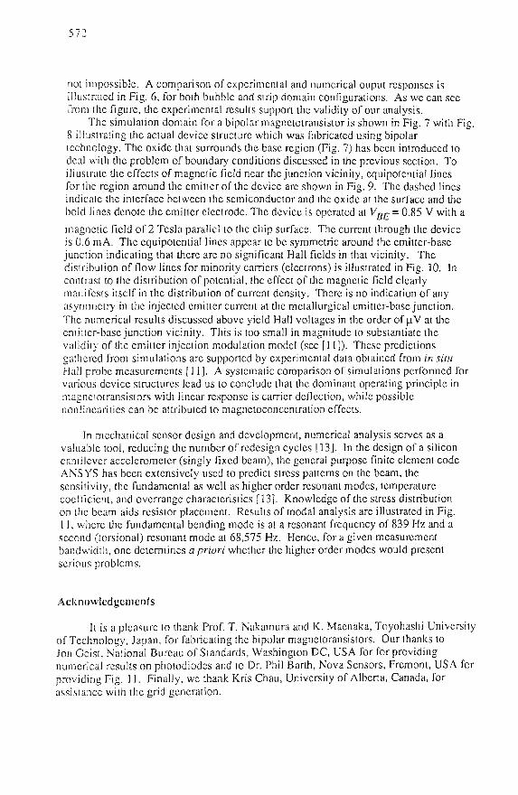
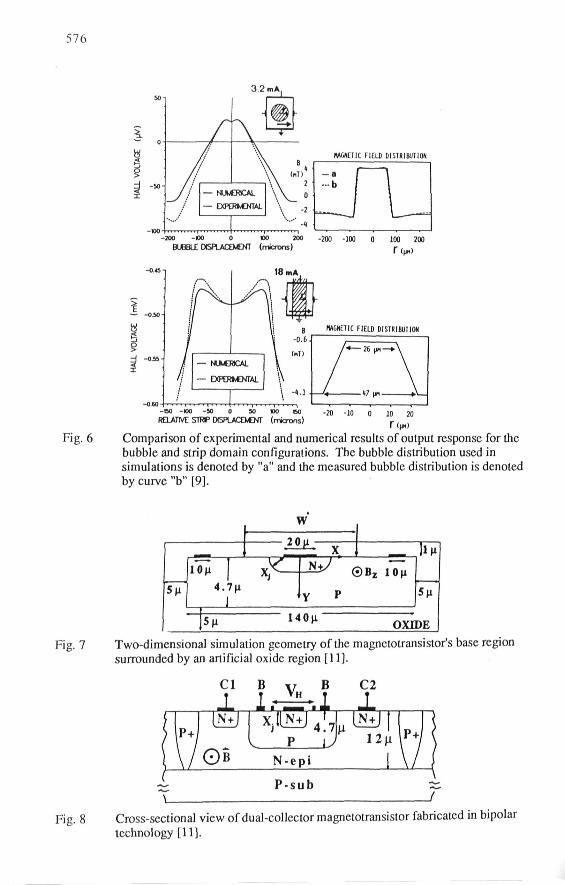
not impossible. A comparison of experimental and numerical ouput responses is illustrated in Fig. 6, for both bubble and strip domain configurations. As we can sec from (he figure, the experimental results support the validity of our analysis.
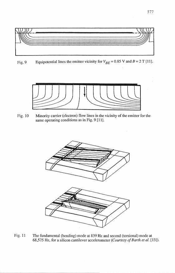
The simulation domain for a bipolar magnetotransistor is shown in Fig. 7 with Fig. 8 illustrating the actual device structure which was fabricated using bipolar technology. The oxide that surrounds the base region (Fig. 7) has been introduced to deal with the problem of boundary conditions discussed in the previous section. To illustrate the effects of magnetic field near the junction vicinity, cquipotcntial lines for the region around the emitter of the device arc shown in Fig. 9. The dashed lines indicate the interface between the semiconductor and the oxide at the surface and the bold lines denote the emitter electrode. The device is operated at Vnr = 0.85 V with a
magnetic field of 2 Tcsla parallel to the chip surface. The current through the device is 0.6 m A. The cquipotcntial lines appear to be symmetric around the emitter-base junction indicating that there arc no significant Hall fields in that vicinity. The distribution of flow lines for minority carriers (electrons) is illustrated in Fig. 10. In contrast to the distribution of potential, the effect of the magnetic field clearly manifests itself in the distribution of current density. There is no indication of any asymmetry in the injected emitter current at the metallurgical emitter-base junction. The numerical results discussed above yield Hall voltages in the order of (iV at the emitter-base junction vicinity. This is too small in magnitude to substantiate the validity of the emitter injection modulation model (see f 11]). These predictions gathered from simulations arc supported by experimental data obtained from in situ Hall probe measurements [11]. A systematic comparison of simulations performed for various device structures lead us to conclude that the dominant operating principle in magnctotransistors with linear response is carrier deflection, while possible nonlincaritics can be attributed to magnctoconccntration effects.
In mechanical sensor design and development, numerical analysis serves as a valuable tool, reducing the number of redesign cycles [13]. In the design of a silicon cantilever accclcrometcr (singly fixed beam), the general purpose finite clement code ANSYS has been extensively used to predict stress patterns on the beam, the sensitivity, the fundamental as well as higher order resonant modes, temperature coefficient, and ovcrrangc characteristics [13]. Knowledge of the stress distribution on the beam aids resistor placement. Results of modal analysis arc illustrated in Fig. 11, where the fundamental bending mode is at a resonant frequency of 839 Hz and a second (torsional) resonant mode at 68,575 Hz. Hence, for a given measurement bandwidth, one determines a priori whether the higher order modes would present serious problems.
Acknowledgement
It is a pleasure to thank Prof. T, Nakamura and K. Vlacnaka, Toyohashi University of Technology, Japan, for fabricating the bipolar magncloransistors. Our thanks to Jon Gcist, National Bureau of Standards, Washington DC, USA for for providing numerical results on phoiodiodcs and to Dr. Phil Barih, Nova Sensors, Fremont, USA for providing Fig. 11. Finally, we thank Kris Chau, University of Alberta, Canada, for assistance with the grid generation.
573
REFERENCES
[ 1 ] S. Middclhock and J. Van dcr Spiegel (Editors), State of the Art of Sensor Research and Development, reprint of Sensors and Actuators, 10, Elsevier Sequoia S. A„ Lausanne, 1986.
[2] H, P. Baltcs and R. S. Popovic, "Integrated semiconductor magnetic field sensors," Proc. IEEE, 74, pp. 1107-1132,1986.
[3] S. Kataoka (Chairman), Transducers '87, The 4lh International Conference on Solid-State Sensors and Actuators, Technical Digest, IEE Japan, Tokyo, 1987.
[41 S. D. Scnturia (Guest Editor), Special Issue on Microscnsors and Microactuators, IEEE Trans. Electron Devices, 35, pp. 711-808, 1988.
[5] R. S. Muller (Chairman), IEEE Solid State Sensor and Actuator Workshop, Technical Digest, IEEE Catalog Number 88TH0215-4, 1988.
16] J. L. Gray, Two-Dimensional Modeling of Silicon Solar Cells, Ph.D. dissertation, Purdue University, West Lafayette, USA, 1982.
[7] J. Gcist and H. P. Baltcs, "High accuracy modeling of photodiodc front-region quantum efficiency," Appl. Opt., submitted.
[8] A. Nathan, Carrier Transport in Magnetotransistors, Ph.D. dissertation, University of Alberta, Edmonton, Canada, 1988.
[9] A. Nathan, W. Allegretto, H, P. Baltes, and Y. Sugiyama, "Carrier transport in semiconductor magnetic domain detectors," IEEE Trans. Electron Devices, 34, pp. 2077-2085, 1987.
[10] W. Allegretto, A. Nathan, and H. P. Baltcs, "Two-dimensional numerical analysis of silicon bipolar magnetotransistors," Proc. NASECODE V Conference, J. J. H. Miller, Ed., Dublin: Boole Press, 1987, pp. 87-92.
[11] A, Nathan, K. Maenaka, W, Allegretto, H. P. Baltes, and T. Nakamura, "The Hall effect in magnetotransistors," IEEE Trans. Electron Devices, in press.
[12] K, W. Lee and K. D. Wise," "SENSIM": A simulation program for solid stale pressure sensors," IEEE Trans. Electron Devices, 29, pp. 34-41, 1982.
[13] P. W, Barlh, F. Pourahmadi, R. Mayer, J. Poydock, and K. Peterson, "A monolithic silicon accclerometcr with integral air damping and ovcrrangc protection," Technical Digest, IEEE Solid-Stale Sensor and Actuator Workshop, IEEE Catalog No, 88TH0215-4, pp. 35-38, 1988.
[14] S. Sclbcrhcrr, Analysis and Simulation of Semiconductor Devices, Vienna: Springcr-Vcrlag, 1984.
[ 15] G. C. M. Mcijcr, "Thermal sensors based on transistors," Sensors and Actuators, 10, pp. 103-125,1986.
[16] G. Baccarani, M. Rudan, R. Gucrricri, and P. Ciampolini, "Physical models for numerical device simulation," in Process and Device Modeling, W, L. Engl, Ed., Amsterdam: North Holland, pp. 107-158, 1986.
[17] A. W. van Hcrwaarden and P. M. Sarro, "Thermal sensors based on the Secbeck effect," Sensors and Actuators, 10, pp. 321-346, 1986.
[18] M.S. Lundstrom, R, J. Schwartz, and J. L. Gray, "Transport equations for the analysis of heavily doped semiconductor devices," Sol.-St. Electronics, 24, pp. 195-202, 1981.
[19] O. Madclung, Introduction to Solid State Theory, Berlin: Springer-Verlag, 1978. 120] V. Zicrcn, "Integrated silicon multicollcctor magnetotransistors," Ph.D.
dissertation, Delft University of Technology, Delft, The Netherlands, 1983. [21] A. C. Beer, Galvanomagnctic Effects in Semiconductors, New York: Academic
Press, 1963. [22] J. J. Woriman, J. R. Hauscr, and R. M, Burger, "Effect of mechanical stress on p-n
junction device characteristics," J. Appl. Phys., 35, pp. 2122-2131, 1964.
574
[23] B. Puers, L. Rcynaert, W. Snoeys, and W. M. C. Sansen, "A new uniaxial acccleromcter in silicon based on the piezojunction effect," IEEE Trans. Electron Devices, 35, pp. 764-770,1988.
[24] K. W. Lee, Modeling and Simulation of Solid State Pressure Sensors, Ph.D; dissertation, University of Michigan, Ann Arbor, USA, 1981.
[25] W. L. Engl, H. K. Dirks, and B. Meinerzhagen, "Device modeling," Proc. IEEE, 71, pp. 10-33,1983.
[26] B. Delauney, "Sur la sphere vide," Bull. Acad. Science USSR (VII), Classe Sci., Mat. Nat., pp. 793-800, 1934.
[27] B. Joe, "Delauney triangulation meshes in convex polygons," SI AM J. Sci. Stat. Comput., 7, pp. 514-539,1986.
[28] K. Y. K. Chau, Finite Element Mesh Generation/or Semiconductor Device Simulation, M.Sc. thesis, University of Alberta, Edmonton, Canada, 1988.
[29] G. Strang and G. F. Fix, An Analysis of the Finite Element Method, Englewood Cliffs, New Jersey: Prentice-Hall, 1973.
[30] I. Babuska and A. K. Aziz, "On the angle condition in the finite element method," SIAM Journal of Numerical Analysis, 13, pp. 214-216. 1976.
[31] R. E. Bank and D. J. Rose, "Parameter selection for Newton-like methods applicable to nonlinear partial differential equations," SIAM Journal of Numerical Analysis, 17, pp. 806-822,1980.
[32] W. Allegretto, A. Nathan, and H. P. Bakes," Numerical Analysis of magnctic-field-sensitive bipolar devices," IEEE Computer Aided Design, submitted.
[33] D. L. Scharfetter and H. K. Gummel, "Large-signal analysis of a silicon read diode oscillator," IEEE Trans. Electron Devices, 16, pp. 64-77, 1969.
[34] A. George and J. W. H. Liu, "The design of a user interface for a sparse matrix package," ACM Trans, on Math Software, 5, pp. 139-162, 1979.
diaphragm
Fig. 1. Cross-sectional view of a pressure transducer
Fig. 2 Triangular mesh for an emitter base junction of a magnctotransistor, generated using Delauney triangulation at junction sidewalls and regular grid triangulation everywhere else [8].

575
Fig. 3 Delaunay triangulation for a microbridgc with apertures {Courtesy ofChau [28]).
1 0 "
10'5
2 Q < 10'° K
O § 10s
O
r •• r - I
^ \ ^ H o l e s
-—--" Electrons
i I — i
"1
1 2 3 4
DEPTH (Mm)
Fig. 4 The electric field and carrier concentrations at equilibrium as a function of depth. The nominal front region parameters used are characteristic of the Hamamatsu 1337 photodiode {Courtesy ofGeist [7]).
03
o
03
t i
MSB,
-20 6 * » (pni)
,
°
tffc i
0 ((ml • 2 0 (pm)
Fig. 5 Equipotential and current lines for a Hall cross with longitudinal strip domain, a split-electrode Hall device with transverse strip domain, and a conventional Hall device with bubble domain [9].
576
3 . 2 mA
-200 -no o no 200 BUBBLE DISPLACEMENT (microns)
-200 -100 0 100 200
-BO -no - M O so no eo RELATIVE S T W DISPLACEMENT (microns)
-20 -10 0 10 20
Fig. 6 Comparison of experimental and numerical results of output response for the bubble and strip domain configurations. The bubble distribution used in simulations is denoted by "a" and the measured bubble distribution is denoted by curve "b" [9].
Fig. 7
Fig. 8
5u
10M
4.7M
1
5M
W
J=*l X
x^T X J
1
JteS c
Y P
DB,, 10M
1 4 ^ OXE
11H
5M
DE Two-dimensional simulation geometry of the magnetotransistor's base region surrounded by an artificial oxide region [11].
Cl B v
1 1:
P - s u b
Cross-sectional view of dual-collector magnctotransistor fabricated in bipolar technology [11].
577
Fig. 9 Equipotential lines the emitter vicinity for VBE = 0.85 V and B = 2 T [11].
Fig. 10 Minority carrier (electron) flow lines in the vicinity of the emitter for the same operating conditions as in Fig. 9 [11].
Fig. 11 The fundamental (bending) mode at 839 Hz and second (torsional) mode at 68,575 Hz, for a silicon cantilever accelerometer (Courtesy ofBarth et al. [13]).