simulink behavioral modeling of a 10-bit pipelined …...s. barra et al. / simulink behavioral...
TRANSCRIPT
International Journal of Automation and Computing 10(2), April 2013, 134-142
DOI: 10.1007/s11633-013-0706-0
Simulink Behavioral Modeling of a 10-bit Pipelined ADC
Samir Barra1 Souhil Kouda2 Abdelghani Dendouga3 N. E. Bouguechal11Advanced Electronics Laboratory, Department of Electronics, University of Batna, Avenue Chahid Boukhlouf Mohamed El Hadi, 05000,
Batna, Algeria2Department of electronics, University of M′sila, M′sila, Algeria
3Center for Development of Advanced Technologies, Microelectronics and Nanotechnology Division, August 20 1956 City, BP 17, BabaHassen, Algiers, Algeria
Abstract: The increasing architecture complexity of data converters makes it necessary to use behavioral models to simulate theirelectrical performance and to determine their relevant data features. For this purpose, a specific data converter simulation environmenthas been developed which allows designers to perform time-domain behavioral simulations of pipelined analog to digital converters(ADCs). All the necessary blocks of this specific simulation environment have been implemented using the popular Matlab simulinkenvironment. The purpose of this paper is to present the behavioral models of these blocks taking into account most of the pipelinedADC non-idealities, such as sampling jitter, noise, and operational amplifier parameters (white noise, finite DC gain, finite bandwidth,slew rate, and saturation voltages). Simulations, using a 10-bit pipelined ADC as a design example, show that in addition to the limitsanalysis and the electrical features extraction, designers can determine the specifications of the basic blocks in order to meet the givendata converter requirements.
Keywords: Behavioral modeling, analog to digital converters (ADCs), pipelined ADC, multiple digital to analog converter (MDAC),sample and hold (S/H).
1 IntroductionData converters, analog to digital converter (ADC) and
digital to analog converter (DAC), play a fundamental rolein interfacing the digital processing core with the outerreal analog world. ADCs can be found in a wide rangeof applications, spanning from imaging to ultrasound andcommunication systems. In particular, pipelined ADCarchitecture[1, 2] offers a good trade-off between conversionrate, resolution and power consumption.
Traditionally, modeling of analog and mixed signalblocks, such as data converters, has been realized at devicelevel or at a lower functional level. This gives good accuracyand allows good modeling of the non-ideal effects presentin the data converter (noise, distortion, mismatching, etc.),but the simulation time increases drastically and technol-ogy and architecture independence can be lost. However,with the increasing complexity of designs, the need for ac-curate and speedy models has produced a change to thecurrent trend towards behavior modeling. Out of differentapproaches, the so-called “behavioral modeling” reproducesthe required behavior of the original analyzed system.
This approach is motivated by the aim of obtaining amodel for analysis and synthesis that respects the underly-ing physics and sets up the appropriate mathematical con-cepts from there.
Behavioral modeling uses the mathematical characteris-tics of each block to describe the behavior of the wholepipelined ADC. It achieves one of the best trade-offs be-tween speed and accuracy because pre-calculated, parame-terized closed-form expressions, instead of state equations,are employed to capture the dynamic behavior of analogblocks. The larger the number of non-idealities embeddedinto these closed-forms expressions and the more the analy-sis of the impact of these non-idealities involved, the betterthe behavioral models[3].
Manuscript received June 19, 2012; revised October 11, 2012
Research groups working in the area of behavioral mod-eling for pipelined ADCs use different high level languagesand alternate approaches like Matlab simulink[3−6], VHDL-AMS[7, 8] and Spice[9]. Event-driven behavioral models havebeen previously employed to support the design of pipelinedADCs[3−6]. However, these previous models have somedrawbacks as they mostly take into account only a fewsources of error. In this paper, the purpose of modelingis analyzing the non-idealities in the pipelined ADC for op-timizing accuracy and linearity parameters of the converterto predict static and dynamic performance.
This paper focuses on the behavioral modeling ofpipelined ADCs implemented in the very popular Matlabsimulink environment. The new toolbox includes a com-plete set of pipelined ADC circuit models that take into ac-count the main non-idealities which degrade the converterperformance considerably. These models are implementedby combining elementary simulink library blocks in orderto keep the computational cost minimum. The most sig-nificant non-idealities are modeled and building blocks formodeling sampling jitter, noise, and operational amplifierparameters (white noise, finite DC gain, finite bandwidth,slew rate (SR) and saturation voltages) are proposed.
This paper is organized as follows. In Section 2, the corre-sponding behavioral model blocks are presented. The majornon-idealities of pipelined ADCs are described in Section3. Finally, in Section 4, we report the simulation resultsobtained using the proposed blocks for a 10-bit pipelinedADC.
2 Behavioral modeling of pipelinedADCs
The pipelined ADC is constructed using switched capac-itor (SC) circuits, which exploit the charge storing abilitiesof complementary metal oxide semiconductor (CMOS) to
S. Barra et al. / Simulink Behavioral Modeling of a 10-bit Pipelined ADC 135
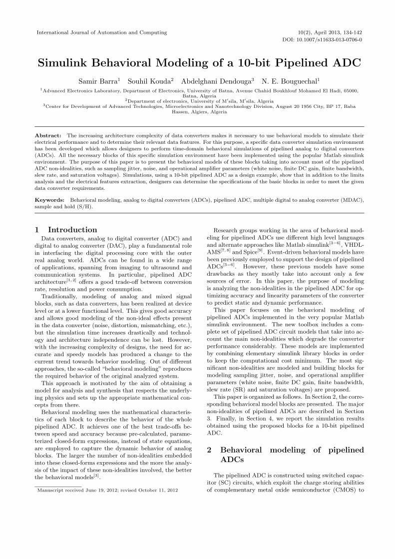
achieve precise signal processing and which is preferred inmixed signal and analog-to-digital converter (A/D) inter-faces. The conceptual block diagram of a generic pipelinedADC, consisting of an arbitrary cascade of k stages and asample-and-hold (S/H) circuit at the front[3] is shown inFig. 1 (a). Each stage resolves partial code words of lengthni, i = 1, · · · , k, which are all re-ordered and combined atthe digital correction block to obtain the output of the con-verter. The inner structure of a pipeline stage comprisesof four blocks, as illustrated in Fig. 1 (b) a flash sub-ADCwith Ni 6 2n
i output codes, a sub-DAC with Ni output lev-els, a substractor, and an S/H residue amplifier with gainGi. The latter three blocks are implemented in practice bya single subcircuit which is often referred to as multiply-ing digital to analog converter (MDAC). We combine theblocks of the sub-ADC and the MDAC together to get asingle pipelined stage.
Fig. 1 Block diagram of a pipelined ADC
2.1 Sample-and-hold circuit
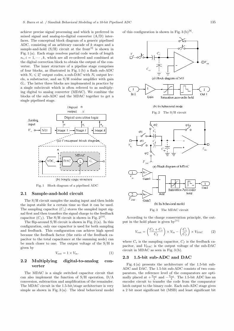
The S/H circuit samples the analog input and then holdsthe input stable for a certain time so that it can be used.The sampling capacitor (Cs) stores the sampled input sig-nal first and then transfers the signal charge to the feedbackcapacitor (Cf ). The S/H circuit is shown in Fig. 2[10].
The flip-around S/H circuit is shown in Fig. 2 (a). In thisconfiguration, only one capacitor is used for both samplingand feedback. This configuration can achieve high speedbecause the feedback factor (the ratio of the feedback ca-pacitor to the total capacitance at the summing node) canbe much closer to one. The output voltage of the S/H isgiven by
Vout = 1× Vin. (1)
2.2 Multiplying digital-to-analog con-verter
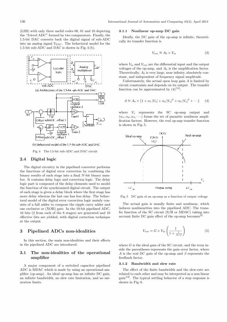
The MDAC is a single switched capacitor circuit thatcan also implement the function of S/H operation, D/Aconversion, subtraction and amplification of the remainder.The MDAC circuit in the 1.5-bit/stage architecture is verysimple as shown in Fig. 3 (a). The ideal behavioral model
of this configuration is shown in Fig. 3 (b)[9].
Fig. 2 The S/H circuit
Fig. 3 The MDAC circuit
According to the charge conservation principle, the out-put in the hold phase is given by[11]
Vout =
(Cf + Cs
Cf
)× Vin −
(Cs
Cf
)× VDAC (2)
where Cs is the sampling capacitor, Cf is the feedback ca-pacitor, and VDAC is the output voltage of the sub-DACcircuit in MDAC as seen in Fig. 3 (b).
2.3 1.5-bit sub-ADC and DAC
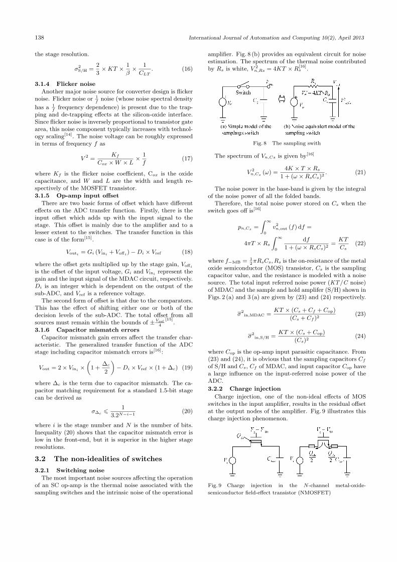
Fig. 4 (a) presents the architecture of the 1.5-bit sub-ADC and DAC. The 1.5-bit sub-ADC consists of two com-parators, the reference level of the comparators are opti-mally placed at +Vref
4and −Vref
4. The 1.5-bit ADC has an
encoder circuit to transfer the code from the comparatorlatch output to the binary code. Each sub-ADC stage givesa 2 bit most significant bit (MSB) and least significant bit
136 International Journal of Automation and Computing 10(2), April 2013
(LSB) with only three useful codes 00, 01 and 10 depictingthe “3-level ADC” formed by two comparators. Finally, the1.5-bit DAC converts back the digital signal of sub-ADCinto an analog signal VDAC. The behavioral model for the1.5-bit sub-ADC and DAC is shown in Fig. 4 (b).
Fig. 4 The l.5-bit sub-ADC and DAC circuit
2.4 Digital logic
The digital circuitry in the pipelined converter performsthe functions of digital error correction by combining thebinary results of each stage into a final N -bit binary num-ber. It contains delay logic and correction logic. The delaylogic part is composed of the delay elements used to modelthe function of the synchronized digital circuit. The outputof each stage is given a delay block where the first stage hasmore delay whereas the last one has less delay. The behav-ioral model of the digital error correction logic mainly con-sists of a full adder to compose the ripple carry adder andone exclusive or (XOR) gate. In the 10-bit pipelined ADC,16 bits (2 from each of the 8 stages) are generated and 10effective bits are yielded, with digital correction techniqueat the output.
3 Pipelined ADCs non-idealities
In this section, the main non-idealities and their effectsin the pipelined ADC are introduced.
3.1 The non-idealities of the operationalamplifier
A major component of a switched capacitor pipelinedADC is MDAC which is made by using an operational am-plifier (op-amp). An ideal op-amp has an infinite DC gain,an infinite bandwidth, no slew rate limitation, and no sat-uration limits.
3.1.1 Nonlinear op-amp DC gain
Ideally, the DC gain of the op-amp is infinite, theoreti-cally its transfer function is
Vout∼= A0 × Vin (3)
where Vin and Vout are the differential input and the outputvoltages of the op-amp, and A0 is the amplification factor.Theoretically, A0 is very large, near infinity, absolutely con-stant, and independent of frequency signal amplitude.
Unfortunately, the actual open loop gain A is limited bycircuit constraints and depends on its output. The transferfunction can be approximated by (4)[12]:
A ∼= A0 ×(1 + α1 |Vo|+ α2 |Vo|2 + α3 |Vo|3 + · · ·) (4)
where Vo represents the SC op-amp output and(α1, α2, α3, · · · ) forms the set of parasitic nonlinear ampli-fication factors. However, the real op-anp transfer functionis shown in Fig. 5.
Fig. 5 DC gain of an op-amp as a function of output voltage
The actual gain is usually finite and nonlinear, whichinduces nonlinearities into the pipelined ADC. The trans-fer function of the SC circuit (S/H or MDAC) taking intoaccount finite DC gain effect of the op-amp becomes[8]
Vout = G× Vin
(1
1 + 1A×β
)(5)
where G is the ideal gain of the SC circuit, and the term in-side the parentheses represents the gain error factor, whereA is the real DC gain of the op-amp and β represents thefeedback factor.
3.1.2 Bandwidth and slew rate
The effect of the finite bandwidth and the slew-rate arerelated to each other and may be interpreted as a non-lineargain[12]. The typical settling behavior of a step response isshown in Fig. 6.

S. Barra et al. / Simulink Behavioral Modeling of a 10-bit Pipelined ADC 137
Fig. 6 Typical settling behavior of the step response
In the initial settling period, the slope of the output sig-nal is limited by the SR of the op-amp. Once the slope ofoutput signal is less than SR, the response goes into thelinear mode. The transition point in time between them isat t0. We add the settling error behavior into (3). Thisresponse is given by
Vout = G× Vin
(1
1 + 1A×β
) (1− e−
tτ
). (6)
The exponential term in the second bracket represents thesettling error of the single pole op-amp, and τ = 1
2πβGBW
is the time constant of the SC circuit, where GBW andβ are the unity gain frequency and feedback factor of theSC circuit respectively. The slope of this curve reaches itsmaximum value when t = 0, resulting in
d
dtvout(t)
∣∣∣∣maxt=0
=
G× Vin
(1
1+ 1A×β
)
τ. (7)
We must consider two separate cases[13]:1) The value specified by (7) is lower than the operational
amplifier SR. In this case, there is no SR limitation and theevolution of Vout conforms to (6).
2) The value specified by (7) is larger than SR. The op-amp is in slewing mode. Therefore, the first part of thetransient response of Vout is limited by SR, and in the otherpart, it reverts to the linear settling mode behavior after t0.
t < t0 : Vout = SR× t (8)
t > t0 : Vout = Vout (t0)+(VinG− SR× t0)×(1− e−
t−t0τ
).
(9)Imposing the condition for the continuity of the derivativesof (8) and (9) in t0, we obtain
t0 =Vin ×G
SR− τ. (10)
If t0 > Ts2
, (8) holds for the whole hold clock period. Theallowed total settling time is
Tsettling =1
2× fs(11)
where fs(fs = 1Ts
) is the sampling frequency, and Ts is thesampling period.
3.1.3 Op-amp thermal noise
The intrinsic thermal noise of the op-amp is the mostimportant noise source affecting the operation of both theswitched capacity (SC) MDAC and the S/H. The calcula-tion of op-amp thermal noise is dependent on the op-amparchitecture. We first assume that the noise sources in-clude only the noises produced by input transistors in thedifferential pair. Fig. 7 presents a simple one pole model tocalculate op-amp noise.
Fig. 7 AC model for op-amp noise calculation
The transfer function of this model is
H(s) =V0
in=
r0
(1 + gm× r0 × β)×(1 + s×CLT×r0
1+gm×r0×β
)
(12)where β is the feedback factor, in is the noise current sourcewhich can be seen at the right side of Fig. 7, CLT is the to-tal load capacitance given by CLT = CL + β(Cs + Cop),CL is the load capacitor, Cop is the input capacitor of theop-amp, and gm is the transconductance of the metal ox-ide semiconductor field effect transistor (MOSFET) metaloxide semiconductor field effect transistor.
The noise current source can be written as
i2n = γ × 4KT × gm×∆f (13)
where γ is a coefficient equal to 23
for long channel tran-sistors, K is the Boltzmann constant, T is the absolutetemperature, and ∆f is a small bandwidth at frequency f .So the input-referred noise power can be expressed as
V2in =
V20
G2=
∫∞0
(∣∣∣H(
s|jω
)∣∣∣2
× i2n
)
G2=
2
3×KT × 1
β× 1
CLT×
(Cf
Cs + Cf
)(14)
where G is the gain of the MDAC. The op-amps in S/H andMDAC are the same. The only difference is that there isonly one capacitor for sampling and holding in S/H. How-ever, there are two capacitors Cs and Cf in MDAC adshown in Fig. 3 (a). So it is easy to get the input-referrednoise of S/H if Cs and β in (14) are set to be 0 and 1.
σ2MDAC =
2
3×KT × 1
β× 1
CLT×
(Cf
Cs + Cf
)(15)
where β = Cs
2B×Cs+Cop, CLT = CL + β(Cs + Cop), and B is
138 International Journal of Automation and Computing 10(2), April 2013
the stage resolution.
σ2S/H =
2
3×KT × 1
β× 1
CLT. (16)
3.1.4 Flicker noise
Another major noise source for converter design is flickernoise. Flicker noise or 1
fnoise (whose noise spectral density
has a 1f
frequency dependence) is present due to the trap-ping and de-trapping effects at the silicon-oxide interface.Since flicker noise is inversely proportional to transistor gatearea, this noise component typically increases with technol-ogy scaling[14]. The noise voltage can be roughly expressedin terms of frequency f as
V 2 =Kf
Cox ×W × L× 1
f(17)
where Kf is the flicker noise coefficient, Cox is the oxidecapacitance, and W and L are the width and length re-spectively of the MOSFET transistor.3.1.5 Op-amp input offset
There are two basic forms of offset which have differenteffects on the ADC transfer function. Firstly, there is theinput offset which adds up with the input signal to thestage. This offset is mainly due to the amplifier and to alesser extent to the switches. The transfer function in thiscase is of the form[15].
Vouti = Gi (Vini + Voffi)−Di × Vref (18)
where the offset gets multiplied up by the stage gain, Voffi
is the offset of the input voltage, Gi and Vini represent thegain and the input signal of the MDAC circuit, respectively.Di is an integer which is dependent on the output of thesub-ADC, and Vref is a reference voltage.
The second form of offset is that due to the comparators.This has the effect of shifting either one or both of thedecision levels of the sub-ADC. The total offset from allsources must remain within the bounds of ±Vref
4
[15].
3.1.6 Capacitor mismatch errors
Capacitor mismatch gain errors affect the transfer char-acteristic. The generalized transfer function of the ADCstage including capacitor mismatch errors is[16]:
Vout = 2× Vini ×(
1 +∆c
2
)−Di × Vref × (1 + ∆c) (19)
where ∆c is the term due to capacitor mismatch. The ca-pacitor matching requirement for a standard 1.5-bit stagecan be derived as
σ∆c 6 1
3.2N−i−1(20)
where i is the stage number and N is the number of bits.Inequality (20) shows that the capacitor mismatch error islow in the front-end, but it is superior in the higher stageresolutions.
3.2 The non-idealities of switches
3.2.1 Switching noise
The most important noise sources affecting the operationof an SC op-amp is the thermal noise associated with thesampling switches and the intrinsic noise of the operational
amplifier. Fig. 8 (b) provides an equivalent circuit for noiseestimation. The spectrum of the thermal noise contributedby Rs is white, V 2
n,Rs = 4KT ×R[16]s .
Fig. 8 The sampling swith
The spectrum of Vn,Cs is given by[16]
V 2n,Cs
(ω) =4K × T ×Rs
1 + (ω ×RsCs)2. (21)
The noise power in the base-band is given by the integralof the noise power of all the folded bands.
Therefore, the total noise power stored on Cs when theswitch goes off is[16]
pn,Cs =
∫ ∞
0
v2n,out (f) df =
4πT ×Rs
∫ ∞
0
df
1 + (ω ×RsCs)2=
KT
Cs(22)
where f−3dB = 12πRsCs, Rs is the on-resistance of the metal
oxide semiconductor (MOS) transistor, Cs is the samplingcapacitor value, and the resistance is modeled with a noisesource. The total input referred noise power (KT/C noise)of MDAC and the sample and hold amplifer (S/H) shown inFigs. 2 (a) and 3 (a) are given by (23) and (24) respectively.
σ2in,MDAC =
KT × (Cs + Cf + Cop)
(Cs + Cf )2(23)
σ2in,S/H =
KT × (Cs + Cop)
(Cs)2(24)
where Cop is the op-amp input parasitic capacitance. From(23) and (24), it is obvious that the sampling capacitors Cf
of S/H and Cs, Cf of MDAC, and input capacitor Cop havea large influence on the input-referred noise power of theADC.
3.2.2 Charge injection
Charge injection, one of the non-ideal effects of MOSswitches in the input amplifier, results in the residual offsetat the output nodes of the amplifier. Fig. 9 illustrates thischarge injection phenomenon.
Fig. 9 Charge injection in the N -channel metal-oxide-
semiconductor field-effect transistor (NMOSFET)

S. Barra et al. / Simulink Behavioral Modeling of a 10-bit Pipelined ADC 139
When the MOS switch is on and its drain-source voltageVds is small, the charge under the gate oxide resulting fromthe inverted channel is approximated by[17]
Qch = COX ×W × L× (VGS − VTH). (25)
Thus, when the MOS transistor is switched off, half ofthe channel charge is sent to Cload. As the accumulatedcharges in n-channel and p-channel transistors are electronsand holes, respectively, the charge injection of n-channeland p-channel switches will result in negative and positivespikes correspondingly. Their amplitude, for instance, in anN -channel metal-oxide-semiconductor field-effect transistor(NMOS) switch can be calculated by
∆Vinj = −Qch
C= −COX ×W × L× (VGS − VTH)
2× Cload. (26)
Assuming that the clock swings between VDD and VSS, weobtain
∆Vinj = −COX ×W × L× (VDD − Vin − VTH)
2× Cload(27)
where Vin represents the input signal.3.2.3 Clock feedthrough
In addition to channel charge injection, an MOS switchcouples the clock transitions to the sampling capacitorthrough its gate-drain and gate-source overlap capacitance.Depicted in Fig. 10, the effect introduces an error at theoutput. Assuming the overlap capacitance Cov is constant,the error can be expressed as[18]:
∆Vclk = VclkCov
Cov + CH(28)
where Vclk is the clock signal voltage, Cov is the overlapcapacitor per unit width, and CH is the hold capacitor.This voltage error is independent of the input level.
Fig. 10 Clock feedthrough in a sampling circuit
3.2.4 Nonlinear on-resistance
In actual implementations of SC circuits, on-resistanceof the MOS switch can have a significant effect on the set-tling time of the circuit. Nonlinear on-resistance which is asignal-dependent variation of the on-resistance of the switchintroduces harmonic distortion into the circuit. In addition,the one pole system composed of the finite turn-on resis-tance of switch (R) and sampling capacitor (C) shown inFig. 11 determines the bandwidth of the input signal in SCcircuits. The sampled input voltage is given by
Vin,s = Vin ×(1− e−
tτ
)(29)
where τ = R× C.Fig. 11 presents a simple MOS S/H circuit and its equiva-
lent model for calculation of on-resistance noise in the MOSswitch.
Fig. 11 A simple S/H circuit and its equivalent model for noise
calculation
The nonlinear turn-on resistance can be extracted fromthe plot of switch resistance, and by using curve fitting. Wehave obtained a polynomial function, which can be used tomodel the effect caused by the nonlinear “on” resistance ofthe switch. Fig. 12 shows the behavioral model of the finiteturn-on resistance of the switch.
Fig. 12 Modeling the effect of the nonlinear finite turn-on resis-
tance
3.3 Clock jitter
Jitter is defined as a random variation of sampling in-stants. Clock generator phase noise and sampling circuitare the cause of jitter[18]. Noise introduced by jitter canbe assumed to be white, i.e, it is uniformly distributed be-tween frequencies 0 to fs
2. Jitter error can be reduced by
oversampling the input signal. The clock jitter value of asampled signal is represented as[19]
x′i (t) = xi (t) + δ × [xi (t + 1)− xi (t)]× fs (30)
where x′i (t) is the error due to the jitter deviation of δ insample value xi(t) with a true sampling frequency fs. UsingTaylor′s series expansion, we have[19]
δ × [xi (t + 1)− xi (t)] fs ≈ δ × d
dtxi (t) . (31)
Clock jitter results in a non-uniform sampling time se-quence, and produces an error which increases the totalerror power at the spectrum output of the whole pipelinedADC. This phenomenon can be observed from Fig. 13. Thiserror is introduced when a sinusoidal signal x(t) with am-plitude A and frequency fin is sampled at an instant which
140 International Journal of Automation and Computing 10(2), April 2013
is in error by an amount δ and is given by[20].
x (t + δ)− x (t) ≈2π × fin × δ ×A× cos (2πfint) =
δ × dx(t)
dt. (32)
Fig. 13 Clock jitter error
Here, we assumed that the sampling uncertainty δ is aGaussian random process with a standard deviation ∆τ [19].Fig. 14 shows the behavioral model of the effect describedby (32).
Fig. 14 Clock jitter model
4 Simulation results
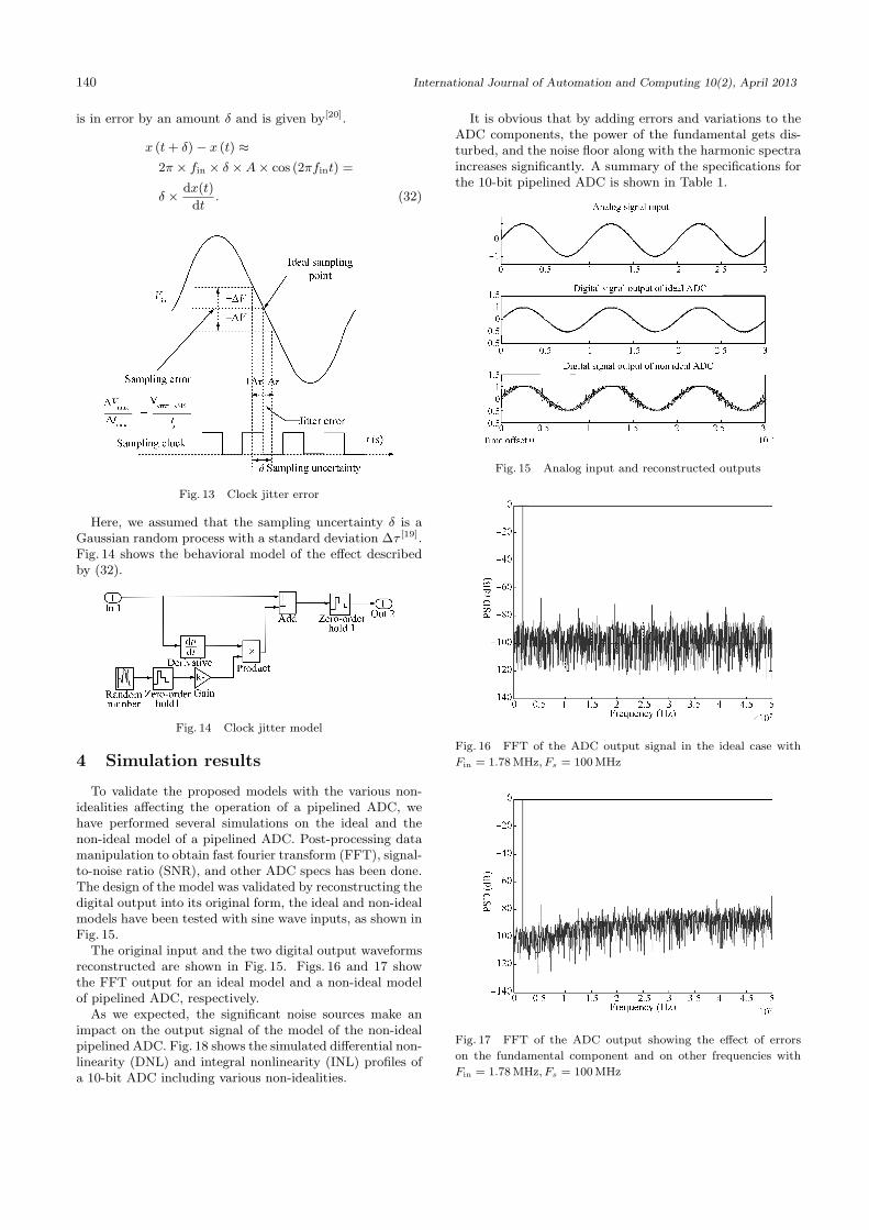
To validate the proposed models with the various non-idealities affecting the operation of a pipelined ADC, wehave performed several simulations on the ideal and thenon-ideal model of a pipelined ADC. Post-processing datamanipulation to obtain fast fourier transform (FFT), signal-to-noise ratio (SNR), and other ADC specs has been done.The design of the model was validated by reconstructing thedigital output into its original form, the ideal and non-idealmodels have been tested with sine wave inputs, as shown inFig. 15.
The original input and the two digital output waveformsreconstructed are shown in Fig. 15. Figs. 16 and 17 showthe FFT output for an ideal model and a non-ideal modelof pipelined ADC, respectively.
As we expected, the significant noise sources make animpact on the output signal of the model of the non-idealpipelined ADC. Fig. 18 shows the simulated differential non-linearity (DNL) and integral nonlinearity (INL) profiles ofa 10-bit ADC including various non-idealities.
It is obvious that by adding errors and variations to theADC components, the power of the fundamental gets dis-turbed, and the noise floor along with the harmonic spectraincreases significantly. A summary of the specifications forthe 10-bit pipelined ADC is shown in Table 1.
Fig. 15 Analog input and reconstructed outputs
Fig. 16 FFT of the ADC output signal in the ideal case with
Fin = 1.78MHz, Fs = 100MHz
Fig. 17 FFT of the ADC output showing the effect of errors
on the fundamental component and on other frequencies with
Fin = 1.78MHz, Fs = 100MHz

S. Barra et al. / Simulink Behavioral Modeling of a 10-bit Pipelined ADC 141
Fig. 18 DNL and INL of the non ideal 10-bit pipelined ADC
Table 2 shows the simulated DNL and INL profiles andother performance such as SNR, signal-to-noise and distor-tion ratio (SNDR) and spurious-free dynamic ratio (SFDR)The DNL is found to be −1/+1LSB, and the INL is−0.6/+1LSB. The SFDR is around −59 dB. We can noticethat the SNR degrades when the sources of noise includ-ing clock jitter, the thermal noise of the switches (KT/C )and the op-amp non-idealities (finite gain, finite bandwidth,slew-rate and saturations) are added into the non-idealmodel of the ADC. The agreement between the ideal modelof ADC and the non-ideal model of ADC simulations is no-ticeable. The comparison of our behavioral model perfor-mance (SNR, SNDR, INL, etc.) to other updated behaviormodels is not straightforward because very few simulationresults can be found in the literature of recent years[4, 5].A comparison between our behavioral model, including themain non-ideal effects, and real ADCs[1, 2] can be seen inTable 2. There is a good match between the proposedmodel and the real ADCs with little difference for SNDRand SFDR. This proves the accuracy of our behavior mod-els. Table 2 summarizes the simulated ADC performance.
Table 1 Specifications of the 10-bit pipelined ADC
Parameter Value
Technology TSMC 0.18 µm
Length of MOS transistor L 0.180 µm
Width of the MOS transistor W 0.270 µm
Resolution 10 bits
Sample capacitor and feedback capacitor Cs = Cf = 0.4 pF
Input capacitor of the op-amp Cop 0.13 pF
Hold capacitance CH 1 pF
Overlap capacitance COV 0.08 fF
Oxide capacitance COX 8.78F/m2
Sampling frequency fs 100MHz
Allowed total settling Tsetling 5 ns
Feedback factor of MDAC β 0.5
Feedback factor of S/H β 1.42
Time constant τMDAC 0.30 ns
Time constant τS/H 0.17 ns
Flicker noise coefficient Kf 3.10−12V 2.pF
Table 2 ADC performance
ParametersThis work/ This work/non-
[1] [2]ideal model ideal model
INL (LSB) −0.3/+0.3 −0.6/+1 −0.6/+0.8 −0.73/+0.73
DNL (LSB) −0.3/+0.2 −1/+1 −1/+0.7 −1.44/+1.44
SNR (dB) 66.86 63.66 * *
SFDR (dB) 62.95 59.66 65 64.8
SNDR (dB) 66.87 63.68 54 53.6
Resolution (bit) 10 10 10 10
Technology (µm) 0.18 0.18 0.18 0.18
5 Conclusions
A design and simulation environment for medium res-olution high speed pipelined ADC architectures was pro-posed. Both its ideal and non-ideal models were imple-mented and verified successfully in Matlab simulink usinga 10-bit pipelined ADC with a 1.5-bit per stage architec-ture. The proposed set of models takes into account at thebehavioral level most of the pipelined ADC non idealities,such as sampling jitter, noise, and operational amplifier pa-rameters (white noise, finite direct current gain, finite bandwidth and slew rate). We have shown that with a properdesign environment, we simply define the proper input stim-ulus and we can perform specific processing of the outputdata. A library of behavioral models of basic blocks per-mits to quickly implement the behavioral description of anydata converter architecture. If the behavioral model of thebasic blocks is customized using key electrical parameters,the behavioral simulation will permit the designer to ana-lyze the contribution of these parameters to the limits andto define specific blocks.
References
[1] S. W. Sin, U. Seng-Pan, R. P. Martins. 1. 2-V, 10-bit, 60–360 MS/s time-interleaved pipelined analog-to-digital con-verter in 0.18µm CMOS with minimised supply headroom.IET Circuits Devices & Systems, vol. 4, no. 1, pp. 1–3, 2010.
[2] J. F. Lin, S. J. Chang, C. C. Liu, C. H. Huang. A 10-bit 60-MS/s low-power pipelined ADC with split-capacitorCDS technique. IEEE Transactions on Circuits and Sys-tems, vol. 57, no. 3, pp. 163–167, 2010.
[3] E. Bilhan, P. C. Estrada-Gutierrez, A. Y. Valero-Lopez,F. Maloberti. Behavioral model of pipeline ADC by usingSIMULINK (R). In Proceedings of Southwest Symposiumon Mixed-signal Design, IEEE, Austin, TX, USA, pp. 147–151, 2001.
[4] M. Ramalatha, A. P. Karthick, S. Karthick, K. Muralikr-ishnan. A high speed 12-bit pipelined ADC using switchedcapacitor and fat tree encoder. In Proceedings of Interna-tional Conference on Advances in Computational Tools forEngineering Applications, IEEE, Zouk Mosbeh, Lebanon,pp. 391–395, 2009.
[5] J. Ruiz-Amaya, M. Delgado-Restituto, A. Rodrıguez-Vazquez. Behavioral modeling of pipeline ADC buildingblocks. International Journal of Circuit Theory and Appli-cations, vol. 40, no. 6, pp. 571–594, 2012.
[6] E. Mancini, S. Rapuano, D. Dallet. A distributed testsystem for pipelined ADCs. Measurement, vol. 42, no. 1,pp. 38–43, 2009.

142 International Journal of Automation and Computing 10(2), April 2013
[7] A. J. Acosta, E. J. Peralıas, A. Rueda, J. L. Huertas. HDLbehavioral modelling of pipeline analog to digital convert-ers. Measurement, vol. 31, no. 1, pp. 47–60, 2002.
[8] J. A. Diaz-Madrid, G. Domenech-Asensi, J. A. Lpez-Alcantud, H. Neubauer. VHDL-AMS model of A 40MS/s 12bit pipeline ADC. In Proceedings of International Confer-ence on Mixed Design of Integrated Circuits and Systems,IEEE, Gdynia, Poland, pp. 555–560, 2006.
[9] G. Zareba, O. A. Palusinski. Behavioral simulator of analog-to-digital converters for telecommunication applications. InProceedings of IEEE International Conference on Behav-ioral Modeling and Simulation, San Jose, California, USA,pp. 135–140, 2004.
[10] J. F. Lin, S. J. Chang, T. C. Kung, H. W. Ting, C.H. Huang. Transition-code based linearity test method forpipelined ADCs with digital error correction. IEEE Trans-actions on Very Large Scale Integration Systems, vol. 19,no. 12, pp. 2158–2169, 2011.
[11] J. F. Lin, S. J. Chang. A high speed pipelined analog-to-digital converter using modified time-shifted correlated dou-ble sampling technique. In Proceedings of IEEE Interna-tional Symposium on Circuits and Systems, IEEE, Islandof Kos, Greece, pp. 5367–5370, 2006.
[12] B. D. Sahoo, B. Razavi. U-PAS: A user-friendly ADC sim-ulator for courses on analog design. In Proceedings of IEEEInternational Conference on Microelectronics Systems Ed-ucation, IEEE, San Francisco, CA, USA, pp. 77–80, 2009.
[13] P. Malcovati, S. Brigati, F. Francesconi, F. Maloberti, P.Cusinato, A. Baschirotto. Behavioral modeling of switched-capacitor sigma–delta modulators. IEEE Transactions onCircuits and Systems I: Fundamental Theory and Applica-tions, vol. 50, no. 3, pp. 352–364, 2003.
[14] Y. Tsividis. Operation and Modeling of the MOS Transis-tor, 2nd ed., Boston: McGraw-Hill, 1999.
[15] P. J. Quinn, A. H. M. van Roermund. Accuracy limitationsof pipelined ADCs. In Proceedings of IEEE InternationalSymposium on Circuits and Systems ISCAS, IEEE, Kobe,Japan, vol. 3, pp. 1956–1959, 2005.
[16] F. Maloberti. Data Converters, Netherland: Springer Ver-lag, pp. 22–23, 2007.
[17] L. Dai, R. Harjani. CMOS switched-op-amp-based sample-and-hold circuit. IEEE Journal of Solid-State Circuits,vol. 35, no. 1, pp. 109–113, 2000.
[18] C. Eichenberger, W. Guggenbuhl. On charge injection inanalog MOS switches and dummy switch compensationtechniques. IEEE Transactions on Circuits and Systems,vol. 37, no. 2, pp. 256–264, 1990.
[19] S. Barra, A. Dendouga, S. Kouda, N. E. Bouguechal. Con-tribution to the analysis and modeling of the non-ideal ef-fects of pipelined ADCs using MATLAB. Journal of CircuitsSystems and Computers, vol. 22, no. 2, 1250085, 2013.
[20] A. Dendouga, N. E. Bouguechal, S. Kouda, S. Barra, B.Lakehal. Contribution to the modeling of a non-ideal Sigma-delta modulator. Journal of Computational Electronics,vol. 11, no. 4, pp. 321–329, 2012.
Samir Barra received the B.Eng. degreefrom University of Batna, Algeria, and theM. Sc. degree from University of Batna in2002 and 2008, respectively. From 2003 to2005, he was with the Satel Telecommuni-cation Company in Batna. Currently, heis a teacher in the Department of Scienceand Technology at the University of Batna,Algeria.
His research interests include microelec-tronics, sensors, digital, analog circuit design and mixed circuits,ADC design automation, and genetic algorithm.
E-mail: [email protected] (Corresponding author)
Souhil Kouda received the B.Eng. de-gree from University of Batna, Algeria, andthe M. Sc. degree from University of Batnain 2003 and 2008, respectively. Currently,he is a teacher in the Department of Elec-tronics at the University of Msila, Algeria.
His research interests include sensors,neural networks, modeling, and analog cir-cuit and mixed circuit design.
E-mail: [email protected]
Abdelghani Dandougua received theB.Eng. degree from University of Batna,Algeria, and the M. Sc. degree from Univer-sity of Batna in 2003 and 2008, respectively.Currently, he is a researcher in the Centerfor Development of Advanced Technologies,Microelectronics and Nanotechnology Divi-sion.His research interests include sensors, dig-ital, and analog circuit design and mixed
circuit, ADC design, and sigma delta ADC.E-mail: dendouga [email protected]
N. E. Bouguechal received the degreeof the electronics engineer from NationalPolytechnical School of Algiers in 1976, andreceived the M. Sc. degree in nuclear en-gineering from the Nuclear Center of Al-giers in 1978. He obtained his Ph. D. degreein engineering in 1989 from the Universityof Lancaster, UK. From 1976 to 1980, heworked in the Nuclear Center of Algiers inthe Reactor Group. From 1981, he has been
working as a lecturer and as a full time professor of electronics.He has been director of the Institute of Electronics, vice-presidentfor Postgraduate and Research Affairs and dean of the Facultyof Engineering as well as director of the Advanced ElectronicsLaboratory of the University of Batna.
His research interests include robotics, mobile robotics andFMS, microprocessors, programmable logic, signal processing,telecommunications and microelectronics (ASIC design in col-laboration with TU-Berlin).
E-mail: [email protected]