singe photon imaging – from x-rays to visible light rolf kaufmann csem zurich technoparkstrasse 1...
TRANSCRIPT
Singe Photon Imaging – From X-rays to Visible Light
Rolf Kaufmann
CSEM Zurich
Technoparkstrasse 1
8005 Zurich
Switzerland

Copyright 2011 CSEM | Rolf Kaufmann | Page 2
Inspired by Particle Physics
• Single particle detection is necessary
• Pulse counting circuits are the normal way to do this
in semiconductor detectors
• Vast experience with different circuit architectures

Copyright 2011 CSEM | Rolf Kaufmann | Page 3
Different Situation for Visible Light Imaging
• Photons have 1 – 3 eV energy
• Only 1 electron-hole pair per photon
• For single photon counting, noise
would have to be below 1 electron
• The “holy grail” of image sensing
Copyright 2011 CSEM | Rolf Kaufmann | Page 4
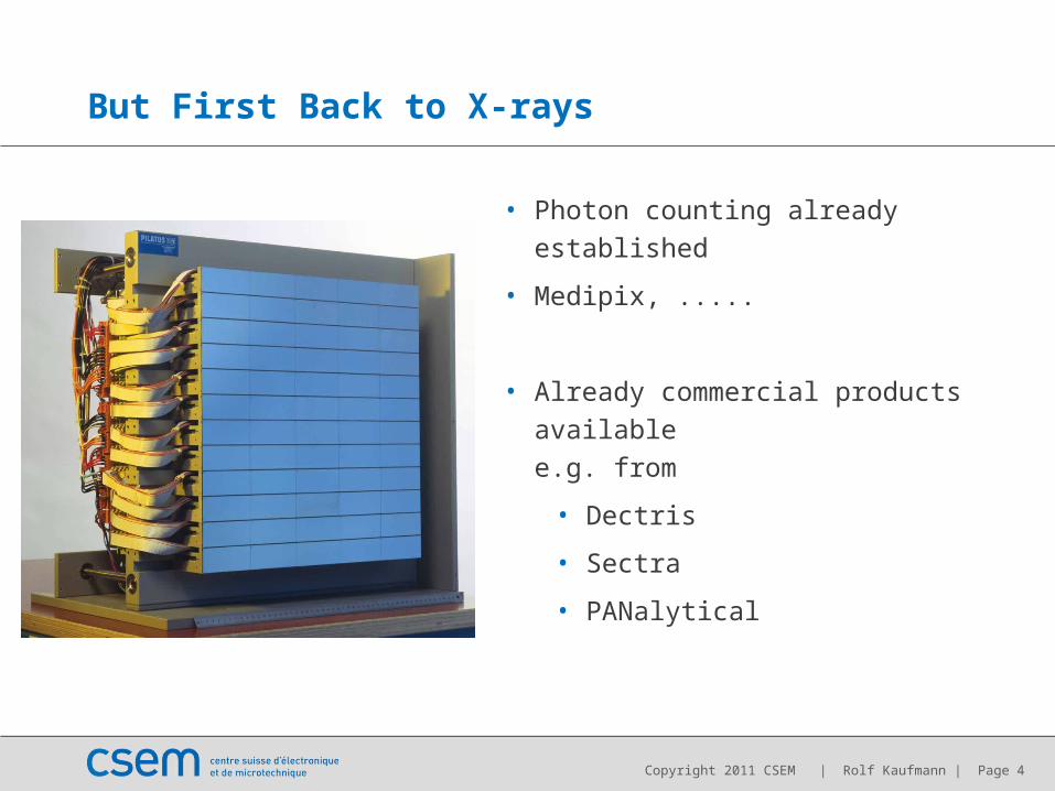
But First Back to X-rays
• Photon counting already established
• Medipix, .....
• Already commercial products available
e.g. from
• Dectris
• Sectra
• PANalytical
Copyright 2011 CSEM | Rolf Kaufmann | Page 5
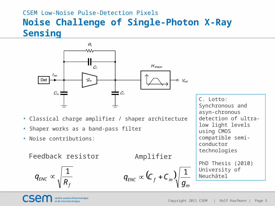
Noise Challenge of Single-Photon X-Ray Sensing
• Classical charge amplifier / shaper architecture
• Shaper works as a band-pass filter
• Noise contributions:
fENC Rq
1
Feedback resistor
m
infENC gCCq
1
Amplifier
C. Lotto: Synchronous and asyn-chronous detection of ultra-low light levels using CMOS compatible semi-conductor technologies
PhD Thesis (2010)University of Neuchâtel
CSEM Low-Noise Pulse-Detection Pixels

Copyright 2011 CSEM | Rolf Kaufmann | Page 6
Improved Band-Pass Filter
• High feed-back resistor Rr
• Low capacitances Cin and Cf
• Resistor implementations: MOS transistors in weak inversion
• Resitance approx. constant since no amplification between S/D
• Amplifier as a source follower (no Miller effect)
CSEM Low-Noise Pulse-Detection Pixels
Cs
Rr
sense node
1

Copyright 2011 CSEM | Rolf Kaufmann | Page 7
Transistor Level Circuit
CSEM Low-Noise Pulse-Detection Pixels
Clp
Cs
Chpgmlp
Vbias
RhpRr
rENC Rq
1
Feedback resistor
lphpsENC CandCCq
1
Amplifier

Copyright 2011 CSEM | Rolf Kaufmann | Page 8
Low-Noise Pulse-Detection Pixel Design Parameters
Parameter #1: Short Pulses #2: Long Pulses
Detected pulse width 1.5 ns – 10 ns 150 ns – 1.5 µs
Conversion factor 12.5uV/e- 27µV/e-
Recharge time constant 50 ns 10 µs
High-pass filter time constant 12 ns 2 µs
Pixel area 30 µm x 22 µm 30 µm x 20 µm
Fill factor 51 % 56 %
High-pass filtering capacitance 115 fF 200 fF
CSEM Low-Noise Pulse-Detection Pixels

Copyright 2011 CSEM | Rolf Kaufmann | Page 9
Noise Comparison Circuit Only (Simulation)
Circuit Component ENC contribution
Buffer 1.6 e
High pass filter 3.9 e
Low pass filter 1.4 e
Reset resistor 12.7 e
TOTAL 13.5 e
CSEM Low-Noise Pulse-Detection Pixels

Copyright 2011 CSEM | Rolf Kaufmann | Page 10
Photogate-Pixel to Reduce Sense-Node Capacitance

Copyright 2011 CSEM | Rolf Kaufmann | Page 11
Layout Example
30um
20umFF: 56%
Photogate with a smallSense node
CSEM Low-Noise Pulse-Detection Pixels

Copyright 2011 CSEM | Rolf Kaufmann | Page 12
Measurement Results
• Pulsed light of visible
wavelength
• Pulse width = 1us
• Repetition rate = 5000 Hz
CSEM Low-Noise Pulse-Detection Pixels
Copyright 2011 CSEM | Rolf Kaufmann | Page 13
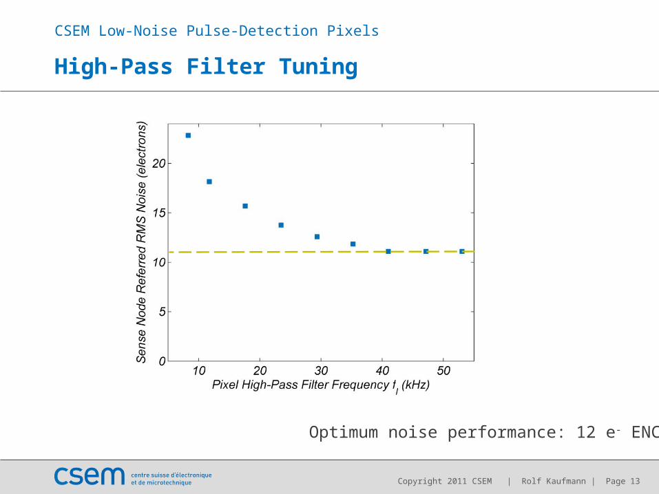
High-Pass Filter Tuning
Optimum noise performance: 12 e- ENC
CSEM Low-Noise Pulse-Detection Pixels

Copyright 2011 CSEM | Rolf Kaufmann | Page 14
Option: Scintillator based Pulse Detection Pixel
• Structured Scintillator to guide light onto one pixel
• Concept: Filling of trenches in Silicon wafer with scintillator material
• Minimal cross-talk between different pixels
• Low threshold (low noise) pulse detecting pixel required
scintillatorsilicon

Copyright 2011 CSEM | Rolf Kaufmann | Page 15
Monolithic Direct X-ray Detectors
• Germanium as detector material

Copyright 2011 CSEM | Rolf Kaufmann | Page 16
Monolithic Direct X-ray Detectors
• Ge epitaxially grown
on backside of
CMOS wafer
Monolithically integrated
direct detector
Challenges:
o Compatible CMOS process tungsten metallisation, n-type wafer
o Epitaxial growth of thick hetero-layers LEPECVD
n- Si
1 Pixel
n+p+
- HV
depletedarea
electricfieldlines
CMOS circuit
X-ray
p- Ge
e h
Copyright 2011 CSEM | Rolf Kaufmann | Page 17
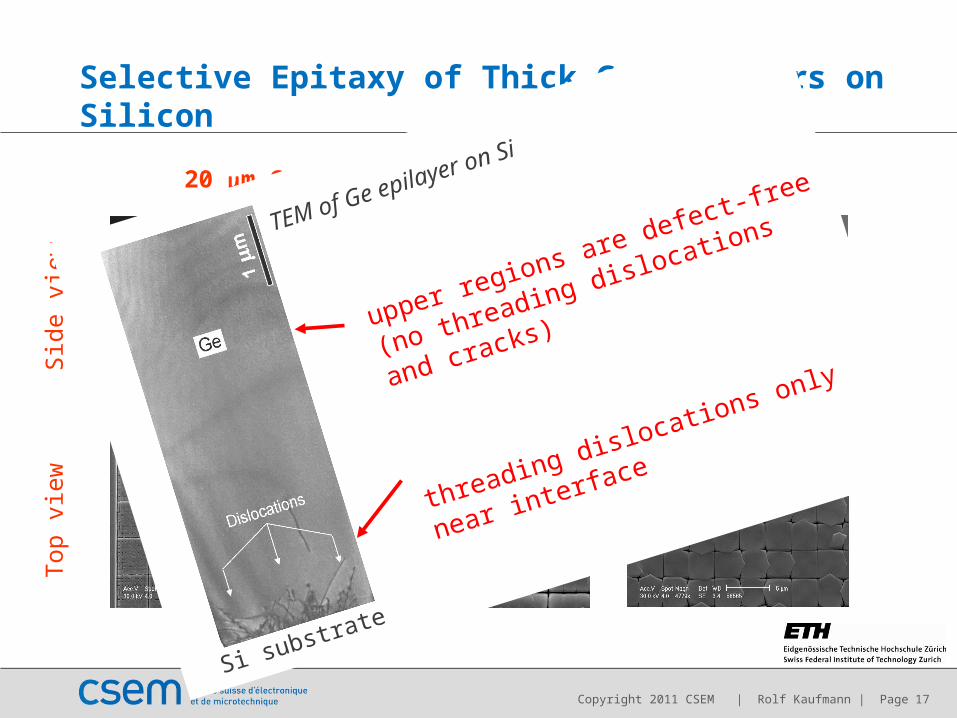
Selective Epitaxy of Thick Ge Absorbers on Silicon
20 m Ge pillars on Si (7.4 nm/s, 500 °C)
Top
vie
wS
ide
view
upper regions are defect-free
(no threading dislocations and cracks)
threading dislocations only near
interface
TEM of Ge epilayer on Si
Si substrate

Copyright 2011 CSEM | Rolf Kaufmann | Page 18
102030405060
10
20
30
40
50
60
0
100
200
300
400
500
NIR Ge Sensors
• Monolithic integration of
Ge photodetectors on CMOS
demonstrated for NIR application
• 64 x 64 pixel NIR image sensor exists
NIR detectors

Copyright 2011 CSEM | Rolf Kaufmann | Page 19
CSEM
… is under contract by the Swiss Government to perform
a special mission in micro- and nanotechnology
… has revenues (2009) of 70 MCHF, today ~ 400 employees,
five centers in Switzerland & international activities
… is a research and development company, active in
the domains of micro-, nano- and information technology
… is a private company, with mainly industrial, but also
public shareholders, not-for-profit
Centre Suisse d’Electronique et de Microtechnique

Copyright 2011 CSEM | Rolf Kaufmann | Page 20
CSEM – our mission
Technology transfer
Mission of CSEM
Mission of Universities
M A R K E T P U L L
T E C H N O L O G Y P U S H (Valorization)
MarketsEducation ResearchIndustrializationof Technologies
ProductDevelopment
Mission of Industries

Copyright 2011 CSEM | Rolf Kaufmann | Page 21
ZürichZürichBaselBasel
NeuchâtelNeuchâtel
AlpnachAlpnach LandquartLandquart
The CSEM Innovation Centers in Switzerland
Copyright 2011 CSEM | Rolf Kaufmann | Page 22
CSEM - PhotonicsTechnoparkstrasse 18005 ZurichSwitzerland

Copyright 2011 CSEM | Rolf Kaufmann | Page 23
Specialties and Competencies
• Optical systems in the VIS and NIR
• Image sensor desing
• Optical design
• Optical and electrical characterisation
• X-ray imaging
• Phase contrast x-ray
• X-ray detection
• Image processing software
• Integrated sensor systems
CSEM - Photonics

Copyright 2011 CSEM | Rolf Kaufmann | Page 24
Division Photonics
• 26 employees
• Mainly physicists and electro-engineers
• 2 PhD students
• International projects
• 1’100 m2 office, dark room
and lab space

Copyright 2011 CSEM | Rolf Kaufmann | Page 25
How to Implement Single Photon Detection in Visible Domain ?
• Extremely low noise levels necessary for
photon resolution (< 1electron ENC)
• Today’s image sensors use mostly
integrating and not pulse counting circuits
(except SiPM / APD arrays)
• Two architectures prevalent today:

Copyright 2011 CSEM | Rolf Kaufmann | Page 26
Charge Coupled Devices (CCD)
• Charge “buckets” implemented
as MOS capacitors
• Charge transport almost
noise free
• Noise from
• Leakage currents (~10 e/pixel/s)
can be reduced by cooling
• Read-out (<10 e/pixel/s)
good transistors difficult
to implement in CCD process
• CCD market shrinking for cost reasons

Copyright 2011 CSEM | Rolf Kaufmann | Page 27
Active Pixel Sensors
• CMOS APS
• CMOS NWELL as
photodiode
• At least 3 transistors
• Global shutter (snapshot)
possible with shutter transistor
• Still the usual circuit
architecture in image sensors
Copyright 2011 CSEM | Rolf Kaufmann | Page 28
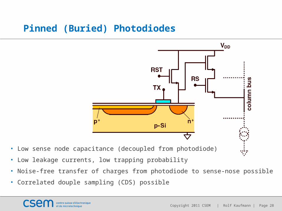
Pinned (Buried) Photodiodes
• Low sense node capacitance (decoupled from photodiode)
• Low leakage currents, low trapping probability
• Noise-free transfer of charges from photodiode to sense-nose possible
• Correlated douple sampling (CDS) possible

Copyright 2011 CSEM | Rolf Kaufmann | Page 29
Correlated Double Sampling (CDS)
• Thermal noise in reset transistors causes variations
of reset voltage
• KTC noise
• CDS sequence
1. Photoelectron integration (PPD)
2. Sense node reset
3. Readout of reset voltage
4. Transfer of photoelectrons
5. Readout of signal voltage
senseresetENC kTCq ,
Copyright 2011 CSEM | Rolf Kaufmann | Page 30
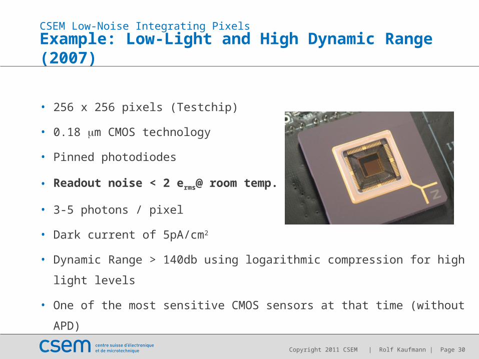
Example: Low-Light and High Dynamic Range (2007)
• 256 x 256 pixels (Testchip)
• 0.18 m CMOS technology
• Pinned photodiodes
• Readout noise < 2 erms@ room temp.
• 3-5 photons / pixel
• Dark current of 5pA/cm2
• Dynamic Range > 140db using logarithmic compression for high light levels
• One of the most sensitive CMOS sensors at that time (without APD)
CSEM Low-Noise Integrating Pixels

Copyright 2011 CSEM | Rolf Kaufmann | Page 31
Readout Noise in Integrating CMOS Image Sensors
• Image sensors with pinned photodiodes (PPD) and CDS (Correlated Double
Sampling): Readout noise can be dominant sensor noise source
• Readout noise in conventional image sensors:
CSEM Low-Noise Integrating Pixels
sense node
colu
mn
line
reset
transfer
select
biasADC
• Source-follower noise: ENC
proportional to sense-node
capacitance => PPD ideal !
• High impact of downstream
circuit noise due to low pixel
conversion factor

Copyright 2011 CSEM | Rolf Kaufmann | Page 32
Amplifying Pixel
Limit bandwidth & reduced impact of downstream circuit noise
CSEM Low-Noise Integrating Pixels
Conventional
e
VC
qCF
sensepixel
sense nodeco
lum
nlin
e
reset
transfer
select
bias
columnsensethermalENC kTCCq ,
Amplifying pixel
sensevpixel C
qACF
sense node
reset_n
transfer
select_n
colu
mn
line
Rl
columnvsensethermalENC CAkTCq ,

Copyright 2011 CSEM | Rolf Kaufmann | Page 33
Reset Switch
• Reset switch on: reset voltage senses column offset voltage differences
• Guarantees a constant amplifier operating point
Conventional Amplifying pixel
sense node
colu
mn
line
reset
transfer
select
bias
sense node
reset_n
transfer
select_n
colu
mn
line
Rl
CSEM Low-Noise Integrating Pixels

Copyright 2011 CSEM | Rolf Kaufmann | Page 34
Amplifying Pixel Measurement Results
Parameter Value
Pixel pitch 11µm
Fill factor 40% to 48%
Transistor count 4
Sense node capacitance 5.3 fF
Voltage gain (linear) 9.9
Pixel conversion factor (linear) 300µV/e-
Linear range 3 ke-
Full well capacity 34 ke-
Dynamic range (Texp = 17ms) 87.1dB
CSEM Low-Noise Integrating Pixels
C. Lotto: Synchronous and asyn-chronous detection of ultra-low light levels using CMOS compatible semi-conductor technologies
PhD Thesis (2010)University of Neuchâtel

Copyright 2011 CSEM | Rolf Kaufmann | Page 35
Noise Measurements
• Readout noise: sequence without activation of TX gate
• Dark noise:
Readout noise + Photodiode dark current shot noise + Transfer noise
Readout noise:
0.9 electrons
Dark noise (Texp=17ms):
1.5 electrons
CSEM Low-Noise Integrating Pixels
Copyright 2011 CSEM | Rolf Kaufmann | Page 36
Conclusions
• Visible light image sensors are close to single photon detection capability
• In-pixel amplification including optimized bandwidth engineering
• Sub-electron readout noise at practical pixel pitch, fill factor, frame rate and dynamic range
• X-ray pulse detection pixels also benefit from low noise circuits
• In-pixel band-pass filtering
• Overall noise floor of 12 electrons

Thank you for your attention.