single-stage ac/dc dual inductor bcm current-fed push-pull ... · energy efficiency and low...
TRANSCRIPT
Single-stage AC/DC Dual Inductor BCM Current-Fed
Push-Pull for HB-LED lighting applications
Ignacio Castro, Kevin Martin, Diego G. Lamar, Manuel Arias, Marta M. Hernando and Javier Sebastian Departamento de Ingeniería Eléctrica, Electrónica, de Computadores y Sistemas
University of Oviedo
Gijón 33204, Spain e-mail: [email protected]
Abstract— A single-stage, AC/DC driver for High Brightness
Light-Emitting Diodes (HB-LED) with galvanic isolation is
presented in this paper. The driver is based on a Dual Inductor
Current-fed Push-Pull (DICPP) converter with each inductor
operating in Boundary Conduction Mode (BCM). The
interleaving between the two inductors makes possible for the
converter to reduce the high input current ripple of a BCM.
Moreover, it is fully compliant with IEC 1000-3-2 Class C, and it
is also able to achieve high Power Factor (PF). Moreover, the low
component count, simplicity and overall outstanding
characteristics make this topology suitable for medium power
range HB-LED drivers in low cost applications.
Finally, the proposed topology has been tested on a 90W
prototype for the full range of the US single-phase line voltage,
feeding several strings of HB-LED, with an output voltage of 48V
at full load. The prototype achieves a maximum efficiency of 92%
with 0.99 power factor, 8% THD at full load and guarantees good
quality light.
Keywords—Single phase, Ac-dc power conversion, Power Factor
Correction, HB-LED driver
I. INTRODUCTION
High-Brightness Light-Emitting Diodes (HB-LED) are increasingly becoming the main source of artificial light in our homes, offices and streets due to their reliability, long life, energy efficiency and low maintenance requirements. However, the driving of HB-LED with primary access to single phase AC requires the use of a converter that achieves high efficiency, Power Factor Correction (PFC) in order to comply with the regulation for both residential and commercial lighting and a long lifespan comparable to that of the HB-LEDs. High Power Factor (PF) is required to maximize the power transferred by the grid. Energy Star® [1], requires 0.7 PF for residential lighting and 0.9 PF for commercial lighting. Furthermore, the low-frequency harmonic content of the line current, must comply with IEC 1000-3-2 Class C [2]-[4], which establishes very strict harmonic content for the line current, for lighting equipment of more than 25 W. Therefore, the line current needs to have a sinusoidal shape following that of the input voltage. Traditionally, HB-LED drivers are based on a high-performance AC/DC PFC converter, followed by a dc-dc converter (in most situations with galvanic isolation), that provides constant current to the HB-LED, in order to comply with the aforementioned regulation.
Nonetheless, in most scenarios, the cost of the HB-LED driver is the main concern and a single-stage has to be used,
especially in medium power range HB-LED drivers, where galvanic isolation is recommended for safety requirements. For that reason, isolated buck-boost topologies, like the flyback working in Discontinuous Conduction Mode (DCM), which achieve unity PF naturally are widely used [5]-[7]. Although, these topologies have a low component count, they suffer from having low efficiencies (<90%) and the inability to remove the bulk capacitor needed in PFC. Nevertheless, the removal of the bulk capacitor is not always possible in a single-stage without including more active components [8]-[11] or distorting the input current [12] [13] due to the pulsating input power of the grid.
Another topology that is able to achieve unity PF naturally, by means of control, is the boost converter. The boost converter is normally used as a front-end AC/DC PFC converter operating either in Boundary Conduction Mode (BCM) or with a Multiplier-Based Control (MBC) [14] [15] with a cascaded step-down converter normally with galvanic isolation. The isolated variations of the boost family converters are suitable to be used in a single-stage PFC. It should be noted that current-fed based isolated converters have some issues, such as, having a complex transformer design or having the need of a demagnetizing path for the main inductance, as has been stated in previous literature [16].
Nevertheless, in previous literature, there have been some works dedicated to single-stage AC/DC PFC current-fed based isolated converters, such as the push-pull [17] or the full-bridge [18]. These topologies are based in the boost converter, hence they can achieve unity PF by working in BCM. However, BCM has an important drawback regarding the size increase of the EMI filter due to the high input current ripple and the variable frequency, which can be reduced by interleaving two or more boost converters in parallel [19]. Therefore, the interleaving of two isolated boosts can reduce the input current ripple of the
This work has been supported by the Spanish Government under Project
MINECO-13-DPI2013-47176-C2-2-R and the Principality of Asturias under the grants “Severo Ochoa” BP14-140 and BP14-85 and by the Project FC-15-
GRUPIN14-143 and by European Regional Development Fund (ERDF) grants.
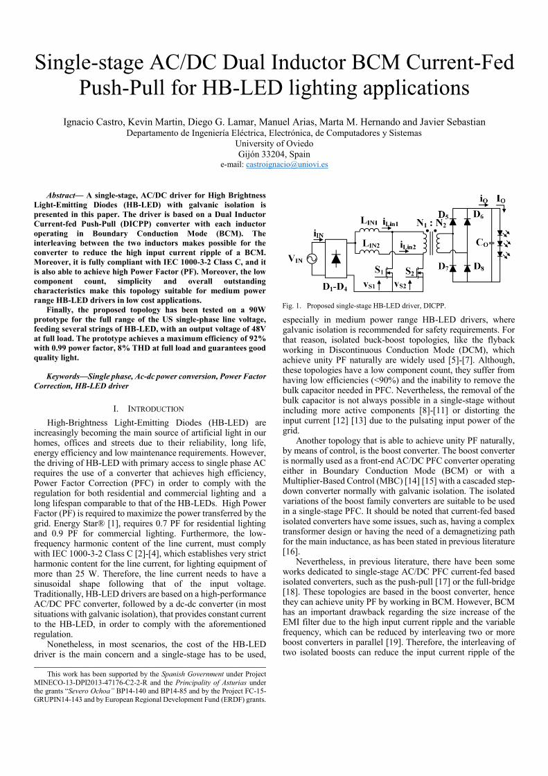
Fig. 1. Proposed single-stage HB-LED driver, DICPP.
converter, as stated in [20]. However, this topology requires four MOSFET, whereas the Dual Inductor Current-fed Push-Pull (DICPP) (see Fig. 1) proposed in [21], [22] achieves the same input current reduction with the use of only two MOSFET and only one transformer. The DICPP uses the same amount of switches when compared to the classic Current-fed Push-Pull (CPP) [22], and the transformer is a one winding to one winding which is simpler to design and build than the classic CPP transformer. This is particularly important to reduce the parasitic components that may cause an inadequate behaviour of the topology due to resonances in the output current or the losses in the passive snubbers that will decrease the efficiency of the single-stage.
Hence, this work proposes the optimization of the DICPP and enhances the scope of the topology in order to make it suitable for PFC with a simple control method. The operation in BCM makes the DICPP as a plausible solution for single-stage PFC in HB-LED drivers, which reduces the size of the EMI filter when compared to other topologies working in BCM and achieves high efficiency (92%). However, it is not able to eliminate the classic bulk capacitor in PFC if a non-flicker behaviour needs to be guaranteed on the HB-LEDs. In that sense a high efficiency post-regulator stage can be used to remove the bulk capacitor and to individually control each HB-LED string[X].
This work is divided in several section: Section II, will analyze the proposed topology, as well as, discuss the most important features of the proposed driver with a dedicated subsection for the transformer and inductor design. Section III, will be dedicated to the most representative experimental results that were obtained with the proposed driver.
II. WORKING PRINCIPLE
A. Static Analysis
The concept of the HB-LED driver presented in this work (i.e. DICPP) is based on [21], where it was proposed as a dc-dc converter working in CCM. Hence, this paper proposes to increase the scope of the topology to work as a PFC. The CPP converter is equivalent to a boost converter with galvanic isolation.
In order to achieve good quality rectification in the input current, a Loss Free Resistor (LFR) [23] behaviour is required. It is well known that a boost converter operating in BCM can achieve a LFR behaviour naturally. Therefore, the DICPP should also be able to achieve PFC naturally by working in BCM.
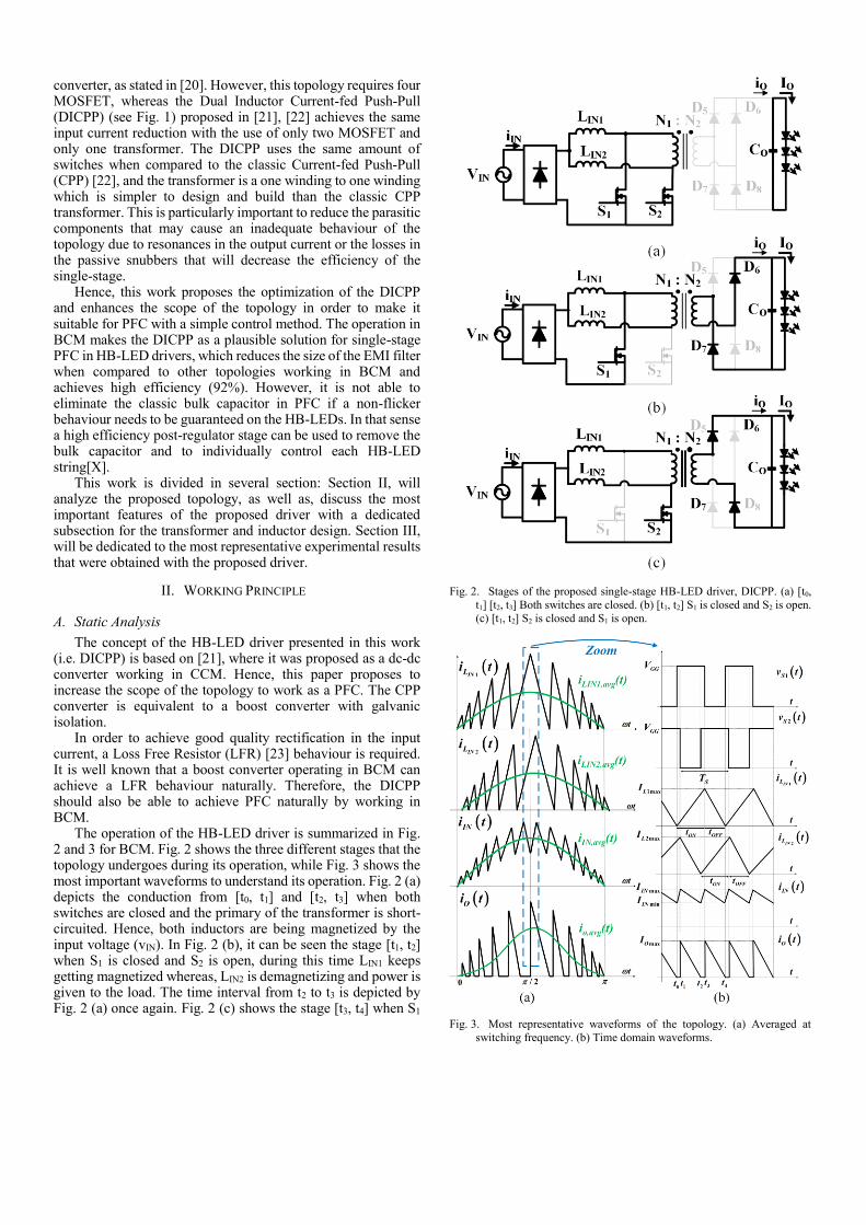
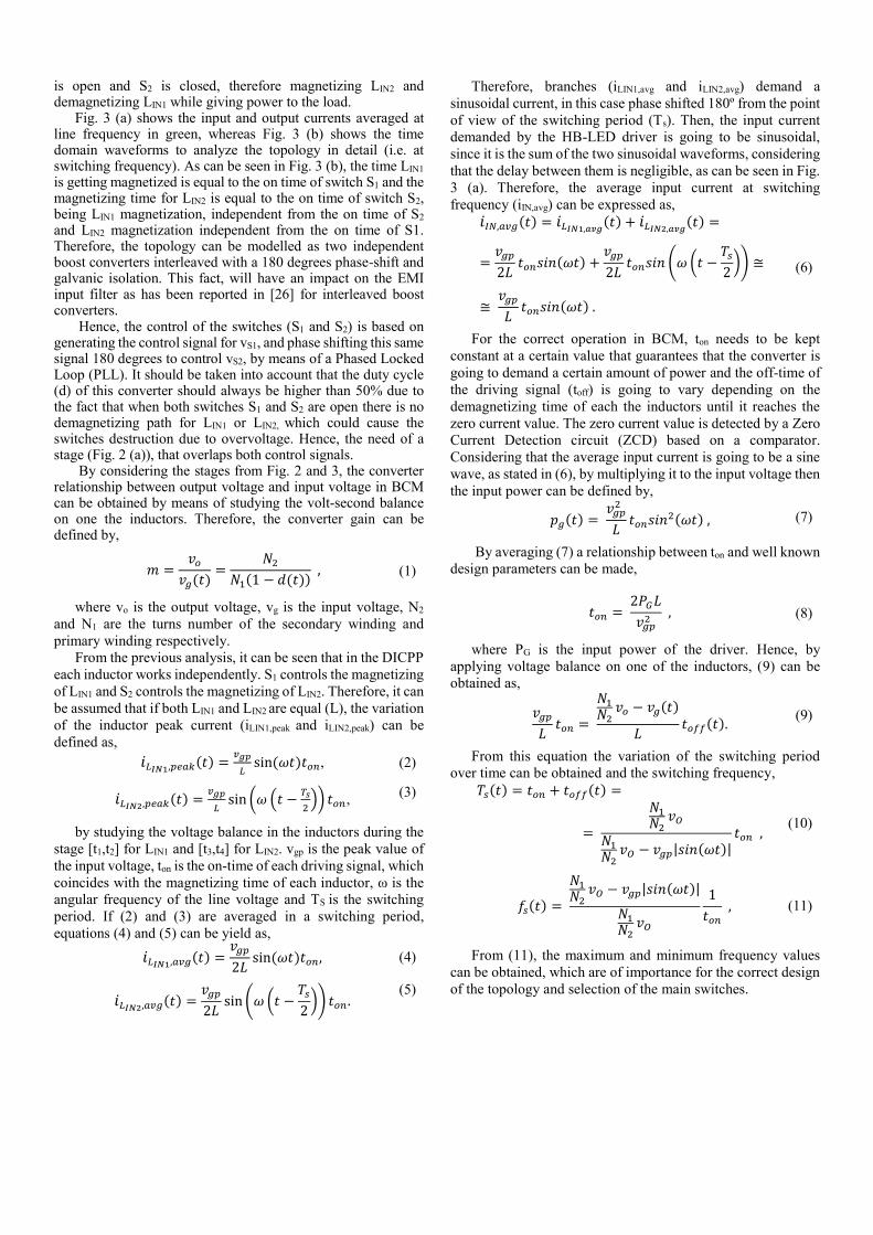
The operation of the HB-LED driver is summarized in Fig. 2 and 3 for BCM. Fig. 2 shows the three different stages that the topology undergoes during its operation, while Fig. 3 shows the most important waveforms to understand its operation. Fig. 2 (a) depicts the conduction from [t0, t1] and [t2, t3] when both switches are closed and the primary of the transformer is short-circuited. Hence, both inductors are being magnetized by the input voltage (vIN). In Fig. 2 (b), it can be seen the stage [t1, t2] when S1 is closed and S2 is open, during this time LIN1 keeps getting magnetized whereas, LIN2 is demagnetizing and power is given to the load. The time interval from t2 to t3 is depicted by Fig. 2 (a) once again. Fig. 2 (c) shows the stage [t3, t4] when S1
Fig. 3. Most representative waveforms of the topology. (a) Averaged at
switching frequency. (b) Time domain waveforms.
Fig. 2. Stages of the proposed single-stage HB-LED driver, DICPP. (a) [t0,
t1] [t2, t3] Both switches are closed. (b) [t1, t2] S1 is closed and S2 is open.
(c) [t1, t2] S2 is closed and S1 is open.
S1
is open and S2 is closed, therefore magnetizing LIN2 and demagnetizing LIN1 while giving power to the load.
Fig. 3 (a) shows the input and output currents averaged at line frequency in green, whereas Fig. 3 (b) shows the time domain waveforms to analyze the topology in detail (i.e. at switching frequency). As can be seen in Fig. 3 (b), the time LIN1 is getting magnetized is equal to the on time of switch S1 and the magnetizing time for LIN2 is equal to the on time of switch S2, being LIN1 magnetization, independent from the on time of S2 and LIN2 magnetization independent from the on time of S1. Therefore, the topology can be modelled as two independent boost converters interleaved with a 180 degrees phase-shift and galvanic isolation. This fact, will have an impact on the EMI input filter as has been reported in [26] for interleaved boost converters.
Hence, the control of the switches (S1 and S2) is based on generating the control signal for vS1, and phase shifting this same signal 180 degrees to control vS2, by means of a Phased Locked Loop (PLL). It should be taken into account that the duty cycle (d) of this converter should always be higher than 50% due to the fact that when both switches S1 and S2 are open there is no demagnetizing path for LIN1 or LIN2, which could cause the switches destruction due to overvoltage. Hence, the need of a stage (Fig. 2 (a)), that overlaps both control signals.
By considering the stages from Fig. 2 and 3, the converter relationship between output voltage and input voltage in BCM can be obtained by means of studying the volt-second balance on one the inductors. Therefore, the converter gain can be defined by,
𝑚 =𝑣𝑜
𝑣𝑔(𝑡)=
𝑁2
𝑁1(1 − 𝑑(𝑡)) , (1)
where vo is the output voltage, vg is the input voltage, N2
and N1 are the turns number of the secondary winding and
primary winding respectively.
From the previous analysis, it can be seen that in the DICPP
each inductor works independently. S1 controls the magnetizing
of LIN1 and S2 controls the magnetizing of LIN2. Therefore, it can
be assumed that if both LIN1 and LIN2 are equal (L), the variation
of the inductor peak current (iLIN1,peak and iLIN2,peak) can be
defined as,
𝑖𝐿𝐼𝑁1,𝑝𝑒𝑎𝑘(𝑡) =𝑣𝑔𝑝
𝐿sin (𝜔𝑡)𝑡𝑜𝑛, (2)
𝑖𝐿𝐼𝑁2,𝑝𝑒𝑎𝑘(𝑡) =𝑣𝑔𝑝
𝐿sin (𝜔 (𝑡 −
𝑇𝑠
2)) 𝑡𝑜𝑛,
(3)
by studying the voltage balance in the inductors during the
stage [t1,t2] for LIN1 and [t3,t4] for LIN2. vgp is the peak value of
the input voltage, ton is the on-time of each driving signal, which
coincides with the magnetizing time of each inductor, ω is the
angular frequency of the line voltage and TS is the switching
period. If (2) and (3) are averaged in a switching period,
equations (4) and (5) can be yield as,
𝑖𝐿𝐼𝑁1,𝑎𝑣𝑔(𝑡) =𝑣𝑔𝑝
2𝐿sin (𝜔𝑡)𝑡𝑜𝑛, (4)
𝑖𝐿𝐼𝑁2,𝑎𝑣𝑔(𝑡) =
𝑣𝑔𝑝
2𝐿sin (𝜔 (𝑡 −
𝑇𝑠
2)) 𝑡𝑜𝑛 .
(5)
Therefore, branches (iLIN1,avg and iLIN2,avg) demand a
sinusoidal current, in this case phase shifted 180º from the point
of view of the switching period (Ts). Then, the input current
demanded by the HB-LED driver is going to be sinusoidal,
since it is the sum of the two sinusoidal waveforms, considering
that the delay between them is negligible, as can be seen in Fig.
3 (a). Therefore, the average input current at switching
frequency (iIN,avg) can be expressed as,
𝑖𝐼𝑁,𝑎𝑣𝑔(𝑡) = 𝑖𝐿𝐼𝑁1,𝑎𝑣𝑔(𝑡) + 𝑖𝐿𝐼𝑁2,𝑎𝑣𝑔
(𝑡) =
=𝑣𝑔𝑝
2𝐿𝑡𝑜𝑛𝑠𝑖𝑛(𝜔𝑡) +
𝑣𝑔𝑝
2𝐿𝑡𝑜𝑛𝑠𝑖𝑛 (𝜔 (𝑡 −
𝑇𝑠
2)) ≅
≅ 𝑣𝑔𝑝
𝐿𝑡𝑜𝑛𝑠𝑖𝑛(𝜔𝑡) .
(6)
For the correct operation in BCM, ton needs to be kept
constant at a certain value that guarantees that the converter is
going to demand a certain amount of power and the off-time of
the driving signal (toff) is going to vary depending on the
demagnetizing time of each the inductors until it reaches the
zero current value. The zero current value is detected by a Zero
Current Detection circuit (ZCD) based on a comparator.
Considering that the average input current is going to be a sine
wave, as stated in (6), by multiplying it to the input voltage then
the input power can be defined by,
𝑝𝑔(𝑡) = 𝑣𝑔𝑝
2
𝐿𝑡𝑜𝑛𝑠𝑖𝑛2(𝜔𝑡) , (7)
By averaging (7) a relationship between ton and well known
design parameters can be made,
𝑡𝑜𝑛 = 2𝑃𝐺𝐿
𝑣𝑔𝑝2
, (8)
where PG is the input power of the driver. Hence, by
applying voltage balance on one of the inductors, (9) can be
obtained as,
𝑣𝑔𝑝
𝐿𝑡𝑜𝑛 =
𝑁1
𝑁2𝑣𝑜 − 𝑣𝑔(𝑡)
𝐿𝑡𝑜𝑓𝑓(𝑡).
(9)
From this equation the variation of the switching period
over time can be obtained and the switching frequency,
𝑇𝑠(𝑡) = 𝑡𝑜𝑛 + 𝑡𝑜𝑓𝑓(𝑡) =
=
𝑁1
𝑁2𝑣𝑂
𝑁1
𝑁2𝑣𝑂 − 𝑣𝑔𝑝|𝑠𝑖𝑛(𝜔𝑡)|
𝑡𝑜𝑛 , (10)
𝑓𝑠(𝑡) =
𝑁1
𝑁2𝑣𝑂 − 𝑣𝑔𝑝|𝑠𝑖𝑛(𝜔𝑡)|
𝑁1
𝑁2𝑣𝑂
1
𝑡𝑜𝑛
, (11)
From (11), the maximum and minimum frequency values
can be obtained, which are of importance for the correct design
of the topology and selection of the main switches.
B. Design Criteria of the HB-LED driver
In order to design the HB-LED driver correctly some steps
need to be followed.
First of all the transformer relation needs to be obtained
from (1), considering vgp as the maximum value of the input
voltage range (i.e. Vgpmax), vo as the output voltage at the full
dimming value and dmin as the minimum duty cycle acceptable,
which should be around 55%.
After obtaining the transformer relation, the duty cycle
needs to be calculated in nominal conditions, with that duty
cycle and the desired switching frequency is possible to
calculate the inductors required from (8). If the inductor value
is feasible, (11) should be used to check if the frequency range
is suitable. If not, then the inductance value needs to be adjusted
to suit the designer specifications. Guaranteeing that the lowest
frequency value is higher than 20 kHz is a good practice to
avoid any noise in the converter.
After having calculated all the previous parameters, the next
step would be to select the main switches. For that reason is
necessary to know the maximum current and voltage that they
are going to endure, from (1) and (7),
𝑉𝑆𝑚𝑎𝑥 =
𝑁1
𝑁2
𝑣𝑜 , (12)
𝐼𝑆𝑚𝑎𝑥 =
𝑃𝑔
𝑉𝑔𝑝𝑚𝑖𝑛
, (13)
where Vgpmin is the voltage peak of the minimum voltage in
the range. As can be seen, the maximum voltage is completely
reliant on the output voltage and the transformer relation.
Considering that the transformer turns ratio is calculated based
on the maximum input voltage, European/Universal range
would require the use of switches with a higher breakdown
voltage (i.e. 1200 V).
For the sake of selecting the high frequency diodes (D5-
D8), the maximum values that need to be taken into account are
shown,
𝑉𝐷𝑚𝑎𝑥 = 𝑉𝑜 −
𝑁2
𝑁1
𝑉𝑔𝑝𝑚𝑖𝑛 , (14)
𝐼𝐷𝑚𝑎𝑥 =
𝑁1
𝑁2
𝐼𝐿𝐼𝑁1,𝑝𝑒𝑎𝑘,𝑚𝑎𝑥 , (15)
where ILIN1,peak,max is the maximum input current of the HB-
LED driver. As it can be seen, the breakdown voltage of the
high frequency diode bridge can be low enough to guarantee the
use of very low knee-voltage diode in order to improve the
efficiency of the driver.
Finally, in order to be able to demagnetize both inductors in
case of having the need to shut down the HB-LED driver,
another winding is added to give a path for the demagnetization
to occur, as has been done in previous works [16][17]. Even though, it is not shown in Fig. 2, the HB-LED driver
also has a clamping snubber implemented to protect both switches from overvoltage.
C. Transformer design
In push-pull converters, where the current through the primary transformer winding is abruptly changed whenever a transistor switches, leakage inductance should be as low as possible. Otherwise, each switching instant would cause a significant voltage spike, making the use of higher voltage rated transistors or protective devices such as snubbers.
Winding interleaving is a well-known procedure for reducing the leakage inductance. However, as a side effect of adding a high number of thinner sub-windings, a really low leakage inductance can only be obtained at the cost of a high parasitic capacitance. This proved to be troublesome, when voltage spikes due to leakage inductance were close to non-existent but the transformer resonated due to stray capacitances similar to the transistor Coss. This recirculating currents not only increase the converter losses but also make the event detection for the control more difficult to implement, requiring complex filters.
This resonance has been studied in [27], where it is shown that both the leakage inductance and the stray capacitance play an important role. A low leakage inductance value is extremely important. A common target for a well-designed transformer is a leakage inductance at least thousand times lower than the transformer magnetizing inductance. The parasitic capacitor is nowhere as critical as a low leakage inductance. Nevertheless, it should be taken into account when designing the transformer.
Using planar magnetic technologies is a feasible option, whose main advantages are the ease of implementation of interleaved windings and the predictability and repeatability of the process [28]. However, in order to attain a low leakage inductance, a high amount of PCB layers are needed, rapidly increasing both its cost and the winding capacitance. Although some techniques have been presented in order to reduce parasitic capacitance in planar transformers [28] [29], for this paper a simpler, traditional transformer is designed.
Based on the previously shown design equations and specifications, an 11:1 transformer is designed aiming for low losses in a quite wide frequency range around 150 kHz. Its magnetizing inductance is not critical as long as it is much higher than LIN1 and LIN2. An EPCOS RM12 – N49 core is chosen for being compact and adequate to the design requirements. Several designs were simulated using ANSYS® Maxwell and PExprt.
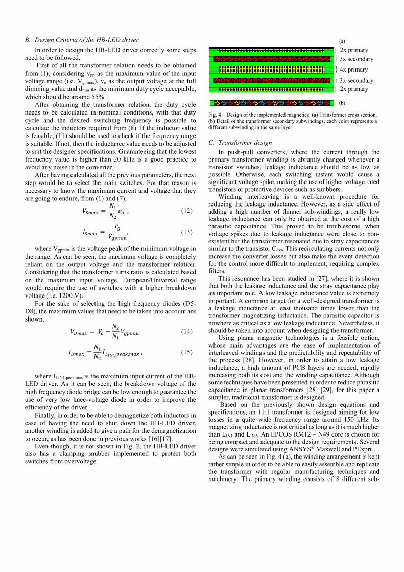
As can be seen in Fig. 4 (a), the winding arrangement is kept rather simple in order to be able to easily assemble and replicate the transformer with regular manufacturing techniques and machinery. The primary winding consists of 8 different sub-
Fig. 4. Design of the implemented magnetics. (a) Transformer cross section.
(b) Detail of the transformer secondary subwindings, each color represents a
different subwinding in the same layer.
(a)
(b)
} 2x primary
} 3x secondary
4x primary
} 3x secondary
} 2x primary
windings of 66 turns of AWG 35 copper wire, all connected in parallel.
The secondary winding consists of 6 different sub-windings of 6 turns. They are arranged in only two layers, interleaved with the primary, of three windings each. It is important to note, that each winding is built from Litz wire comprising 10 AWG 35 wires. This way, the total thickness is small enough to evenly spread the windings along the window height, thus reducing the leakage inductance even more. If a single, thicker winding was used on each layer, it would not fit the available winding area.
Different implementation options were also considered for the secondary winding. The use of copper foil is an interesting alternative, but the benefit does not justify the increase of the manufacturing difficulty, requiring custom foil thicknesses or even laser cutting for fitting the required turns in just one layer. Simulations did not show significant advantages over the preferred, simple designs, so this approach was discarded.
As the copper windings do not completely fill the winding area, PET insulating tape layers are added between them. This serves a dual purpose: fixing and insulating the primary and secondary layers and creating wider spaces between them, lowering the stray capacitance.
Table I shows the maximum target parasitic values for the desired transformer design, the values obtained for different implementations using Finite Element Analysis (FEA) simulations and the actual measurements from the implemented interleaved transformer. It can be seen that the not interleaved design does not comply with the desired specifications and the foil-based transformer provides a much lower leakage inductance at the cost of a highly increased assembly complexity. The interleaved transformer is easy enough to manufacture and fulfills the desired specifications.
The design of the input inductors is not as critical as that of the transformer, but a custom design is also used for this prototype. There is a wide range of commercial inductors which fulfill the inductance and frequency requirements with small form factors but high losses. An EPCOS RM8 – N97 core is chosen, with two AWG 29, 22-turn windings connected in parallel. The obtained design is only slightly bigger than equivalent commercial inductances but cut conduction losses by more than half.
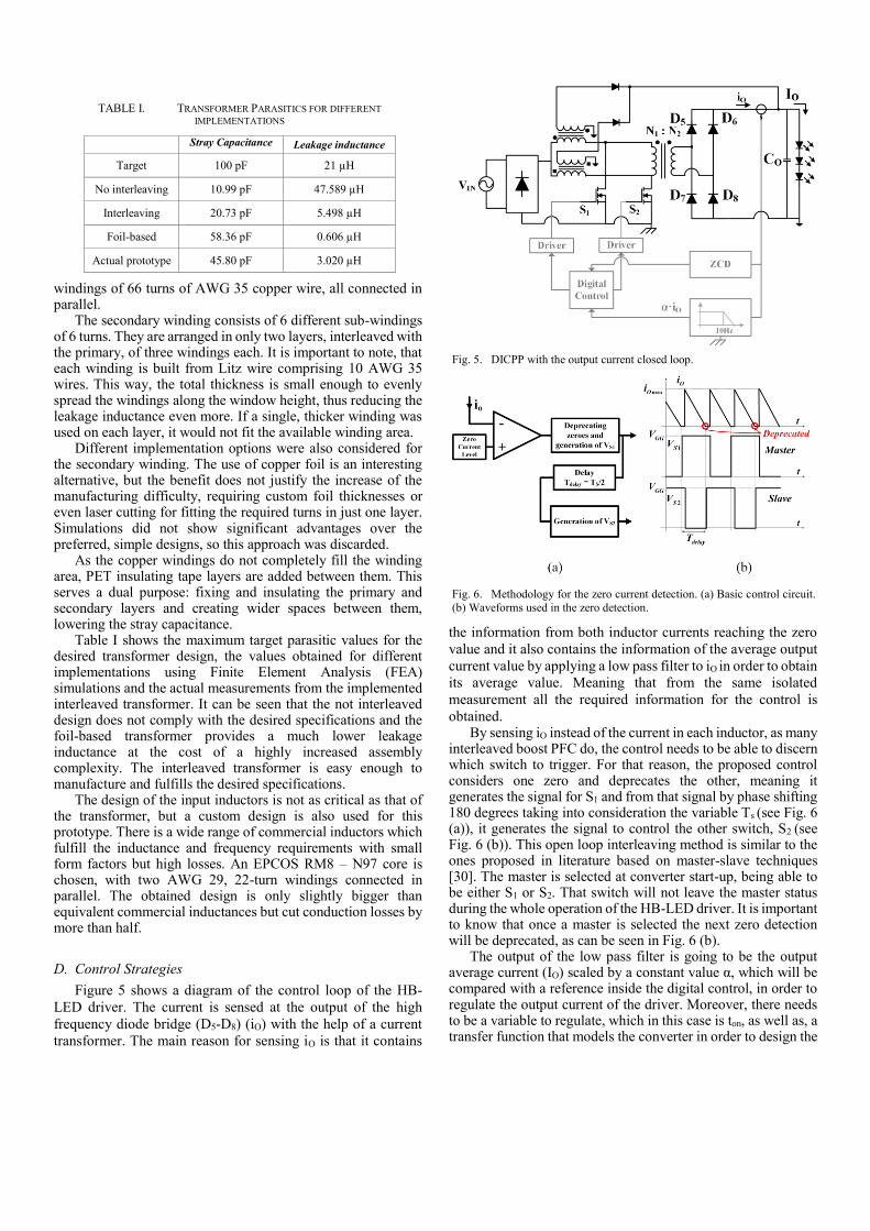
D. Control Strategies
Figure 5 shows a diagram of the control loop of the HB-
LED driver. The current is sensed at the output of the high
frequency diode bridge (D5-D8) (iO) with the help of a current
transformer. The main reason for sensing iO is that it contains
the information from both inductor currents reaching the zero
value and it also contains the information of the average output
current value by applying a low pass filter to iO in order to obtain
its average value. Meaning that from the same isolated
measurement all the required information for the control is
obtained. By sensing iO instead of the current in each inductor, as many
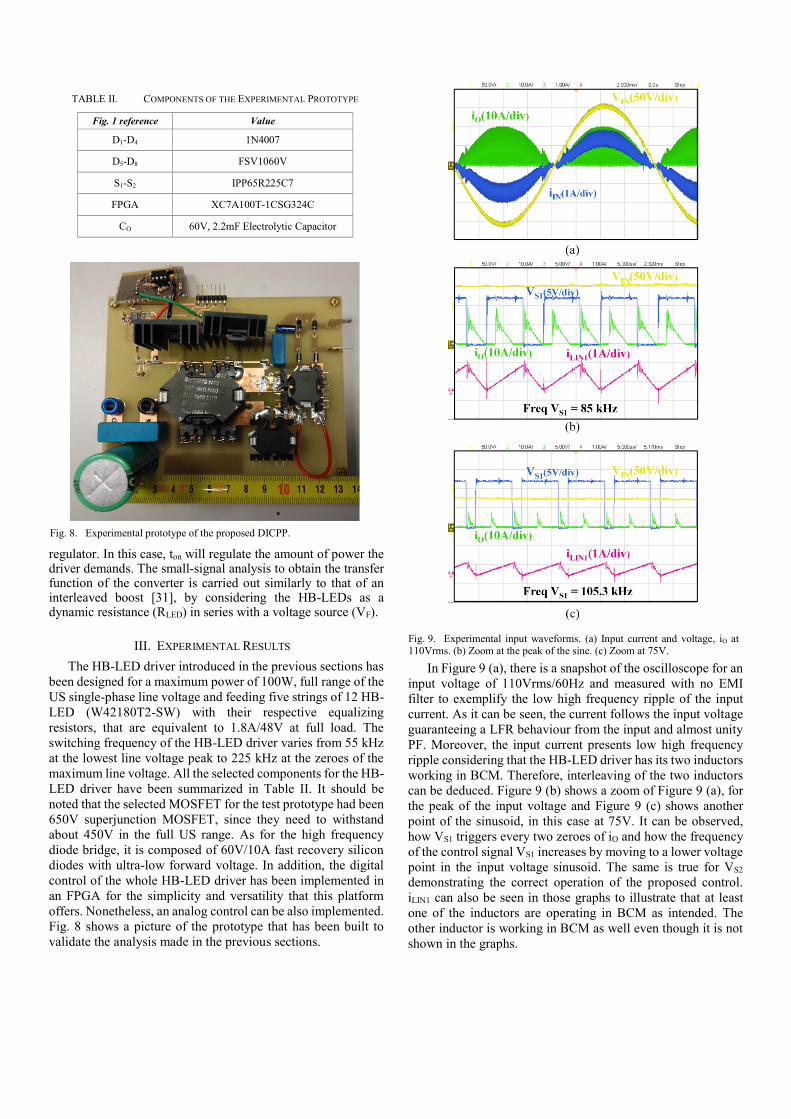
interleaved boost PFC do, the control needs to be able to discern which switch to trigger. For that reason, the proposed control considers one zero and deprecates the other, meaning it generates the signal for S1 and from that signal by phase shifting 180 degrees taking into consideration the variable Ts (see Fig. 6 (a)), it generates the signal to control the other switch, S2 (see Fig. 6 (b)). This open loop interleaving method is similar to the ones proposed in literature based on master-slave techniques [30]. The master is selected at converter start-up, being able to be either S1 or S2. That switch will not leave the master status during the whole operation of the HB-LED driver. It is important to know that once a master is selected the next zero detection will be deprecated, as can be seen in Fig. 6 (b).
The output of the low pass filter is going to be the output average current (IO) scaled by a constant value α, which will be compared with a reference inside the digital control, in order to regulate the output current of the driver. Moreover, there needs to be a variable to regulate, which in this case is ton, as well as, a transfer function that models the converter in order to design the
Fig. 6. Methodology for the zero current detection. (a) Basic control circuit.
(b) Waveforms used in the zero detection.
Fig. 5. DICPP with the output current closed loop.
TABLE I. TRANSFORMER PARASITICS FOR DIFFERENT
IMPLEMENTATIONS
Stray Capacitance Leakage inductance
Target 100 pF 21 µH
No interleaving 10.99 pF 47.589 µH
Interleaving 20.73 pF 5.498 µH
Foil-based 58.36 pF 0.606 µH
Actual prototype 45.80 pF 3.020 µH
regulator. In this case, ton will regulate the amount of power the driver demands. The small-signal analysis to obtain the transfer function of the converter is carried out similarly to that of an interleaved boost [31], by considering the HB-LEDs as a dynamic resistance (RLED) in series with a voltage source (VF).
III. EXPERIMENTAL RESULTS
The HB-LED driver introduced in the previous sections has
been designed for a maximum power of 100W, full range of the
US single-phase line voltage and feeding five strings of 12 HB-
LED (W42180T2-SW) with their respective equalizing
resistors, that are equivalent to 1.8A/48V at full load. The
switching frequency of the HB-LED driver varies from 55 kHz
at the lowest line voltage peak to 225 kHz at the zeroes of the
maximum line voltage. All the selected components for the HB-
LED driver have been summarized in Table II. It should be
noted that the selected MOSFET for the test prototype had been
650V superjunction MOSFET, since they need to withstand
about 450V in the full US range. As for the high frequency
diode bridge, it is composed of 60V/10A fast recovery silicon
diodes with ultra-low forward voltage. In addition, the digital
control of the whole HB-LED driver has been implemented in
an FPGA for the simplicity and versatility that this platform
offers. Nonetheless, an analog control can be also implemented.
Fig. 8 shows a picture of the prototype that has been built to
validate the analysis made in the previous sections.
In Figure 9 (a), there is a snapshot of the oscilloscope for an
input voltage of 110Vrms/60Hz and measured with no EMI
filter to exemplify the low high frequency ripple of the input
current. As it can be seen, the current follows the input voltage
guaranteeing a LFR behaviour from the input and almost unity
PF. Moreover, the input current presents low high frequency
ripple considering that the HB-LED driver has its two inductors
working in BCM. Therefore, interleaving of the two inductors
can be deduced. Figure 9 (b) shows a zoom of Figure 9 (a), for
the peak of the input voltage and Figure 9 (c) shows another
point of the sinusoid, in this case at 75V. It can be observed,
how VS1 triggers every two zeroes of iO and how the frequency
of the control signal VS1 increases by moving to a lower voltage
point in the input voltage sinusoid. The same is true for VS2
demonstrating the correct operation of the proposed control.
iLIN1 can also be seen in those graphs to illustrate that at least
one of the inductors are operating in BCM as intended. The
other inductor is working in BCM as well even though it is not
shown in the graphs.
Fig. 8. Experimental prototype of the proposed DICPP.
TABLE II. COMPONENTS OF THE EXPERIMENTAL PROTOTYPE
Fig. 1 reference Value
D1-D4 1N4007
D5-D8 FSV1060V
S1-S2 IPP65R225C7
FPGA XC7A100T-1CSG324C
CO 60V, 2.2mF Electrolytic Capacitor
Fig. 9. Experimental input waveforms. (a) Input current and voltage, iO at 110Vrms. (b) Zoom at the peak of the sine. (c) Zoom at 75V.
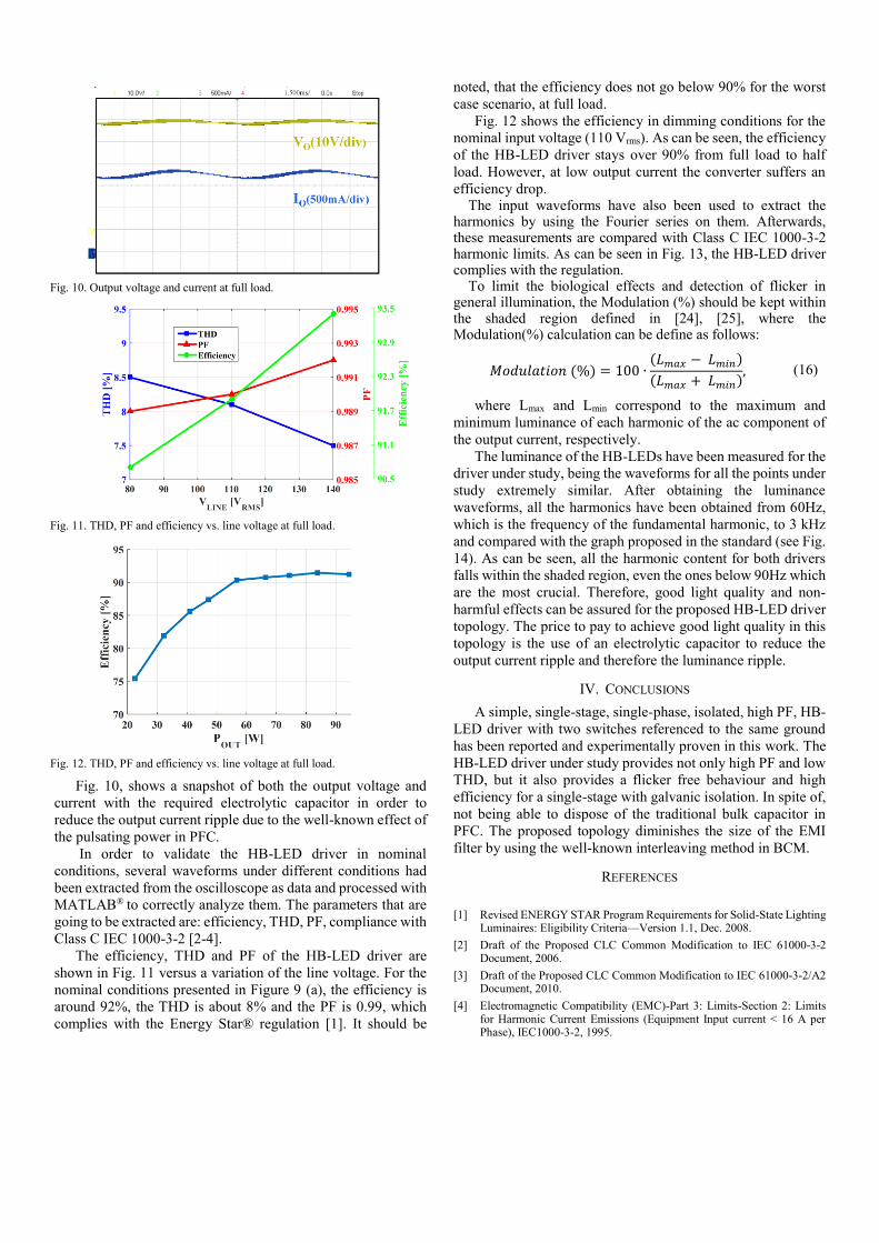
Fig. 10, shows a snapshot of both the output voltage and
current with the required electrolytic capacitor in order to
reduce the output current ripple due to the well-known effect of
the pulsating power in PFC.
In order to validate the HB-LED driver in nominal
conditions, several waveforms under different conditions had
been extracted from the oscilloscope as data and processed with
MATLAB® to correctly analyze them. The parameters that are
going to be extracted are: efficiency, THD, PF, compliance with
Class C IEC 1000-3-2 [2-4].
The efficiency, THD and PF of the HB-LED driver are
shown in Fig. 11 versus a variation of the line voltage. For the
nominal conditions presented in Figure 9 (a), the efficiency is
around 92%, the THD is about 8% and the PF is 0.99, which
complies with the Energy Star® regulation [1]. It should be
noted, that the efficiency does not go below 90% for the worst
case scenario, at full load.
Fig. 12 shows the efficiency in dimming conditions for the
nominal input voltage (110 Vrms). As can be seen, the efficiency
of the HB-LED driver stays over 90% from full load to half
load. However, at low output current the converter suffers an
efficiency drop. The input waveforms have also been used to extract the
harmonics by using the Fourier series on them. Afterwards, these measurements are compared with Class C IEC 1000-3-2 harmonic limits. As can be seen in Fig. 13, the HB-LED driver complies with the regulation.
To limit the biological effects and detection of flicker in general illumination, the Modulation (%) should be kept within the shaded region defined in [24], [25], where the Modulation(%) calculation can be define as follows:
𝑀𝑜𝑑𝑢𝑙𝑎𝑡𝑖𝑜𝑛 (%) = 100 ∙(𝐿𝑚𝑎𝑥 − 𝐿𝑚𝑖𝑛)
(𝐿𝑚𝑎𝑥 + 𝐿𝑚𝑖𝑛), (16)
where Lmax and Lmin correspond to the maximum and
minimum luminance of each harmonic of the ac component of
the output current, respectively.
The luminance of the HB-LEDs have been measured for the
driver under study, being the waveforms for all the points under
study extremely similar. After obtaining the luminance
waveforms, all the harmonics have been obtained from 60Hz,
which is the frequency of the fundamental harmonic, to 3 kHz
and compared with the graph proposed in the standard (see Fig.
14). As can be seen, all the harmonic content for both drivers
falls within the shaded region, even the ones below 90Hz which
are the most crucial. Therefore, good light quality and non-
harmful effects can be assured for the proposed HB-LED driver
topology. The price to pay to achieve good light quality in this
topology is the use of an electrolytic capacitor to reduce the
output current ripple and therefore the luminance ripple.
IV. CONCLUSIONS
A simple, single-stage, single-phase, isolated, high PF, HB-
LED driver with two switches referenced to the same ground
has been reported and experimentally proven in this work. The
HB-LED driver under study provides not only high PF and low
THD, but it also provides a flicker free behaviour and high
efficiency for a single-stage with galvanic isolation. In spite of,
not being able to dispose of the traditional bulk capacitor in
PFC. The proposed topology diminishes the size of the EMI
filter by using the well-known interleaving method in BCM.
REFERENCES
[1] Revised ENERGY STAR Program Requirements for Solid-State Lighting
Luminaires: Eligibility Criteria—Version 1.1, Dec. 2008.
[2] Draft of the Proposed CLC Common Modification to IEC 61000-3-2 Document, 2006.
[3] Draft of the Proposed CLC Common Modification to IEC 61000-3-2/A2 Document, 2010.
[4] Electromagnetic Compatibility (EMC)-Part 3: Limits-Section 2: Limits for Harmonic Current Emissions (Equipment Input current < 16 A per Phase), IEC1000-3-2, 1995.
Fig. 10. Output voltage and current at full load.
Fig. 11. THD, PF and efficiency vs. line voltage at full load.
Fig. 12. THD, PF and efficiency vs. line voltage at full load.
[5] Xiaogao Xie; Zhou Lan; Chen Zhao, "A new primary side controlled high power factor single-stage flyback LED driver," in Energy Conversion Congress and Exposition (ECCE), 2012 IEEE , vol., no., pp.3575-3580, 15-20 Sept. 2012.
[6] Peng Fang; Yan Fei Liu, "Single stage primary side controlled offline flyback LED driver with ripple cancellation," in Applied Power Electronics Conference and Exposition (APEC), 2014 Twenty-Ninth Annual IEEE , vol., no., pp.3323-3328, 16-20 March 2014.
[7] Liang Jia; Yan-Fei Liu; Fang, D., "High power factor single stage flyback converter for dimmable LED driver," in Energy Conversion Congress and Exposition (ECCE), 2015 IEEE , vol., no., pp.3231-3238, 20-24 Sept. 2015.
[8] Hongbo Ma; Cong Zheng; Wensong Yu; Jih-Sheng Lai, "Bridgeless electrolytic capacitor-less valley fill AC/DC converter for twin-bus type LED lighting applications," in Future Energy Electronics Conference (IFEEC), 2013 1st International , vol., no., pp.304-310, 3-6 Nov. 2013.
[9] Yiwen Zhang; Ke Jin, "A single-stage electrolytic capacitor-less AC/DC LED driver," in Electronics and Application Conference and Exposition (PEAC), 2014 International , vol., no., pp.881-886, 5-8 Nov. 2014.
[10] Shu Wang; Xinbo Ruan; Kai Yao; Zhihong Ye, "A flicker-free electrolytic capacitor-less ac-dc LED driver," in Energy Conversion Congress and Exposition (ECCE), 2011 IEEE , vol., no., pp.2318-2325, 17-22 Sept. 2011.
[11] Yang Yang; Xinbo Ruan; Li Zhang; Jiexiu He; Zhihong Ye, "Feed-Forward Scheme for an Electrolytic Capacitor-Less AC/DC LED Driver to Reduce Output Current Ripple," in Power Electronics, IEEE Transactions on , vol.29, no.10, pp.5508-5517, Oct. 2014.
[12] Linlin Gu; Xinbo Ruan; Ming Xu; Kai Yao, "Means of Eliminating Electrolytic Capacitor in AC/DC Power Supplies for LED Lightings," in Power Electronics, IEEE Transactions on , vol.24, no.5, pp.1399-1408, May 2009.
[13] Lamar, D.G.; Sebastian, J.; Arias, M.; Fernandez, A., "On the Limit of the Output Capacitor Reduction in Power-Factor Correctors by Distorting the Line Input Current," in Power Electronics, IEEE Transactions on , vol.27, no.3, pp.1168-1176, March 2012.
[14] L. H. Dixon, “High power factor preregulators for off-line power supplies”, Unitrode Power Supply Design Seminar, 1988, pp. 6.1-6.16.
[15] Kocher, M.J.; Steigerwald, R.L., "An AC to DC converter with high quality input waveforms," in Power Electronics Specialists conference, 1982 IEEE , vol., no., pp.63-75, 14-17 June 1982
[16] Thottuvelil, V.J.; Wilson, T.G.; Owen, H.A., "Analysis and design of a push-pull current-fed converter," in Power Electronics Specialists Conference, 1981 IEEE , vol., no., pp.192-203, June 29 1981-July 3 1981.
[17] Yang, E.X.; Yimin Jiang; Hua, G.; Lee, F.C., "Isolated boost circuit for power factor correction," in Applied Power Electronics Conference and Exposition, 1993. APEC '93. Conference Proceedings 1993., Eighth Annual , vol., no., pp.196-203, 7-11 Mar 1993.
[18] Huber, L.; Irving, B.T.; Jovanovic, M.M., "Review and Stability Analysis of PLL-Based Interleaving Control of DCM/CCM Boundary Boost PFC Converters," in Power Electronics, IEEE Transactions on , vol.24, no.8, pp.1992-1999, Aug. 2009.
[19] Nha Quang Trong; Huang-Jen Chiu; Yu-Kang Lo; Chin-Yu Lin; Alam, M.M., "Modified current-fed full-bridge isolated power factor correction converter with low-voltage stress," in Power Electronics, IET , vol.7, no.4, pp.861-867, April 2014.
[20] Jun Wen; Taotao Jin; Smedley, K., "A new interleaved isolated boost converter for high power applications," in Applied Power Electronics Conference and Exposition, 2006. APEC '06. Twenty-First Annual IEEE , vol., no., pp.6 pp.-, 19-23 March 2006.
[21] Wolfs, P.J., "A current-sourced DC-DC converter derived via the duality principle from the half-bridge converter," in Industrial Electronics, IEEE Transactions on , vol.40, no.1, pp.139-144, Feb 1993.
[22] de Aragao Filho, W.C.P.; Barbi, I., "A comparison between two current-fed push-pull DC-DC converters-analysis, design and experimentation," in Telecommunications Energy Conference, 1996. INTELEC '96., 18th International , vol., no., pp.313-320, 6-10 Oct 1996.
[23] S. Singer, "The application of `loss-free resistors' in power processing circuits," Power Electronics Specialists Conference, 1989. PESC '89 Record., 20th Annual IEEE, Milwaukee, WI, 1989, pp. 843-846 vol.2.
[24] IEEE Recommended Practices for Modulating Current in High-Brightness LEDs for Mitigating Health Risks to Viewers," in IEEE Std 1789-2015 , vol., no., pp.1-80, June 5 2015.
[25] “RP-16-10, Nomenclature and Definitions for Illuminating Engineering”, Illuminating Engineering Society.
[26] Z. Wang, S. Wang, P. Kong and F. C. Lee, "DM EMI Noise Prediction for Constant On-Time, Critical Mode Power Factor Correction Converters," in IEEE Transactions on Power Electronics, vol. 27, no. 7, pp. 3150-3157, July 2012.
[27] J. M. Kwon, E. H. Kim, B. H. Kwon and K. H. Nam, "High-Efficiency Fuel Cell Power Conditioning System With Input Current Ripple Reduction," in IEEE Transactions on Industrial Electronics, vol. 56, no. 3, pp. 826-834, March 2009.
[28] Z. Ouyang and M. A. E. Andersen, "Overview of Planar Magnetic Technology—Fundamental Properties," in IEEE Transactions on Power Electronics, vol. 29, no. 9, pp. 4888-4900, Sept. 2014.
[29] M. A. Saket, N. Shafiei, M. Ordonez, M. Craciun and C. Botting, "Low parasitics planar transformer for LLC resonant battery chargers," 2016 IEEE Applied Power Electronics Conference and Exposition (APEC), Long Beach, CA, 2016, pp. 854-858.
[30] L. Huber, B. T. Irving and M. M. Jovanovic, "Open-Loop Control Methods for Interleaved DCM/CCM Boundary Boost PFC Converters," in IEEE Transactions on Power Electronics, vol. 23, no. 4, pp. 1649-1657, July 2008.
[31] H. Y. Kanaan, A. Marquis and K. Al-Haddad, "Small-signal modeling and linear control of a dual boost power factor correction circuit," Power Electronics Specialists Conference, 2004. PESC 04. 2004 IEEE 35th Annual, 2004, pp. 3127-3133.
Fig. 13. Harmonic content of the input current for the topology under study
and compliance with Class C.
Fig. 14. Recommended flicker operation at full load for both drivers, P1789
[24].