ska paf beamformer - atnf
TRANSCRIPT
SKA PAF Beamformer SKA PAF beamformer Version 1.0 2011/01/03 Project: SKA Prepared by: John Bunton Approved by: Not Approved Keywords: SKA, Antenna, Phases Array Feed, Beamformer
Image Cover: Artist's impression of ASKAP at the Murchison Radio-astronomy Observatory (MRO). Credit: Swinburne Astronomy Productions. Design data provided by CSIRO.
Enquiries should be addressed to:
Document history
DATE AUTHOR SECTIONS/PAGES AFFECTED REVISION REMARKS 7 September 2010 John Bunton 0.1 First draft
Copyright and Disclaimer © 2010 CSIRO To the extent permitted by law, all rights are reserved and no part of this publication covered by copyright may be reproduced or copied in any form or by any means except with the written permission of CSIRO.
Important Disclaimer CSIRO advises that the information contained in this publication comprises general statements based on scientific research. The reader is advised and needs to be aware that such information may be incomplete or unable to be used in any specific situation. No reliance or actions must therefore be made on that information without seeking prior expert professional, scientific and technical advice. To the extent permitted by law, CSIRO (including its employees and consultants) excludes all liability to any person for any consequences, including but not limited to all losses, damages, costs, expenses and any other compensation, arising directly or indirectly from using this publication (in part or in whole) and any information or material contained in it.
i
Contents
1. INTRODUCTION ................................................................................................................ 1
1.1 Summary................................................................................................................... 1
1.2 Scope........................................................................................................................ 1
1.3 Glossary.................................................................................................................... 1
2. Dishes with Phased Array Feeds..................................................................................... 2
3. Other Beamformer calculation......................................................................................... 4
4. Beamformer Topology...................................................................................................... 4
5. Topology Selection ........................................................................................................... 6
6. FPGA capabilities for SKA phase 1 ................................................................................. 6
7. Downconversion or Direct Sampling .............................................................................. 7
8. Location of ADC ................................................................................................................ 8
9. Module partioning............................................................................................................. 8
10. SKA Phase 1 Cost Estimate ........................................................................................... 10
11. SKA Phase 2 .................................................................................................................... 11
12. ADC at the Focus ............................................................................................................ 12
13. Conclusion....................................................................................................................... 13
References ................................................................................................................................. 15
Appendix: Beamformer Specifications ................................................................................... 16
ii
List of Figures
Figure 1 Example of focal plane illuminations (credit S Hay) 2
Figure 2 Topology of a cross connected beamformer 5
Figure 3 Topology of a ring connected beamformer. 5
Figure 4 Partitioining into ADC/Coarse Filterbank and a separate beamformer 9
Figure 5 ADC at the antenna focus 13
List of Tables
Table 1 Some ptions for ADC placement 10
Table 2 Estimated cost of SKA Phase 1 beamformer, including data transport from the PAF, production start late 2018 11
Table 3 Estimated cost of SKA Phase 2 beamformer, including data transport from the PAF, production start late 2024 12
Table 4 Estimated cost of SKA Phase 2 beamformer, with ADC at the focus production start late 2024 13
INTRODUCTION
SKA PAF Beamformer• 2011/01/03, Version 1.0 1
1. INTRODUCTION
1.1 Summary
The possible methods of implementing a beamformer for a phased array feed at the focus of a parabolic dish are considered. The various beamforming algorithms and topologies are considered. One of these combinations is selected as the best fit to the requirements of the SKA which has a wide bandwidth and generates many beams.
Implementations of this design for SKA Phase 1 and 2 are described. The basic specifications for the design are derived from the ASKAP specifications [Appendix] with the bandwidth increased to 600MHz. Cost estimates for these implementations are given. These estimates are solely the author’s estimates and more work is needed to refine the values.
1.2 Scope
The design is developed from the ADC to the generation of beams. Not included are the implementation of the analogue system ahead of the ADC and the transport of the beam data to the correlator.
1.3 Glossary
Acronym Definition
ACM Array Covariance Matrix
SERDES Serial/deserialise. Self clocked high speed data transport
FFT Fast Fourier Transform
RF Radio Frequency
IF Intermediate Frequency
FPGA Field programmable gate array
ASIC Application specific integrated circuit
GPU Graphic processor unit
CPU Central Processing Unit
FX A type of correlator where the frequency transform (F) occurs before the multiplication (X) and accumulation
ASKAP Australian SKA Pathfinder
LOFAR Low Frequency Array
AIP Advance Instrumentation Program
2 SKA PAF Beamformer • 2011/01/03, Version 1.0
2. DISHES WITH PHASED ARRAY FEEDS
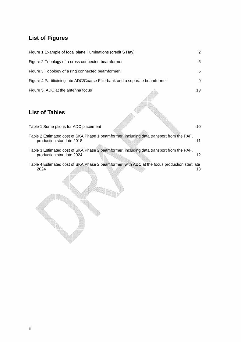
The operation of a phased array feed (PAF) at the focus of a dish is best understood in reception. For a point source illuminating a parabolic dish the illumination on the focal plane is not uniform. An example of the illumination is shown in Figure 1. The size of this illumination is proportional to wavelength. Each element of the phased array receives part of the incident energy. A beam is formed as a weighted sum of the signals from the feeds. The objective of the phased array feed beamformer is to maximise the collection of energy incident on the focal plane and minimise noise and possibly sidelobe levels. Various methods are available for calculating the weights needed to achieve this. One of the simplest being a conjugate match where the magnitude of the beamformer weights are proportional to the received electric field and the phase negated. The design of the algorithm to determine the weights is to be developed by the groups analysing the electromagnetics of the PAF.
−13
−19
0−18−18
−22
−26
−30
−30
−30
−13
−19
−22
−24
y (m)
x (m
)
−0.5 0 0.5
−0.5
−0.4
−0.3
−0.2
−0.1
0
0.1
0.2
0.3
0.4
0.5
Figure 1 Example of focal plane illuminations (credit S Hay)
For a bore sight source the phase is approximately uniform and as frequency changes only the amplitude changes with frequency. Consider a point located at the half power contour in Figure 1. As frequency increases, the amplitude at this point decreases because size of the focal spot decreases with frequency. At a high enough frequency the amplitude goes to zero and then becomes negative. For points further from the centre of the FPA variations are more rapid with frequency. In general the weighting needed to form a beam for the jth port of the phased array feed has a transfer function Hj(ω).
For sources off bore sight there is also a phase gradient across the focal plane. As well as this there is aberration which makes the energy distribution in the focal plane asymmetric. Other factors that complicate Hj(ω) and the optimal weight needed to form a beam are the frequency response of the receiver chain and LNA, and coupling between elements of the array. Of these, the multiple RF and IF filters in the receiver chain can introduce the fastest changing perturbations. Correcting for these implies an IRR filter of order 7 or more. But in general Hj(ω) is not minimum phase and is best implemented as an FIR filter in the digital domain. The order of the filter is ~40 or more.
DISHES WITH PHASED ARRAY FEEDS
SKA PAF Beamformer• 2011/01/03, Version 1.0 3
The contribution Cj of PAF port j to a beam is
)()()( tvthtC jjj ∗=
where * denotes convolution vj(t) is the voltage at the receiver output and hj(t) is the impulse response of the transfer function Hj(ω). The beam B(t) is the sum of all these contribution over all PAF ports:
∑ ∗=ports allover
)()()(j
jj tvthtB
It is assumed that the voltages are digitised at a rate of ~2.5 BW, where the values vj(t) are real, and BW is the bandwidth processed in the correlator. The factor of 2.5 is to allow for transition bands that are later discarded. Counting only the multiplication then the compute CLt load of this time domain beamformer is
CLt = 2.5 Nb Nf Np BW multiplies/s
Where Nb is the number of beams (single pol), Nf is the average number of taps in the
FIR filters, >40, and Np is the average number of ports used to form each beam.
An alternative definition is obtained by noting that if the input is processed by a filterbank then for sufficiently small frequency bands the filter for each band reduces to a single complex weight. The outputs of the filterbank vj.ω(t) for frequency channel ω are complex. The input to the filterbank is real data with sample rate 2.5 BW. An oversampling polyphase filterbank [1] of length L and oversampling ratio k (~1.2) is assumed. The short FIR filters at the input to the FFT in the filter bank are of length ~10 and the cost of the FFT is ~3(log4(L)-1) real multiplies per input sample. By using the real and imaginary inputs for different signals the cost of the FFT is reduced to ~1.5(log4(L)-1) multiplies per input sample. The compute load CLfb of the filterbank in multiplies per second is
CLfb = 2.5 k Np [10 + 1.5(log4(L)-1)]BW multiplies/s
~ 2.5 x 16 Np BW multiplies/s for a 1000 channel filterbank
The filterbank generates L/2 independent frequency channels. Of these L/2.5 are used to generate beams that are processed by the correlator. The sample rate for each frequency channel is (k 2.5BW/L). The compute load to the form the beams becomes
CLb = 4 Nb Np L/2.5 (k 2.5BW/L) (4 real multiplies per complex weight)
~ 5 Nb Np BW multiplies/s
The compute load CLf for a frequency domain beamformer is
CLf ~ (40+ 5 Nb) Np BW multiplies/s
The break even point between a frequency domain and time domain beamformer occurs when CLf is equal to CLt:
4 SKA PAF Beamformer • 2011/01/03, Version 1.0
40+ 5 Nb = 2.5 Nb Nf
2 + 16/ Nb = Nf
For the SKA Nb is of order 60 (30 dual polarisation beams) so the term of the left is ~2.3. The number of taps for a time domain beamformer FIR filter is greater than 40. Hence, the frequency domain approach is an order of magnitude more efficient in terms of the number of multiplication when compared to a time domain beamformer.
An additional factor in favour of a frequency domain beamformer is that the SKA will use an FX correlator [2] which requires a filterbank before the correlation operation. The frequency domain beamformer provides an initial stage of this filterbank operation. The beamformer filterbank decimates the data to a ~1MHz resolution. The final frequency resolution is obtained by cascading a second or third filterbank [3]. A second ‘fine’ filterbank of order ~10 to 1000 gives frequency resolutions from ~100 kHz to ~1 kHz. At the 1 kHz resolution, the number of frequency channels is about half a million. This exceeds SKA requirements and in practice only part of the full bandwidth would be processed at this frequency resolution. For higher frequency resolutions, a third filterbank stage is needed but as only part of the bandwidth is processed the cost of any third stage filterbank is low.
3. OTHER BEAMFORMER CALCULATION
As well as the processing needed for beamforming, the beamformer must calculate the data needed to calibrate the array and calculate the beam weights. The main input into the beam weight calculations is the Array Covariance Matrix (ACM). This array contains the autocorrelations and all the cross correlations between array elements. The correlations are calculated with a frequency resolution of ~1MHz for a PAF operating above 700MHz. The 1 MHz bandwidth corresponds to the bandwidth across which the beam weights are approximately constant. Calculation of the full ACM across the full bandwidth is expensive. On average each complex input value results in n/2 complex multiplication, where n is the number of PAF elements. This compares to at most 2m complex multiplications in the beamforming operation, where m is the number of dual polarisation beams. For a practical beamformer the number of complex multiplications is less possibly ~2m/3. As an example in the ASKAP [4] beamformer there are 94 complex multiplications per input sample for the full ACM and ~25 complex multiplications for the beamforming.
Assuming the ACM changes slowly with time then the ACM compute load can be reduced by decimating the calculation in time and frequency. In ASKAP only 1/5 of all frequency channels are processed at one time and for these only every fourth value is used. This reduces the ACM compute load by a factor of ~20.
4. BEAMFORMER TOPOLOGY
The size of an SKA PAF beamformer precludes it being instantiated in a single processing block (ASIC, FPGA, GPU or CPU). This requires data connections to redistribute the data either before or after beamforming.
BEAMFORMER TOPOLOGY
SKA PAF Beamformer• 2011/01/03, Version 1.0 5
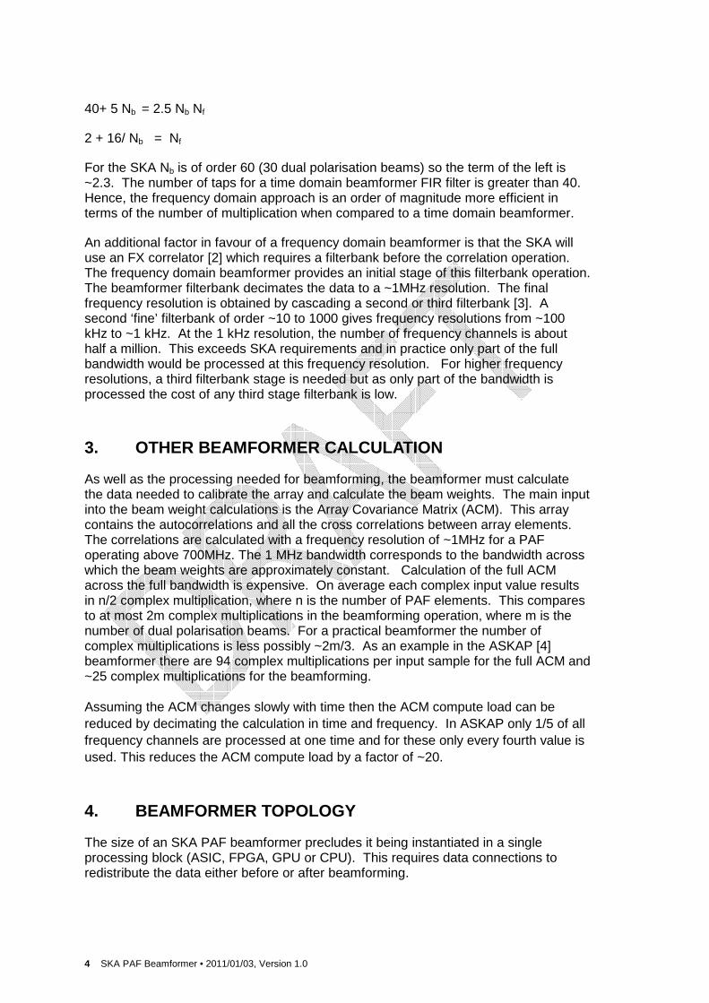
If the coarse filterbank is in a separate processing block to the beamforming then a cross connect as shown in figure 2 is possible. After the cross connect each beamformer block will have data for all ports but for a limited number of frequency channels. An example of this design is the ASKAP 304MHz beamformer [4] where each digitisers and coarse filterbank module processes four analogue inputs. The output from the coarse filterbank is packetized onto 16 2.5Gb/s lanes which are transported on 4 10Gb/s optical links. At the beamformer the 16 lanes are distributed across the 16 beamforming boards. Each board receives data for one lane which carries 19MHz of bandwidth.
Figure 2 Topology of a cross connected beamformer
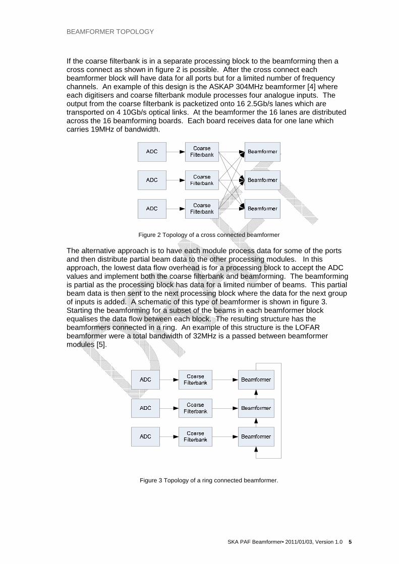
The alternative approach is to have each module process data for some of the ports and then distribute partial beam data to the other processing modules. In this approach, the lowest data flow overhead is for a processing block to accept the ADC values and implement both the coarse filterbank and beamforming. The beamforming is partial as the processing block has data for a limited number of beams. This partial beam data is then sent to the next processing block where the data for the next group of inputs is added. A schematic of this type of beamformer is shown in figure 3. Starting the beamforming for a subset of the beams in each beamformer block equalises the data flow between each block. The resulting structure has the beamformers connected in a ring. An example of this structure is the LOFAR beamformer were a total bandwidth of 32MHz is a passed between beamformer modules [5].
Figure 3 Topology of a ring connected beamformer.
6 SKA PAF Beamformer • 2011/01/03, Version 1.0
The proposed SKA Phase 1 beamformer [Appendix] has 188 ADC inputs and generates 72 beams (36 dual pol). This means that the partial beam data flow to an adjacent processing block is ~0.4 times the total coarse filterbank data. The total data flow overhead in the cross connected beamformer is the coarse filterbank data, as it is transported from the filterbanks to the beamformers. Thus for the SKA Phase 1 beamformer the cross connect beamformer has less data flow than a ring connected beamformer with three beamformer modules. Current beamformer designs for PAFs have ~50 processing blocks and a ring beamformer is not appropriate. But at the time of the SKA there will be fewer processing blocks.
5. TOPOLOGY SELECTION
A second requirement on the beamformer is that it calculate the Array Covariance Matrix (ACM). The ACM is needed for the calculation of beam weights. The ACM is found by measuring the cross correlation between all input signals, including autocorrelation. In the cross connected beamformer topology, each processing block has data for all PAF ports for some part of the bandwidth. Each beamformer processing block can calculate the ACM for its own frequency channels. In a ring connected beamformer only part of the PAF data are available in each processing block. To implement the ACM the equivalent of a full cross connect is needed in addition to the ring connection for beam data. Hence, the preferred topology for the SKA beamformer is that of the cross connected beamformer.
6. FPGA CAPABILITIES FOR SKA PHASE 1
After taking into account development, production and installation time the hardware installed for SKA Phase 1 in 2019 will be using technology that is released in 2017-2018. Mid-sized FPGA that will be available in 2011 will have ~2000 multipliers and cost less than $1000 in large quantities. FPGA generation are introduced every ~3 years and the number of multipliers roughly double each time. Hence, midsizes FPGAs available in 2017 are estimated to have 8,000 multipliers, again at a cost of less than $1000 per piece. Using such devices would see hardware development through 2018 with production and installation in the last year of Phase 1 construction: 2019.
The clock rate of FPGA will also increase over time, conservatively this will increase at least 10% per generation so compare to current devices which easily process data at 300MHz the 2017 devices should process data at 400MHz. The processing capability of each FPGA is expected to be 3.2T multiplies/s
SKA phase 1 with a bandwidth 600MHz requires ~30T multiplies/s [Appendix] and hence needs ~9 FPGAs to implement the beamformer processing. The cost of systems using these FPGA is about twice that of the FPGA used which gives an estimated cost for the boards performing the beamforming of less than $18,000.
DOWNCONVERSION OR DIRECT SAMPLING
SKA PAF Beamformer• 2011/01/03, Version 1.0 7
7. DOWNCONVERSION OR DIRECT SAMPLING
The cost of ADC and digital signal processing continues to decrease at a faster rate than the cost of analogue components. This has seen the gradual migration of the ADC in radios to points closer and closer to the input amplifier. This suggests that for the SKA the ADC will directly sample the RF signal. Here direct sampling refers to a system with no analogue mixer. Only amplification and filtering occurs before the ADC. The ADC could be operating at base band (0 to Fs/2) or any of the higher Nyquist zones such as (Fs/2 to Fs) where Fs is the sampling frequency. If antialiasing filters with fairly relaxed constraints are used then about 80% of the second Nyquist zone is available. This provides a 50% fractional bandwidth. For fractional bandwidth higher than 65% second order intermodulation product start to occur in band making analogue design harder. Here it is assumed that for the SKA phase 1 the fractional bandwidth is 50-60%.
The high fractional bandwidth means ADC sample rates are not reduced if there is a downconversion system. Hence, direct sampling of the PAF signal is preferred as it eliminates the cost of local oscillators, mixers and IF filters needed in a heterodyne system. The wide fractional bandwidth means direct sampling comes at no cost penalty in the ADC or digital hardware.
Direct sampling also has the useful property that the sample clock, even if it clocking at half the sample rate, produces frequency spurs at the band edges. This data is normally discarded, so there are no inband spurious signals from the ADC clock. This is not the case for a heterodyne system where it is hard to avoid inband spurious signals.
For a PAF going to 1.5GHz an ADC operating in the second Nyquist zone and sampling at ~1.65GS/s is sufficient with appropriate filters. The1.65GS/s sampling rate allows the band 0.9 to 1.5GHz to be covered. Reducing the sample rate to 1.1 GS/s covers the band 0.6 to 1GHz in the second Nyquist zone. These two bands cover a 2.5:1 frequency band which the PAF is expected to cover. To achieve a greater bandwidth a third frequency band could be introduced. A more expensive alternative is to capture the lower band in the first Nyquist zone of an ADC. For this the ADC sample rate needs to be about 2.2GS/s, 1.33 times higher. Frequency coverage down to DC is now possible. This last option has the advantage the bandwidth for both bands can be 600MHz, compared to 400MHz for the lower band when the sampling rate is 1.1GS/s. The extra digital signal processing in the filterbanks is small. The main cost is due to the higher performance ADC needed.
The computational cost of an oversampling filterbank is ~40BW multiplications/s for real input data. For the 600MHz bandwidth proposed this is 24x109 multiplies/s per input. In FPGAs expected in 2017 a mid sized part has 8000 multipliers that operate at ~400MHz or 3200x109muliplications/s. Thus a single FPGA could process up to ~150 ports. For 200 port at least two FPGAs are needed. It will not be the processing power that limits the design, rather it is expected that it will be the ADCs, analogue filters and the I/O into and out of an FPGA. But independent of the number of FPGA the FPGA cost for the filterbanks will be approximately that of two mid range FPGAs: ~$2000.
8 SKA PAF Beamformer • 2011/01/03, Version 1.0
8. LOCATION OF ADC
Transport of data from the PAF could be either analogue on coax, RF over fibre or digital on fibre. A digital over fibre solution requires the ADC to be at the focus. In [4] discrete digitisers are used and the size of the complete digitiser system is about half a cabinet. It is unlikely that a system using discrete ADC will be small and light enough to be installed at the focus of a dish by 2017. Work on multichannel ADCs with integrated laser drivers should be pursued for SKA phase 2.
For SKA phase 1 it is likely that the data from the PAF will be RF either on fibre or coax. In [4] data is transport on coaxial cables to the pedestal. The coaxial cable cost is ~$3m and with connectors the 40m of cable cost ~$150 per connection. At the time of the design decision, 2008, DBF lasers for RF over fibre cost ~$1000 this has now come down to under $150 making it cheaper than coaxial cable for RF data transport from the PAF to the pedestal. By 2017 the cost of RF over fibre system is expected to be ~$100 including the post detection amplifiers and filters. The DFB lasers are single mode and the location of the ADC can be up to 10km from the antenna.
Coax cable connection between the digitiser and the PAF is still an option as long as the connection is short. This means the ADC must be above the antenna mount and a possible location is under the antenna surface. This can reduce the cost the cable to ~$50 as well as greatly reducing the cable loss as the cable is not only shorter it can also be thicker.
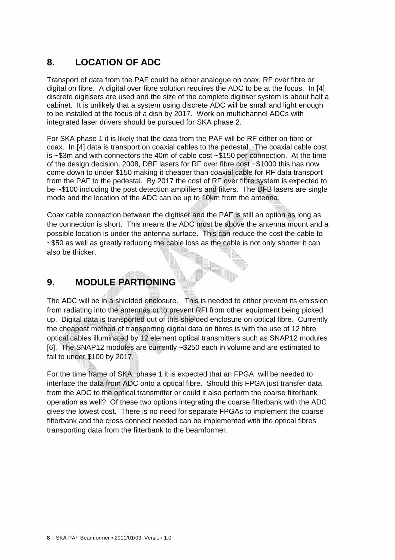
9. MODULE PARTIONING
The ADC will be in a shielded enclosure. This is needed to either prevent its emission from radiating into the antennas or to prevent RFI from other equipment being picked up. Digital data is transported out of this shielded enclosure on optical fibre. Currently the cheapest method of transporting digital data on fibres is with the use of 12 fibre optical cables illuminated by 12 element optical transmitters such as SNAP12 modules [6]. The SNAP12 modules are currently ~$250 each in volume and are estimated to fall to under $100 by 2017.
For the time frame of SKA phase 1 it is expected that an FPGA will be needed to interface the data from ADC onto a optical fibre. Should this FPGA just transfer data from the ADC to the optical transmitter or could it also perform the coarse filterbank operation as well? Of these two options integrating the coarse filterbank with the ADC gives the lowest cost. There is no need for separate FPGAs to implement the coarse filterbank and the cross connect needed can be implemented with the optical fibres transporting data from the filterbank to the beamformer.
MODULE PARTIONING
SKA PAF Beamformer• 2011/01/03, Version 1.0 9
ADCsCoarse
Filterbanks
ADCsCoarse
Filterbanks
ADCsCoarse
Filterbanks Beamformer
BeamformerADCs
Coarse
Filterbanks
ADCsCoarse
Filterbanks
Short Range
Optical
Connection
Figure 4 Partitioining into ADC/Coarse Filterbank and a separate beamformer
The current SNAP12 modules use multimode fibre which limits the range of the connection to tens of metres. It is unlikely that competitive single mode fibre technology will be available by 2017. The use of multimode fibres mean the ADC and the beamformer will be located in the same structure.
The two options for data transport to the ADCs are coaxial cable and RF over fibre. For coaxial cable a possible location of the digitisers is in a shielded enclosure on the feed boom for offset fed reflectors, underneath the dish surface or a vertex room if one exists. The beamformer is also located at the antenna, in the pedestal, vertex room, or the control enclosure which in some antenna designs is suspended from the azimuth axis and rotates with the antenna. In all cases only optical fibres are routed through the cable wraps.
With RF over fibre there are a greater range of options available as links are on single mode fibre. The total range of the transmission is at least 10km. The system could be located at the antenna, a control building associated with an antenna, or the central building housing the correlator. For antennas within the core the last option is appealing as the links from the beamformer to the correlator could also be on low cost multimode fibre links.
For antennas further than ~10km from the correlator building there is the option of combining the ~10km reach of RF over fibre with the ~10km reach of VSCEL-based low-cost digital transmission. In this case, the ADC/filterbank and beamformer are located in a separate building that is ~10km from the correlator. This allows the antenna to be located up to 20km from the correlator and still use low cost digital data transmission to the correlator.
10 SKA PAF Beamformer • 2011/01/03, Version 1.0
Table 1 Some options for ADC placement
ADC Input ADC/Filterbank Beamformer Beamformer output
Antenna – correlator distance
Coaxial Above any axis of rotation
Pedestal, vertex, or control system enclosure
Single mode fibre
10km low cost 100km high cost Any multi hop
RF over Fibre
Correlator building
Correlator building Multi mode fibre
Up 10km
RF over Fibre
Pedestal Pedestal Single mode fibre
10km low cost 100km high cost Any multi hop
RF over Fibre
Separate building
Separate building Single mode fibre
20 km low cost 110km high cost Any multi hop
10. SKA PHASE 1 COST ESTIMATE
The basic hardware for all options presented in table 1 is the same. The items making up this hardware are: ADC, Filtebank FPGA system, 12-fibre optical links, and beamformer FPGA system. Previously it is estimated that the beamformer, excluding fibre optic systems would cost ~$18,000 and have 9 processing FPGAs. To simplify the design cycle this can be implemented on two processing boards with 4 or 5 FPGAs each. Digital data to be transported to the beamform comes from ~200 PAF ports, each with 600MHz of bandwidth. Assuming 8 bit samples and oversampling of the data by 1.185 then the total data rate is 11.4Gb/s per port and 2.28Tb/s total. A SNAP 12 with 10Gb/s per port transports 120Gb/s so ~19 are needed. If there are two beamformer boards then 20 12-fibre links are needed with 10 connecting to each beamformer. The ADC can be implemented as 10 subsystems each processing 20 analogue inputs. Each ADC subsystem has, for example, 5 quad-channel ADCs and a single ~2000 multiplier FPGAs. For these the ten FPGA cost is expected to be the same as two and a half midsized 8000 multiplier FPGAs: $2500.
ADCs that are close to the performance needed for a 1.65GS/s system are currently ~$70 per channel and possibly lower at the volumes needed for the SKA. Extrapolating to 2017 it might be expected that they cost $40 per channel, giving an estimated ADC cost of $8,000. The boards holding the FPGAs and ADC are ~$1000 including all other parts and assembly. For the 10 ADC boards this is ~$10,000. And the SNAP12 connections are ~$600 in small quantities for the transmitter, receiver and cable. Estimate large volume price probably close to $200 in 2017 or $4000 for the full systems.
For RF over Fibre analogue data transmission it is estimated each channel will cost ~$100. Coaxial cable connection will be similar, depending on the length of the cable. This gives a cost of around $20,000 to get the RF data from the PAF to the ADC. Finally, the hardware needs to be housed in a card cage, a rack and have power
SKA PHASE 2
SKA PAF Beamformer• 2011/01/03, Version 1.0 11
supplies. Assuming these cost about $10,000 then the total cost is estimated to be $73,000. The cost data is summarised in the table below.
Table 2 Estimated cost of SKA Phase 1 beamformer, including data transport from the PAF, production start late 2018
Beamformer component Cost Beamformer boards and FPGAs $18,000 ADC-Beamformer optical links $4,000 Coarse filterbank FPGA $2,500 ADC $8,000
ADC / Coarse filterbank boards $10,000 Transport of Analogue data to ADC $20,000 Card cages, racks, power supplies $10,000 Total $72,500 The above cost does not include the data transport from the beamformer to the correlator which could be up to 1Tb/s. It is expected that 100Gb/s links will be becoming commodity items and cost at most a couple of hundred dollars each. So for spans of up to 10km the added cost would be small.
11. SKA PHASE 2
By the time of Phase 2 construction there will have been at least two more generations of FPGAs. This will reduce the beamformer to a single board which could be implemented with a total FPGA cost of about $2,500. It should be possible to build the board house it and provide power for about double this: $5,000. The main problem is getting the data to the ADC and then to the beamformer. For RF over Fibre and coaxial cable the standard approaches use of a single connector for each signal transported. For RF over fibre this is required because single mode fibre is mandatory for connections that traverse a cable wrap. The Phase 1 design also used lumped element filters. The need for individual connectors and lumped element filters makes it hard to reduce the cost of transporting data to the ADC. The ADC themselves will probably halve in cost to ~$4,000 for off the shelf components. The cost of optical digital data transport to the beamform will also decrease and will probably be less than $2,000. Hence all FPGAs, the beamformer and data transport to the beamformer could drop to $12,000. But this cost could be dwarfed by the cost of ADC boards and the transport of data to the boards, up to $30,000.
One possibility for reducing cost is the development of multifibre single mode optical transmitters. This may come with 100Gb Ethernet. The second part of the analogue path is the amplifiers, filters, switches, attenuators etc. Development of an integrated solution for these should be part of and Advanced Instrumentation Program (AIP). If RF over Fibre data transport could be brought down to $50 per channel, the analogue filters/amplifiers etc to $10 per channel then getting the analogue data to the ADC could cost $12,000. With say 4 fibres in each link and 16 links to a single ADC board then a single board might process 64 signals. There would be 3 ADC boards in each beamformer, bringing the board cost for the ADC to ~$3000. The three ADC and single beamformer boards might be housed in pizza boxes and the cost of power
12 SKA PAF Beamformer • 2011/01/03, Version 1.0
supplies etc could be ~$4,000. The breakdown of estimated cost for the full beamformer is shown in Table 3.
Table 3 Estimated cost of SKA Phase 2 beamformer, including data transport from the PAF, production start late 2024
Beamformer component Cost Beamformer board and FPGAs $5,000 ADC-Beamformer digital optical $2,000 Coarse filterbank FPGA $1,000 ADC $4,000
ADC / Coarse filterbank boards $3,000 Transport of Analogue data to ADC $12,000 Card cages, racks, power supplies $4,000 Total $31,000
With this estimate the transport of the analogue data to the ADC is by far the major component, so part of an Advanced Instrument Program might look into ways of reducing this cost. However, such RF over Fibre Links are critically dependent on the actual manufactures and it may be hard to find a suitable collaborator. To reduce cost it is suggested that the ADC should be at the focus.
12. ADC AT THE FOCUS
With the ADC at the focus one of the more important issues to be faced is digital noise leaking into the LNA and feed system. Measures will be taken to shield the ADC from the rest of the system but it is also important to reduce the RFI generated by the ADC. With the preceding designs one of the major sources of RFI was the transmission of the digital data to the FPGA that then drives the optical link to the beamformer. The best option is an integrated ADC and optical laser driver. This could be the basis of an Advanced Instrumentation Program (AIP). Already ADCs such as the time based ADC [7] have outputs suitable for direct transmission over optical links.
The target for such and ADC would be a 1.65GS/s device with 12 analogue inputs and direct drive of a 12 fibre optical ribbon. For an 8 bit converter running at 1.65Gb/s the data rate is ~15Gb/s per link when overheads are included. Already FPGA are achieving over 11Gb/s with 28Gb/s promised in the next generation devices. For low cost, VSCEL based lasers driving multimode fibre would be the choice. Current SNAP 12 devices have been reported at 8.5Gb/s and the 15Gb/s should achieved in 10 years time or less. About 16 of these ADC/Laser combinations are need for a PAF. Each could be in an individual RFI enclosure with 12 RF inputs, an ADC clock input, DC power, a 12 fibre output ribbon and some low speed optical connection for control and monitoring. This enclosure is quite small and possibly cost ~$200 each, including connectors.
Assuming the 12 input ADC, developed within an AIP, is ~$100 per unit then the cost of ADCc is ~$1600. The cost of the laser drives should also fall. Here it is estimated that a link will cost $200 including the lasers, cable and optical RX. No coarse filterbank is implemented with the ADC. In the Phase 1 system ~12 FPGA need for the beamformer and coarse filterbank. In Phase 2 this is now reduced to 3-4 FPGAs
CONCLUSION
SKA PAF Beamformer• 2011/01/03, Version 1.0 13
so the full digital processing system is reduced to a single board. It will have as input 16 twelve fibre ribbons. This board does the beamforming and the coarse filterbank operations. Cost of the board excluding optics is estimated to be twice the FPGA cost: ~$8000. A “pizza box” enclosure for the boards and power supplies and cooling adds possibly $2000.
The board generates ~36 dual pol beams at 600MHz bandwidth. The output data is at ~16bit/HZ for a total output data rate of ~700Gb/s. Including overheads this can be transported on 8 100GE links which will be commodity items in 2024. These should cost no more than $200 each. The cost of all the items listed above are tabulated in Table 4
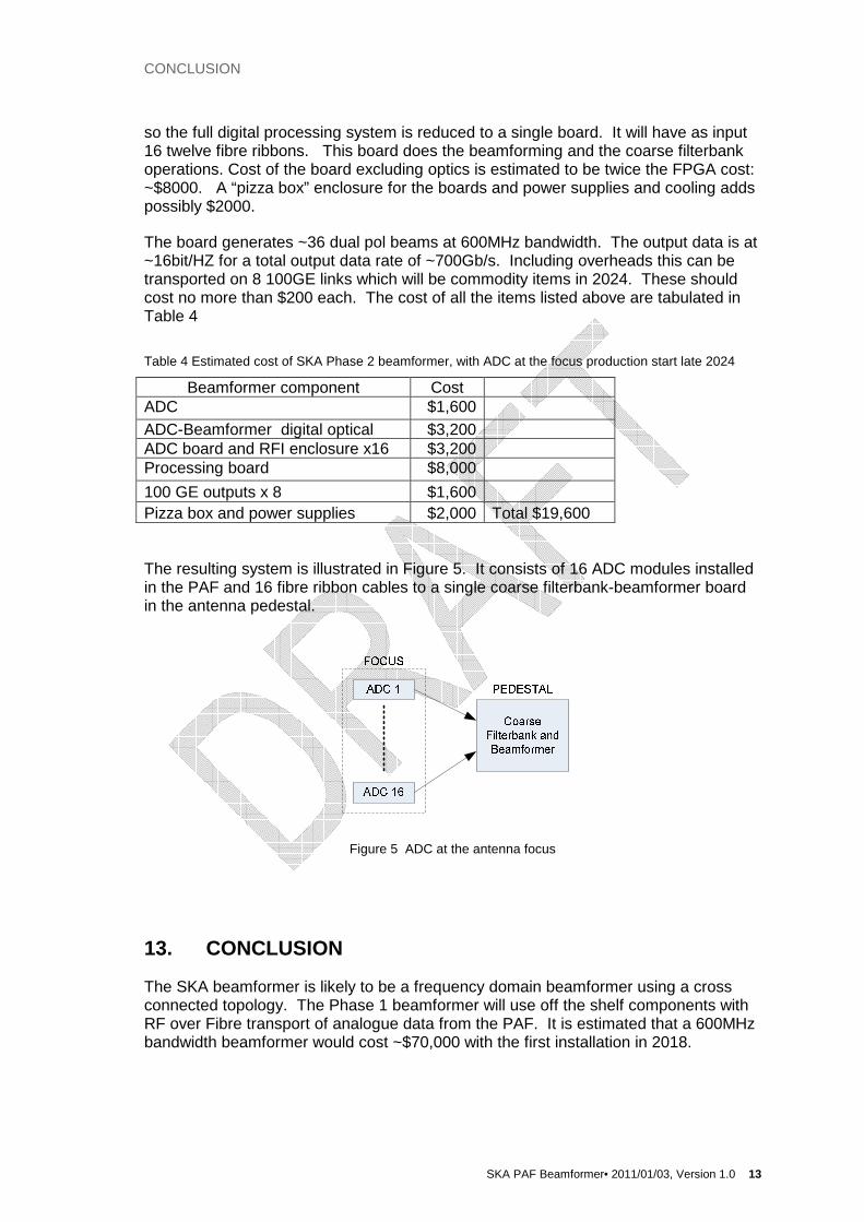
Table 4 Estimated cost of SKA Phase 2 beamformer, with ADC at the focus production start late 2024
Beamformer component Cost ADC $1,600 ADC-Beamformer digital optical $3,200 ADC board and RFI enclosure x16 $3,200 Processing board $8,000
100 GE outputs x 8 $1,600 Pizza box and power supplies $2,000 Total $19,600
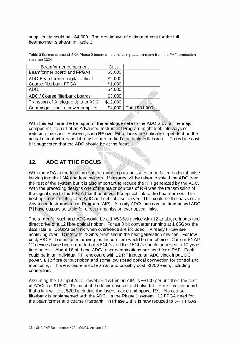
The resulting system is illustrated in Figure 5. It consists of 16 ADC modules installed in the PAF and 16 fibre ribbon cables to a single coarse filterbank-beamformer board in the antenna pedestal.
Figure 5 ADC at the antenna focus
13. CONCLUSION
The SKA beamformer is likely to be a frequency domain beamformer using a cross connected topology. The Phase 1 beamformer will use off the shelf components with RF over Fibre transport of analogue data from the PAF. It is estimated that a 600MHz bandwidth beamformer would cost ~$70,000 with the first installation in 2018.

14 SKA PAF Beamformer • 2011/01/03, Version 1.0
For SKA Phase 2 time exists to implement Advanced Instrumentation Programs. With this program a multichannel ADC with integrated optical laser driver could be developed that would allow the ADC to be located at the focus. This might provide a beamformer and ADC system for ~$20,000. A less ambitious system would continue to use RF over Fibre to transport data from the PAF. In this case the estimated cost is ~$30,000.
REFERENCES
SKA PAF Beamformer• 2011/01/03, Version 1.0 15
REFERENCES
[1] Harris, f.j., ‘Multirate Signal Processing fro Communication Systems’, 2004, Prentice Hall PTR, Upper Saddle River, New Jersey
[2] Bunton, J.D. ‘Multi-resolution FX Correlator’, ALMA memo 447, Feb 2003, http://science.nrao.edu/alma/aboutALMA/Technology/ALMA_Memo_Series/main_alma_memo_series.shtml
[3] Bunton, J.D., ‘SKA Correlator Advances’, Experimental Astronomy, Volume 17, 1-3, pp 251-259, June 2004
[4] D eBoer, D.R., et al, “ Australian SKA Pathfinder: A High-Dynamic Range Wide-Field of View Survey Telescope Array” IEEE Proceedings, Vol 97, Number 8, pp1507-1521 Aug 2009
[5] Gunst, A.W., Kant. G.W. “Signal Transport And Processing At The Lofar Remote Stations” Proceedings of the XXVIIIth URSI General Assembly, New Delhli, India, October 23-29, 2005, paper J06.4(0464)
[6] http://www.reflexphotonics.com/products_2.html
[7] Townsend, K.A.; Macpherson, A.R.; Haslett, J.W.; , "A fine-resolution Time-to-Digital Converter for a 5GS/S ADC," , Proceedings of 2010 IEEE International Symposium on Circuits and Systems (ISCAS), pp.3024-3027, 30 May 2010 - 2 June 2010 Available: http://ieeexplore.ieee.org/stamp/stamp.jsp?tp=&arnumber=5538004&isnumber=5536941
[8] Bunton, J.D., Hay, S.G., ‘Achievable Field of View of Chequerboard Phased Array Feed’, International Conference on Electromagnetics in Advanced Applications (ICEAA’10), September 20-24, 2010, Sydney Australia
APPENDIX: BEAMFORMER SPECIFICATIONS
16 SKA PAF Beamformer • 2011/01/03, Version 1.0
APPENDIX: BEAMFORMER SPECIFICATIONS
PAF beamforming is a new concept in radio astronomy and no full specification beamformer is operational yet. The system that is closest to being fielded operationally is the ASKAP beamformer [4]. This is expected to occur in the first half of 2011. Estimates of the achievable field of view of this beamformer have be made [8]. The beamformer generates 36 beams and at 1.45GHz they are separated by λ/D radians on the sky. The resulting beam pattern, for the sum of all beams, is quite complex. To quantify the field of view a definition was proposed where the field of view is the integral of the sensitivity squared divided by the square of the maximum sensitivity. For a single beam this definition differs from the traditional half power beam area by a factor of ~.75.
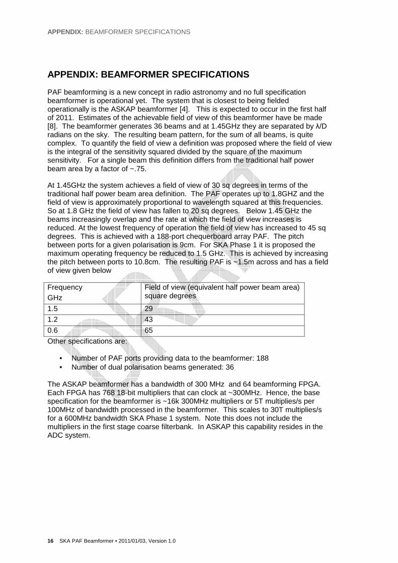
At 1.45GHz the system achieves a field of view of 30 sq degrees in terms of the traditional half power beam area definition. The PAF operates up to 1.8GHZ and the field of view is approximately proportional to wavelength squared at this frequencies. So at 1.8 GHz the field of view has fallen to 20 sq degrees. Below 1.45 GHz the beams increasingly overlap and the rate at which the field of view increases is reduced. At the lowest frequency of operation the field of view has increased to 45 sq degrees. This is achieved with a 188-port chequerboard array PAF. The pitch between ports for a given polarisation is 9cm. For SKA Phase 1 it is proposed the maximum operating frequency be reduced to 1.5 GHz. This is achieved by increasing the pitch between ports to 10.8cm. The resulting PAF is ~1.5m across and has a field of view given below
Frequency GHz
Field of view (equivalent half power beam area) square degrees
1.5 29
1.2 43
0.6 65
Other specifications are:
• Number of PAF ports providing data to the beamformer: 188 • Number of dual polarisation beams generated: 36
The ASKAP beamformer has a bandwidth of 300 MHz and 64 beamforming FPGA. Each FPGA has 768 18-bit multipliers that can clock at ~300MHz. Hence, the base specification for the beamformer is ~16k 300MHz multipliers or 5T multiplies/s per 100MHz of bandwidth processed in the beamformer. This scales to 30T multiplies/s for a 600MHz bandwidth SKA Phase 1 system. Note this does not include the multipliers in the first stage coarse filterbank. In ASKAP this capability resides in the ADC system.