skp engineering collegeece.skpec.edu.in/.../11/rf-and-microwave-engineering.pdf · 2018-04-05 ·...
TRANSCRIPT

S.K.P. Engineering College, Tiruvannamalai VIISEM
Electronics And Communication Engineering Department 1 RF and Microwave Engineering
SKP Engineering College
Tiruvannamalai – 606611
A Course Material
on
RF And Microwave Engineering
By
A.Parimala Assistant Professor
Electronics and Communication Engineering Department
S.K.P. Engineering College, Tiruvannamalai VIISEM
Electronics And Communication Engineering Department 2 RF and Microwave Engineering
Quality Certificate
This is to Certify that the Electronic Study Material Subject Code: EC6701
Subject Name: RF and Microwave Engineering
Year/Sem: IV/VII
Being prepared by me and it meets the knowledge requirement of the University curriculum.
Signature of the Author
Name: A.Parimala
Designation: Assistant Professor
This is to certify that the course material being prepared by Ms.A.Parimala is of the adequate quality. She has referred more than five books and one among them is from abroad author. Signature of HD Signature of the Principal
Name: Name: Dr.V.Subramania Bharathi
Seal: Seal:

S.K.P. Engineering College, Tiruvannamalai VIISEM
Electronics And Communication Engineering Department 3 RF and Microwave Engineering
EC6701 RF AND MICROWAVE ENGINEERING L T P C 3 1 0 4 OBJECTIVES:
• To inculcate understanding of the basics required for circuit representation of RF networks.
• To deal with the issues in the design of microwave amplifier. • To instill knowledge on the properties of various microwave components. • To deal with the microwave generation and microwave measurement techniques
UNIT I TWO PORT NETWORK THEORY 9 Review of Low frequency parameters: Impedance, Admittance, Hybrid and ABCD parameters, Different types of interconnection of Two port networks, High Frequency parameters, Formulation of S parameters, Properties of S parameters, Reciprocal and lossless Network, Transmission matrix, RF behavior of Resistors, Capacitors and Inductors. UNIT II RF AMPLIFIERS AND MATCHING NETWORKS 9 Characteristics of Amplifiers, Amplifier power relations, Stability considerations, Stabilization Methods, Noise Figure, Constant VSWR, Broadband, High power and Multistage Amplifiers, Impedance matching using discrete components, Two component matching Networks, Frequency response and quality factor, T and Pi Matching Networks, Microstrip Line Matching Networks. UNIT III PASSIVE AND ACTIVE MICROWAVE DEVICES 9 Terminations, Attenuators, Phase shifters, Directional couplers, Hybrid Junctions, Power dividers, Circulator, Isolator, Impedance matching devices: Tuning screw, Stub and quarter wave transformers. Crystal and Schottkey diode detector and mixers, PIN diode switch, Gunn diode oscillator, IMPATT diode oscillator and amplifier, Varactor diode, Introduction to MIC. UNIT IV MICROWAVE GENERATION 9 Review of conventional vacuum Triodes, Tetrodes and Pentodes, High frequency effects in vacuum Tubes, Theory and application of Two cavity Klystron Amplifier, Reflex Klystron oscillator, Traveling wave tube amplifier, Magnetron oscillator using Cylindrical, Linear, Coaxial Voltage tunable Magnetrons, Backward wave Crossed field amplifier and oscillator.

S.K.P. Engineering College, Tiruvannamalai VIISEM
Electronics And Communication Engineering Department 4 RF and Microwave Engineering
UNIT V MICROWAVE MEASUREMENTS 9 Measuring Instruments : Principle of operation and application of VSWR meter, Power meter, Spectrum analyzer, Network analyzer, Measurement of Impedance, Frequency, Power, VSWR, Qfactor, Dielectric constant, Scattering coefficients, Attenuation, S-parameters.
TOTAL: 45 PERIODS TEXT BOOKS: 1. Reinhold Ludwig and Gene Bogdanov, “RF Circuit Design: Theory and Applications”, Pearson Education Inc., 2011 2. Robert E Colin, “Foundations for Microwave Engineering”, John Wiley & Sons Inc, 2005 REFERENCES: 1. David M. Pozar, “Microwave Engineering”, Wiley India (P) Ltd, New Delhi, 2008. 2. Thomas H Lee, “Planar Microwave Engineering: A Practical Guide to Theory, Measurements and Circuits”, Cambridge University Press, 2004. 3. Mathew M Radmanesh, “RF and Microwave Electronics”, Prentice Hall, 2000. 4. Annapurna Das and Sisir K Das, “Microwave Engineering”, Tata Mc Graw Hill Publishing Company Ltd, New Delhi, 2005.

S.K.P. Engineering College, Tiruvannamalai VIISEM
Electronics And Communication Engineering Department 5 RF and Microwave Engineering
CONTENTS
S.No Particulars Page
1 Unit – I 6
2 Unit – II 24
3 Unit – III 46
4 Unit – IV 77
5 Unit – V 107

S.K.P. Engineering College, Tiruvannamalai VIISEM
Electronics And Communication Engineering Department 6 RF and Microwave Engineering
Unit - I
Two Port Network Theory
Part A
1. Define s-matrix. [CO1-L1]
In a microwave junction there is intersection of three or more components.There will be an output port ,in addition there may be reflection from the junction of other ports.Totally there may be many combinations,these are represented easily using a matrix called S matrix.
2. What are the properties of s-matrix? [CO1-L2-Nov/Dec2012, April /May 15]
1. It possess symmetric property sij =sji
2. It possess unitary property
3. [s][s]*=[i]
3. Why is s-matrix used in MW analysis? [CO1-L2-Nov/Dec2011]
S matrix is used in MW analysis to overcome the problems which occurs
when H,Y,&Z parameters are used in high frequencies.
1. Equipment is not readily available to measure total voltage &total current at the ports of the network.
2. Short and open circuits are difficult to achieve over a broad band of
frequencies. 3.Active devices,such as power transistor &tunnel diodes,frequently won‟t have stability for a short or open circuit.
4. Give ABCD matrix for a two port network. [CO1-L2] V1= A B V2 I1= C D -I2

S.K.P. Engineering College, Tiruvannamalai VIISEM
Electronics And Communication Engineering Department 7 RF and Microwave Engineering
5. What is ABCD matrix? [CO1-L1]
ABCD matrix is a transmission matrix.these parameters express voltage and current at output in terms of those at input port.
V1=AV2-BI2
I1=CV2-DI2
6. What are the advantages of ABCD matrix? [CO1-L2]
They are used in power transmission lines.
1. They are very helpful in the case of cascade networks.
7. What is the Scattering matrix for N port device? [CO1-H1]
[S]= S11 S12 S13…… S1n S21 S22 …………S2n
S31 S32 ………….S3n
. .
. .
. .
Sm1 Sm2 ………...Smm
8. Give the S matrix of uniform transmission line. [CO1-L2]
S= 0 e-jbl
e-jbl 0
9. Give the properties of impedence [x] & admittance[y] matrix? [CO1-L2]
1. For a lossless junction y and z are symmetric.
2. [y]=[z]-1
3. Elements of matix [Z] &matrix [Y] are Frequency dependent.

S.K.P. Engineering College, Tiruvannamalai VIISEM
Electronics And Communication Engineering Department 8 RF and Microwave Engineering
10. What are the properties of scattering matrix for a lossless junction? [CO1-
L2]
1. The product of any column of the S-matrix with conjugate of this column equals unity.
2. The product of any column of the scattering matrix with the complex
conjugate of any other column is zero.
11. What is transmission matrix? [CO1-L1]
When a number of microwave devices are connected in cascade. Each junction is represented by a transmission matrix which gives the output quantities in terms of input quantities.
12. Express power input and power output under matched conditions for a two port network in terms of wave components. [CO1-H1-May/June 2013]
Microwave circuits are analyzed using scattering(S) parameters, which
linearly relate the reflected waves amplitude with those of incident waves.
The incident and reflected amplitudes of microwave at any port are used to characterize a microwave circuits.
Input power at nth port Pin =
Reflected power at the nth port Pin =
13. Write the voltage matrix for an N-port microwave circuits. [CO1-L2]
V1 Z11 Z12 ….. Z1N I1 V2 Z12 Z22 ….. Z2N I2 .=. . …… …. . VN ZN1 ZN2….. ZNN IN
Where Zij=Elements of
impedence matrix.
[Z]=Impedence martrix
S.K.P. Engineering College, Tiruvannamalai VIISEM
Electronics And Communication Engineering Department 9 RF and Microwave Engineering
14. Give two examples for two port junctions. [CO1-L3]
1. The junction of two rectangular guides of unequal height
2. A symmetrical junction consisting of two similar rectangular guides joined
by an Intermediate guide of greater width.
15. State the unique property of Scattering matrix? [CO1-L2]
Unitary Property: the row of a scattering matrix multiplied by the complex conjugate of the same row of the scattering matrix is one.
16. Write the scattering matrix for a ideal waveguide section? [CO1-L1]
[S]=[0 11 0]
17. Define reciprocal and symmetrical networks. [CO1-L2-May/June 13]
A reciprocal network is defined to be a network that satisfies the reciprocity
theorem. It states that when some amount of emf(or voltage) is applied at one point in a passive linear network, that will produce the current at any other point. The same amount of current is produced when the same emf is applied in the new location. In terms of S parameter,
Sij = Sji (i not equal to j),where, i=1,2….N &j=1,2,…..N
Due to symmetry of the network topology, the input impedance at the input port is equal to the impedance in the output network. The equality of the input and output impedance leads to the
equality of input and output reflection coefficients. In general, for any symmetrical passive n port network,
Sij = Sji
For any symmetrical and reciprocity networks, we can always write as S11=S22& S12=S21

S.K.P. Engineering College, Tiruvannamalai VIISEM
Electronics And Communication Engineering Department 10 RF and Microwave Engineering
18. What is ESR? [CO1-L1-Nov/Dec2013]
Practical capacitors and inductors are used in electric circuit not ideal components with only capacitance or inductance. The ideal capacitances and inductors are in series with resistance. This type of resistance is called equivalent series resistance(ESR).
19. List any four reasons for the wide use of RF. [CO1-L2-May/June 2014]
(i) RF is reusable
(ii) Wireless data transmission
(iii) Low cost, and
(iv) Bandwidth efficiency.
20. Give the relationship between S and Z. [CO1-L3-May/June 2014]
S = (Z-Z0I) / (Z+Z0I)
Where, Z0 - Characteristic impedance
I - Circuit Current.
21. What are the high frequency limitations of conventional tubes? [CO1-L2]
Conventional vacuum triodes, tetrodes, and pentodes are less useful signal
sources at the frequencies above 1FHz due to
(i) Lead – Inductance
(ii) Interelectrode – Capacitance effects
(iii) Transit – Angle effects
(iv) Gain – BW product limitation.
22. Write the applications of inductors. [CO1-L2]
Inductors have a variety of applications in RF circuits such as,

S.K.P. Engineering College, Tiruvannamalai VIISEM
Electronics And Communication Engineering Department 11 RF and Microwave Engineering
(i) Resonance circuits
(ii) Filters
(iii) Phase shifters
(iv) Delay networks
(v) RF Chokes.
23. Why the S-parameters are used in microwaves? [CO1-L2-Nov/Dec 2011]
The H, Y, Z and ABCD parameters are difficult at microwave frequencies due to following reasons.
• Equipment is not readily available to measure total voltage and total current at the ports of the networks.
• Short circuit and open circuit are difficult to achieve over a wide range of
frequencies.
• Presence of active devices makes the circuit unstable for short (or) open circuit. Therefore,
microwave circuits are analyses using scattering (or) S parameters which linearly relate the reflected wave‟s amplitude with those of incident waves.
24. Mention the purpose of resistors. [CO1-L2]
Purpose of Resistors:
i. In transistor bias networks, to establish an operating point.
ii. In attenuators, to control the flow of power.
iii. In signal combiners, to produce a higher output power.
iv. In transmission lines, to create matched conditions.
25. Define Quality-factor (Q) of Capacitor. [CO1-L1]

S.K.P. Engineering College, Tiruvannamalai VIISEM
Electronics And Communication Engineering Department 12 RF and Microwave Engineering
It is defined as “the measure of the ability of an element to store energy, equal to 2π times the average energy stored divided by the energy dissipated per cycle".
PART B
1. Discuss the importance of low frequency and high frequency parameters of two port networks.(16) [CO1-H1-Nov/Dec 2014,April /May 15]
a) IMPEDANCE PARAMETERS:
The impedance parameters are obtained by expressing the port voltages V1 and V2 in terms of port currents I1 and I2.
V1=Z11I1+Z12I2
V2=Z21I1+Z22I2
Where Z11,Z12,Z21,Z22 are called as impedance parameters. The matrix is,
V1 = Z11 Z12 I1 = Z I1
V2 Z21 Z22 I2 I2
Where the matrix Z is called impedance matrix of two port network.
Z11= V1/I1at I2=0 = Input impedance with output ports open.
Z21= V2/I1at I2=0 = Forward transfer impedance with output ports open.
Z12= V1/I2at I1=0 = Reverse transfer impedance with input ports open.
Z22= V2/I2at I1=0 = Output impedance with output ports open.
All of these parameters are impedance with dimensions in ohms.
A two port is said to be reciprocal when some amount of emf(or voltage) is applied at one point in a passive linear network, that will produce the current at any other point. The same amount of current is produced when the same emf is applied in the new location. In terms of S parameter,

S.K.P. Engineering College, Tiruvannamalai VIISEM
Electronics And Communication Engineering Department 13 RF and Microwave Engineering
Sij = Sji (i not equal to j),where, i=1,2….N &j=1,2,…..N
A two port that fails this test is said to be non reciprocal. Circuits
containing capacitors, inductors, resistors are said to be reciprocal.
B) ADMITTANCE PARAMETERS.
The admittance parameters are obtained by expressing the port currents I1 and I2 interms of port voltages V1 and V2. The resulting two port i-v relationship is given by,
I1=Y11V1+Y12V2
I2=Y21V1+Y22V2
Where Y11,Y12,Y21,Y22 are called as admittance parameters. The matrix is,
I1 = Y11 Y12 V1 = Y V1
I2 Y21 Y22 V2 V2
Where the matrix Y is called admittance matrix of two port network.
To measure or compute the admittance parameters we apply the excitation
at one port and short circuit at the other port. When we drive at port1 with port2 shorted (V2=0), the
Y11= I1/V1at V2=0 = Input admittance with output ports shorted.
Y21= I2/V1at V2=0 = Forward transfer admittance with output ports shorted.
Y12= I1/V2at V1=0 = Reverse transfer admittance with input ports shorted.
Y22= I2/V2at V1=0 = Output admittance with output ports shorted.
All of these parameters are impedance with dimensions in ohms.

S.K.P. Engineering College, Tiruvannamalai VIISEM
Electronics And Communication Engineering Department 14 RF and Microwave Engineering
The admittance parameters express port currents in terms of port voltages whereas impedance parameter expresses port voltages in terms of port currents. In effect these parameters are inverse. The admittance matrix of a two port is said to be inverse of impedance matrix.
C) HYBRID PARAMETERS
The hybrid parameters are defined in terms of mixture of port variables.
Specifically these parameters express V1 and I2 in terms of I1 and V2. The resulting two port i-v relationship is given by,
V1=h11I1+h12V2
I2=h21I1+h22V2
Where h11,h12,h21,h22 are called as hybrid parameters. In matrix form these equations are written as,
V1 = h11 h12 I1 = h I1
I2 h21 h22 V2 V2
Where the matrix h is called hybrid matrix of two port network.
To measure or compute the hybrid parameters we apply the excitation at one
port and short circuit at the other port. When we drive at port1 with port2 shorted (V2=0), the
h11= V1/I1at V2=0 = Input impedance with output ports shorted.
h21= I2/I1at V2=0 = Forward current transfer function with output ports shorted.
When we derive at port2 with port1 open (I1=0) the expressions will be
reduced to one term each, yielding the definitions of h12 and h22.
h12= V1/V2at I1=0 = Reverse voltage transfer function with input ports open.
h22= I2/V2at I1=0 = Output admittance with output ports open.
S.K.P. Engineering College, Tiruvannamalai VIISEM
Electronics And Communication Engineering Department 15 RF and Microwave Engineering
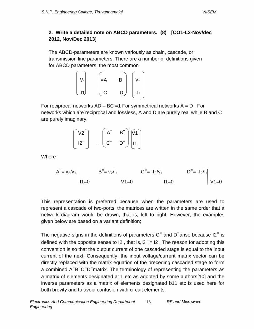
2. Write a detailed note on ABCD parameters. (8) [CO1-L2-Nov/dec 2012, Nov/Dec 2013]
The ABCD-parameters are known variously as chain, cascade, or transmission line parameters. There are a number of definitions given for ABCD parameters, the most common
V1 =A B V2
I1 C D -I2
For reciprocal networks AD – BC =1 For symmetrical networks A = D . For networks which are reciprocal and lossless, A and D are purely real while B and C are purely imaginary.
V2 A‟ B‟ V1
I2‟ = C‟ D‟ I1
Where
A‟= v2/v1 B‟= v2/I1 C‟= -I2/v1 D‟= -I2/I1
I1=0 V1=0 I1=0 V1=0
This representation is preferred because when the parameters are used to represent a cascade of two-ports, the matrices are written in the same order that a network diagram would be drawn, that is, left to right. However, the examples given below are based on a variant definition;
The negative signs in the definitions of parameters C‟ and D‟arise because I2‟ is defined with the opposite sense to I2 , that is,I2‟ = I2 . The reason for adopting this convention is so that the output current of one cascaded stage is equal to the input current of the next. Consequently, the input voltage/current matrix vector can be directly replaced with the matrix equation of the preceding cascaded stage to form a combined A‟B‟C‟D‟matrix. The terminology of representing the parameters as a matrix of elements designated a11 etc as adopted by some authors[10] and the inverse parameters as a matrix of elements designated b11 etc is used here for both brevity and to avoid confusion with circuit elements.

S.K.P. Engineering College, Tiruvannamalai VIISEM
Electronics And Communication Engineering Department 16 RF and Microwave Engineering
3. State and explain the properties of S-Parameters. (16) [CO1-H1-May/June 2013, May/June 2014,April/May 2015]
Zero diagonal elements for perfect matched network.For an ideal network with matched termination Sii=0, since there is no reflection from any port. Therefore under perfect matched condition the diagonal element of [s] are zero. 1) Symmetry of [s] for a reciprocal network
The reciprocal device has a same transmission characteristics in either direction of a pair of ports and is characterized by a symmetric scattering matrix
Sij = Sji ; i≠j
Which results [S] t = [S]
For a reciprocal network with assumed normalized the impeadence matrix equation is [b] = ( [z] + [u] )-1 ([z] – [u]) [a]---------(1) Where u is the unit matrix S matrix equation of etwork is [b] = [s] [a] ------------(2) Compare equ (1) & (2)
[s] =([z]+[u])-1 ([z] – [u]) [R] = [Z] – [U]
[Q] = [Z] + [U]
For a reciprocal network Z matrix Symmetric [R] [Q] = [Q] [R]
[Q] -1[R][Q][Q]-1 = [Q]-1[Q][R][Q]-1
[Q] -1[R] = [R][Q]-1
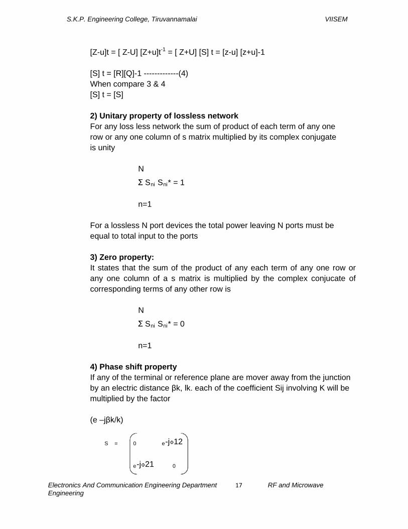
[Q] -1[R] [ S ] = [R][Q]-1 ------------(3) TRANSPOSE OS [s] IS NOW GIVEN AS [S]t = [Z-u]t [ Z+U]t -1
Then
S.K.P. Engineering College, Tiruvannamalai VIISEM
Electronics And Communication Engineering Department 17 RF and Microwave Engineering
[Z-u]t = [ Z-U] [Z+u]t-1 = [ Z+U] [S] t = [z-u] [z+u]-1
[S] t = [R][Q]-1 -------------(4) When compare 3 & 4 [S] t = [S]
2) Unitary property of lossless network For any loss less network the sum of product of each term of any one row or any one column of s matrix multiplied by its complex conjugate is unity
N
Ʃ Sni Sni* = 1
n=1
For a lossless N port devices the total power leaving N ports must be equal to total input to the ports
3) Zero property: It states that the sum of the product of any each term of any one row or any one column of a s matrix is multiplied by the complex conjucate of corresponding terms of any other row is
N
Ʃ Sni Sni* = 0
n=1
4) Phase shift property If any of the terminal or reference plane are mover away from the junction by an electric distance βk, lk. each of the coefficient Sij involving K will be multiplied by the factor
(e –jβk/k)
S = 0 e-jɸ12
e-jɸ21 0

S.K.P. Engineering College, Tiruvannamalai VIISEM
Electronics And Communication Engineering Department 18 RF and Microwave Engineering
4. Formulate S matrix and Compute transmission matrix for a T-network.(16) [CO1-H1-May/June 2013, Nov/Dec 2012]
FORMULATION OF S – PARAMETER
An n-port microwave network has n arms into which power can be fed and
from which power can be taken. In general, power can get from any arm (as input) to any other arm (as output). There are thus n incoming waves and n outgoing waves. We also observe that power can be reflected by a port, so the input power to a single port can partition between all the ports of the network to form outgoing waves. Associated with each port is the notion of a "reference plane" at which the wave amplitude and phase is defined. Usually the reference plane associated with a certain port is at the same place with respect to incoming and outgoing waves. The n incoming wave complex amplitudes are usually designated by the n complex quantities an, and the n outgoing wave complex quantities are designated by the n complex quantities bn. The incoming wave quantities are assembled into an n-vector A and the outgoing wave quantities into an n-vector B. The outgoing waves are expressed in terms of the incoming waves by the matrix equation B = SA where S is an n by n square matrix of complex numbers called the "scattering matrix". It completely determines the behaviour of the network. In general, the elements of this matrix, which are termed "s-parameters", are all frequency-dependent.
For example, the matrix equations for a
2-port are b1 = s11 a1 + s12 a2
b2 = s21 a1 + s22 a2
And the matrix equations for a 3-port are b1 = s11a1+s12a2+s13a3 b2 = s21 a1 + s22 a2 + s23 a3 b3 = s31 a1 + s32 a2 + s33 a3 The wave amplitudes an and bn are obtained from the port current and voltages by the relations a = (V + ZoI)/(2 sqrt(2Zo)) and b = (V - ZoI)/(2 sqrt(2Zo)). Here, a refers to an if V is Vn and I In for the nth port.
S.K.P. Engineering College, Tiruvannamalai VIISEM
Electronics And Communication Engineering Department 19 RF and Microwave Engineering
Note the sqrt(2) reduces the peak value to an rms value, and the sqrt(Zo) makes the amplitude normalised with respect to power, so that the incoming power = aa* and the outgoing power is bb*.
A one-port scattering parameter s is merely the reflection coefficient gamma, and as we have seen we can relate gamma to the load impedance zL = ZL/Zo by the formula gamma = (zL-1)/(zL+1).Similarly, given an n by n "Z-matrix" for an n-port network, we obtain the S matrix from the formula S = (Z-I)(Z+I)^-1, by post-multiplying the matrix (Z-I) by the inverse of the matrix (Z+I). Here, I is the n by n unit matrix. The matrix of z parameters (which has n squared elements) is the inverse of the matrix of y parameters.
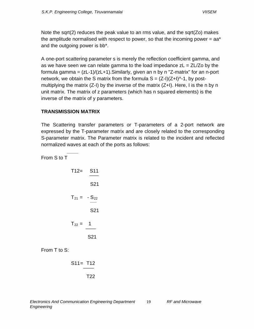
TRANSMISSION MATRIX
The Scattering transfer parameters or T-parameters of a 2-port network are expressed by the T-parameter matrix and are closely related to the corresponding S-parameter matrix. The Parameter matrix is related to the incident and reflected normalized waves at each of the ports as follows: From S to T
T12 = S11
S21
T21 = - S22
S21
T22 = 1
S21
From T to S:
S11 = T12
T22

S.K.P. Engineering College, Tiruvannamalai VIISEM
Electronics And Communication Engineering Department 20 RF and Microwave Engineering
S12 = det(T) Where det(T) is the determinant of matrix
T22
S21 = 1
T22
S22 = - T21
T22
5. Verify the lossless and reciprocity properties of any two port network using scattering matrix. (16) [CO1-H3-Nov/Dec 2014]
Symmetry of [s] for a reciprocal network
The reciprocal device has a same transmission characteristics in either direction of a pair of ports and is characterized by a symmetric scattering matrix
Sij = Sji ; i≠j
Which results
[S] t = [S]
For a reciprocal network with assumed normalized the impeadence matrix equation is [b] = ( [z]
+ [u] )-1 ([z] – [u]) [a] ----------- (1)
Where u is the unit matrix
S matrix equation of network is
[b] = [s] [a] ------------(2)
Compare equ (1) & (2)
[s] =([z]+[u])-1 ([z] – [u])

S.K.P. Engineering College, Tiruvannamalai VIISEM
Electronics And Communication Engineering Department 21 RF and Microwave Engineering
[R] = [Z] – [U]
[Q] = [Z] + [U]
For a reciprocal network Z matrix Symmetric [ R] [Q] = [Q] [R]
[Q] -1[R][Q][Q]-1 = [Q]-1[Q][R][Q]-
1 [Q] -1[R] = [R][Q]-1
[Q] -1[R] [ S ] = [R][Q]-1
For any loss less network the sum of product of each term of any one row or any one column of s matrix multiplied by its complex conjugate is unity
N
Ʃ Sni Sni* = 1 n=1
For a lossless N port devices the total power leaving N ports must be equal to total input to the ports.
6. The S parameters of a two port network are given by
S11=0.2<90° S22=0.2<90°
S12=0.5<90° S21=0.5<0°
(a) Determine whether the network is lossy or not and
(b)Is the network symmetrical and reciprocal? Find the insertion loss of network. [CO1-H1-Nov/Dec 2013, Nov/Dec 2012]
Solution: S11S11*+S21S21*=1
|S11|2+|S21|2=1
(0.2)2+(0.5)=1 0.04+0.25 = 1

S.K.P. Engineering College, Tiruvannamalai VIISEM
Electronics And Communication Engineering Department 22 RF and Microwave Engineering
Therefore the network is not lossless. For symmetrical and reciprocal networks, we can always write as
S11=S22
S12=S21
Since this is symmetrical and reciprocal network Insertion loss = 20log 1
|S12|
= -20log |S12|
= -20log|0.5|
= 6.02dB.
7) Give a detailed note on resistor, inductor and capacitor. (16)
[CO1-L1] o CAPACITOR
o INDUCTOR
o RESISTOR
1. RESISTOR:
The H, Y, Z and ABCD parameters are difficult at microwave frequencies due to the following reasons. (i)Equipment is not readily available to measure total voltage and total current at the ports of the network. (ii) Short circuit and open circuit are difficult to achieve over a wide range of frequencies. (iii) Presence of active devices makes the circuit unstable for short or open circuit. Therefore microwave circuits are analyzed using scattering or S parameters which

S.K.P. Engineering College, Tiruvannamalai VIISEM
Electronics And Communication Engineering Department 23 RF and Microwave Engineering
linearly relate the reflected wave amplitude with those of incident waves.
2. INDUCTOR:
This inductance is exacerbated by the leads of the capacitor, which often dominate the inductance. The inductive parasitics are lumped into a single inductor Ls in series with the capacitor. The finite conductivity of the plates and the leads also results in some series loss, modeled by Rs (sometimes labeled ESR, or effective series resistance). Unless a capacitor is fabricated in a vacuum, the dielectric material that separates the plates also has loss (and resonance), which is usually modeled by a large shunt resistance, Rdi. Furthermore, when a capacitor is soldered onto a PCB, there is parasitic capacitance from the solder pads to the ground plane, resulting in the capacitors, Cp, in the equivalent model. In a like manner, every inductor also has parasitics, as shown in the equivalent circuit model (Fig. 4), which limit operating frequency range. The series resistance, Rx, is due to the winding resistance, and the capacitance Cx models the distributed turn-to-turn capacitance of the windings. The inductor self resonates at a frequency of approximately 1/ √ LCx and has a quality factor Q = ωL/Rx.
When the inductor is soldered onto the PCB, there is an additional capacitance to ground modeled by Cp, which lowers the self-resonant frequency to 1/ p L(Cx + Cp/2).
3. CAPACITOR:
Consider, for instance, a capacitor, which has an equivalent circuit model shown in Fig. 2. The model has many parasitic components which only become relevant at high frequencies. A plot of the impedance of the capacitor, shown in Fig. 3, shows that in addition to the ideal behavior, the most notable difference is the self-resonance that occurs for any real capacitor. The self resonance is inevitable for any real capacitor due to the fact that as AC currents flow through a capacitor, a magnetic field is also generated by the capacitor, which leads to inductance.

S.K.P. Engineering College, Tiruvannamalai VIISEM
Electronics And Communication Engineering Department 24 RF and Microwave Engineering
Unit - II
RF Amplifiers and Matching Networks
Part A
1. Write the function of matching networks? [CO2-L1-Nov/dec-11]
Matching networks can help stabilize the amplifier by keeping the source and load impedances in the appropriate range. Impedance matching (or tuning) is an important issue for - Maximum power is delivered when load is matched to line (assuming the generator is matched) - Power loss is minimized. S/N- ratio of receiver components is increased. - Amplitude and phase errors are reduced.
2. What is function of input and output matching networks? [CO2-L1]
Input and output matching networks are needed to reduce undesired reflections and improve the power flow capabilities.
3. What are the parameters used to evaluate the performance of an amplifier? [CO2-L1]
Key parameters of amplifier, to evaluate the performance are
i. Gain and gain flatness(in dB)
ii. Operating frequency and bandwidth (in Hz)
iii. Output power (in dB)
iv. Power supply requirements (in V and A)
v. Input and output reflection coefficients (VSWR)
vi. Noise figure (in dB)

S.K.P. Engineering College, Tiruvannamalai VIISEM
Electronics And Communication Engineering Department 25 RF and Microwave Engineering
4. Define transducer power gain. [CO2-L1-Nov/dec-13] Transducer power gain is nothing but the gain of the amplifier when placed between source and load.
GT= Power delivered to the load/Available power from the source.
GT=PL/Pavg
5. Define Unilateral Power gain. [CO2-L1-Nov/Dec-14]
It is the amplifier power gain, when feedback effect of amplifier is neglected i.e.S12=0.
GTU = S21
2 (1- ӶS 2) (1- ӶL 2)
(1- ӶS Ӷin)2 (1- S22 ӶL)2
6. What is available Power Gain (GA) at Load? [CO2-L1]
The available power gain for load side matching (TL = T*Out) is given as,
GA= Power available from the network/power available from
the source GA= PN/PA
7. Define Operating Power Gain. [CO2-L1]
The operating power gain is defined as “the ratio of power delivered to the load to the power supplied to the amplifier”.
G= Power delivered to the load/Power supplied to
the amplifier G= PL/Pin
8. Write a short note on feedback of RF circuit. [CO2-L1]
If |T|>1, then the magnitude of the return voltage wave increases called positive feedback, which causes instability (oscillator).
If |T|<1, then the return voltage wave is totally avoided (amplifier). It is called as negative feedback.
S.K.P. Engineering College, Tiruvannamalai VIISEM
Electronics And Communication Engineering Department 26 RF and Microwave Engineering
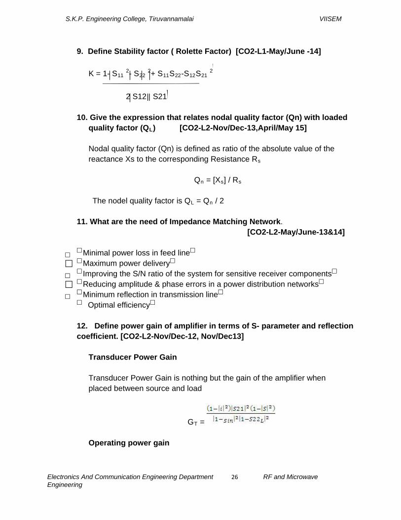
9. Define Stability factor ( Rolette Factor) [CO2-L1-May/June -14]
K = 1- S11 2- S22 2+ S11S22-S12S21 2
2 S12‖ S21
10. Give the expression that relates nodal quality factor (Qn) with loaded
quality factor (QL) [CO2-L2-Nov/Dec-13,April/May 15]
Nodal quality factor (Qn) is defined as ratio of the absolute value of the reactance Xs to the corresponding Resistance Rs
Qn = [Xs] / Rs
The nodel quality factor is QL = Qn / 2
11. What are the need of Impedance Matching Network. [CO2-L2-May/June-13&14]
Minimal power loss in feed line
Maximum power delivery Improving the S/N ratio of the system for sensitive receiver components
Reducing amplitude & phase errors in a power distribution networks Minimum reflection in transmission line
Optimal efficiency
12. Define power gain of amplifier in terms of S- parameter and reflection coefficient. [CO2-L2-Nov/Dec-12, Nov/Dec13]
Transducer Power Gain
Transducer Power Gain is nothing but the gain of the amplifier when placed between source and load
GT =
Operating power gain

S.K.P. Engineering College, Tiruvannamalai VIISEM
Electronics And Communication Engineering Department 27 RF and Microwave Engineering
The Operating power gain is defined as the ratio of power delivered to the load to the power supplied to the amplifier.
GT =
13. What are the considerations in selecting a matching network? [CO2-L1-Nov/Dec12]
(i) Complexity of the system
(ii) Bandwidth requirement
(iii) Adjustability
(iv) Implementation
(v) Maximum power delivery
(vi) Optimal efficiency.
14. Define Stability. [CO2-L1-May/June-14]
Stability refers to the situation where the amplifier remains stable for any passive source and load at the selected frequency and bias condition.
15. State the significance of microstrip matching networks. [CO2-L2-Nov/Dec-14]
(i) Distributed microstrip lines and lumped capacitors
(ii) Less susceptible to parasitic
(iii) Easy to tune
(iv) Efficient PCB implementation
(v) Small size for high frequency.
16. Define noise figure. [CO2-L1-Nov/Dec 2011]
Noise figure F is defined as “the ratio of the input SNR to the output SNR”.

S.K.P. Engineering College, Tiruvannamalai VIISEM
Electronics And Communication Engineering Department 28 RF and Microwave Engineering
F = Input SNR/Output SNR
17. Define unconditional stability [CO2-L1]
It refers to the situation where the amplifier remains stable for any passive source and load at the selected frequency and bias conditions.
18. Mention the advantages of smith chart in the design of matching networks. [CO2-L2] The smith chart allows immediately observing whether or not a particular impedance transformation is capable of achieving the desired matching. Moreover, the total number of possible network configurations can be readily be seen.
19. What is the advantage of T and Pi matching networks? [CO2-L1]
The addition of third element into the two element (L) matching network introduces an additional degree of freedom in the circuit and allows us to control the value of QL by choosing an appropriate intermediate impedance for wider (matching) bandwidth.
20. Why we go for double stub matching networks? [CO2-L2]
(i) They require a variable length transmission line between the stub
and the input port, or between the stub and load impedance.
(ii) Usually this does not a problem for fixed networks, but may create difficulties for variable tuners.

S.K.P. Engineering College, Tiruvannamalai VIISEM
Electronics And Communication Engineering Department 29 RF and Microwave Engineering
PART B
1. Explain the micro strip matching network. (8) [CO2-L2-Nov/Dec -2011,May/June 2014]
Microstrip Line Matching Networks
In the mid-GHz and higher frequency range, the discrete R/L/C lumped
elements will have more noticeable parasitic effects (see chapter 2) and let to complicating the circuit design process
Distributed components such as transmission line segments can be used to mix with lumped elements
From Discrete Components to Microstrip Lines
These type of network usually contain a number of transmission lines connected in series and capacitors spaced in shunt configuration.
Avoid using inductors (if possible) due to higher resistive loss (& higher price)
In general, one shunt capacitor & two series transmission lines is sufficiently to transform any load to any input impedance.
EX: transform load ZL to an input impedance Zin
S.K.P. Engineering College, Tiruvannamalai VIISEM
Electronics And Communication Engineering Department 30 RF and Microwave Engineering
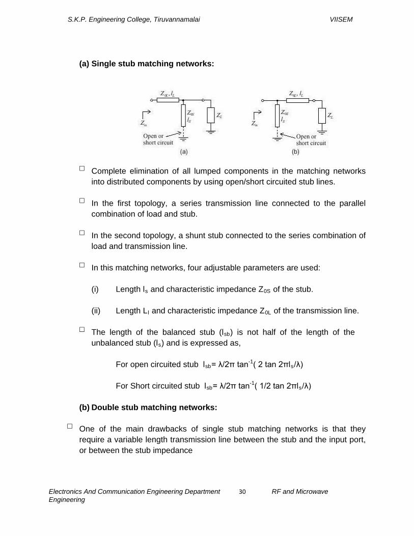
(a) Single stub matching networks:
Complete elimination of all lumped components in the matching networks into distributed components by using open/short circuited stub lines.
In the first topology, a series transmission line connected to the parallel combination of load and stub.
In the second topology, a shunt stub connected to the series combination of load and transmission line.
In this matching networks, four adjustable parameters are used:
(i) Length ls and characteristic impedance Z0S of the stub.
(ii) Length Ll and characteristic impedance Z0L of the transmission line.
The length of the balanced stub (lsb) is not half of the length of the unbalanced stub (ls) and is expressed as,
For open circuited stub lsb= λ/2π tan-1( 2 tan 2πls/λ)
For Short circuited stub lsb= λ/2π tan-1( 1/2 tan 2πls/λ)
(b) Double stub matching networks:
One of the main drawbacks of single stub matching networks is that they
require a variable length transmission line between the stub and the input port, or between the stub impedance

S.K.P. Engineering College, Tiruvannamalai VIISEM
Electronics And Communication Engineering Department 31 RF and Microwave Engineering
In double stub matching, two short or open circuited stubs are connected in shunt with a fixed length transmission line placed in between.
The length l2 of this line is usually chosen to be one-eighth, three eighth or five eighth of a wavelength.
The three eighth or five eighth of a wavelength are typically employed in high frequency applications to simplify the tuner constructions.
2. Discuss the smith chart approach to design the L-section and T- section matching networks (16) [CO2-H3-May/June -13, May/June 14]
S.K.P. Engineering College, Tiruvannamalai VIISEM
Electronics And Communication Engineering Department 32 RF and Microwave Engineering
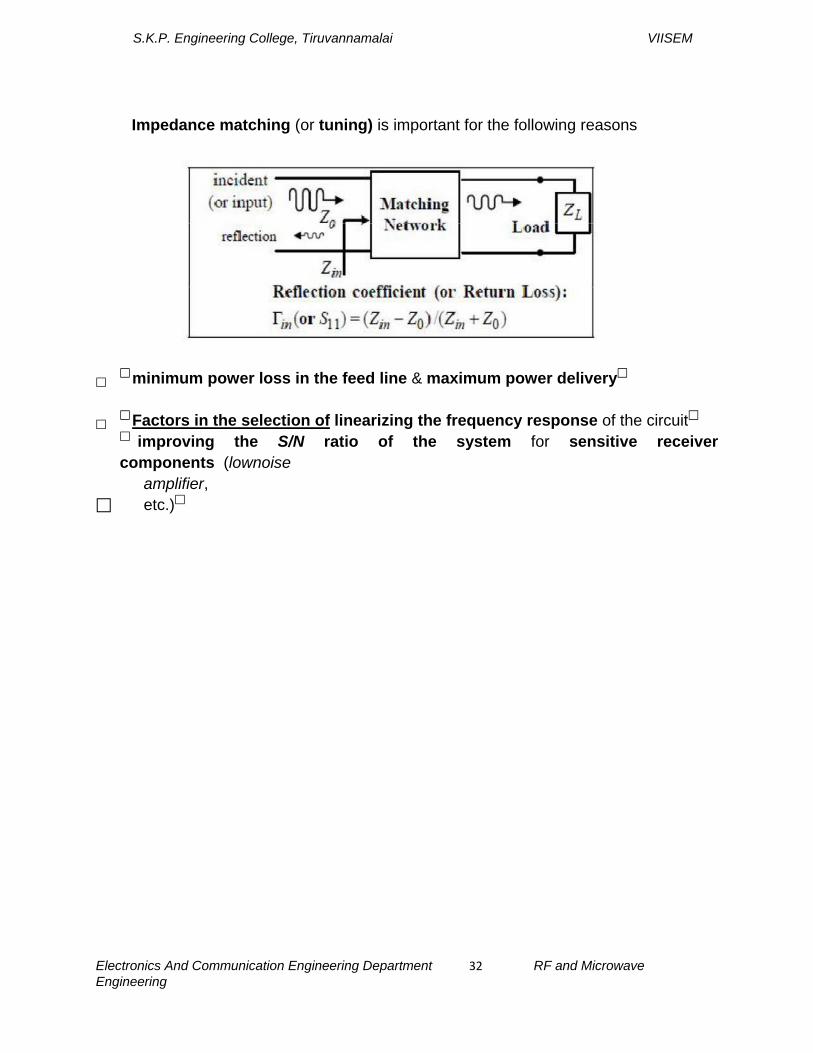
Impedance matching (or tuning) is important for the following reasons
minimum power loss in the feed line & maximum power delivery
Factors in the selection of linearizing the frequency response of the circuit improving the S/N ratio of the system for sensitive receiver components (lownoise
amplifier, etc.)

S.K.P. Engineering College, Tiruvannamalai VIISEM
Electronics And Communication Engineering Department 33 RF and Microwave Engineering
T AND PI MATCHNIG NETWORKS
L-section Networks (Two-component )
(i) Lumped elements: R/L/C
Two component networks are simplest matching networks also known as L
sections or L type networks due to their element arrangements.
These networks use two reactive componens to transform the load impedance Zl to the desired input impedance Zin.
In conjuction with the load and source impedance, the components are alternately connected in series and shunt configuration.

S.K.P. Engineering College, Tiruvannamalai VIISEM
Electronics And Communication Engineering Department 34 RF and Microwave Engineering
Two approaches are used in designing a matching networks.
(i) Derive the valus of elements analytically and
(ii) Rely on the smith chart as a graphical design tool.
The smith chart allows immediately observing whether or not a particular impedance transformation is capable of achieving the desired matching.
(ii) Frequency response For selecting one matching network over other, we are using the following
considerations
(i) DC biasig
(ii) Stability
(iii) Frequency response
(iv) Loaded quality factor (QL)
These networks may be described by a loaded quality factor which is equal
to the ratio of the resonace frequency to the 3 dB Bandwidth. Loaded Quality Factor: QL = fO/BW
If we know the Quality Factor Q, then we can find BW. Estimate Q of matching network using Nodal Quality Factor Qn.
At each circuit node can find Qn = |Xs|/Rs or Qn =|BP|/GP and
QL = Qn/2 true for any L-type Matching Network
The frequency response of these two networks in terms of reflection coefficient is given by,

S.K.P. Engineering College, Tiruvannamalai VIISEM
Electronics And Communication Engineering Department 35 RF and Microwave Engineering
Fig(a): Frequency response of input reflection coefficient
Fig (b): Transfer function of the matching networks.

S.K.P. Engineering College, Tiruvannamalai VIISEM
Electronics And Communication Engineering Department 36 RF and Microwave Engineering
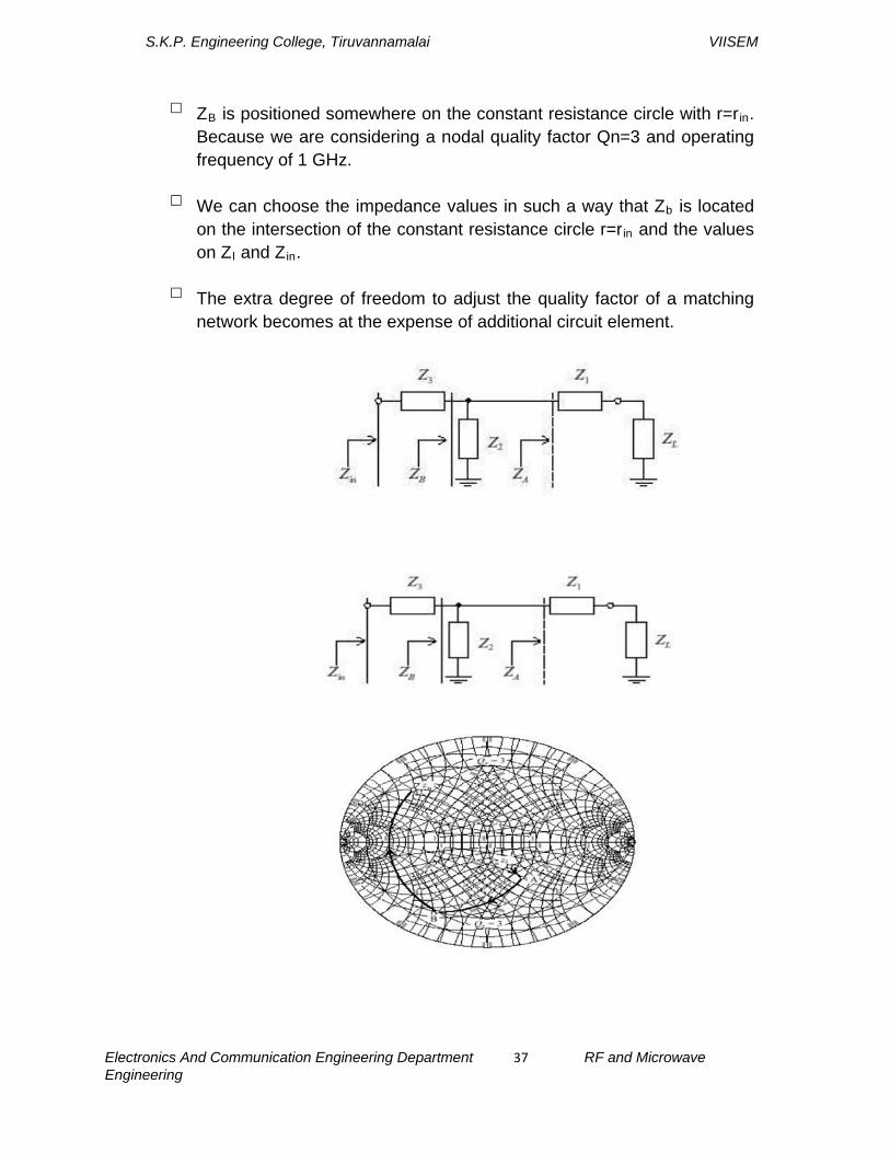
Matching with Lumped Elements: L-section Network
T matching network:
The first element in this network is connected in series with load impedance because Z1 is purely reactive.
The combination of Z1 and Zl are represented as combined impedance ZA.
ZA will reside somewhere on the constant resistance circle in the smith chart described by Ӷ=ӶL
Similarly Z3 is connected in series with the input so that the combined impedance ZB consisting of ZL, Z1, Z2.
S.K.P. Engineering College, Tiruvannamalai VIISEM
Electronics And Communication Engineering Department 37 RF and Microwave Engineering
ZB is positioned somewhere on the constant resistance circle with r=rin. Because we are considering a nodal quality factor Qn=3 and operating frequency of 1 GHz.
We can choose the impedance values in such a way that Zb is located on the intersection of the constant resistance circle r=rin and the values on Zl and Zin.
The extra degree of freedom to adjust the quality factor of a matching network becomes at the expense of additional circuit element.

S.K.P. Engineering College, Tiruvannamalai VIISEM
Electronics And Communication Engineering Department 38 RF and Microwave Engineering
Π Matching network:
The design of Pi-type network is developed with the intent to achieve a
minimum nodal quality factor
A low quality factor design directly translates into a wider bandwidth of a network.

S.K.P. Engineering College, Tiruvannamalai VIISEM
Electronics And Communication Engineering Department 39 RF and Microwave Engineering
3. Microwave amplifier is characterized by its s parameters. Derive
equations for power gain, available gain and transducer gain. (16) [CO2-H1-NOV/DEC-11, Nov/Dec 12, May/June 2013,April/May 2015]
GAIN CONSIDERATION
Consider an arbitrary two-port network, characterized by its scattering matrix [S], connected to source and load impedances ZS and ZL , respectively, as shown in Figure 12.1.
We will derive expressions for three types of power gain in terms of the scattering parameters of the two-port network and the reflection coefficients, _S and _L , of the source and load. Power gain = G = PL/Pin is the ratio of power dissipated in the load ZL to the power delivered to the
input of the two-port network.
This gain is independent of ZS, although the characteristics of some active devices may be dependent on ZS.
Available power gain = GA = Pavn/Pavs is the ratio of the power available from the two-port network to the power available from the source.
This assumes conjugate matching of both the source and the load, and depends on ZS, but not ZL
. _

S.K.P. Engineering College, Tiruvannamalai VIISEM
Electronics And Communication Engineering Department 40 RF and Microwave Engineering
Transducer power gain = GT = PL/Pavs is the ratio of the power delivered to the load to the power available from the source. This depends on both ZS and ZL .
These definitions differ primarily in the way the source and load are matched to the twoport device; if the input and output are both conjugately matched to the two-port device, then the gain is maximized and G =
GA = GT . With reference to Figure 12.1, the reflection coefficient seen looking toward the load
Is = (1a)
while the reflection coefficient seen looking toward the source is
= (1b)
were Z0 is the characteristic impedance reference for the scattering parameters of the two-port network. the following analysis. From the definition of the scattering parameters, and the fact that V+ 2 = _LV− 2 , we have
= (2a)
= (2b)
Eliminating V− 2 from (2a) and solving for V− 1 /V + 1 give
= = = (3a)
where Zin is the impedance seen looking into port 1 of the terminated network. Similarly, the reflection coefficient seen looking into port 2 of the network when port 1 is terminated by ZS is
= = (3b)
By voltage division,
S.K.P. Engineering College, Tiruvannamalai VIISEM
Electronics And Communication Engineering Department 41 RF and Microwave Engineering
= Using from (12.3a) and solving for V+ 1 in terms of VS gives
(4)
If peak values are assumed for all voltages, the average power delivered to the network is
(5)
where (12.4) was used. The power delivered to the load is
(6)
Solving for V−2 from (2b), substituting into (6), and using (4) gives
(7)
The power gain can then be expressed as
G (8)
The power available from the source, , is the maximum power that can be delivered to the network.This occurs when the input impedance of the terminated network is conjugately matched to the source impedance, as discussed in section 2.6. Thus,from (12.5),
= - = (9)
Similarly, the power available from the network, , is the maximum power that can be delivered to the load. Thus from (12.7),

S.K.P. Engineering College, Tiruvannamalai VIISEM
Electronics And Communication Engineering Department 42 RF and Microwave Engineering
= - = | - (10)
In (10),_in must be evaluated for _L=_ out. From (3a), it can be shown that
| - =
(12.10) to
= (11)
Observe that Pavs and Pavn have been expressed in terms of the source voltage, VS, which is independent of the input or load impedances. There would be confusion if these quantities were
expressed in terms of V+ 1 since V+ 1 is different for each of the calculations of PL , Pavs, and
Pavn. Using (12.11) and (12.9), we obtain the available power gain as
= (12)
From (12.7) and (12.9),the transducer power gain is
= (13)
A special case of the transducer power gain occurs when both the input and output are matched for zero reflection (in contrast to conjugate matching). Then _L = _S = 0, and (12.13) reduces to
(14)
S.K.P. Engineering College, Tiruvannamalai VIISEM
Electronics And Communication Engineering Department 43 RF and Microwave Engineering
Another special case is the unilateral transducer power gain, GTU, where S12 = 0 (or is negligibly small). This nonreciprocal characteristic is approximately true for many transistors devices. From (12.3a), in = S11 when S12 = 0, so (12.13) gives the unilateral transducer power gain as
(15)
4. Explain conditional and un conditional stability. (16) [CO2-L2-Nov/Dec2011,April/May 2015]
Unconditional stability: The network is unconditionally stable if[ Гin] <1 and
[Гout]<1 for all passive source and load impedances(i.e Гs<1 and ГL<1)
Conditional stability: The network is conditionally stable if |Гin| < 1 and |Гout| < 1 only for a certain range of passive source and load impedances. This case is also referred to as potentially unstable.
Stability Circles Applying the above requirements for unconditional stability to (3) gives the
following conditions that must be satisfied by _S and _L if the amplifier is to be unconditionally
= + <1
= + <1

S.K.P. Engineering College, Tiruvannamalai VIISEM
Electronics And Communication Engineering Department 44 RF and Microwave Engineering
We can derive the equation for the output stability circle as follows. First use (12.19a) to express the condition that |_in| = 1 as
+ =1 (2)
Now define _ as the determinant of the scattering matrix:
Δ= (3)
Then we can write the above result as
( )+ = (4)
Now square both sides and simplify to obtain
+ (Δ + )=1+ ( + )
( ) ( ) Δ* ) =

S.K.P. Engineering College, Tiruvannamalai VIISEM
Electronics And Communication Engineering Department 45 RF and Microwave Engineering

S.K.P. Engineering College, Tiruvannamalai VIISEM
Electronics And Communication Engineering Department 46 RF and Microwave Engineering
Unit - III
Passive and Active Microwave Devices
Part A
1. What are matched terminators [CO3-L1-May/June-14]
Low power co axial termination Resistance strip
Standard mis matches
2. Name the microwave passive devices which make use of faraday rotation. [CO3-L2-Apr/May-15]
Isolator
Gyrator Circulator
3. What are ferrites? Why its needed in circulator [CO3-L2-Nov/Dec-13], [May/June-14]
Ferrites are non metallic meterials with resistives nearly 10 14 times greater
than metals and also the dielectric constant is in between 10 -15 and relative permeability of the order of 1000
4. Mention the application of gyrator and isolator [CO3-L2-Nov/Dec-14]
Gyrator :
(i) In can be in radar antenna as a duplexer (ii) It will handle a low power . hence they are used as low power devices
Isolator:
(i) Isolator are generally used to improve the frequency stability of microwave generators, such as klystrons and magnetrons in which the reflection from the load affects the generating frequency
5. Define isolator [CO3-L1]

S.K.P. Engineering College, Tiruvannamalai VIISEM
Electronics And Communication Engineering Department 47 RF and Microwave Engineering
An isolator or uniline is two port non reciprocal devices, which produce a minimum attenuation to wave in one direction and very high attenuation in the opposite direction.
6. Draw the Structure of Two hole Directional coupler [CO3-L2-Nov/Dec-11]
7. Draw the diagram for H – plan tee [CO3-L2-Nov/Dec-12]

S.K.P. Engineering College, Tiruvannamalai VIISEM
Electronics And Communication Engineering Department 48 RF and Microwave Engineering
8. What is H-Plane Tee? [CO3-L1]
It is a wave guide tee in which the axis of the slide arm is shunting the E- field or parallel to the H-field of the main guide.
9. Give the applications of directional coupler. [CO3-L2]
1. Unidirectional power measurement
2. SWR measurement
3. Unidirectional wave launching
4. Reflectometer
5. Balanced duplexer.
10. Define directivity of directional coupler. [CO3-L1]
It is defined as a ratio of forward power Pf to the back power Pb
expressed in dB. D(dB)= 10log10 Pf/Pb
It is a measure of how well the directional coupler distinguishes between the forward and reverse travelling powers.
11. What is Gunn Effect? What are the elements that exhibit Gunn Effect?
[CO3-L2-May/june-13]
Gun effect was first observed by GUNN in n_type GaAs bulk diode. According to GUNN, above some critical voltage corresponding to an electric field of 2000-4000v/cm, the current in every specimen became a fluctuating fuction of time. The frequency of oscillation was determined mainly by the specimen and not by the external circuit. The elements are
a) Gallium arsenide b )Indium phosphate c) Cadmium telluride d)Indium arsenide

S.K.P. Engineering College, Tiruvannamalai VIISEM
Electronics And Communication Engineering Department 49 RF and Microwave Engineering
12. What are the factors reducing efficiency of IMPATT diode?[CO3-L2-Nov/Dec 2011]
1) Space charge effect
2) Reverse saturation current effect
3) High frequency skin effect
4) Ionization saturation effect.
13. What is Transferred electron effect? [CO3-L2-Nov/Dec-12]
Some materials like GaAs exhibit negative differential mobility, when biased above a threshold value of the electric field. This behavior is called transferred electron effect. The electrons in the lower energy band will move to the higher energy ban d its called TED.
14. What are the factors reduces the efficiency in Impatt Diode. [CO3-L2] Space charge effect
Reverse saturation current effect
High frequency skin effect
Ionization saturation effect.
15. Mention the ideal characterize of dielectric material in MMIC [CO3-L2-Nov/Dec-13] Small size and Weight
High reliability
Improved reproducibility
Improved performance
Eventual cost reduction when produced in large quantities.
16. What are the necessary condition for Gunn diode. [CO3-L3]

S.K.P. Engineering College, Tiruvannamalai VIISEM
Electronics And Communication Engineering Department 50 RF and Microwave Engineering
This mode is defined in the region when the fL value is about 107 cm/s and the n0/L > 1012 cm2. In this region the device is unstable because of the cyclic formation of either the accumulation layer or the high field domain.
17. List the gunn modes of operations. [CO3-L2]
a. Transit time mode
b. LSA mode
c. Quenched time mode
d. Delayed mode
18. Draw the equivalent circuit for varactor diode [CO3-L2-Apr/may-2015]
19. What are power dividers? [CO3-L1]
Power dividers are used to divide the input power into a number of smaller amounts of power for exciting the radiating elements in an array antenna.
20. What is the principle of Microwave phase shifter? [CO3-L1]
When a wave propagates on a line,a phase difference prevails between any two arbitary points along its paths.The phase difference between two points
21. What are junctions?Give some examples. [CO3-L2]
A microwave circuit consists of several microwave devices connected in some way to achieve the desired transmission of MW signal.The interconnection of two or more microwave may be regarded as MW junction. Eg:Magic Tee,Hybrid Ring
22. What is Tee junction?Give two examples [CO3-L1]
In MW circuits a wave guide or coaxial junction with three independent ports is referred to as tee junction. Eg: E- Plane Tee,H-plane Tee.
23. What is negative resistance in gunn diode? [CO3-L1]

S.K.P. Engineering College, Tiruvannamalai VIISEM
Electronics And Communication Engineering Department 51 RF and Microwave Engineering
The carrier drift velocity increases linearly from 0 to maximum when the electric field is increased from 0 to threshold value in gunndiodes.When the electric field is beyond the threshold value of 3000v/cm the drift velocity is decreased and the diode exhibit negative resistance.
24. Write the applications of magic tee. [CO3-L2]
(i) Measurements of impedance
(ii) As duplexer,
(iii)As mixer
(iv) As an isolator
25. Define coupling factor(C) [CO3-L1]
It is defined as the ratio of incident power Pi to the forward power Pf measured in dB. Coupling factor (dB) = 10log10 Pi/pf.
The coupling factor is a measure of how much of the incident power is being sampled.
PART B
1. Discuss Structure and principle of operation of Isolator. (8) [CO3-L2-Nov/dec-2011,12,13]
An isolator is a nonreciprocal transmission device that is used to isolate one component from reflections of other components in the transmission line. An ideal isolator completely absorbs the power for propagation in one direction and provides lossless transmission in the opposite direction. Thus the isolator is usually called uniline.
Isolators are generally used to improve the frequency stability of microwave generators, such as klystrons and magnetrons, in which the reflection from the load affects the generating frequency. In such cases, the isolator placed between the generator and load prevents the reflected power from the unmatched load from returning to the generator.

S.K.P. Engineering College, Tiruvannamalai VIISEM
Electronics And Communication Engineering Department 52 RF and Microwave Engineering
As a result, the isolator maintains the frequency stability of the generator. Isolators can be constructed in many ways. They can be made by terminating ports 3 and 4 of a four-port circulator with matched loads. On the other hand, isolators can be made by inserting a ferrite rod along the axis of a rectangular waveguide as shown in below.
The isolator here is a Faraday-rotation isolator. Its operating principle can be explained as follows. The input resistive card is in the y-z plane, and the output resistive card is displaced 45° with respect to the input card. The de magnetic field, which is applied longitudinally to the ferrite rod, rotates the wave plane of polarization by 45°. The degrees of rotation depend on the length and diameter of the rod and on the applied de magnetic field. An input TE10 dominant mode is incident to the left end of the isolator. Since the TE10 mode wave is perpendicular to the input resistive card, the wave passes through the ferrite rod without attenuation.
The wave in the ferrite rod section is rotated clockwise by 45° and is normal to the output resistive card. As a result of rotation, the wave arrives at the output end without attenuation at all. On the contrary, a reflected wave from the output end is similarly rotated clockwise 45° by the ferrite rod.
However, since the reflected wave is parallel to the input resistive card, the wave is thereby absorbed by the input card. The typical performance of these isolators is about 1-dB insertion loss in forward transmission and about 20- to 30-dB isolation in reverse attenuation

S.K.P. Engineering College, Tiruvannamalai VIISEM
Electronics And Communication Engineering Department 53 RF and Microwave Engineering
3. Discuss Structure and principle of operation of circulator (16) [CO3-L2-Noc/Dec-2011,12,13,14]
A microwave circulator is a multiport waveguide junction in which the wave can flow only from the nth port to the (n + l)th port in one direction.
Although there is no restriction on the number of ports, the four-port microwave circulator is the most common. One type of four-port microwave circulator is a combination of two 3-dB side-hole directional couplers and a rectangular waveguide with two nonreciprocal phase shifters as shown in Fig
The operating principle of a typical microwave circulator can be analyzed with the aid of Fig. Each of the two 3-dB couplers in the circulator introduces a phase shift of 90°, and each of the two phase shifters produces a certain amount of phase change in a certain direction as indicated.
When a wave is incident to port 1, the wave is split into two components by coupler 1. The wave in the primary guide arrives at port 2 with a relative phase change of 180°. The second wave propagates through the two couplers and the secondary guide and arrives at port 2 with a relative phase shift of 180°. Since the two waves reaching port 2 are in phase, the power transmission is obtained from port 1 to port 2.However, the wave propagates through the primary guide, phase shifter, and coupler 2 and arrives at port 4 with a phase change of 270°. The wave travels through coupler 1 and the secondary guide, and it arrives at port 4 with a phase shift of 90°. Since the two waves reaching port 4 are out of phase by 180°, the power transmission from port 1 to port 4 is zero. In general, the differential propagation constants in the two directions of propagation in a waveguide containing ferrite phase shifters should be

S.K.P. Engineering College, Tiruvannamalai VIISEM
Electronics And Communication Engineering Department 54 RF and Microwave Engineering
ω1- ω3 = (2m+1)π rad/s
ω2- ω4 = 2nπ rad/s
Operating principle:
A microwave circulator is a multiport waveguide junction in which the wave can flow only from the nth port to the (n + l)th port in one direction as shown in fig. Although there is no restriction on the number of ports, the four-port microwave circulator is the most common. One type of four-port microwave circulator is a combination of two 3-dB side-hole directional couplers and a rectangular waveguide with two nonreciprocal phase shifters as shown in Fig.
The operating principle of a typical microwave circulator can be analyzed with the aid of Fig. above. Each of the two 3-dB couplers in the circulator introduces a phase shift of 90°, and each of the two phase shifters produces a certain amount of phase change in a certain direction as indicated.
When a wave is incident to port 1, the wave is split into two components by coupler 1.The wave in the primary guide arrives at port 2 with a relative phase change of 180°. The second wave propagates through the two couplers and the secondary guide and arrives at port 2 with a relative phase shift of 180°.
Since the two waves reaching port 2 are in phase, the power transmission is obtained from port 1 to port 2. However, the wave propagates through the

S.K.P. Engineering College, Tiruvannamalai VIISEM
Electronics And Communication Engineering Department 55 RF and Microwave Engineering
primary guide, phase shifter, and coupler 2 and arrives at port 4 with a phase change of 270°. The wave travels through coupler 1 and the secondary guide, and it arrives at port 4 with a phase shift of 90°. Since the two waves reaching port 4 are out of phase by 180°, the power transmission from port 1 to port 4 is zero.
In general, the differential propagation constants in the two directions of propagation in a waveguide containing ferrite phase shifters should be where m and n are any integers,
including zeros. A similar analysis shows that a wave incident to port 2 emerges at port 3 and so on. As a result, the sequence of power flow is designated as 1 ~ 2 ~ 3 ~ 4 ~ 1. Many types of microwave circulators are in use today.
However, their principles of operation remain the same. Figure 4-6-4 shows a four-port circulator constructed of two magic tees and a phase shifter. The phase shifter produces a phase shift of 180°. The explanation of how this circulator works is left as an exercise for the reader.
S=
S=

S.K.P. Engineering College, Tiruvannamalai VIISEM
Electronics And Communication Engineering Department 56 RF and Microwave Engineering
3. Explain how directional coupler can be used to measure the reflected power. (16) [CO3-H1-Nov/Dec 2012, Nov/ Dec -13,Apr/May -15]
A directional coupler is a four-port waveguide junction as shown in Fig. 4-5-1. It consists of a primary waveguide 1-2 and a secondary waveguide 3-4.
When all ports are terminated in their characteristic impedances, there is free transmission of power, without reflection, between port 1 and port 2, and there is no transmission of power between port 1 and port 3 or between port 2 and port 4 because no coupling exists between these two pairs of ports.
The degree of coupling between port 1 and port 4 and between port 2 and port 3 depends on the structure of the coupler. The characteristics of a directional coupler can be expressed in terms of its coupling factor and its directivity.
Assuming that the wave is propagating from port 1 to port 2 in the primary line, the coupling factor and the directivity are defined,
Where P1 = power input to port 1
P3 = power output from port 3
P4 = power output from port 4
It should be noted that port 2, port 3, and port 4 are terminated in their characteristic impedances.The coupling factor is a measure of the ratio of power levels in the primary and secondary lines.

S.K.P. Engineering College, Tiruvannamalai VIISEM
Electronics And Communication Engineering Department 57 RF and Microwave Engineering
Hence if the coupling factor is known, a fraction of power measured at port 4 may be used to
determine the power input at port
1. This significance is desirable for microwave power measurements because no
disturbance, which may be caused by the power measurements, occurs in the primary line.
2. The directivity is a measure of how well the forward traveling wave in the primary
waveguide couples only to a specific port of the secondary waveguide. An ideal directional coupler should have infinite directivity. In other words, the power at port 3 must be zero because port 2 and port 4 are perfectly matched.
3. Actually, well-designed directional couplers have a directivity of only 30 to 35 dB.
Several types of directional couplers exist, such as a two-hole directional couler, four-hole directional coupler, reverse-coupling directional coupler (Schwinger coupler), and Bethe-hole directional coupler (refer to Fig. 4-5-2). Only the very commonly used two-hole directional coupler is described here.

S.K.P. Engineering College, Tiruvannamalai VIISEM
Electronics And Communication Engineering Department 58 RF and Microwave Engineering
S11 = S22 = S33 = S44 = 0
As noted, there is no coupling between port 1 and port 3 and between port 2 and port 4. Thus
S13 = S31 = S24 = S42 = 0
Consequently, the S matrix of a directional coupler becomes
S=
Equation (4-5-6) can be further reduced by means of the zero property of the S matrix, so we have
S12S*14+S32S*34 = 0
S21S*23+S41S*43 = 0
Also from the unity property of the S matrix, we can write
S12S*12+S14S*14 = 1
Equations (4-5-7) and (4-5-8) can also be written
Since S12 = S21, S14 = S41, S23 = S32 and S34 = S43 Then
Let S12 = S34 = p
Where p is positive and real. Then,
p(S*23+S43) = 0
Let

S.K.P. Engineering College, Tiruvannamalai VIISEM
Electronics And Communication Engineering Department 59 RF and Microwave Engineering
S23 = S41 =jq
where q is positive and real. Then from the above equation p2+q2 = 1 The S matrix of a directional coupler is reduced to
S=
TWO HOLE DIRECTIONAL COUPLERS:
Two-Hole Directional Couplers
A two-hole directional coupler with traveling waves propagating in it is illustrated in Fig. 4-5-3. The spacing between the centers of two holes must be
L = (2n+1)λg/4
A fraction of the wave energy entered into port 1 passes through the holes and is radiated into the secondary guide as the holes act as slot antennas.
The forward waves in the secondary guide are in the same phase, regardless of the hole space, and are added at port 4.

S.K.P. Engineering College, Tiruvannamalai VIISEM
Electronics And Communication Engineering Department 60 RF and Microwave Engineering
The backward waves in the secondary guide (waves are progressing from right to left) are out of phase by (2L/ A8)27T rad and are canceled at port 3.
In a directional coupler all four ports are completely matched. Thus the diagonal elements of the S matrix are zeros 4. Explain the properties of H plane tee and give reasons and why it is called shunt tee. (8) [CO3-H1-NOV /DEC 2012]
An H -plane tee is a waveguide tee in which the axis of its side arm is "shunting" the E field or parallel to the H field of the main guide as shown in Fig.
It can be seen that if two input waves are fed into port 1 and port 2 of the collinear arm, the output wave at port 3 will be in phase and additive. On the other hand, if the input is fed into port 3, the wave will split equally into port 1 and port 2 in phase and in the same magnitude. Therefore the S matrix of the H -plane tee is similar to Eqs.
S13 = S23
S13 = S 23
S33 = 0
S11 = S22
S13 = 1/√2
S11 = ½

S.K.P. Engineering College, Tiruvannamalai VIISEM
Electronics And Communication Engineering Department 61 RF and Microwave Engineering
5. Derive the equation for S matrix of magic TEE. (16) [CO3-H1-NOV /DEC 2012, May / June -13, 14, Nov/ Dec -13]
A magic tee is a combination of the E -plane tee and H -plane tee is called magic tee and it has several characteristics:
1. If two waves of equal magnitude and the same phase are fed into port 1 and port 2, the output will be zero at port 3 and additive at port 4.
2. If a wave is fed into port 4 (the Harm), it will be divided equally between port 1 and port2 of the collinear arms and will not appear at port 3 (the E arm).
3. If a wave is fed into port 3 (the E arm), it will produce an output of equal
magnitude and opposite phase at port 1 and port 2. The output at port 4 is zero. That is, S43 = S34 = 0.
4. If a wave is fed into one of the collinear arms at port 1 or port 2, it will not appear
in the other collinear arm at port 2 or port 1 because the E arm causes a phase delay while the Harm causes a phase advance. That is, S,z = Sz1 = 0.
Therefore the S matrix of a magic tee can be expressed as
The magic tee is commonly used for mixing, duplexing, and impedance measurements. Suppose, for example, there are two identical radar transmitters in equipment stock.
A particular application requires twice more input power to an antenna than either transmitter can deliver. A magic tee may be used to couple the two transmitters to the antenna in such a way that the transmitters do not load each other.
The two transmitters should be connected to ports 3 and 4, respectively, as shown in Fig.above. Transmitter 1, connected to port 3, causes a wave to emanate from port 1 and another to emanate from port 2; these waves are equal in magnitude but opposite in phase.

S.K.P. Engineering College, Tiruvannamalai VIISEM
Electronics And Communication Engineering Department 62 RF and Microwave Engineering
Similarly, transmitter 2, connected to port 4, gives rise to a wave at port 1 and another at port 2, both equal in magnitude and in phase.
At port 1 the two opposite waves cancel each other. At port 2 the two in-phase waves add together; so double output power at port 2 is obtained for the antenna as shown in Fig.
S=
But S21 = 0, S12 = 0, S43 = 0, S34 = 0
S11 = 0, S22 = 0, S33 = 0, S44 = 0
S14 = S24, S13 = -S23
For port-3 and port-4 matched, the S matrix becomes
S=
S=
S=
6. Explain the properties of E plane Tee? derive the expression for scattering matrix. [CO3-L2-May/june -2013,Nov/Dec -14] An E -plane tee is a waveguide tee in which the axis of its side arm is parallel to theE field of the main guide

S.K.P. Engineering College, Tiruvannamalai VIISEM
Electronics And Communication Engineering Department 63 RF and Microwave Engineering
If the collinear arms are symmetric about the side arm, there are two different transmission characteristics
It can be seen from Fig. 4-4-4 that if the Eplane tee is perfectly matched with the aid of screw tuners or inductive or capacitive windows at the junction, the diagonal components of the scattering matrix, S1~,Szz, and S33, are zero because there will be no reflection.
When the waves are fed into the side arm (port 3), the waves appearing at port 1 and port 2 of the collinear arm will be in opposite phase and in the same magnitude. Therefore It should be noted that Eq.does not mean that SI3 is always positive andS23 is always negative. The negative sign merely means that Sl3 and S23 have opposite signs. For a matched junction, the S matrix is given by
S= (a)
From the symmetry property of S matrix, the symmetric terms in Eq. ( a ) are equal and they are
S12 = S21, S13 = S31, S23 = S32 (b)
From the zero property of S matrix, the sum of the products of each term of any column (or row) multiplied by the complex conjugate of the corresponding terms of any other column (or row) is zero and it is

S.K.P. Engineering College, Tiruvannamalai VIISEM
Electronics And Communication Engineering Department 64 RF and Microwave Engineering
S11S12+S22S*22+S31S*32 = 0 (c)
Hence
S13S*13 = 0 (d)
This means that either Sl3 or St3, or both, should be zero. However, from the unity property of S matrix, the sum of the products of each term of any one row (or column) multiplied by its complex conjugate is unity; that is,
S21S*21+S31S*31 = 1 (e)
S12S*12+S32S*32 (f)
S13S*13+S23S*23 = 1 (g)
Substitution of Eq. ( b) in ( e) results in
(h)
zero and thus Eq. ( g) is false. In a similar fashion, if S23 = 0, then S 13 becomes zero and therefore Eq.(h) is not true.
This inconsistency proves the statement that the tee junction cannot be matched to the three arms. In other words, the diagonal elements of the S matrix of a tee junction are not all zeros.
In general, when an £-plane tee is constructed of an empty waveguide, it is poorly matched at the tee junction. Hence SiJ * 0 if i = j.
However, since the collinear arm is usually symmetric about the side arm, I S13l = I S23l and S11 = S22. Then the S matrix can be simplified to
S= (i)
S.K.P. Engineering College, Tiruvannamalai VIISEM
Electronics And Communication Engineering Department 65 RF and Microwave Engineering
7. With neat diagram , explain the working principle of Gunn diode mention its
application.(16) [CO3-L2-Nov/Dec 2011,2012,2013,14,May/June – 13,14,April/May 15]
Gunn Effect:
Gun effect was first observed by GUNN in n_type GaAs bulk diode. According to GUNN, above some critical voltage corresponding to an electric field of 2000-4000v/cm, the current in every specimen became a fluctuating fuction of time. The frequency of oscillation was determined mainly by the specimen and not by the external circuit.
RIDLEY-WATKINS-HILSUM (RWH THEORY
Differential Negative Resistance
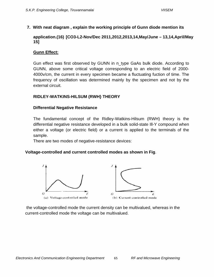
The fundamental concept of the Ridley-Watkins-Hilsum (RWH) theory is the differential negative resistance developed in a bulk solid-state Ill-Y compound when either a voltage (or electric field) or a current is applied to the terminals of the sample. There are two modes of negative-resistance devices:
Voltage-controlled and current controlled modes as shown in Fig.
the voltage-controlled mode the current density can be multivalued, whereas in the current-controlled mode the voltage can be multivalued.

S.K.P. Engineering College, Tiruvannamalai VIISEM
Electronics And Communication Engineering Department 66 RF and Microwave Engineering
The major effect of the appearance of a differential negative-resistance region in the currentdensity-field curve is to render the sample electrically unstable. As a result, the initially homogeneous sample becomes electrically heterogeneous in an attempt to reach stability.
In the voltage-controlled negative-resistance mode high-field domains are formed, separating two low-field regions. The interfaces separating lowand high-field domains lie along equipotentials; thus they are in planes perpendicular to the current direction as shown in Fig. (a). In the current-controlled negative-resistance mode splitting the sample results in high-current filaments running along the field direction as shown in Fig. (b).
Expressed mathematically, the negative resistance of the sample at a particular region is
= negative resistance (1)
If an electric field Eo (or voltage Vo) is applied to the sample, for example, the current density is generated. As the applied field (or voltage) is increased to E2 (or V2), the current density is decreased to J2.
When the field (or voltage) is decreased to E1 (or V1), the current density is increased to J1 . These phenomena of the voltage controlled negative resistance are shown in Fig. 7-2-3(a).
Similarly, for the current controlled mode, the negative-resistance profile is as shown in Fig. 7-2-3(b).

S.K.P. Engineering College, Tiruvannamalai VIISEM
Electronics And Communication Engineering Department 67 RF and Microwave Engineering
Two-Valley Model Theory
According to the energy band theory of then-type GaAs, a high-mobility lower valley is separated by an energy of 0.36 eV from a low-mobility upper valley
When the applied electric field is lower than the electric field of the lower valley (£ < Ec), no electrons will transfer to the upper valley as show in Fig. 7-2-S(a).
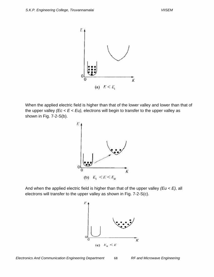
S.K.P. Engineering College, Tiruvannamalai VIISEM
Electronics And Communication Engineering Department 68 RF and Microwave Engineering
When the applied electric field is higher than that of the lower valley and lower than that of the upper valley (Ec < E < Eu), electrons will begin to transfer to the upper valley as shown in Fig. 7-2-S(b).
And when the applied electric field is higher than that of the upper valley (Eu < E), all electrons will transfer to the upper valley as shown in Fig. 7-2-S(c).

S.K.P. Engineering College, Tiruvannamalai VIISEM
Electronics And Communication Engineering Department 69 RF and Microwave Engineering
If electron densities in the lower and upper valleys are nc and nu , the conductivity of the n -type GaAs is
(2)
Where
E = electron charge electron mobility
n= nl+ nu is the electron density
When a sufficiently high field E is applied to the specimen, electrons are accelerated and their effective temperature rises above the lattice temperature. Furthermore, the lattice temperature also increases. Thus electron density n and mobility f-L are both functions of electric field E. Differentiation of Eq. (7-2-2) with respect toE yields
(3)
If the total electron density is given by n = nt + nu and it is assumed that f.Le and /Lu are proportional to
EP, where p is a constant, then
(4)
(5)
(6)
Substitution of Eqs. (4) to (6) into Eq. (3) results in

S.K.P. Engineering College, Tiruvannamalai VIISEM
Electronics And Communication Engineering Department 70 RF and Microwave Engineering
(7) Then differentiation of Ohm's law J = aE with respect toE yields
(8)
Equation (8) can be rewritten
(9)
Clearly, for negative resistance, the current density J must decrease with increasing field E or the ratio of dJ!dE must be negative. Such would be the case only if the right-hand term of Eq. (9) is less than zero. In other words, the condition for negative resistance is
- (10)
8. Draw the construction and explain the working of IMPATT diode. (16) [CO3-L2-Nov/Dec - 12,May/June -13,April/May 15]
Physical Structures
A theoretical Read diode made of ann+ -p-i-p+ or p+ -n-i-n+ structure has been analyzed. Its basic physical mechanism is the interaction of the impact ionization avalanche and the transit time of charge carriers. Hence the Read-type diodes are called IMPATT diodes. These diodes exhibit a differential negative resistance by two effects:
1)The impact ionization avalanche effect, which causes the carrier current lo(t) and the ac voltage to be out of phase by 90°
2) The transit-time effect, which further delays the external current l,(t) relative to the ac voltage by 90°
The first IMPATT operation as reported by Johnston et al. [4] in 1965, however, was obtained from a simple p-n junction. The first real Read-type IMPATT diode was reported by Lee et al. [3], as described previously.

S.K.P. Engineering College, Tiruvannamalai VIISEM
Electronics And Communication Engineering Department 71 RF and Microwave Engineering
From the small-signal theory developed by Gilden [5] it has been confirmed that a negative resistance of the IMPATT diode can be obtained from a junction diode with any doping profile.
Many IMPATT diodes consist of a high doping avalanching region followed by a drift region where the field is low enough that the carriers can traverse through it without avalanching.
The Read diode is the basic type in the IMPATT diode family. The others are the one-sided abrupt p-n junction, the linearly graded p-n junction (or double-drift region), and the p-i-n diode, all of which are shown in Fig. 8-2-1.
Negative Resistance
Small-signal analysis of a Read diode results in the following expression for the real part of the diode terminal impedance [5]:

S.K.P. Engineering College, Tiruvannamalai VIISEM
Electronics And Communication Engineering Department 72 RF and Microwave Engineering
Moreover, () is the transit angle, given by
(2)
and w, is the avalanche resonant frequency, defined by
(3)

S.K.P. Engineering College, Tiruvannamalai VIISEM
Electronics And Communication Engineering Department 73 RF and Microwave Engineering
The variation of the negative resistance with the transit angle when w > Wr is plotted in Fig. 8-2-2. The peak value of the negative resistance occurs near () = 7T. For transit angles larger than 7T and
approaching 37T /2, the negative resistance of the diode decreases rapidly. For practical purposes, the Read-type IMPATT diodes work well only in a frequency range around the 7T transit angle. That is,
f = (4)
Power Output and Efficiency
For a uniform avalanche, the maximum voltage that can be applied across the diode is given by
(5)
where
Lis the depletion length
Em is the maximum electric field.
This maximum applied voltage is limited by the breakdown voltage. Furthermore, the maximum current that can be carried by the diode is also limited by the avalanche breakdown process, for the current in the space-charge region causes an increase in the electric field. The maximum current is given by

S.K.P. Engineering College, Tiruvannamalai VIISEM
Electronics And Communication Engineering Department 74 RF and Microwave Engineering
(6)
Therefore the upper limit of the power input is given by
= (7)
The capacitance across the space-charge region is defined as
C = (8)
Substitution of Eq. (8-2-8) in Eq. (8-2-7) and application of 2TTfT = 1 yield
(9)
It is interesting to note that this equation is identical to Eq. (5-1-60) of the power frequency limitation for the microwave power transistor. The maximum power that can be given to the mobile carriers decreases as 1/ f. For silicon, this electronic limit is dominant at frequencies as high as 100 GHz. The efficiency of the IMPATT diodes is given by η and equation as follows.
(10)
9. Explain in detail with suitable diagrams the fabrication techniques of a monolithic
MICROWAVE MONOLITHIC INTEGRATED CIRCUITES
The metal-oxide-semiconductor field-effect transistor (MOSFET) is a four-terminal device. There are both n-channel and p-channel MOSFETs. The n-channel MOSFET consists of a slightly doped p -type semiconductor substrate into which two highly doped n + sections are diffused, as shown in Fig.
These n + sections, which act as the source and the drain, are separated by about 0.5 f.Lm. A thin layer of insulating silicon dioxide (Si02) is grown over the surface of the structure. The metal contact on the insulator is called the gate. Similarly, the p -channel MOSFET is made of a slightly doped n -type semiconductor with two highly doped p +-type regions for the source and drain. The heavily doped polysilicon or a combination of silicide and polysilicon can also be used as the gate electrode. In
Integrated Circuits. (16) [CO3-L2]

S.K.P. Engineering College, Tiruvannamalai VIISEM
Electronics And Communication Engineering Department 75 RF and Microwave Engineering
practice, a MOSFET is commonly surrounded by a thick oxide to isolate it from the adjacent devices in a microwave integrated circuit. The basic device parameters of a MOSFET are as follows: L is the channel length, which is the distance between the two n+ -p junctions just beneath the insulator (say, 0.5 JLm), Z is the channel depth (say, 5JLm), dis the insulator thickness (say, 0.1 JLm), and r1 is the junction thickness of then+ section (say, 0.2 JLm).
MATERIALS AND FABRICATION TECHNIQUES
1. n-Channel Enhancement Mode (normally OFF). When the gate voltage is zero, the channel conductance is very low and it is not conducting. A positive voltage must be applied to the gate to form an n channel for conduction. The drain current is enhanced by the positive voltage. This type is called the enhancement-mode (normally OFF) n-channel MOSFET.
n-Channel Depletion Mode (normally ON). If an n channel exists at equilibrium (that is, at zero bias), a negative gate voltage must be applied to deplete the carriers in the channel. In effect, the channel conductance is reduced, and the device is turned OFF. This type is called the depletion-mode (normally ON) n-channel MOSFET. p -Channel Enhancement Mode (normally OFF). A negative voltage must be applied to the gate to induce a p channel for conduction. This type is called the enhancement-mode (normally OFF) p-channel MOSFET.

S.K.P. Engineering College, Tiruvannamalai VIISEM
Electronics And Communication Engineering Department 76 RF and Microwave Engineering
p -Channel Depletion Mode (normally ON). A positive voltage must be applied to the gate to deplete the carriers in the channel for nonconduction. This type is called the depletion-mode (normally ON) p-channel MOSFET.

S.K.P. Engineering College, Tiruvannamalai VIISEM
Electronics And Communication Engineering Department 77 RF and Microwave Engineering
Unit - IV
Microwave Generation
Part A
1. What is the role of slow wave structure in TWT? [CO4-L1-May/June 2013,May/June 14]
Slow wave structure are a special circuits that are used in microwave tubes to reduce the wave velocity in a certain direction so that the electron beam and the signal were interact
2. Compare M and O type tubes. [CO4-L2-Nov/Dec-12] M type Tubes O type Tubes Static magnetic field is same Static magnetic field is perpendicular direction to the electric field to the electric field
Klystron and TWT are the O type
Magnetron is the M type Tube Tubes Electron travel in curved path Electron travel in linear path
3. Compare TWT & Klystron. [ CO4-L2- Nov/Dec 2013] Klystron Amplifier TWTA Linear beam or O type tubes Linear beam or O type tubes Uses a cavities for input and output Uses non resonant wave circuit
Circuits

S.K.P. Engineering College, Tiruvannamalai VIISEM
Electronics And Communication Engineering Department 78 RF and Microwave Engineering
Wide band device because use of
Narrow band device duo to use of non-
resonant cavities resonant circuit
4. What are the limitation in conventional vacuum tubes.[CO4-L1-Apr/May -15]
The concentional tubes such as triode, tetrodes, pentodes can be used as amplifiers and oscillators more efficiently. But these conventional tubes can not used as amplifier or oscillator at high frequency (>1000MHZ) because at higher frequencies output drops off The factors of contributing of output at UHF are
Circuit resistance
a) Inter electrode capacitance
b) Lead inductance
Transit time effects
Cathode emission plate heat dissipation area
Power loss due to skin effect, radiation and dielectric loss Gain band width product
5. Define convection current in TWT. [CO4-L1-May/June-14]
The convection current induced in the electron beam is by the axial electric field. When the space charge effect is considered, the electron velocity, charge density, current density and the axial electric field will perturbate about their averages or DC values.
I= jβe I0E1/2vo(jβe-γ2)

S.K.P. Engineering College, Tiruvannamalai VIISEM
Electronics And Communication Engineering Department 79 RF and Microwave Engineering
6. Define resonant frequency. [CO4-L1]
Resonant frequency fr at which the energy in the cavity attains maximum value=2We or 2Wm.
7. What are the drawbacks available in klystron? [CO4-L2]
(i) Klystrons are essentially narrowband devices
(ii) In klystrons and magnetrons, the microwave circuit consists
of a resonant structures which limits the BW of the tube.
8. What is TWTA? [CO4-L1]
A travelling wave tube amplifier (TWTA) circuit uses a helix slow wave non resonant microwave guiding structures. It is a bradband devices.
9. State the characteristics of TWTA. [CO4-L2]
Frequency range: 3GHz and higher
Bandwidth: about 0.8GHz
Efficiency: 20 to 40%
Power output: upto 10Kw average
Power gain: upto 60dB
10. State the applications of TWT. [CO4-L2]
(i) Microwave power satellite
(ii) Higher power satellite transponder output and
(iii) Radar transmitters.
11. What are the advantages of TWT? [CO4-L2]
(i) BW is large

S.K.P. Engineering College, Tiruvannamalai VIISEM
Electronics And Communication Engineering Department 80 RF and Microwave Engineering
(ii) High Reliability
(iii) High gain
(iv) Higher duty cycle.
12. Name four types of slow wave structures. [CO4-L2]
(i) Helical line
(ii) Folded back line
(iii) Zigzag line and
(iv) Inter digital line.
13. Define Velocity modulation. [CO4-L1]
The variation in electron velocity in the drift space is known as velocity modulation.
14. Define bunching. [CO4-L1]
The electrons passing the first cavity gap at zeros of the gap voltage pass through with unchanged velocity, those passing through the positive half cycles of gap voltage undergo an increase in velocity; those passing through the negative half cycle of gap voltage undergo an increase in velocity. As a result of these, electrons bunch together in drift space. This is called bunching.
15. State the power gain,power output and efficiency of two cavity
klystron amplifier. [CO4-L2]
(i) Efficiency: about 40%
(ii) Power output: Average power is upto 500KW and pulsed power is upto 30MW at 10GHz.
(iii) Power gain: about 30dB.

S.K.P. Engineering College, Tiruvannamalai VIISEM
Electronics And Communication Engineering Department 81 RF and Microwave Engineering
16. What are the assumptions for calculation of RF power in Reflex Klystron? [CO4-L1]
i) Cavity grids and repeller are plane parallel and very large in extent.
ii) No RF field is excited in repeller space
iii) Electrons are not intercepted by the cavity anode grid.
iv) No debunching takes place in repeller space.
v) The cavity RF gap voltage amplitude V, is small compared to the dc beam
voltage VO
17. What is the condition for oscillation in Reflex klystron? [CO4-L1]
The necessary condition for oscillation is that the magnitude of the negative real
part of the electronic admittance should not be less than the total conductance of the cavity circuit i.e. –Ge ≥G.
Where G=Gc + Gb +G1 = 1/ Rsh Rsh - effective shunt resistance Gc - copper losses of cavity Gb- beam loading conductance G1 - load conductance
18. What is the effect of transit time? [CO4-L1]
There are two effects.
1) At low frequencies, the grid and anode signals are no longer 180O out of phase, thus causing design problems with feedback in oscillators.
2) The grid begins to take power from the driving source and the power is absorbed even when the grid is negatively biased.
19. What are the applications of reflex klystron? [CO4-L1]
1) Signal source in MW generator 2) Local oscillators in receivers 3) It is used in FM oscillator in low power MW links.

S.K.P. Engineering College, Tiruvannamalai VIISEM
Electronics And Communication Engineering Department 82 RF and Microwave Engineering
4) In parametric amplifier as pump source
20. How the klystron amplifier can act as klystron oscillator? [CO4-L2]
When the klystron amplifier is given a positive feedback such that the overall phase shift becomes zero 360° and Av = I then klystron amplifier acts as an oscillator.
21. Define Transit time in Reflex klystron. [CO4-L1]
The time taken by the electron to travel into the repeller space and back to the gap.
T =n + ¾
22. Write the parameters on which bunching depend on. [CO4-L2] i) Drift space should be properly adjusted.
ii) D.C anode voltage
iii) Signal amplitude should be such that proper bunching takes place.
23. State the characteristics of magnetron and of 2-cavity klystron amplifier. [CO4-L1]
Magnetron:
Operating frequencies 70 GH z
Output power 40 MW
Efficiency 40 to 70%
2-cavity klystron:
Efficiency 40%
Power output average power 500 KW
Pulsed power 30 MW
Power gain about 30 db.

S.K.P. Engineering College, Tiruvannamalai VIISEM
Electronics And Communication Engineering Department 83 RF and Microwave Engineering
24. What is meant by strapping? [CO4-L1]
The magnetron has eight or more coupled cavity resonators and hence several modes of oscillation are possible. The oscillating frequency of different modes are not same and are quite close to each other which results in mode jumping. i.e., a 3 cm π mode oscillation which is normal for a particular magnetron Could become a 3.05 cm 3/4 mode oscillation. This result in oscillations of reduced power at wrong frequency. To prevent this. Strapping is used. It consists of two rings of heavy gauge wire connecting alternate anode poles. It provides a phase difference
0f 2 π radians for the modes other π-mode and thus preventing the occurrence of other modes, except the π-mode .
25. State the applications of magnetrons. [CO4-L2]
1) Pulse work in radar 2) Linear particle accelerators. 3) Radar transmitters 4) Microwave ovens
26. What is frequency pulling and frequency pushing in magnetrons? [CO4-L1]
Frequency pulling is caused by changes in the load impedance reflected into the cavity resonators. Frequency pushing is due to the change in anode voltage which alters the orbital velocity of electron clouds.
27. Define electronic efficiency. [CO4-L1]
The electronic efficiency of the klyston amplifier is defined as the ration of the output power to the input power.
Efficiency: Pout/Pin = β0I2V2/2I0V0
28. What is hull cutoff condition? [CO4-L1]
In a magnetron, the electron will just graze the anode and return towards the cathode depends on Vo and Bo . The hull cut of magnetic equation is Boc = (8Vo m / e) ½ / b(1- a 2 / b2 )
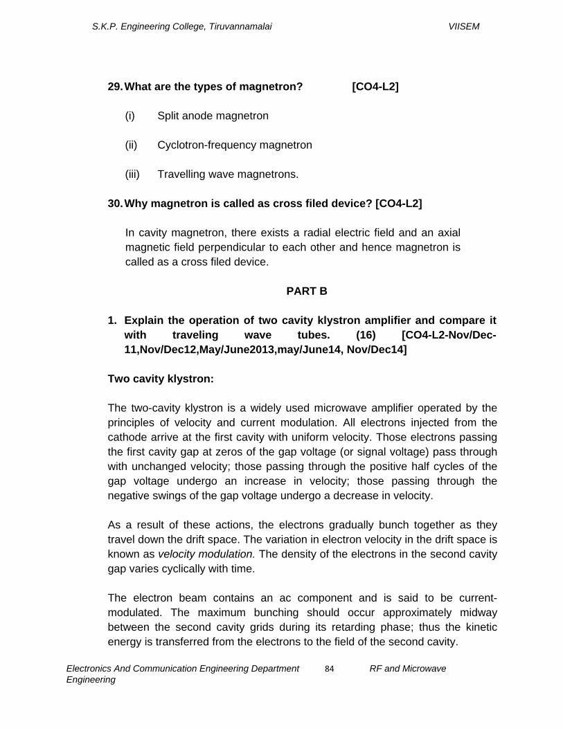
S.K.P. Engineering College, Tiruvannamalai VIISEM
Electronics And Communication Engineering Department 84 RF and Microwave Engineering
29. What are the types of magnetron? [CO4-L2]
(i) Split anode magnetron
(ii) Cyclotron-frequency magnetron
(iii) Travelling wave magnetrons.
30. Why magnetron is called as cross filed device? [CO4-L2]
In cavity magnetron, there exists a radial electric field and an axial magnetic field perpendicular to each other and hence magnetron is called as a cross filed device.
PART B
1. Explain the operation of two cavity klystron amplifier and compare it
with traveling wave tubes. (16) [CO4-L2-Nov/Dec-11,Nov/Dec12,May/June2013,may/June14, Nov/Dec14]
Two cavity klystron:
The two-cavity klystron is a widely used microwave amplifier operated by the principles of velocity and current modulation. All electrons injected from the cathode arrive at the first cavity with uniform velocity. Those electrons passing the first cavity gap at zeros of the gap voltage (or signal voltage) pass through with unchanged velocity; those passing through the positive half cycles of the gap voltage undergo an increase in velocity; those passing through the negative swings of the gap voltage undergo a decrease in velocity.
As a result of these actions, the electrons gradually bunch together as they travel down the drift space. The variation in electron velocity in the drift space is known as velocity modulation. The density of the electrons in the second cavity gap varies cyclically with time.
The electron beam contains an ac component and is said to be current-modulated. The maximum bunching should occur approximately midway between the second cavity grids during its retarding phase; thus the kinetic energy is transferred from the electrons to the field of the second cavity.
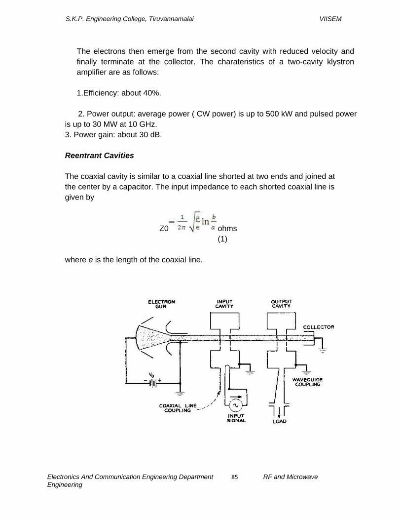
S.K.P. Engineering College, Tiruvannamalai VIISEM
Electronics And Communication Engineering Department 85 RF and Microwave Engineering
The electrons then emerge from the second cavity with reduced velocity and finally terminate at the collector. The charateristics of a two-cavity klystron amplifier are as follows:
1.Efficiency: about 40%.
2. Power output: average power ( CW power) is up to 500 kW and pulsed power is up to 30 MW at 10 GHz. 3. Power gain: about 30 dB.
Reentrant Cavities
The coaxial cavity is similar to a coaxial line shorted at two ends and joined at the center by a capacitor. The input impedance to each shorted coaxial line is given by
Z0 ohms (1)
where e is the length of the coaxial line.
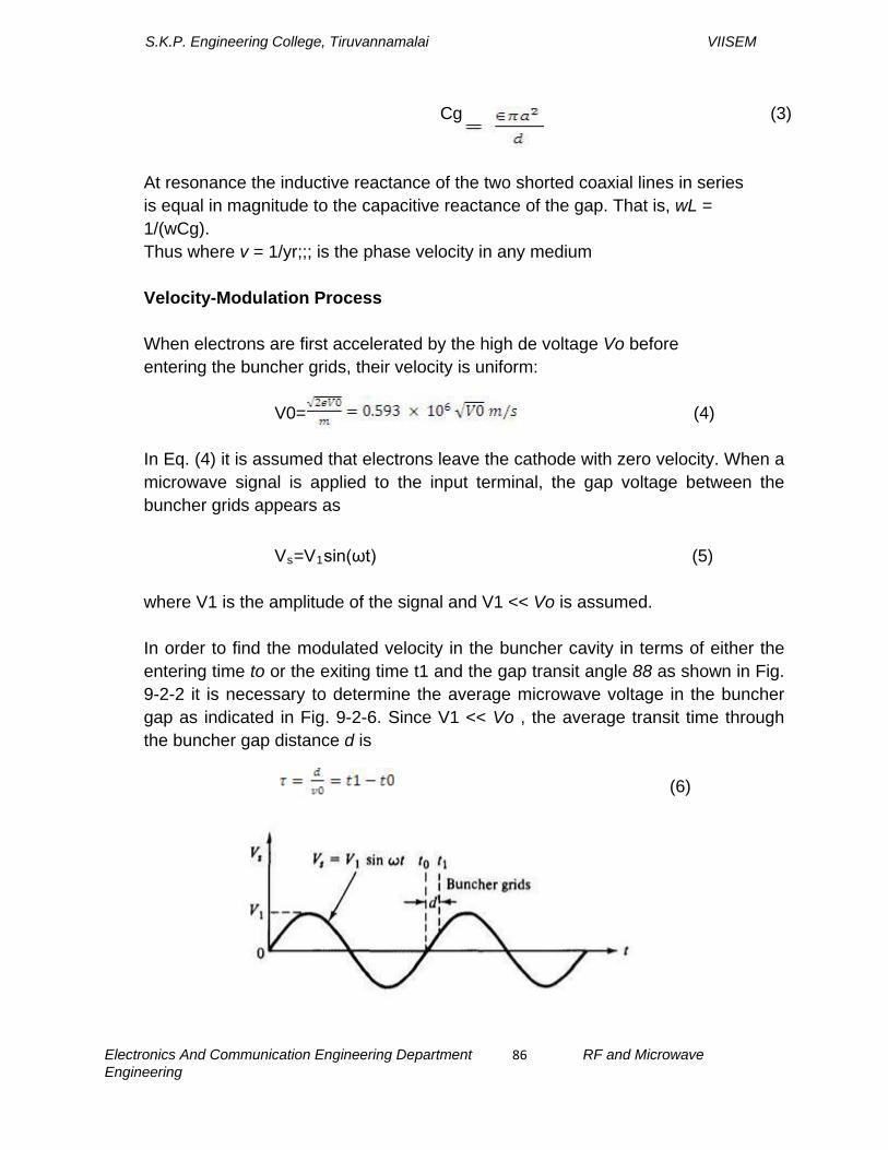
S.K.P. Engineering College, Tiruvannamalai VIISEM
Electronics And Communication Engineering Department 86 RF and Microwave Engineering
Cg (3)
At resonance the inductive reactance of the two shorted coaxial lines in series is equal in magnitude to the capacitive reactance of the gap. That is, wL = 1/(wCg). Thus where v = 1/yr;;; is the phase velocity in any medium
Velocity-Modulation Process
When electrons are first accelerated by the high de voltage Vo before entering the buncher grids, their velocity is uniform:
V0= (4)
In Eq. (4) it is assumed that electrons leave the cathode with zero velocity. When a microwave signal is applied to the input terminal, the gap voltage between the buncher grids appears as
Vs=V1sin(ωt) (5)
where V1 is the amplitude of the signal and V1 << Vo is assumed.
In order to find the modulated velocity in the buncher cavity in terms of either the entering time to or the exiting time t1 and the gap transit angle 88 as shown in Fig. 9-2-2 it is necessary to determine the average microwave voltage in the buncher gap as indicated in Fig. 9-2-6. Since V1 << Vo , the average transit time through the buncher gap distance d is
(6)
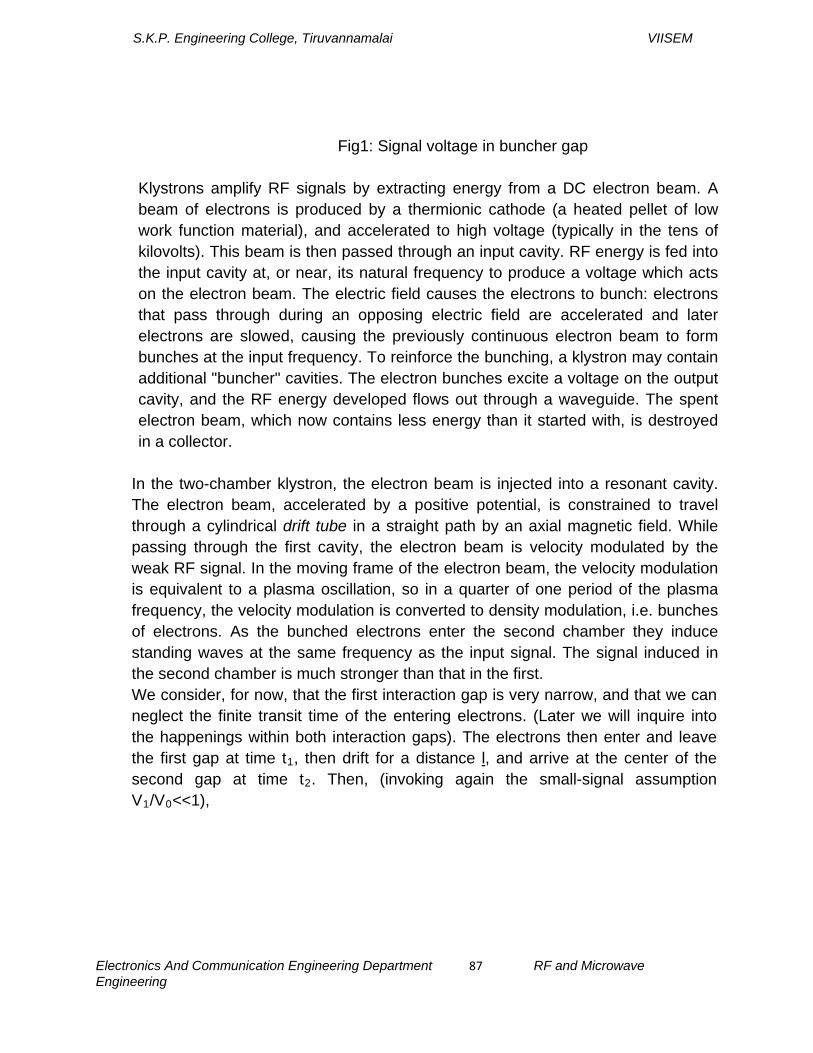
S.K.P. Engineering College, Tiruvannamalai VIISEM
Electronics And Communication Engineering Department 87 RF and Microwave Engineering
Fig1: Signal voltage in buncher gap
Klystrons amplify RF signals by extracting energy from a DC electron beam. A beam of electrons is produced by a thermionic cathode (a heated pellet of low work function material), and accelerated to high voltage (typically in the tens of kilovolts). This beam is then passed through an input cavity. RF energy is fed into the input cavity at, or near, its natural frequency to produce a voltage which acts on the electron beam. The electric field causes the electrons to bunch: electrons that pass through during an opposing electric field are accelerated and later electrons are slowed, causing the previously continuous electron beam to form bunches at the input frequency. To reinforce the bunching, a klystron may contain additional "buncher" cavities. The electron bunches excite a voltage on the output cavity, and the RF energy developed flows out through a waveguide. The spent electron beam, which now contains less energy than it started with, is destroyed in a collector.
In the two-chamber klystron, the electron beam is injected into a resonant cavity. The electron beam, accelerated by a positive potential, is constrained to travel through a cylindrical drift tube in a straight path by an axial magnetic field. While passing through the first cavity, the electron beam is velocity modulated by the weak RF signal. In the moving frame of the electron beam, the velocity modulation is equivalent to a plasma oscillation, so in a quarter of one period of the plasma frequency, the velocity modulation is converted to density modulation, i.e. bunches of electrons. As the bunched electrons enter the second chamber they induce standing waves at the same frequency as the input signal. The signal induced in the second chamber is much stronger than that in the first. We consider, for now, that the first interaction gap is very narrow, and that we can neglect the finite transit time of the entering electrons. (Later we will inquire into the happenings within both interaction gaps). The electrons then enter and leave the first gap at time t1, then drift for a distance l, and arrive at the center of the second gap at time t2. Then, (invoking again the small-signal assumption V1/V0<<1),
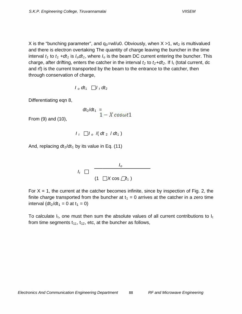
S.K.P. Engineering College, Tiruvannamalai VIISEM
Electronics And Communication Engineering Department 88 RF and Microwave Engineering
X is the “bunching parameter”, and q0=wl/u0. Obviously, when X >1, wt2 is multivalued and there is electron overtaking The quantity of charge leaving the buncher in the time interval t1 to t1 +dt1 is Iodt1, where Io is the beam DC current entering the buncher. This charge, after drifting, enters the catcher in the interval t2 to t2+dt2. If It (total current, dc and rf) is the current transported by the beam to the entrance to the catcher, then through conservation of charge,
I o dt1 I t dt2
Differentiating eqn 8,
dt2/dt1 =
From (9) and (10),
I t I o /( dt 2 / dt1 )
And, replacing dt2/dt1 by its value in Eq. (11)
It Io X cos t1 )
(1
For X = 1, the current at the catcher becomes infinite, since by inspection of Fig. 2, the finite charge transported from the buncher at t1 = 0 arrives at the catcher in a zero time interval (dt2/dt1 = 0 at t1 = 0)
To calculate It, one must then sum the absolute values of all current contributions to It from time segments t11, t12, etc, at the buncher as follows,

S.K.P. Engineering College, Tiruvannamalai VIISEM
Electronics And Communication Engineering Department 89 RF and Microwave Engineering
bn is identically equal to zero, since the integrand above is an odd function of wt1.
It turns out that the expression (15) for the an coefficients is also a representation of the Bessel functions of the first kind and nth order(Fig below)
When X<1, the series converges (17) for all values of t2. For X=1, and X>1, there are discontinuities at various t2 values as shown in Fig 3 (which would disappear if space charge were taken into account). The harmonic amplitudes correspond to the peaks of the Bessel functions (Fig. 4). Recall Figure 17 in Lecture 1 where the current It was a series of “d-functions,” and all harmonics were equal. In this case, they are almost equal. We can now calculate the output power from the fundamental (n = 1), using (16) and the maximum value of J1(X), which is 0.582 and occurs at X = 1.84. The output power is the product of the rf current I1 and the maximum voltage that can be developed across the output gap without reflecting electrons, which is the beam voltage V0. Both are peak values, so,
Pout =
Consequently, for the two-cavity klystron, without space charge and with sinusoidal voltage modulation, the maximum efficiency is 58 percent. The above derivation is completely valid, even when there is electron overtaking. The small-signal approximation used to formulate the expressions used in launching the velocity modulated beam into the drift space is not used beyond the buncher in arriving at the above result.
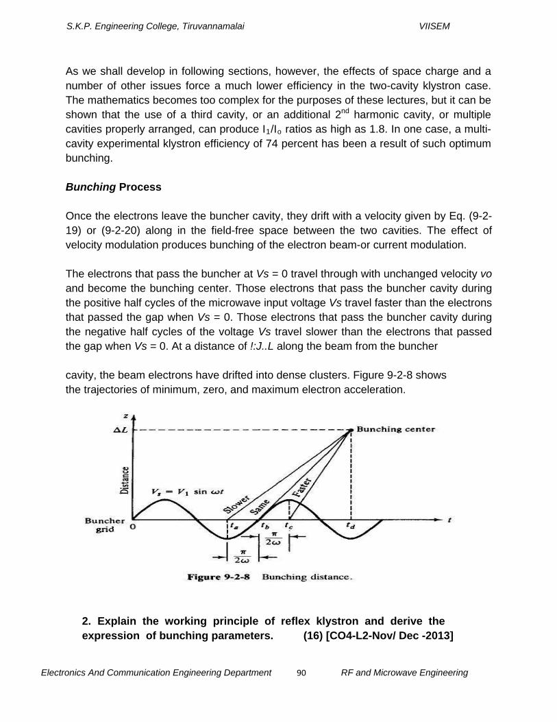
S.K.P. Engineering College, Tiruvannamalai VIISEM
Electronics And Communication Engineering Department 90 RF and Microwave Engineering
As we shall develop in following sections, however, the effects of space charge and a number of other issues force a much lower efficiency in the two-cavity klystron case. The mathematics becomes too complex for the purposes of these lectures, but it can be shown that the use of a third cavity, or an additional 2nd harmonic cavity, or multiple cavities properly arranged, can produce I1/Io ratios as high as 1.8. In one case, a multi-cavity experimental klystron efficiency of 74 percent has been a result of such optimum bunching.
Bunching Process
Once the electrons leave the buncher cavity, they drift with a velocity given by Eq. (9-2-19) or (9-2-20) along in the field-free space between the two cavities. The effect of velocity modulation produces bunching of the electron beam-or current modulation.
The electrons that pass the buncher at Vs = 0 travel through with unchanged velocity vo and become the bunching center. Those electrons that pass the buncher cavity during the positive half cycles of the microwave input voltage Vs travel faster than the electrons that passed the gap when Vs = 0. Those electrons that pass the buncher cavity during the negative half cycles of the voltage Vs travel slower than the electrons that passed the gap when Vs = 0. At a distance of !:J..L along the beam from the buncher
cavity, the beam electrons have drifted into dense clusters. Figure 9-2-8 shows the trajectories of minimum, zero, and maximum electron acceleration.
2. Explain the working principle of reflex klystron and derive the expression of bunching parameters. (16) [CO4-L2-Nov/ Dec -2013]

S.K.P. Engineering College, Tiruvannamalai VIISEM
Electronics And Communication Engineering Department 91 RF and Microwave Engineering
The reflex klystron is a single-cavity klystron that overcomes the disadvantages of the twocavity klystron oscillator. It is a low-power generator of 10 to 500-mW output at a frequency range of I to 25 GHz. The efficiency is about 20 to 30%. This type is widely used in the laboratory for microwave measurements and in microwave receivers as local oscillators in commercial, military, and airborne Doppler radars as well as missiles.
The theory of the two-cavity klystron can be applied to the nalysis of the reflex klystron with slight modification. A schematic diagram of the reflex klystron is shown in Fig. 9-4-1.
The electron beam injected from the cathode is first velocity-modulated by the cavity-gap voltage. Some electrons accelerated by the accelerating field enter therepeller space with greater velocity than those with unchanged velocity. Some electrons decelerated by the retarding field enter the repeller region with less velocity.
All electrons turned around by the repeller voltage then pass through the cavity gap in bunches that occur once per cycle. On their return journey the bunched electrons pass through the gap during the retarding phase of the alternating field and give up their kinetic energy to the electromagnetic energy of the field in the cavity. Oscillator output energy is then taken from the cavity. The electrons are finally collected by
the walls of the cavity or other grounded metal parts of the tube. Figure 9-4-2 shows an Applegate diagram for the 1~ mode of a reflex klystron.
Velocity Modulation
The analysis of a reflex klystron is similar to that of a two-cavity klystron. For simplicity, the effect of space-charge forces on the electron motion will again be neglected. The electron entering the cavity gap from the cathode at z = 0 and time to is assumed to have uniform velocity.
We begin with the equation of motion of the electron in a gridded gap field
Ez(z,t), defined as
E z ( z , t ) E m f ( z )e jt

S.K.P. Engineering College, Tiruvannamalai VIISEM
Electronics And Communication Engineering Department 92 RF and Microwave Engineering
where Em is the maximum value of the electric field in a cavity interaction gap that extends from z = 0 to z = d. The function f(z) is a “shape factor”. The maximum rf voltage across the gap is
A parameter α (for small-signal <<1) will be used to define the depth of
modulation in relation to the dc beam voltage
If the field in the gap were zero, and the electron velocity u0, the electron position after time t would be z = u0t. Since the rf modulation is small, we can write, approximately the “beam propagation factor”. The function h(z) is indeterminate for our purposes and does not enter in the calculations that follow which expressed the change in kinetic energy of an electron after going through a narrow gap, with a voltage V1 across it (time dependence omitted). V1, when modified by the coupling coefficient M, yields the “effective voltage” acting on the electrons. We now have an accurate expression for M. In a one-dimensional system it is, and, can be generalized by extending the integration over the entire z-axis. It can then be applied to 2-dimensional (gridless gap, such as that in Fig. 5, below)
more accurate, two-dimensional models. To derive a 2-dimensional expression for the coupling coefficient in ungridded cylindrical drift tubes, one must: a) assume a certain electric field at the edge of the gap at r = a, computed from the detailed nature of the drift tube tips, or determined by simulation, and calculate M at r = a, from that boundary condition, compute M as a function of r throughout the
region, andc) average the coupling coefficient over the beam.

S.K.P. Engineering College, Tiruvannamalai VIISEM
Electronics And Communication Engineering Department 93 RF and Microwave Engineering
The gap field is defined as before, this time with an r-dependence:
E z ( r , z , t ) E m f ( r , z )e jt
and at r = a,
E z ( a , z , t ) E m f ( a , z )e jt
Various authors have amused themselves over the years computing coupling coefficients for round tips, knife-edge tips, square tips, etc. Warnecke & Guenardi assume drift tubes ending in knife-edges to obtain the expression below for the field at the gap, at the drift tube radius a.Since, unlike in a closed waveguide, the axial electric field cannot be zero on axis at the center of the gap, the solution to (50) cannot be a J0, but an I0 Bessel function, which is not zero at r = 0 as J0 is. This means that z>k (or that wave the phase velocity u is lower than c and the appropriate function is I0(r)ejz,
We will now use the following identity:

S.K.P. Engineering College, Tiruvannamalai VIISEM
Electronics And Communication Engineering Department 94 RF and Microwave Engineering
The “delta function” has the property that, when multiplied by another function of β, and integrated over β from minus to plus infinity, it returns that function evaluated at βe. A klystron cavity equivalent circuit, including the beam loading conductance (and susceptance) is shown in Fig. 5 below. A value for Bb is provided in the Warnecke book. It involves some drastic approximations and usually provides a very small correction to the very cavity inductance L.
Fig –Equivalent circuit
A plot of Gb/Go is shown on Fig. 7 below. It is taken from the Warnecke & Guénard book, where the normalized parameters in terms of the usage here are: a′= b and b′= a. Note that Gb becomes negative at approximately ed/2 = 2.3 radians. The figure shows values of Gb for the beam filling the drift tube (solid lines) and for a 50% filling factor (dotted).

S.K.P. Engineering College, Tiruvannamalai VIISEM
Electronics And Communication Engineering Department 95 RF and Microwave Engineering
3. A two cavity klystron amplifier has the following parameters: Beam voltage,V0=1000v, Beam current I0=25mA:
Frequency f=3GHz,R0=40KΩ Gap spacing in either cavity,d=1mm Spacing between the two cavities,L=4cm Effective shunt impedance, Rsh=30kΩ
Calculate input gap voltage, voltage gain and efficiency. (16) [CO4-H1-Nov/Dec 12] Solution:
(a) For maximum output voltage V2, J1(X) must be maximum. This means J1(X)=0.582 at X=1.841. The electron velocity just leaving the cathode is
V0 = (0.593×10⁶) √V0
= (0.593×10⁶) √103
= (0.593×10⁶) √31.62
= 0.593x106 × 31.62 V0 = 1.88 × 10⁷m/s
(a) The d.c electron transit time across the gap,
(b) Input voltage for maximum output voltage: The gap transit
angle is
=
=
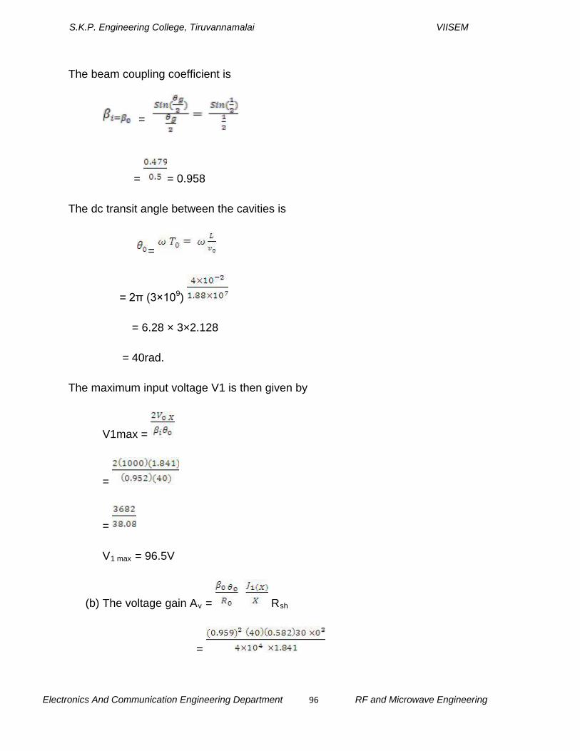
S.K.P. Engineering College, Tiruvannamalai VIISEM
Electronics And Communication Engineering Department 96 RF and Microwave Engineering
The beam coupling coefficient is
=
= = 0.958
The dc transit angle between the cavities is
=
= 2π (3×10⁹)
= 6.28 × 3×2.128
= 40rad.
The maximum input voltage V1 is then given by
V1max =
=
=
V1 max = 96.5V
(b) The voltage gain Av = Rsh
=

S.K.P. Engineering College, Tiruvannamalai VIISEM
Electronics And Communication Engineering Department 97 RF and Microwave Engineering
=
=
Av= 8.595
(a) Efficiency
η =
Where = 2 β0I0 J1(X)
I2 = 2 × 25×10 -3 ×0.582
I2 = 29.1 × 10⁻³A
V2 = β0 I2 Rsh
= (0.959) (29.1×10-
3)(30×103) V2= 831V
η =
=
η = 46.38%
5. With neat diagram, explain about Magnetron oscillator. (16) [CO4-L2-April/May-2015]
MAGNETRON OSCILLATORS
Hull invented the magnetron in 1921 [1], but it was only an interesting laboratory device until about 1940. During World War II, an urgent need for high-power microwave

S.K.P. Engineering College, Tiruvannamalai VIISEM
Electronics And Communication Engineering Department 98 RF and Microwave Engineering
generators for radar transmitters led to the rapid development of the magnetron to its present state.
All magnetrons consist of some form of anode and cathode operated in a de magnetic field normal to of the crossed field between the cathode and anode, the electrons emitted from the cathode are influenced by the crossed field to move in curved paths. If the de magnetic field is strong enough, the electrons will not arrive in the anode but return instead to the cathode. Consequently, the anode current is cut off. Magnetrons can be classified into three types:
1. Split-anode magnetron: This type of magnetron uses a static negative resistance between two anode segments.
2. Cyclotron-frequency magnetrons: This type operates under the influence of synchronism between an alternating component of electric field and a periodic oscillation of electrons in a direction parallel to the field.
3. Traveling-wave magnetrons: This type depends on the interaction of electrons with a traveling electromagnetic field of linear velocity. They are customarily referred to simply as magnetrons.
Cylindrical Magnetron
A schematic diagram of a cylindrical magnetron oscillator is shown in Fig. 10-1-1. This type of magnetron is also called a conventional magnetron.
The re-entrant feedback takes place as a result of interaction of electrons with electric field of RF oscillations existing in cavities.
Energy is transferred from the radial DC field to RF field by interaction of electron with fringing RF field.
• The oscillating RF field, makes either sides of slot alternatingly positive and negative. Due to this, electrons are retarded and attracted, leading to longest path for electrons in interaction space. When they travel long path, they transfer their energy to RF field, making them favoured electrons.
• These favoured electrons travel in a bunch, leading to bunching effect. Other electrons which spend very little time in interaction space is called as unfavoured electrons.
S.K.P. Engineering College, Tiruvannamalai VIISEM
Electronics And Communication Engineering Department 99 RF and Microwave Engineering
• Everytime an electron reached anode in phase with RF field, they complete a cycle, with a phase shift of 2π. When adjacent poles have a phase difference of π radians, it is called pi-mode.
• Magnetron should have even number of cavities, where at one instant one half of alternate ones will be positive and other alternate will be negative. In this case, the electrons are attracted and retarded, thereby transferring their energy to RF field.
• This mechanism by which electron bunches are formed and electrons are kept in synchronization with RF field, is called phase bunching effect.
• Two identical resonating cavities, will have frequencies above and below the required frequency. This happens due to mutual coupling.
• A common means of separating the pi-mode from adjacent modes by a method called strapping.

S.K.P. Engineering College, Tiruvannamalai VIISEM
Electronics And Communication Engineering Department 100 RF and Microwave Engineering

S.K.P. Engineering College, Tiruvannamalai VIISEM
Electronics And Communication Engineering Department 101 RF and Microwave Engineering
In a cylindrical magnetron, several reentrant cavities are connected to the gaps. The de voltage
Vo is applied between the cathode and the anode. The magnetic flux density Bo is in the positive z direction. When the de voltage and the magnetic flux are adjusted properly, the electrons will follow cycloidal paths. in the cathode anode space under the combined force of both electric and magnetic fields as shown in Fig. above. The equations of motion for electrons in a cylindrical magnetron can be written with the aid of Eqs.(l-2-Sa) and (1-2-Sb)
Where e/m = 1.759 x 10¹¹ C/Kg is the charge to mass ratio of the electron and its given by
r2 dɸ/dt = ½ ωc
2 r2 + constant (1)
Where ωc is the cyclotron angular frequency
At r= a, where a is the radius of cathode cylinder, the angular velocity can be expressed as
(2)
Since the magnetic fields does no work on the electrons, the kinetic energu of the electron is given by,
(3)
However the electron velocity has r and ɸ components such as,
V2 = = Vr2 + Vɸ
2 (4)
At r=b, where b is the radius from the center of the cathode to the edge of anode, V=V0 and dr/dt=0, when the electrons just graze the anode, the above equations become
(5)

S.K.P. Engineering College, Tiruvannamalai VIISEM
Electronics And Communication Engineering Department 102 RF and Microwave Engineering
(6)
The electron will acquire a tangential as well as radial velocity. Whether the electrons will just graze the anode and return toward the cathode depends on the relative magnitudes of V0 and B0. The hall cutoff magnetic condition is given as
B0= (7)
Angular frequency. Since the magnetic field is normal to the motion of electrons that travel in a cycloidal path, the outward centrifugal force is equal to the pulling force. Hence
(8)
Where,
R= radius of cylindrical path
V= tangential velocity of the electron
The cyclotron angular frequency of the circular motion of the electron is then given by
(9)
The period of one complete revolution can be expressed as
T= (10)
Since the slow-wave structure is closed on itself, or "reentrant," oscillations are possible only if the total phase shift around the structure is an integral multiple of 27T radians. Thus, if there are N reentrant cavities in the anode structure, the phase shift between two adjacent cavities can be expressed as
(11)

S.K.P. Engineering College, Tiruvannamalai VIISEM
Electronics And Communication Engineering Department 103 RF and Microwave Engineering
where n is an integer indicating the nth mode of oscillation. In order for oscillations to be produced in the structure, the anode de voltage must be adjusted so that the average rotational velocity of the electrons corresponds to the phase velocity of the field in the slow-wave structure.
Magnetron oscillators are ordinarily operated in the 7T mode. That is
Fig: Eight cavity klystron
Maxwell's equations subject to the boundary conditions. The solution for the fundamental cf> component of the electric field has the form [l]
(12)
where £ 1 is a constant and f3o is given in Eq. (10-1-18). Thus, the traveling field of the fundamental mode travels around the structure with angular velocity
(13)
where~ can be found from Eq. (10-1-19). When the cyclotron frequency of the electrons is equal to the angular frequency of the field, the interactions between the field and electron occurs and the energy is transferred. That is,
(14)
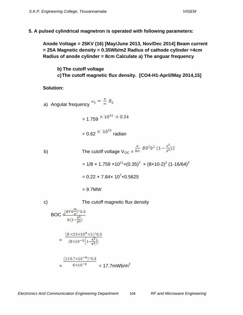
S.K.P. Engineering College, Tiruvannamalai VIISEM
Electronics And Communication Engineering Department 104 RF and Microwave Engineering
5. A pulsed cylindrical magnetron is operated with following parameters:
Anode Voltage = 25KV (16) [May/June 2013, Nov/Dec 2014] Beam current = 25A Magnetic density = 0.35Wb/m2 Radius of cathode cylinder =4cm Radius of anode cylinder = 8cm Calculate a) The anguar frequency
b) The cutoff voltage c) The cutoff magnetic flux density. [CO4-H1-April/May 2014,15]
Solution:
a) Angular frequency
= 1.759
= 0.62 radian
b) The cutoff voltage VOC =
= 1/8 × 1.759 ×1011×(0.35)2 × (8×10-2)2 (1-16/64)2
= 0.22 × 7.84× 107×0.5625
= 9.7MW
c) The cutoff magnetic flux density
BOC =
=
= = 17.7mWb/m2

S.K.P. Engineering College, Tiruvannamalai VIISEM
Electronics And Communication Engineering Department 105 RF and Microwave Engineering
6.With neat diagrams and relevant equations, explain about helix traveling wave tube. (16) [CO4-L2-April/May 2013, Nov/Dec 2014]
Since Kompfner invented the helix traveling-wave tube (TWT) in 1944 [11], its basic circuit has changed little. For broadband applications, the helix TWTs are almost exclusively used, whereas for high-average-power purposes, such as radar transmitters, the coupled-cavity TWTs are commonly used.
In previous sections klystrons and reflex klystrons were analyzed in some detail. Before starting to describe the TWT, it seems appropriate to compare the basic operating principles of both the TWT and the klystron. In the case of the TWT, the microwave circuit is nonresonant and the wave propagates with the same speed as the electrons in the beam. The initial effect on the beam is a small amount of velocity modulation caused by the weak electric fields associated with the traveling wave.
Just as in the klystron, this velocity modulation later translates to current modulation, which then induces an RF current in the circuit, causing amplification. However, there are some major differences between the TWT and the klystron:
The interaction of electron beam and RF field in the TWT is continuous over the entire length of the circuit, but the interaction in the klystron occurs only at the gaps of a few resonant cavities.
The wave in the TWT is a propagating wave; the wave in the klystron is not.
In the coupled-cavity TWT there is a coupling effect between the cavities, whereas each cavity in the klystron operates independently.
As the operating frequency is increased, both the inductance and capacitance of the resonant circuit must be decreased in order to maintain resonance at the operating frequency. Because the gain-bandwidth product is limited by the resonant circuit, the ordinary resonator cannot generate

S.K.P. Engineering College, Tiruvannamalai VIISEM
Electronics And Communication Engineering Department 106 RF and Microwave Engineering
a large output. Several nonresonant periodic circuits or slow-wave structures (see Fig. 9-5-2) are designed for producing large gain over a wide bandwidth.
Slow-wave structures are special circuits that are used in microwave tubes to reduce the wave velocity in a certain direction so that the electron beam and the signal wave can interact. The phase velocity of a wave in ordinary waveguides is greater than the velocity of light in a vacuum. In the operation of traveling-wave and magnetron-type devices, the electron beam must keep in step with the microwave signal. Since the electron beam can be accelerated only to velocities that are about a fraction of the velocity y of light, a slow-wave structure must be incorporated in the microwave devices so that the phase velocity of the microwave signal can keep pace with that of the electron beam for effective interactions. Several types of slow-wave structures are shown in figure.

S.K.P. Engineering College, Tiruvannamalai VIISEM
Electronics And Communication Engineering Department 107 RF and Microwave Engineering
Unit - V
Microwave Measurements
Part A
1. Name the possible errors VSWR measurements? [CO5-L1-Nov/Dec-12,May/june-13]
The signal source give a signal frequency. any spurious signals present leads to the shift
in maxima and minima and hence error is resulted in the readings
There should not be any undesired reflection. for this matched load can be used as shown. These undesiresd reflection cause peaks and nodes to shift position in the standing wave pattern and VSWR thus measured will not be accurate.
For higher VSWR near 10, the minimum voltage will be small and there will be deformation
in the pattern because of the high coupling at voltage maximum resulting in errors
2. What are the errors in impendence measurements [ CO5-L1-May/june-14]
a. Scalar or sensitivity errors
b. Vector errors or phase errors
3. What is the significance of VSWR measurements [CO5-L1-Nov/Dec-14]
VSWR and the magnitude of voltage reflection coefficient (Г) are very important parameters
which determine the degree of impendence matching
a. VSWR and Г are also used for measurement of load impendence by the slotted line
method
b. When a load ZL ≠ Zo is connected to transmission line, standing waves are produced

S.K.P. Engineering College, Tiruvannamalai VIISEM
Electronics And Communication Engineering Department 108 RF and Microwave Engineering
4. What is Bolometer? [CO5-L1] It is a power sensor whose resistance change with changed temperature as it absorb the microwave power. It is a short thin metallic wire sensor with positive temperature coefficient of reistance.
5. Define insertion loss? [CO5-L1]
It is defined as difference in power arriving at the terminating load .with or without The network in circuit Insertion loss(db)=10 log(po/pi)
6. What is radiation pattern? [CO5-L1] Radiation pattern is a representation of radiation characteristics of an antenna which is a function of elevation angle azimuth angle for a constant radial distance and frequency
7. What is spectrum analyzer? [CO5-L1]
Spectrum analyzer is a broad band super heterodyne receiver which is used to display a wave in frequency domain additionally, power measurements, side bands can also be observed.
8. What is the principle by which high power measurements could be done by calorimetric method? [CO5-L1-APRIL/MAY 2011]
The measurement involves conversion of microwave energy into heat, absorbing this heat in a fluid (usually water) and then measuring the temperature rice of the fluid.
9. Differentiate baretter and thermistor? [CO5-L2]
Baretter
1.baretter has positive temperature coefficient. 2.it has thin wire. 3.less sensitive. 4.required less bias current Thermistor
1.negative temp coefficient.
2.small bead of semi conductor material. 3.more sensitive.
4.require more sensitive.
10. What are tunable detector? [CO5-L1]

S.K.P. Engineering College, Tiruvannamalai VIISEM
Electronics And Communication Engineering Department 109 RF and Microwave Engineering
The tunable detectors are used to demodulate the signal and couple the
required output to high frequency scope analyzer.The low frequency demodulated output is detected using non reciprocal detector diode monunted in the microwave transmission line.
11. What is slotted section with line carriage? [CO5-L1]
It is a microwave sectioned coaxial line connecting a coaxial E-field probe which penetrates inside a rectangular waveguide slotted section.The longitudinal slot is cut along the center of the waveguide broad walls.The probe is made to move along the slotted wall which samples the electric field propotional to probe voltage.
12. What is the main purpose of slotted section with line carriage? [CO5-L2]
1.For determination of location of voltage standing wave maxima and minima along the line.
2.Measure the VSWR and standing wave pattern.
3.Wavelength.
4.Impedence.
5.Reflection coeffient.
6.Return loss measurement.
13. What is a VSWR meter? [CO5-L1]
VSWR meter is a highly sensitive,high gain,high theta,low noise voltage amplifier tuned normally at fixed frequency of 1KHZ of which microwave signals modulated.This meter indicates calibrated VSWR reading fir any loads.
14. What is calorimeter? [CO5-L1]
It is convenient device setup for measuring the high power at microwave which involves conversion of microwave energy in to heat,absorbing the heat in a f luid and determine the temp.
15. Mention the disadvantages of single bridge circuit ? [CO5-L2]

S.K.P. Engineering College, Tiruvannamalai VIISEM
Electronics And Communication Engineering Department 110 RF and Microwave Engineering
1.Change in resistance due to mismatch at the microwave input port results in incorrect reading 2The thermistor is sensitive to change in the ambient temp resulting in false Readings
16. Define insertion loss? [CO5-L1]
It is defined as difference in power arriving at the terminating load with or without the network in circuit
Insertion loss(db)=10 log(po/pi)
17. How will you determine the VSWR and return loss in reflecto meter method? [CO5-L2]
The voltage ratio between port3 or port4 is known reflecting coefficient (T) determined we determine VSWR and return loss as
VSWR=(1+T)/(1-T) Return loss=-20 log(T)
18. List the different types of Impedence measurement methods? [CO5-L2]
1.Slotted line method
2.Reflectometer method
3.Reactor discontructer method
19. How do you measure microwave frequency? [CO5-L2]
1.Wavemeter method 2.Slotted line method 3.Downconversion method 20. What is a wavemeter? [CO5-L1] It is a device used for frequency measurement in microwave.It has cylindrical cavity with a variable short circuit termination .It changes the resonant frequency of cavity by changing cavitylength.
S.K.P. Engineering College, Tiruvannamalai VIISEM
Electronics And Communication Engineering Department 111 RF and Microwave Engineering
21. Define dielectric constant? [CO5-L1]
It is defined by the ratio of permittivity of medium to permittivity of freespace. xr=x/xo=((10^-9)/36p)
22. How the S-parameter of a microwave circuit measured? [CO5-L2]
S-parameters are conveniently measured using the deschamps method which utilizes the measured value of complex input reflection coefficient under a number of a reactive terminations.
23. List the methods for measuring dielectric constants? [CO5-L2]
1.Waveguide method 2.cavity pertubaration method
24. What is radiation pattern? [CO5-L1]
Radiation pattern is a representation of radiation characteristics of an antenna which is a function of elevation angle azimuth angle for a constant radial distance and frequency.
25. What is radiation efficiency? [CO5-L1]
Radiation efficiency is defined as the ratio of total power radiated to total power accepted at its input .
26. How do you measure the polarization? [CO5-L2]
The polarization of an antenna is measured using transmitting mode and probing the polarization by a dipole antenna in the which the dipole is rotated in the plane of polarization and the received voltage pattern is recorded.
27. What is spectrum analyzer? [CO5-L1]
Spectrum analyzer is a broad band super heterodyne receiver which is used to display a wave in frequency domain additionally, power measurements, side bands can also be observed.
28. List the types of spectrum analyzer [CO5-L2]
a) Real time spectrum analyzer b) Swept tuned frequency spectrum analyzer
29. List some application of spectrum analyzer. [CO5-L2]

S.K.P. Engineering College, Tiruvannamalai VIISEM
Electronics And Communication Engineering Department 112 RF and Microwave Engineering
Identifying frequency terms and their power levels measuring harmonic distortion in a wave Determine type of wave modulation Signal to noise ratio for identifying wave distortion
30. What is network analyzer [CO5-L1]
A Network analyzer measures both amplitude and phase of a signal over a wide frequency range. It requires accurate reference signal and a test signal.
31. What is the significance of VSWR measurement? [CO5-L2-Nov/Dec2014]
VSWR and the magnitude of voltage reflection coefficient are the very important parameters which determine the degree of impedance matching.
32. Define SWR. [CO5-L1-Nov/Dec 2013]
Standing wave ratio is defined as the ratio of maximum voltage to the minimum voltage.
S= Emax/Emin
Or S= 1+Ӷ
1- Ӷ Where Ӷ= Reflection coefficient.
33. Name the errors possible in VSWR measurements. [CO5-L2-Nov/Dec 2012, May/june 2013, May/june 2014]
(i) Vmax and Vmin may not be measured in the square law region of the crystal
detector.
(ii) The probe thickness and depth of penetration may produce reflections in the line and also distortion in the field to be measured.
(iii) When VSWR is < 1.05, the associated VSWR of connector produces significant error in VSWR measurement. Very good low VSWR (<1.01) connectors should be used for very low VSWR measurements.
34. Distinguish between low frequency measurements and microwave measurements. [CO5-L2]

S.K.P. Engineering College, Tiruvannamalai VIISEM
Electronics And Communication Engineering Department 113 RF and Microwave Engineering
S.No Low frequency measuremerts Microwave measurements
1 At low frequency it is convenient to
At Microwave frequencies the
measure voltage and current and amplitude of voltage and
use them to calculate power currents on a distribution line
are the functions of a distance
and are not easily measurable.
2 At low frequency, circuits use At Microwave frequencies the
lumped elements. circuit elements are
distributed.
PART B
1. Explain the principle of microwave power measurements (8) [CO5-L2-
Nov/Dec -11, May/June 2014,April/May15]
Power Measurement
• Power is defined as the quantity of energy dissipated or stored per unit time.
• Microwave power is divided into three categories – low power (less than 10mW), medium power(from 10mW to 10W) and high power (greater than 10w). • The general measurement technique for average power is to attach a properly calibrated sensor to the transmission line port at which the unknown power is to be measured.
The output from the sensor is connected to an appropriate power meter. The RF power to the sensor is turned off and the power meter zeroed. This operation is often referred to as “zero setting” or “zeroing.” Power is then turned on.
The sensor, reacting to the new input level, sends a signal to the power meter and the new meter reading is observed.

S.K.P. Engineering College, Tiruvannamalai VIISEM
Electronics And Communication Engineering Department 114 RF and Microwave Engineering
There are three popular devices for sensing and measuring average power at RF and microwave frequencies. Each of the methods uses a different kind of device to convert the RF power to a measurable DC or low frequency signal. The devices are the diode detector, the bolometer and the thermocouple.
Diode Detector
The low-barrier Schottky (LBS) diode technology which made it possible to construct diodes with metal-semiconductor junctions for microwave frequencies that was very rugged and consistent from diode to diode. These diodes, introduced as power sensors in 1974, were able to detect and measure power as low as −70 dBm (100 pW) at frequencies up to 18 GHz.
Bolometer Sensor:
Bolometers are power sensors that operate by changing resistance due to a change in temperature. The change in temperature results from converting RF or microwave energy into heat within the bolometric element. There are two principle types of bolometers, barretters and thermistors. A barretter is a thin wire that has a positive temperature coefficient of resistance. Thermistors are semiconductors with a negative temperature coefficient.
Thermistor elements are mounted in either coaxial or waveguide structures so they are compatible with common transmission line systems used at microwave and RF frequencies.
Power meters are constructed from balanced bridge circuits. The principal parts of the power meter are two self-balancing bridges, the meter-logic section, and the auto-zero circuit. The RF Bridge, which
contains the detecting thermistor, is kept in balance by automatically varying the DC voltage Vrf, which drives that bridge. The compensating bridge, which contains the compensating thermistor, is kept in balance by automatically varying the DC voltage Vc, which drives that bridge. The power meter is initially zero-set (by pushing the zero-set button) with no applied RF power by making Vc equal to Vrfo (Vrfo means Vrf with zero RF power). After zero-setting, if ambient temperature variations change thermistor resistance, both bridge circuits respond by applying the same new voltage to maintain balance.
If RF power is applied to the detecting thermistor, Vrf decreases so that

S.K.P. Engineering College, Tiruvannamalai VIISEM
Electronics And Communication Engineering Department 115 RF and Microwave Engineering
Prf = (V2rf/4R) – (V2
rf/4R)
Where Prf is the RF power applied and R is the value of the thermistor resistance at balance. But from zero-setting, Vrfo= Vc so that
Prf = (V2
c-V2rf)/4R
Thermocouple Sensors
Thermocouple sensors have been the detection technology of choice for sensing RF and microwave power since their introduction in 1974. The two main reasons for this evolution are: 1) they exhibit higher sensitivity than previous thermistor technology, and 2) they feature inherent square-law detection characteristic (input RF power is proportional to DC voltage out).
Since thermocouples are heat-based sensors, they are true “averaging detectors.” Thermocouples are based on the fact that dissimilar metals generate a voltage due to temperature differences at a hot and a cold junction of the two metals. The power sensor contains two identical thermocouples on one chip, electrically connected as in Figure.

S.K.P. Engineering College, Tiruvannamalai VIISEM
Electronics And Communication Engineering Department 116 RF and Microwave Engineering
The thermocouples are connected in series as far as the DC voltmeter is concerned. For the RF input frequencies, the two thermocouples are in parallel, being driven through coupling capacitor Cc. Half the RF current flows through each thermocouple.
Each thin-film resistor and the silicon in series with it have a total resistance of 100 Ω. The two thermocouples in parallel form a 50 Ω termination to the RF transmission line. The lower node of the left thermocouple is directly connected to ground and the lower node of the right thermocouple is at RF ground through bypass capacitor Cb. The DC voltages generated by the separate thermocouples add in series to form a higher DC output voltage. The principal advantage, however, of the two thermocouple scheme is that both leads to the voltmeter are at RF ground; there is no need for an RF choke in the upper lead. If a choke were needed it would limit the frequency range of the sensor. For a square wave modulated signal the peak power can be calculated from the average power measured as where T is the time period and Շ is the pulse width. Y P peak av P
2. Explain how low VSWR can be measured using microwave bench (16) [CO5-L2-Nov/Dec – 2011, Nov/Dec 2012, Nov/Dec 2014]
In a microwave network, if load impedance and line impedance are not matched, signal fed from the source is reflected again towards source causing standing wave pattern in the network. Voltage Standing Wave Ratio is a measure used for finding the magnitude of ration of reflected signals maximum and minimum amplitudes For analyzing standing wave pattern and to find S slotted line carriage is used in laboratory.
Low VSWR Measurements: (S<20)

S.K.P. Engineering College, Tiruvannamalai VIISEM
Electronics And Communication Engineering Department 117 RF and Microwave Engineering
Procedure:
1.Microwave Source is energized with 1 KHz square wave signal as carrier.
2. Tunable passive components are so adjusted to get reading across the VSWR meter in 30 dB scale.
3. Detector (Tunable probe detector) is adjusted to get maximum power across the
VSWR meter.
4. Slotted line carriage is moved from the load towards source to find the standing wave minimum position.
5. By adjusting the gain control knob of VSWR meter and attenuator the reading across the VSWR meter is made as 1 or 0 dB known as normalization.
6. Again the slotted carriage is moved towards source to find the next minimum position. The reading shown at this point in the VSWR meter is the ratio of magnitude of reflected signals minimum and maximum voltages ( ). min max VV S
7. VSWR meter has three different scales with different ranges as specified below.
a) NORMAL SWR Scale 1 ---- 1 – 4
b) NORMAL SWR Scale 2 ---- 3.2 – 10
c) EXPANDED SWR Scale 3 ---- 1 – 1.33
8. If the device under test (DUT) is having the range of VSWR 1 – 4, reading is taken from the first scale from the top (NORMAL SWR Scale 1 – 1 – 4).
9. If the device under test (DUT) is having the range of VSWR 3.2 – 10, reading is taken from the second scale from the top (NORMAL SWR Scale 2 (3.2 – 10).
10. If the device under test (DUT) is having the range of VSWR 1 – 1.33, reading is taken from the third scale from the top (EXPANDED SWR Scale 3 (1 – 1.33).
11. If the device under test (DUT) is having the range of VSWR 10 – 40, a 20 dB range is selected in the VSWR meter and reading is taken from the first scale from the top (NORMAL SWR Scale 1 – 1 – 4) which is then multiplied by 10 for getting the actual reading.

S.K.P. Engineering College, Tiruvannamalai VIISEM
Electronics And Communication Engineering Department 118 RF and Microwave Engineering
Possible errors in Measurements:
1. Detector may not work square law region for both Vmax. and Vmin.
2. Depth of the probe in the slotted line carriage is made as minimum. If not, it may cause reflections in addition to the load reflections.
3. For the device having low VSWR, connector used for measurement must have proper matching with line impedance.
4. If the geometrical shape of the slotted line is not proper, Vmax. (or) Vmin. Value will not constant across the slotted line.
5.If the microwave signal is not properly modulated by a 1 KHz square wave, then signal becomes frequency modulated thereby it causes error in the Vmin. value measured. The value becomes lower than the actual.
6.Residual VSWR of slotted line carriage may cause error in the measurements.
High VSWR Measurements - Double Minima Method - (S>20)
Measurement of high VSWR needs separate procedure because the detector may not be tuned to work in square law region. An alternate method known as double minimum method is used for finding high VSWR with the same experimental set up as shown above.
Procedure:
1. Microwave Source is energized with 1 KHz square wave signal as carrier.
2. Tunable passive components are so adjusted to get reading across the VSWR
meter in 30 dB scale.
3. Detector (Tunable probe detector) is adjusted to get maximum power across the VSWR meter.
4. Slotted line carriage is moved from the load towards source to find the
standing wave minimum position. Let it be d1.
5. Slotted line carriage is moved further to find the next immediate minimum position. Let it be d2. Now g= 2(d1-d2)

S.K.P. Engineering College, Tiruvannamalai VIISEM
Electronics And Communication Engineering Department 119 RF and Microwave Engineering
6. By adjusting the gain control knob of VSWR meter and attenuator the reading
across the VSWR meter is made as 3 dB at this minimum position.
7. By taking this point as reference, slotted line carriage is moved on either side. The points at which the VSWR meter shows 0 dB reading on both sides are noted as x1 and x2.
S = λg/π(x1-x2)
8. High VSWR can be calculated by using the formula
VSWR Measurements by Return Loss (Reflectometer) Method:
To overcome the difficulties faced in slotted line carriage for measuring VSWR, reflectometer can be used. Reflectometer is a device having two directional couplers combined together with ideal coupling factor and directivity. It is a four-port device.
Experimental Procedure:
1. Microwave Source is energized with 1 KHz square wave signal as carrier.
2. Tunable passive components are so adjusted to get reading across the VSWR meter in 30 dB scale.
3. Detector (Tunable probe detector) is adjusted to get maximum power across the
VSWR meter.
4. Port 2 is with a movable short and is adjusted for getting the output across the detector to unity in VSWR meter. Port 3 is matched terminated.
5. VSWR meter and matched load at port4 and port 3 are interchanged. The
output of the port3 is noted which should be ideally equal to the output from port 4.

S.K.P. Engineering College, Tiruvannamalai VIISEM
Electronics And Communication Engineering Department 120 RF and Microwave Engineering
6. Without disturbing the VSWR meter adjustment, the unknown load is connected
at port 2 by replacing 1/гL
the short and the output at port3 is noted to obtain directly from the VSWR meter.
= - 20 log гL
Return loss = VSWR = (1+ гL)/(1- гL)
This method is well suited for loads having low VSWR. The major sources of errors are
1. Unstability of the signal source causes a change of signal power level during
measurement of input and reflected signals.
2. Non-ideal directional couplers and detectors are also sources of error.
3. Explain the procedure to measure the impedance of load. (8) [May/June-14]
The impedance at any point on a transmission line can be written in the form R+jX For comparison SWR can be calculated
S=
Where
Reflection co-efficient R=
Z0= characteristics impedance of w/g at operating frequency
Z= load impedance. The measurement is performed in following way.
The unknown device is connected to the slotted line and the position of one minima is determined. The unknown device is replaced by movable short to the slotted line . Two successive minima positions are noted.The twice of the difference between minima position will be guidewave length. One of the minima is used as reference for impedance measurement .Find the difference of reference minima and minima position obtained from unknown load. Let it be „d‟. Take a smith chart , taking „1‟ as centre,

S.K.P. Engineering College, Tiruvannamalai VIISEM
Electronics And Communication Engineering Department 121 RF and Microwave Engineering
draw a circle of radius equal to S. mark a point on circumference of smith chart towards load side at a distance equal to d/g. join the centre with this point . find the point where it cut the drawn circle.the co-ordinates of this point will show the normalized impedance of load.
PROCEDURE:
1.Setup the components and equipments as shown in figure.
2. Setup variable attenuator at minimum attenuation position.
3. Keep the control knobs of VSWR meter as
below: Range - 50db position
Input switch - Crystal low impedance Meter switch - Normal position Gain(Coarse & Fine)-Mid position
4. Keep the control knobs of Klystron power supply as below Beam voltage - „OFF‟
Mod-switch -AM Beam Voltage knob-Fully anticlockwise Reflector Voltage- Fully clockwise AM- Amplitude knob- Around fully clockwise AM- Frequency knob – Around Mid position
5. Switch „ON‟ the Klystron power supply, VSWR Meter and cooling fan switch.
6. Switch „ON‟ the beam voltage switch and set beam voltage around 250V-300V with help of beam voltage knob.
7. Adjust the reflector voltage to get some deflection in VSWR meter.
8. Maximize the deflection with AM amplitude and frequency control knob of power
supply.
9. Tune the plunger of Klystron Mount for maximum deflection.

S.K.P. Engineering College, Tiruvannamalai VIISEM
Electronics And Communication Engineering Department 122 RF and Microwave Engineering
10. Tune the reflector voltage knob for maximum deflection .
11. Tune the probe for maximum deflection in VSWR Meter.
12. Tune the frequency meter knob to get a „dip‟ on the VSWR scale and note down the frequency directly from frequency meter.
13. Keep the depth of pin S S. Tuner to around 3-4 mm and lock it.
14. Move the probe along the slotted line to get maximum deflection.
15. Adjust VSWR meter gain control knob and variable attenuator until the meter indicates 1.0 on the normal db SWR scale.
16. Move the probe to next minimum position and note down the SWR S0 on the
scale .also note down the probe position. Let it be „d‟.
17. Remove the SS tuner and matched termination and place movable short at slotted line. The plunger of short should be at zero.
Note the position of two successive minima position .let it be as d1 and d2 .Hence λg = 2(d1-d2).
1. Calculate
2. Find out the normalized impedance as described in the theory section.
3. Repeat the same experiment for other frequency if required.
4. Write a brief note on insertion loss and attenuation measurements (8) [CO5-L2]
In wireless communication systems, the transmit and receive antennas are connected to the radio through coaxial cable and/or waveguide transmission lines (Figure 1).

S.K.P. Engineering College, Tiruvannamalai VIISEM
Electronics And Communication Engineering Department 123 RF and Microwave Engineering
Insertion loss measures the energy absorbed by the transmission line in the direction of the signal path in dB/meter or
dB/feet. Transmission line losses are dependent on cable type, operating frequency and the length of the cable run. Insertion loss of a cable varies with frequency; the higher the frequency, the greater the loss. Insertion loss measurements help troubleshoot the network by verifying the cable installation and cable performance. High insertion loss in the feedline or jumpers can contribute to poor system performance and loss of coverage. Measuring insertion loss using Site Master assures accurate and repeatable.
Fig-Typical transmission system
During network deployment, maintenance, and trouble shooting phases, insertion loss can be measured by disconnecting the antenna and connecting an enclosed short at the end of the transmission line. If a Tower Mounted Amplifier (TMA) is used in the transmission feed line system, it is best to remove the TMA and antenna from the system configuration to perform an insertion loss measurement. It is best to always disconnect the cable at the same location so the measured data can be compared to the historical data for accuracy and repeatability. Using Site Master, cable insertion loss can be measured in CABLE LOSS or RETURN LOSS mode. In Cable Loss mode, Site Master automatically considers the signal traveling in both directions thus making the measurement easier for the user in the field. The following section explains the procedure to measure insertion loss in cable loss mode and return loss mode. The measurement setup and equipment required is the same for both modes Insertion Loss Measurement Setup The insertion loss measurement set up for a typical transmission feed line system is shown in Figure
2. Remove the antenna and connect an enclosed precision “short” at the end of the transmission
line. If a Tower Mounted Amplifier (TMA) is in the transmission feed line system, remove the TMA and antenna and connect an enclosed short at the end of the transmission

S.K.P. Engineering College, Tiruvannamalai VIISEM
Electronics And Communication Engineering Department 124 RF and Microwave Engineering
line. Insertion loss measurement for a transmission feed line system with a tower mounted amplifier is shown in Figure 3.
Fig- An insertion loss measurement setup after the antenna is removed
Fig-An insertion loss measurements setup when TMA is in line
Procedure Step
Step 1. Power On the Site Master and press the MODE key.
Step 2. Select FREQ-CABLE LOSS using the Up/Down arrow key and press ENTER.
Step 3. Set the start and stop frequencies F1 and F2. As an example, F1=750 MHz and F2=850 MHz for a typical cellular frequency band.
Step 4. Connect the phase stable test port extension cable to the RF port.
Step 5. Calibrate the Site Master at the end of the phase stable test port extension cable. (See the section entitled “Calibrating Site Master with the Phase Stable Test Port Extension Cable” for details.)

S.K.P. Engineering College, Tiruvannamalai VIISEM
Electronics And Communication Engineering Department 125 RF and Microwave Engineering
Step 6. Disconnect the antenna and connect an enclosed precision "short" at the end of the transmission line.
Step 7. Connect the other end of the transmission line to the phase stable cable of the Site Master. A trace will be displayed on the screen when the Site Master is in continuous sweep mode.
Step 8. Press the AMPLITUDE key and set the TOP and BOTTOM values of the display. In Figure 4, the TOP is set to 2 dB, and the BOTTOM is set to 5 dB.
Step 9. Press the MARKER key.
Step 10.Set M1 to MARKER TO PEAK. Step 11.Set M2 to MARKER TO VALLEY.
Step 12.Calculate the insertion loss by averaging M1 (MARKER TO PEAK) and M2 (MARKER TO VALLEY) values as follows:
Step 13. Press SAVE DISPLAY and name the trace using the soft keys and Press ENTER.
5. Explain spectrum analyzer and its uses.(16) [CO5-L2-Aril/May 2014]
A spectrum analyzer or spectral analyzer or signal analyzer is a device used to examine the spectral composition of some electrical, acoustic, or optical waveforms. It also measures the power spectrum. A spectrum analyzer displays signal amplitude (strength) as it varies by signal frequency. The frequency appears on the horizontal axis, and the amplitude is displayed on the vertical axis. To the casual observer, a spectrum analyzer looks like an oscilloscope and, in fact, some lab instruments can function either as an oscilloscope or a spectrum analyzer. A spectrum analyzer is used to determine whether a wireless transmitter is working according to federally-defined standards for purity of emissions. Output signals at frequencies other than the intended communications frequency appear as vertical lines (pips) on the display. A spectrum analyzer is also used to determine, by direct observation, the bandwidth of a digital or analog signal. A spectrum analyzer interface is a device that connects to a wireless receiver or a personal computer to allow visual detection and analysis of electromagnetic signals over a defined band of frequencies. This is called panoramic

S.K.P. Engineering College, Tiruvannamalai VIISEM
Electronics And Communication Engineering Department 126 RF and Microwave Engineering
reception and it is used to determine the frequencies of sources of interference to wireless networking equipment, such as Wi-Fi and wireless routers.
Types
There are analog and digital spectrum analyzers: An analog spectrum analyzer
uses either a variable band-pass filter or a superheterodyne receiver. With a band-pass filter, the mid-frequency is automatically tuned (shifted, swept) through the range of frequencies of which the spectrum is to be measured. With a superheterodyne receiver, the local oscillator is swept through a range of frequencies.
A digital spectrum analyzer computes the discrete Fourier transform (DFT), a
mathematical process that transforms a waveform into the components of its frequency spectrum. Some spectrum analyzers (such as "real-time spectrum analyzers") use a hybrid technique where the incoming signal is first down-converted to a lower frequency using superheterodyne techniques and then analyzed using fast fourier transformation (FFT) techniques.
Form Factor
Spectrum analyzers tend to fall into two form factors: bench top and
handheld. Bench top
This form factor is useful for applications where the spectrum analyzer can be plugged into AC power, which generally means in a lab environment or production/manufacturing area. Bench top spectrum analyzers have historically offered better performance and specifications than the handheld form factor. Bench top spectrum analyzers normally have multiple fans (with associated vents) to dissipate heat produced by the processor. Due to their architecture, bench top spectrum analyzers typically weigh more than 30 pounds (14 kg). Some bench top spectrum analyzers offer optional battery packs, allowing them to be used away from AC power. This type of analyzer is often referred to as a "portable" spectrum analyzer.
Handheld

S.K.P. Engineering College, Tiruvannamalai VIISEM
Electronics And Communication Engineering Department 127 RF and Microwave Engineering
This form factor is useful for any applications where the spectrum analyzer needs to be taken outside to make measurements or simply carried while in use. Attributes that contribute to a useful handheld spectrum analyzer include:
Battery-powered operation (and the ability to swap the battery while in the field)
to allow the user to move freely outside.
No fans and no vents, to prevent the ingress of environment contaminants.
Clearly-viewable display to allow the screen to be read in bright sunlight, darkness or dusty conditions.
Light weight (usually less than 15 pounds (6.8 kg) and preferably less than 10
pounds
(4.5 kg)) to enable easy carrying, whether on level surfaces, or while climbing up antennas or down into maintenance areas.
Frequency range
Two key spectrum analyzer parameters are frequency and span. Frequency specifies the center of the display. Span specifies the range between the start and stop frequencies, also referred to as the bandwidth of the analysis. Sometimes it is possible to specify the start and stop frequency rather than center and range.
Marker/peak search
Controls the position and function of markers and indicates the value of power. Several spectrum analyzers have a "marker delta" function that is used to measure the signal-to-noise ratio or bandwidth. Bandwidth/average
It is a filter of resolution. The spectrum analyzer captures the measure on having displaced a filter of small bandwidth along the window of frequencies.
Amplitude

S.K.P. Engineering College, Tiruvannamalai VIISEM
Electronics And Communication Engineering Department 128 RF and Microwave Engineering
The maximum value of a signal at a point is called amplitude. A spectrum analyzer that implements amplitude analysis is called a Pulse height analyzer.
View/trace
It Manages parameters of measurement. It stores the maximum values in each frequency and a solved measurement to compare it.
Usually, a spectrum analyzer displays a power spectrum over a given frequency range, changing the display as the properties of the signal change. There is a trade-off between how quickly the display can be updated and the frequency resolution, which is for example relevant for distinguishing frequency components that are close together. With a digital spectrum analyzer, the frequency resolution is Δν = 1 / T, the inverse of the time T over which the waveform is measured and Fourier transformed (according to uncertainty principle). With an analog spectrum analyzer, it is dependent on the bandwidth setting of the bandpass filter. However, an analog spectrum analyzer will not produce meaningful results if the filter bandwidth (in Hz) is smaller than the square root of the sweep speed (in Hz/s)[citation needed] , which means that a digital analyzer will always outperform an analog device in terms of frequency resolution for a given acquisition time. Choosing a wider bandpass filter will improve the signalto-noise ratio at the expense of a decreased frequency resolution.
With Fourier transform analysis in a digital spectrum analyzer, it is necessary to sample the input signal with a sampling frequency νs that is at least twice the bandwidth of the signal, due to the Nyquist limit[1]. A Fourier transform will then produce a spectrum containing all frequencies from zero to νs / 2. This can place considerable demands on the required analog- todigital converter and processing power for the Fourier transform. Often one is only interested in a narrow frequency range, for example between 88 and 108 MHz, which would require at least a sampling g frequency of 216 MHz, not counting the low-pass anti-aliasing filter. In such cases, it can be more economical to first use a superheterodyne receiver to transform the signal to a lower range, such as 8 to 28 MHz, and then sample the signal at 56 MHz. This is how an analog-digital-hybrid spectrum analyzer works. For very weak signals, a pre-amplifier is used, although harmonic and intermodulation distortion may lead to the creation of new frequency components that were not present in the original signal. A new method, which doesn't use a high local oscillator (LO) (that usually produces a high-frequency signal close to the signal) is used on the latest analyzer generation

S.K.P. Engineering College, Tiruvannamalai VIISEM
Electronics And Communication Engineering Department 129 RF and Microwave Engineering
like Aaronia´s Spectran series. The advantage of this new method is a very low noise floor near the physical thermal noise limit of -174 dBm (1Hz).
6. With experimental setup explain in detail about the
impedance measurements. (16) [CO5-L2-Nov/Dec 2013]
Impedance Measurements Using a Slotted Line
Slotted-line measurement techniques are simple and accurate methods for measuring impedance, VSWR, and reflection coefficients at microwave frequencies. The measurement apparatus consists of an air-dielectric transmission line with a small probe that can be slid along the length of the transmission line to pick off a small amount of the signal (electric field), thus giving an indication of the RF voltage as a function of position along the line. In order to achieve the best possible sensitivity and noise immunity with slotted-line measurements, the microwave source should be modulated (AM), and a narrow-band AC measurement made. This is most conveniently done using an HP 415 SWR meter, which is essentially a calibrated log-scale ac voltmeter. The modulation frequency for the source should match the center frequency of the particular SWR meter being used – typical values are in the vicinity of 1 kHz, and the exact value is labeled on the front of each meter. The SWR meter should be connected to the detector of the slotted line (replacing the DMM), and at each measurement frequency the stub tuner should be adjusted to maximize the received signal. A detailed example outlining the measurement procedure for finding impedances using the slotted line is provided in Example 2.4 (page 71-73) in Pozar, which is included at the end of this lab handout. Please read through this example problem and be familiar with it before performing the slotted-line portion of the lab.
a.) Measure a short (type N female) at 1 GHz. Find more than one minimum along the line; calculate the distance between minima (λ/2); since the dielectric in the slotted line is air, the propagation velocity of the electromagnetic wave is the speed of light; use this fact to calculate the frequency and compare to the set frequency of the microwave source.
b.) Measure an open at 1 GHz. Again find more than one minimum and calculate the frequency obtained. Compare the locations of the minima obtained for the open and short-terminated lines. c.) Measure the VSWR and the impedance of the 100 Ω GR termination at 1 GHz.
d)Measure the impedance of the microstrip stub circuit (terminate the second port with a 50 Ω type N termination) at frequencies of 500 MHz, 1000 MHz, 1500 MHz, and 2500

S.K.P. Engineering College, Tiruvannamalai VIISEM
Electronics And Communication Engineering Department 130 RF and Microwave Engineering
MHz. Note that in order to do this you will need to find the location of a null for a short at each frequency, as well as adjust the stub tuner for best response at each frequency. Plot the results on a smith chart and note which of the microstrip stub circuits you are measuring; in a future lab you will compare the measurements made with the slotted line to those obtained using other techniques.
7. Explain in detail on the measurement of scattering parameters. (8)
[CO5-L2-Nov/Dec 2015] The vector voltmeter measures the magnitude of a reference and test voltage and the difference in phase between the voltages. Because it can measure phase, it allows us to directly measure the S-parameters of a circuit. Unfortunately, the use of directional couplers and test cables connecting the measuring system to the vector voltmeter introduces unknown attenuation and phase shift into the measurements. These can be compensated for by making additional "calibration" measurements. A) Reflection measurements: obtain S11 or S22 Set up the experimental arrangement shown in Figure 1. It is seen that the voltage at channel A of the vector voltmeter ( ) D A is proportional to the amplitude of the voltage wave entering the device under test (DUT) ( ) D 1 a . Similarly, the voltage at channel B ( ) D B is proportional to the amplitude of the voltage wave reflected from the DUT ( ) D 1 b . Thus, we can write
where KA and KB are constants that depend on the connecting cables. Since a D 2 is zero because of the matched load at port 2, S11 is given by
S11 = =
To find KA and KB it is necessary to make a second measurement with a known DUT. This is called a "calibration" measurement. If the DUT in Figure 1 is removed and replaced by a short circuit, the voltages at channel A ( ) S A and channel B ( ) S B are given by
AS = KA a1
S BS

S.K.P. Engineering College, Tiruvannamalai VIISEM
Electronics And Communication Engineering Department 131 RF and Microwave Engineering
where a S 1 is the amplitude of the voltage wave entering the short and b S 1 is the amplitude of the voltage wave reflected from the short. However, for a short circuit the ratio of these amplitudes is -1 (reflection coefficient of a short). Thus
Thus
Finally, substituting this into S11 equation
S11 = -
Note that since the vector voltmeter displays quantities in terms of magnitude and phase, (6) can be written more conveniently as
S11 =
Where

S.K.P. Engineering College, Tiruvannamalai VIISEM
Electronics And Communication Engineering Department 132 RF and Microwave Engineering