slac-pub-95-7070 qs/o7!--y the vertex detector upgrade based …/67531/metadc626204/m2/1/high... ·...
TRANSCRIPT

SLAC-PUB-95-7070 December 1995
VXD3: the SLD Vertex Detector Upgrade Based on a 307 MPixel CCD System WNfv QS/O7!--y
James E. Brau University of Oregon, Eugene, OR
representing the SLD Collaboration** Stanford Linear Accelerator Center
Stanford University, CA 94309
Abstract The SLD upgrade CCD vertex detector (VXD3) is
described. Its 307 million pixels are assembled from 96 3.2 Mpixel CCDs of 13 cm2 each. The system has evolved from the pioneering CCD vertex detector VXD2, which has operated in SLD since 1992. The CCDs of VXD3 are mounted on beryllium ladders in three cylinders, providing three space point measurements along each track of about 5 microns resolution in all three co-ordinates. Significant improvements are achieved with VXD3 in impact parameter resolution (about a factor of two) and acceptance (-20%) through optimized geometry and reduced material. New readout electronics have been developed for this system.
I. INTRODUCTION
The SLD Collaboration is building a new vertex detector (VXD3) based on 96 CCDs of 13 cm2 area each, for a total of 307,000,000 pixels. This system will significantly advance the performance of the SLD vertex reconstruction from its already world class status. The original SLD pixel vertex detector VXD2 l , placed close to the e+e- intersection point(IP), in conjunction with small SLC beam spots, has provided SLD with excellent flavor-tagging for three years. The successful
operation of this 120 MPixel device is a validation of its suitability for the special SLC beam environment. The experience with VXD2 has answered the fundamental questions about the mechanical stability, hit efficiency, and resolution capability associated with a CCD-based pixel vertex detector. VXD2 has the worlds best capability in many performance criteria. Nevertheless, due to the limitations of technology at the time of designing VXD2, limited resources, stringent time schedule, and some conservatism necessarily attached to a pioneering design, some aspects of the performance were compromised. The upgrade to VXD3 (illustrated in figure 1) will significantly improve performance and open new, exciting possibilities for physics at SLD.
This work was supported by Department of Energy contracts: DE-FG03-93ER40788 (CSU), DE-FGOZ 92ER40715 (Massachusetts), DE-AC02-
(Oregon), DE-AC03-76SF00515 (SLAC), DE- AC02-76ER00881 (Wisconsin), DE-FGO2- 92M40704 (Yale); National Science Foundation grant PHY-92-03212 (Washington); the UK Science and Engineering Research Council (Brunel and RAL); the Istituto Nazionale di Fisica Nucleare of Italy (Bologna, Ferrara, Frascati, Pisa, Padova, Perugia); and the'Japan-US Cooperative Research Project on High Energy Physics (Nagoya, Tohoku).
76ER03069 (MIT), DE-FG06-85ER40224
Figure 1. Illustration of VXD3.
Presented at the Nuclear Science Symposium (NNS), San October 21-28, 1995
QISTR~BUTJON OF mi§ DOCUMENT Is U N L f M m q
Advances in the technology of CCD detectors have made it possible to design a vertex detector with much better impact parameter resolution, larger solid angle coverage and virtually error-free track linking. These will allow a world-class measu remen t of t he polarization-enhanced forward- backward asymmetry for b- and c- quarks and improved precision in the measurement of the b-fraction in hadronic Z decays, sufficient for testing radiative corrections in electroweak theory. A wide range of measurements can be made which will make use of full separation of primary, secondary and tertiary vertices. The most exciting new possibility, afforded by the upgrade, however, is the search for Bs-mixing - leading to a measurement of the mixing
X-Y Impact Parameter 250
200
n rA
150 k 0
3 v
g 100
2
.- 4 5 ' 50
d
0 10 -I 10 (I 10 10
Momentum (GeV/c)
R-Z Impact Parameter 250
200
n m 8 150 k 0
2 W
3 100 3
8 50 p:
3 .-.I
0 10 10 10 10
Momentum (GeV/c)
2
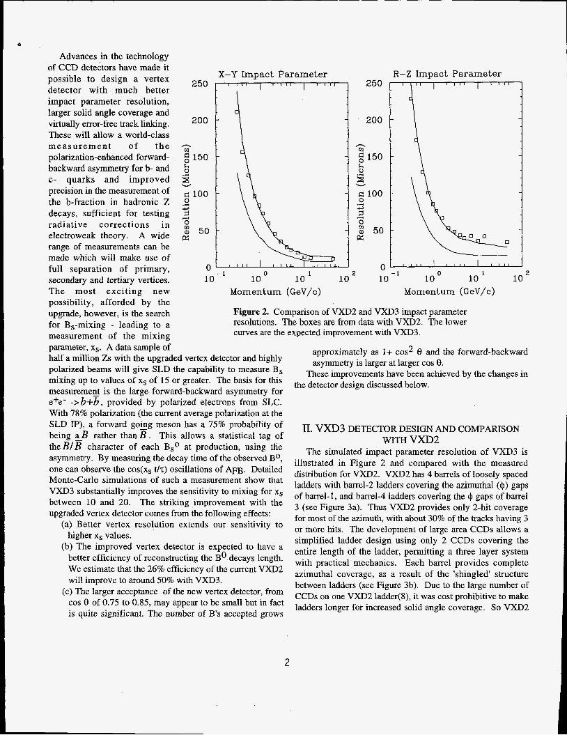
Figure 2. Comparison of VXD2 and VXD3 impact parameter resolutions. The boxes are from data with VXD2. The lower curves are the expected improvement with VXD3.
parameter, xs. A data sample of half a million Zs with the upgraded vertex detector and highly polarized beams will give SLD the capability to measure Bs mixing up to values of xs of 15 or greater. The basis for this measureme@ is the large forward-backward asymmetry for e+e- -> b+b , provided by polarized electrons from SLC. With 78% polarization (the current average polarization at the SLD IP), a forward going meson has a 75% probability of being a B rather than B. This allows a statistical tag of t heB/B character of each Bso at production, using the asymmetry. By measuring the decay time of the observed Bo, one can observe the cos(xs t/z) oscillations of AFB. Detailed Monte-Carlo simulations of such a measurement show that VXD3 substantially improves the sensitivity to mixing for xs between 10 and 20. The striking improvement with the upgraded vertex detector comes from the following effects:
(a) Better vertex resolution extends our sensitivity to higher xs values.
(b) The improved vertex detector is expected to have a better efficiency of reconstructing the Bo decays length. We estimate that the 26% efficiency of the current VXD2 will improve to around 50% with VXD3.
(c) The larger acceptance of the new vertex detector, from cos 8 of 0.75 to 0.85, may appear to be small but in fact is quite significant. The number of B's accepted grows
approximately as I+ cos2 8 and the forward-backward asymmetry is larger at larger cos 8.
These improvements have been achieved by the changes in the detector design discussed below.
u. VXD3 DETECTOR DESIGN AND COMPARISON WITH vxD2
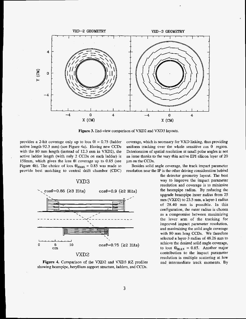
The simulated impact parameter resolution of VXD3 is illustrated in Figure 2 and compared with the measured distribution for VXD2. VXD2 has 4 barrels of loosely spaced ladders with barrel-2 ladders covering the azimuthal ($) gaps of barrel- 1, and barrel-4 ladders covering the + gaps of barrel 3 (see Figure 3a). Thus VXD2 provides only 2-hit coverage for most of the azimuth, with about 30% of the tracks having 3 or more hits. The development of large area CCDs allows a simplified ladder design using only 2 CCDs covering the entire length of the ladder, permitting a three layer system with practical mechanics. Each barrel provides complete azimuthal coverage, as a result of the 'shingled structure between ladders (see Figure 3b). Due to the large number of CCDs on one VXD2 ladder@), it was cost prohibitive to make ladders longer for increased solid angle coverage. So VXD2
2
n
G W
VXD-2 GEOMETRY VXD-3 GEOMETRY I , , I , I , I , ,
4 -
0 -
-4 -
I , I , I , t , I , I , I l l 1 -4 0 4 -4 0 4
Figure 3. End-view comparison of VXD2 and VXD3 layouts.
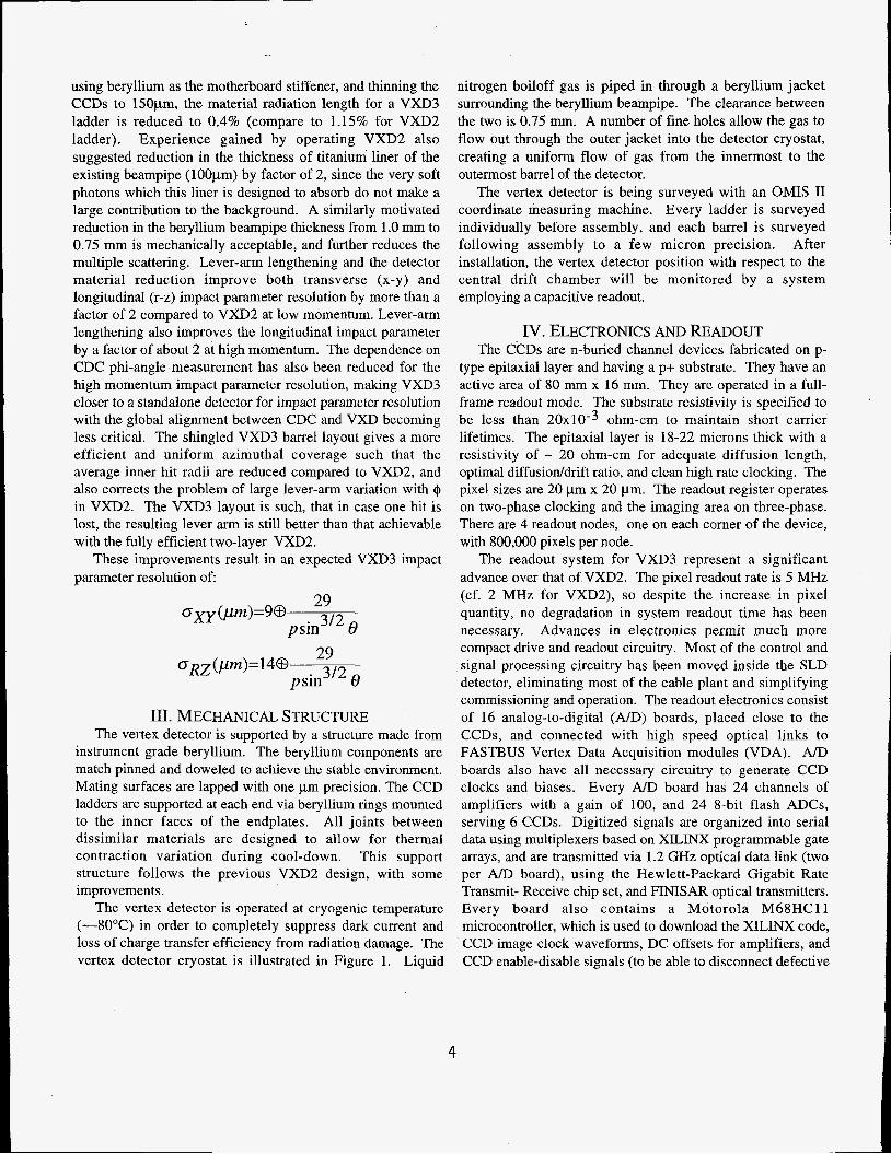
provides a 2-hit coverage only up to lcos 81 = 0.75 (ladder active length 92.3 mm) (see Figure 4a). Having new CCDs with the 80 mm length (instead of 12.3 mm in VXD2), the active ladder length (with only 2 CCDs on each ladder) is 158mm, which gives the lcos 81 coverage up to 0.85 (see Figure 4b). The choice of lcos 81max = 0.85 was made to provide best matching to central drift chamber (CDC)
coverage, which is necessary for VXD linking, thus providing uniform tracking over the whole sensitive cos 8 region. Deterioration of spatial resolution at small polar angles is not an issue thanks to the very thin active EPI silicon layer of 20 pm on the CCDs.
Besides solid angle coverage, the track impact parameter resolution near the IP is the other driving consideration behind
the detector geometry layout. The best
cosO=O.9 (22 Hits)
VXD3 .', cosB=O.85 (23 Hits)
cosO=O.75 (82 Hits)
VXD2
way to improve the impact parameter resolution and coverage is to minimize the beampipe radius. By reducing the upgrade beampipe inner radius from 25 mm (VXD2) to 23.5 mm, a layer-1 radius of 28.40 mm is possible. In this configuration, the outer radius is chosen as a compromise between maximizing the lever arm of the tracking for improved impact parameter resolution, and maximizing the solid angle coverage with 80 mm long CCDs. We therefore selected a layer-3 radius of 48.26 mm to achieve the desired solid angle coverage, to lcos elmax = 0.85. Another major contribution to the impact parameter resolution is multiple scattering at low and intermediate track momenta. By Figure 4. Comparison of the VXD2 and VXD3 RZ profiles
showing beampipe, beryllium support structure, ladders, and CCDs.
3
using beryllium as the motherboard stiffener, and thinning the CCDs to 15Opm, the material radiation length for a VXD3 ladder is reduced to 0.4% (compare to 1.15% for VXD2 ladder). Experience gained by operating VXD2 also suggested reduction in the thickness of titanium liner of the existing beampipe (1OOpm) by factor of 2, since the very soft photons which this liner is designed to absorb do not make a large contribution to the background. A similarly motivated reduction in the beryllium beampipe thickness from 1 .O mm to 0.75 mm is mechanically acceptable, and further reduces the multiple scattering. Lever-arm lengthening and the detector material reduction improve both transverse (x-y) and longitudinal (r-z) impact parameter resolution by more than a factor of 2 compared to VXD2 at low momentum. Lever-arm lengthening also improves the longitudinal impact parameter by a factor of about 2 at high momentum. The dependence on CDC phi-angle measurement has also been reduced for the high momentum impact parameter resolution, making VXD3 closer to a standalone detector for impact parameter resolution with the global alignment between CDC and VXD becoming less critical. The shingled VXD3 barrel layout gives a more efficient and uniform azimuthal coverage such that the average inner hit radii are reduced compared to VXD2, and also corrects the problem of large lever-arm variation with + in VXD2. The VXD3 layout is such, that in case one hit is lost, the resulting lever arm is still better than that achievable with the fully efficient two-layer VXD2.
These improvements result in an expected VXD3 impact parameter resolution of:
111. MECHANICAL STRUCTURE The vertex detector is supported by a structure made from
instrument grade beryllium. The beryllium components are match pinned and doweled to achieve the stable environment. Mating surfaces are lapped with one pm precision. The CCD ladders are supported at each end via beryllium rings mounted to the inner faces of the endplates. All joints between dissimilar materials are designed to allow for thermal contraction variation during cool-down. This support structure follows the previous VXD2 design, with some improvements.
The vertex detector is operated at cryogenic temperature (--80°C) in order to completely suppress dark current and loss of charge transfer efficiency from radiation damage. The vertex detector cryostat is illustrated in Figure 1. Liquid
nitrogen boiloff gas is piped in through a beryllium jacket surrounding the beryllium beampipe. The clearance between the two is 0.75 mm. A number of fine holes allow the gas to flow out through the outer jacket into the detector cryostat, creating a uniform flow of gas from the innermost to the outermost barrel of the detector.
The vertex detector is being surveyed with an OMIS I1 coordinate measuring machine. Every ladder is surveyed individually before assembly, and each barrel is surveyed following assembly to a few micron precision. After installation, the vertex detector position with respect to the central drift chamber will be monitored by a system employing a capacitive readout.
Iv. ELECTRONICS AND READOUT The CCDs are n-buried channel devices fabricated on p-
type epitaxial layer and having a p+ substrate. They have an active area of 80 mm x 16 mm. They are operated in a full- frame readout mode. The substrate resistivity is specified to be less than ~ O X ~ O - ~ ohm-cm to maintain short carrier lifetimes. The epitaxial layer is 18-22 microns thick with a resistivity of - 20 ohm-cm for adequate diffusion length, optimal diffusioddrift ratio, and clean high rate clocking. The pixel sizes are 20 pm x 20 pm. The readout register operates on two-phase clocking and the imaging area on three-phase. There are 4 readout nodes, one on each corner of the device, with 800,000 pixels per node.
The readout system for VXD3 represent a significant advance over that of VXD2. The pixel readout rate is 5 MHz (cf. 2 MHz for VXD2), so despite the increase in pixel quantity, no degradation in system readout time has been necessary. Advances in electronics permit much more compact drive and readout circuitry. Most of the control and signal processing circuitry has been moved inside the SLD detector, eliminating most of the cable plant and simplifying commissioning and operation. The readout electronics consist of 16 analog-to-digital (A/D) boards, placed close to the CCDs, and connected with high speed optical links to FASTBUS Vertex Data Acquisition modules (VDA). A/D boards also have all necessary circuitry to generate CCD clocks and biases. Every A/D board has 24 channels of amplifiers with a gain of 100, and 24 8-bit flash ADCs, serving 6 CCDs. Digitized signals are organized into serial data using multiplexers based on XILINX programmable gate arrays, and are transmitted via 1.2 GHz optical data link (two per A/D board), using the Hewlett-Packard Gigabit Rate Transmit- Receive chip set, and FINISAR optical transmitters. Every board also contains a Motorola M68HCll microcontroller, which is used to download the XILINX code, CCD image clock waveforms, DC offsets for amplifiers, and CCD enable-disable signals (to be able to disconnect defective
4
CCDs from bias and clock sources). There is also a possibility to put the board into calibration mode, when pulses of known amplitudes are generated and connected to the CCD output nodes. The microcontroller is functional only during initial (after power on) download phase of operation, or on demand to change any settings. During readout of data, the microcontroller clocks are off, to reduce the possibility of noise increase due to crosstalk to amplifier inputs. During readout all functionality of the A/D board is provided by the fast logic sequencer, a device based on the AMD fast programmable logic MACH220 chip. VDA modules are a modification of those used in VXD2. The main function of the VDA module is to reduce the 307 Mbytes of raw data to a manageable size (< 100 kbytes). This is achieved by hardware reconstructing 2-d clusters of charge deposition and imposing a threshold that gives > 99% efficiency for minimum ionizing particles traversing 20pm of silicon. Modification of the VDA boards involves usage of the faster processor (MC68040 instead of MC68020), larger front end and processor memory, new cluster processor design, and new front end design.
V. CCD PERFORMANCE RESULTS Because of the unique requirements of the CCDs for
VXD3, it was essential to have prototype devices fabricated and tested before production of the full batch of devices. The CCD manufacturering:! proceeded in two phases: the first phase for design and production of a few CCDs. The phase 1 CCDs were first tested at low temperature at SLAC, where they were methodically evaluated to verify that all specifications were met. After positive results of this test, phase 2 production of the bulk of the CCDs was started. The first phase CCDs were manufactured with two designs of output node amplifiers (actually 2-stage source followers). The first stage employed either a surface channel or a buried channel FET. The advantage of the buried channel FET is its lower noise level. But this type of device requires a higher power supply voltage and, consequently, higher power dissipation on the CCD, which is not desirable due to the limited cooling system resources. In the February, 1995, we received phase 1 devices, and tested them for noise, responsivity, charge transfer efficiency, spurious charge generation, and charge trapping. Following their evaluation, phase 2 started in April, 1995.
The noise level for the phase 1 CCDs with a buried channel FET in the output node was about 27 electron charges rms. For the surface channel FET in the first stage output node, the noise level is about 45 e, which is also within specification. The optimum power supply voltage for buried channel - surface channel options are 22 V and 17 V respectively. Because of the power dissipation concerns, and because the surface channel option satisfies the specified noise
level, it was decided to choose this type of devices for production.
The detector responsivity was measured using signals from an Fe55 radioactive source. Its value of 3.1 pV/e, combined with the gain of 100 the on A D boards and the minimum ionizing particle production of 1200 electron-hole pairs in the detector sensitive layer (20 micron), produces a signal of about 360 mV on the ADC input, or about 45 ADC counts.
The charge transfer efficiency was measured both for transfer along the R register, and through the image area, from the degradation in the cluster central pixel signal amplitude. The inefficiency per pixel was less than 5 ~ 1 0 - ~ in the R register and less than l ~ l O - ~ along the image area.
Due to defects in silicon or in manufacturing, there is a possibility of abnormal high charge accumulation in certain pixels during the detector integration time. We call such pixels "hot", and a maximum number of such hot pixels was included in the specifications. Most of the phase 1 CCDs had very few hot pixels (typically none, sometimes 1 or 2 per CCD). Another source of spurious charge generation was found in some CCDs, which generated current, leaking into the R register. Though the generated charge usually also was within specification, the manufacturer claims that they know the source of this charge (spurious tunnel diode structure, introduced as a result of a design error in the gate protection circuit), and will eliminate this in the production phase.
The phase 1 CCDs suffered from a number of "charge trap" sites. The smallest irregularities in the electric field in the silicon may create potential pockets, which may retain some of the charge as it moves through. Because such defects may be randomly distributed across the CCD area, the probability for charge moving along the area to encounter such a "charge trap" is proportional to the length of the path the charge has to travel, and so it affects large area CCDs more than small devices. We devoted a large effort to investigating the nature of these traps, and their effect on detector efficiency. Some of them absorb such a large amount of charge that the entire signal from a minimum ionizing particle is lost. Others just reduce the signal amplitude, so the signal still may be used to find the particle coordinate, but the precision of such measurement may suffer. Typical phase 1 CCDs had 1-2 completely blocked columns per node (out of 400) due to such traps; since the part of the blocked column between the location of the trap and the R register does not suffer, it leads to a 0.125 - 0.25% inefficiency. Also about 3-5 columns with smaller charge loss usually were seen in every channel.
Though such inefficiency is quite acceptable, some modifications of the CCD design were made for phase 2 to reduce the number of these charge traps. The manufacturer believed that mask misalignments were the major cause of
5
these traps. Overlapping of I-clock strips was minimized in the design to reduce the capacitance, and misalignment can produce gaps between I-clocks phases. These gaps may create traps due to charge accumulation in the silicon oxide passivation below the polysilicon I-clock strips. The overlap was increased slightly for phase 2 Also, the supplementary channel, which was included in phase 1 to increase the radiation hardness of the CCD, was removed in phase 2, since it also could contribute to the observed trapping. From tests we determined that the radiation hardness of the detectors is much better than needed, and the supplementary channels are unnecessary.
One of the phase 1 CCDs was exposed to the radiation from a Co60 source with the total accumulated dose of 15 kRad. We measured the detector parameters a few times during the exposure and did not find any serious degradation in the detector performance. With the full dose, a small (-10%) loss of signal amplitude from the Fe55 source was observed.
The first 82 production (phase 2) CCDs were delivered and tested at SLAC by early November, 1995. The performance of 74 of these were acceptable based on tests at SLAC. Eight of them were returned to the factory for replacement.
VI. CONCLUSION The SLD Collaboration is constructing an upgrade vertex
detector which will open new opportunities for heavy quark physics at the SLD. This detector is scheduled to begin data collection with the SLD experiment early in 1996, and continue for at least three years of operation.
** The SLD Collaborators working on the VXD3 upgrade are: N. Allen, P. Dervan, A. McKemey, S. Watts (Brunel Univ.), J. Harton, M. Smy (Colo. State U.), S. Hertzbach, R. Kofler, M. Strauss, A. Trandafir (Univ. of Massachusetts), P. Burrows, D. Dong, H. Kendall, V. Lia, L. Osborne, D. Ross, F. Taylor, R. Verdier (Massachusetts Institute of Technology), G. Bashindzhagyan, D. Karmanov, M. Merkin (Moscow State Univ.), C. Damerell, R. English, A. Gillman, D. Jackson, L. Lintern, G . Tappern (Rutherford-Appleton Laboratory), M. Breidenbach, G. Crawford, G . Haller, J. Hoeflich, M.'Huffer, J. Jaros, H. Masuda, J. Russell, K. Skarpaas VIII, Su Dong (SLAC), K. Abe, K. Hasuko, T. Nagamine, F. Suekane, H. Yuta (Tohoku University), A. Arodzero, J. Brau, R. Frey, J. Huber, N. Sinev (Univ. of Oregon), E. Weiss (Univ. of Washington), V. Serbo, G. Zapalac (Univ. of Wisconsin), C. Baltay, M. Liu, S. Manly, J. Snyder, W. Emmet, J. Sinnott, A. Wandersee (Yale Univ.)
6
VII. REFERENCES 1.1 G.D. Agnew et al, "Design and Performance of the SLD Vertex
Detector, a 120 MF'ixel Tracking System," Proceedings of the XXVI International Conference on High Energy Physics, Dallas, TX, 1992.
2.1 The CCDs are being manufactured by the EEV Company, Chelmsford, Essex, England.

DISCLAIMER
Portions of this dollnment may be illegible in electronic image products. mes are produced from the best available original document.