slas679a –december 2011–revised … · purepath™ studio support ... a9 spklp o left channel p...
TRANSCRIPT

PLL
Three
Audio Buses
I C/SPI Bus2
DirectP
ath
™H
eadphone
ADC DAC
ADC DAC
Two
miniDSP
Engines
Mixer
Outputs
Mic
rophone
(Analo
g o
r D
igital)
8 SE /4 DiffInputs
LevelControl
Mixer
PGASE L
ine-I
ns
ASRC
CP
1.4 WStereo
Speaker(Class-D)
Receiver
SARADC
Product
Folder
Sample &Buy
Technical
Documents
Tools &
Software
Support &Community
ReferenceDesign
TLV320AIC3262SLAS679A –DECEMBER 2011–REVISED SEPTEMBER 2015
TLV320AIC3262 Ultralow Power Stereo Audio Codec With miniDSP, DirectPathHeadphone, and Stereo Class-D Speaker Amplifier
1 Features 2 Applications1• Stereo Audio DAC With 101 dB SNR • Mobile Handsets• 2.7mW Stereo 48kHz DAC Playback • Tablets and eBooks• Stereo Audio ADC With 93 dB SNR • Portable Navigation Devices (PND)• 5.6mW Stereo 48 kHz ADC Record • Portable Media Player (PMP)• 8 to 192-kHz Playback and Record • Portable Gaming Systems• 30-mW DirectPathTM Headphone Driver • Portable Computing
Eliminates Large Output DC-Blocking Capacitors • Noise Suppression (NS)• 128-mW Differential Receiver Output Driver • Speaker Protection• Stereo Class-D Speaker Drivers • Advanced DSP Algorithms
– 1.7 W (8 Ω , 5.5 V, 10% THDN)3 Description– 1.4 W (8 Ω , 5.5 V, 1% THDN)The TLV320AIC3262 (also referred to as the• Stereo Line OutputsAIC3262) is a flexible, highly-integrated, low-power,
• PowerTune™ – Adjusts Power vs. SNR low-voltage stereo audio codec. The AIC3262• Extensive Signal Processing Options features digital microphone inputs and programmable
outputs, PowerTune capabilities, enhanced fully-• Eight Single-Ended or 4 Fully-Differential Analogprogrammable miniDSP, predefined andInputsparameterizable signal processing blocks, integrated• Stereo Digital and Analog Microphone Inputs PLL, and flexible audio interfaces. Extensive register-
• Low-Power Analog Bypass Mode based control of power, input and output channelconfiguration, gains, effects, pin-multiplexing, and• Asynchronous Sample Rate Conversionclocks are included, allowing the device to be• Fully-Programmable Enhanced miniDSP With precisely targeted to its application.PurePath™ Studio Support
– Extensive Algorithm Support for Voice and Device Information(1)
Audio Applications PART NUMBER PACKAGE BODY SIZE (NOM)• Three Independent Digital Audio Serial Interfaces TLV320AIC3262 DSBGA (81) 4.81 mm × 4.81 mm
– TDM and Mono PCM Support on All Audio (1) For all available packages, see the orderable addendum atthe end of the data sheet.Serial Interfaces
– 8-Channel Input and Output on Audio SerialSimplified Block DiagramInterface 1
• Programmable PLL, Plus Low-Frequency Clocking• Programmable 12-Bit SAR ADC• SPI and I2C Control Interfaces• 4.81 mm × 4.81 mm × 0.625 mm 81-Ball WCSP
(YZF) Package
1
An IMPORTANT NOTICE at the end of this data sheet addresses availability, warranty, changes, use in safety-critical applications,intellectual property matters and other important disclaimers. PRODUCTION DATA.

TLV320AIC3262SLAS679A –DECEMBER 2011–REVISED SEPTEMBER 2015 www.ti.com
Table of Contents8.17 SPI Interface Timing ............................................. 251 Features .................................................................. 18.18 Dissipation Ratings ............................................... 262 Applications ........................................................... 18.19 Typical Characteristics .......................................... 283 Description ............................................................. 1
9 Parameter Measurement Information ................ 314 Revision History..................................................... 210 Detailed Description ........................................... 325 Description (continued)......................................... 3
10.1 Overview ............................................................... 326 Device Comparison Table ..................................... 410.2 Functional Block Diagram ..................................... 337 Pin Configuration and Functions ......................... 510.3 Feature Description............................................... 348 Specifications....................................................... 12 10.4 Device Functional Modes...................................... 59
8.1 Absolute Maximum Ratings .................................... 12 10.5 Register Maps ....................................................... 608.2 ESD Ratings............................................................ 12 11 Application and Implementation........................ 708.3 Recommended Operating Conditions..................... 12
11.1 Application Information.......................................... 708.4 Thermal Information ................................................ 1311.2 Typical Application ............................................... 718.5 Electrical Characteristics, SAR ADC....................... 14
12 Power Supply Recommendations ..................... 748.6 Electrical Characteristics, ADC ............................... 1512.1 Device Power Consumption ................................. 748.7 Electrical Characteristics, Bypass Outputs ............. 17
13 Layout................................................................... 758.8 Electrical Characteristics, Microphone Interface..... 1813.1 Layout Guidelines ................................................. 758.9 Electrical Characteristics, Audio DAC Outputs ....... 1913.2 Layout Examples................................................... 758.10 Electrical Characteristics, Class-D Outputs .......... 22
14 Device and Documentation Support ................. 788.11 Electrical Characteristics, Miscellaneous.............. 2314.1 Documentation Support ........................................ 788.12 Electrical Characteristics, Logic Levels................. 2314.2 Community Resources.......................................... 788.13 I2S/LJF/RJF Timing in Master Mode (see
Figure 2)................................................................... 24 14.3 Trademarks ........................................................... 788.14 I2S/LJF/RJF Timing in Slave Mode (see 14.4 Electrostatic Discharge Caution............................ 78
Figure 3)................................................................... 24 14.5 Glossary ................................................................ 788.15 DSP/Mono PCM Timing in Slave Mode (see 15 Mechanical, Packaging, and Orderable
Figure 5)................................................................... 24 Information ........................................................... 788.16 I2C Interface Timing (see Figure 6)....................... 25
4 Revision HistoryNOTE: Page numbers for previous revisions may differ from page numbers in the current version.
Changes from Original (December 2011) to Revision A Page
• Added Pin Configuration and Functions section, ESD Ratings table, Feature Description section, Device FunctionalModes, Application and Implementation section, Power Supply Recommendations section, Layout section, Deviceand Documentation Support section, and Mechanical, Packaging, and Orderable Information section .............................. 1
2 Submit Documentation Feedback Copyright © 2011–2015, Texas Instruments Incorporated
Product Folder Links: TLV320AIC3262

TLV320AIC3262www.ti.com SLAS679A –DECEMBER 2011–REVISED SEPTEMBER 2015
5 Description (continued)The TLV320AIC3262 features two fully-programmable miniDSP cores that support application-specific algorithmsin the record and/or the playback path of the device. The miniDSP cores are fully software programmable.Targeted miniDSP algorithms, such as noise suppression or advanced DSP filtering, are loaded into the deviceafter power-up.
Combined with the advanced PowerTune technology, the device can execute operations from 8-kHz mono voiceplayback to stereo 192-kHz DAC playback, making it ideal for portable battery-powered audio and telephonyapplications.
The record path of the TLV320AIC3262 covers operations from 8-kHz mono to 192-kHz stereo recording, andcontains programmable input channel configurations which cover single-ended and differential set-ups, as well asfloating or mixing input signals. It also provides a digitally-controlled stereo microphone preamplifier andintegrated microphone bias. One application of the digital signal processing blocks is removable of audible noisethat may be introduced by mechanical coupling, for example optical zooming in a digital camera. The record pathcan also be configured as a stereo digital microphone Pulse Density Modulation (PDM) interface typically used at64 Fs or 128 Fs.
The playback path offers signal processing blocks for filtering and effects; headphone, line, receiver, and Class-Dspeaker outputs; flexible mixing of DAC; and analog input signals as well as programmable volume controls. Theplayback path contains two high-power DirectPathTM headphone output drivers which eliminate the need for ACcoupling capacitors. A built-in charge pump generates the negative supply for the ground centered headphonedrivers. These headphone output drivers can be configured in multiple ways, including stereo, and mono BTL. Inaddition, playback audio can be routed to integrated stereo Class-D speaker drivers or a differential receiveramplifier.
The integrated PowerTune technology allows the device to be tuned to just the right power-performance trade-off. Mobile applications frequently have multiple use cases requiring very low-power operation while being usedin a mobile environment. When used in a docked environment power consumption typically is less of a concernwhile lowest possible noise is important. With PowerTune the TLV320AIC3262 can address both cases.
The required internal clock of the TLV320AIC3262 can be derived from multiple sources, including the MCLK1pin, the MCLK2 pin, the BCLK1 pin, the BCLK2 pin, several general purpose I/O pins or the output of the internalPLL, where the input to the PLL again can be derived from similar pins. Although using the internal fractional PLLensures the availability of a suitable clock signal, TI does not recommend for the lowest power settings. The PLLis highly programmable and can accept available input clocks in the range of 512 kHz to 50 MHz. To enableeven lower clock frequencies, an integrated low-frequency clock multiplier can also be used as an input to thePLL.
The TLV320AIC3262 has a 12-bit SAR ADC converter that supports system voltage measurements. Thesesystem voltage measurements can be sourced from three dedicated analog inputs (IN1L/AUX1, IN1R/AUX2, orVBAT pins), or, alternatively, an on-chip temperature sensor that can be read by the SAR ADC.
The TLV320AIC3262 also features three full Digital Audio Serial Interfaces, each supporting I2S, DSP/TDM, RJF,LJF, and mono PCM formats. This enables three simultaneous digital playback and record paths to threeindependent digital audio buses or chips. Additionally, the general purpose interrupt pins can be used to connectto a fourth digital audio bus, allowing the end system to easily switch in this fourth audio bus to one of the threeDigital Audio Serial Interfaces.
The device is available in the 4.81 mm x 4.81 mm x 0.625 mm 81-Ball WCSP (YZF) package.
Copyright © 2011–2015, Texas Instruments Incorporated Submit Documentation Feedback 3
Product Folder Links: TLV320AIC3262

TLV320AIC3262SLAS679A –DECEMBER 2011–REVISED SEPTEMBER 2015 www.ti.com
6 Device Comparison Table
PARAMETRICS TLV320AIC3212 TLV320AIC3262 TLV320AIC3268 TLV320AIC3204 TLV320AIC3254DACs (number) 2 2 2 2 2ADCs (number) 2 2 2 2 2
Number of Inputs / Number 8/7 8/7 8/7 6/4 6/4of Outputs
Resolution (Bits) 16, 20, 24, 32 16, 20, 24, 32 16, 20, 24, 32 16, 20, 24, 32 16, 20, 24, 32Control Interface I2C, SPI I2C, SPI I2C, SPI I2C, SPI I2C, SPI
Digital Audio Interface I2S, TDM, DSP, I2S, TDM, DSP, I2S, TDM, DSP, I2S, TDM, DSP, I2S, TDM, DSP, L&RL&R, PCM L&R, PCM L&R, PCM L&R
Number of Digital Audio 3 3 3 1 1Interfaces
Speaker Amplifier Type Class-D Class-D Class-D — —Configurable miniDSP No Yes Yes No Yes
Headphone Driver Yes Yes Yes Yes Yes
4 Submit Documentation Feedback Copyright © 2011–2015, Texas Instruments Incorporated
Product Folder Links: TLV320AIC3262

J
H
G
F
E
D
C
B
A CPFCM VNEG
123456789
P0044-07
CPVDD_18AVSS4SPKLP
SLVSS CPFCP CPVSS HPL HVDD_18 RECM RECP MICDET
IN4LAVDD1_18MICBIAS
_EXTMICBIASAVDD2_18LOLAVDD4_18SPKLMSPKRM
VREF_AUDIO
VREF_SARIN1L/AUX1IN1R/AUX2IN4RHPVSS
_SENSELORSRVSSSRVDD
IN3RIN3LAVSSAVSS1AVSS3AVSS2DVSSSPK_VSPKRP
IN2LIN2RAVDD_18DVSSGPI3GPI2GPI4IOVSSVBAT
MCLK1BCLK2DIN2WCLK2WCLK3DIN3SPI_SELECTRESETMCLK2
BCLK1DOUT1IOVDDSCLSDAGPO1BCLK3GPIO2IOVDD
DIN1WCLK1DVDDIOVSSGPI1DOUT2DOUT3GPIO1DVDD
HPR RECVDD_33 RECVSS AVDD3_33
SLVDD
TLV320AIC3262www.ti.com SLAS679A –DECEMBER 2011–REVISED SEPTEMBER 2015
7 Pin Configuration and Functions
YZF Package81-Pin DSBGA
Top View
Copyright © 2011–2015, Texas Instruments Incorporated Submit Documentation Feedback 5
Product Folder Links: TLV320AIC3262

TLV320AIC3262SLAS679A –DECEMBER 2011–REVISED SEPTEMBER 2015 www.ti.com
Pin FunctionsPIN
TYPE DESCRIPTIONBALL NO. NAMEA1 AVDD3_33 P 3.3-V Power Supply for MicbiasA2 RECVSS P Receiver Driver GroundA3 RECVDD_33 P 3.3-V Power Supply for Receiver DriverA4 HPR O Right Headphone OutputA5 VNEG I/O Charge Pump Negative SupplyA6 CPFCM I/O Charge Pump Flying Capacitor M terminalA7 CPVDD_18 P Power Supply Input for Charge PumpA8 AVSS4 P Analog Ground for Class-DA9 SPKLP O Left Channel P side Class-D OutputB1 MICDET I/O Headset Detection PinB2 RECP O Receiver Driver P Side OutputB3 RECM O Receiver Driver M Side OutputB4 HVDD_18 P Headphone Amp Power SupplyB5 HPL O Left Headphone OutputB6 CPVSS P Charge Pump GroundB7 CPFCP I/O Charge Pump Flying Capacitor P TerminalB8 SLVDD P Left Channel Class-D Output Stage Power SupplyB9 SLVSS P Left Channel Class-D Output Stage GroundC1 IN4L I Analog Input 4 LeftC2 AVDD1_18 P 1.8-V Analog Power SupplyC3 MICBIAS_EXT O Output Bias Voltage for Headset Microphone.C4 MICBIAS O Output Bias Voltage for Microphone to be used for on-board MicrophonesC5 AVDD2_18 P 1.8-V Analog Power SupplyC6 LOL O Left Line OutputC7 AVDD4_18 P 1.8-V Analog Power Supply for Class-DC8 SPKLM O Left Channel M side Class-D OutputC9 SPKRM O Right Channel M side Class-D OutputD1 VREF_AUDIO O Analog Reference Filter Output
SAR ADC Voltage Reference Input or Internal SAR ADC Voltage Reference BypassD2 VREF_SAR I/O Capacitor PinAnalog Input 1 Left, Auxiliary 1 Input to SAR ADC
D3 IN1L/AUX1 I (Special Function: Left Channel High Impedance Input for Capacitive SensorMeasurement)Analog Input 1 Right, Auxiliary 2 Input to SAR ADC
D4 IN1R/AUX2 I (Special Function: Right Channel High Impedance Input for Capacitive SensorMeasurement)
D5 IN4R I Analog Input 4 RightD6 HPVSS_SENSE I Headphone Ground Sense TerminalD7 LOR O Right Line OutputD8 SRVSS P Right Channel Class-D Output Stage GroundD9 SRVDD P Right Channel Class-D Output Stage Power SupplyE1 IN3R I Analog Input 3 RightE2 IN3L I Analog Input 3 LeftE3 AVSS P Analog GroundE4 AVSS1 P Analog GroundE5 AVSS3 P Analog GroundE6 AVSS2 P Analog GroundE7 DVSS P Digital Ground
6 Submit Documentation Feedback Copyright © 2011–2015, Texas Instruments Incorporated
Product Folder Links: TLV320AIC3262

TLV320AIC3262www.ti.com SLAS679A –DECEMBER 2011–REVISED SEPTEMBER 2015
Pin Functions (continued)PIN
TYPE DESCRIPTIONBALL NO. NAMEE8 SPK_V P Class-D Output Stage Power Supply (Connect to SRVDD through a Resistor)E9 SPKRP O Right Channel P side Class-D OutputF1 IN2L I Analog Input 2 LeftF2 IN2R I Analog Input 2 RightF3 AVDD_18 P 1.8-V Analog Power SupplyF4 DVSS P Digital Ground
Multi Function Digital Input 3Primary: (SPI_SELECT = 1)
ADC Bit Clock Input for Audio Serial Data Bus 1, 2, or 3 (Six-Wire AudioInterface)F5 GPI3 I ADC Word Clock Input for Audio Serial Data Bus 1, 2, or 3 (Six-Wire AudioInterface)
Secondary: (SPI_SELECT = 0)I2C Address Bit 1 (I2C_ADDR0, LSB)
Multi Function Digital Input 2Primary:
General Purpose InputSecondary:
Audio Serial Data Bus 1 Data InputAudio Serial Data Bus 1 Data Input (L2/R2 or L3/R3 or L4/R4)F6 GPI2 IDigital Microphone Data InputGeneral Clock InputLow-Frequency Clock InputADC Word Clock Input for Audio Serial Data Bus 1, 2, or 3 (Six-Wire AudioInterface)ADC Bit Clock Input for Audio Serial Data Bus 1, 2, or 3 (Six-Wire AudioInterface)
Multi Function Digital Input 4Primary: (SPI_SELECT = 1)
ADC Bit Clock Input for Audio Serial Data Bus 1, 2, or 3 (Six-Wire AudioInterface)F7 GPI4 I ADC Word Clock Input for Audio Serial Data Bus 1, 2, or 3 (Six-Wire AudioInterface)
Secondary: (SPI_SELECT = 0)I2C Address Bit 2 (I2C_ADDR1, MSB)
F8 IOVSS P Digital I/O Buffer GroundF9 VBAT I Battery Monitor Voltage InputG1 MCLK1 I Master Clock Input 1
Primary:Audio Serial Data Bus 2 Bit Clock
Secondary:Audio Serial Data Bus 1 Data Input (L3/R3)Audio Serial Data Bus 1 Data Output (L3/R3)General Purpose Input
G2 BCLK2 I/O General Purpose OutputGeneral CLKOUT OutputADC MOD Clock OutputSAR ADC InterruptINT1 OutputINT2 OutputGeneral Clock InputLow-Frequency Clock Input
Copyright © 2011–2015, Texas Instruments Incorporated Submit Documentation Feedback 7
Product Folder Links: TLV320AIC3262

TLV320AIC3262SLAS679A –DECEMBER 2011–REVISED SEPTEMBER 2015 www.ti.com
Pin Functions (continued)PIN
TYPE DESCRIPTIONBALL NO. NAME
Primary:Audio Serial Data Bus 2 Data Input
Secondary:G3 DIN2 I
Digital Microphone Data InputAudio Serial Data Bus 1 Data Input (L2/R2)General Purpose InputLow-Frequency Clock Input
Primary:Audio Serial Data Bus 2 Word Clock
Secondary:Audio Serial Data Bus 1 Data Input (L4/R4)Audio Serial Data Bus 1 Data Output (L4/R4)General Purpose InputG4 WCLK2 I/OGeneral Purpose OutputCLKOUT OutputADC MOD Clock OutputSAR ADC InterruptINT1 OutputINT2 OutputLow-Frequency Clock Input
Primary:Audio Serial Data Bus 3 Word Clock
Secondary:G5 WCLK3 I/O
General Purpose OutputGeneral Purpose InputAudio Serial Data Bus 1 Data Out (L4/R4)Low-Frequency Clock Input
Primary:Audio Serial Data Bus 3 Data Input
G6 DIN3 ISecondary:
Audio Serial Data Bus 1 Data Input (L3/R3)Control Interface Select
G7 SPI_SELECT I SPI_SELECT = ‘1’: SPI Interface selectedSPI_SELECT = ‘0’: I2C Interface selected
G8 RESET I Active Low ResetMaster Clock 2Primary:
Clock InputG9 MCLK2 I Secondary:
Digital Microphone Data InputAudio Serial Data Bus 1 Data Input (L3/R3 or L4/R4)Low-Frequency Clock Input
Primary:Audio Serial Data Bus 1 Bit Clock
H1 BCLK1 I/OSecondary:
General Clock Input
8 Submit Documentation Feedback Copyright © 2011–2015, Texas Instruments Incorporated
Product Folder Links: TLV320AIC3262

TLV320AIC3262www.ti.com SLAS679A –DECEMBER 2011–REVISED SEPTEMBER 2015
Pin Functions (continued)PIN
TYPE DESCRIPTIONBALL NO. NAME
Primary:Audio Serial Data Bus 1 Data Output
Secondary:Audio Serial Data Bus 1 Data Output (L1/R1)H2 DOUT1 OGeneral Purpose OutputCLKOUT OutputSAR ADC InterruptINT1 OutputINT2 Output
H3 IOVDD P Digital I/O Buffer SupplyI2C Interface Serial Clock (SPI_SELECT = 0)H4 SCL I/O SPI interface mode chip-select signal (SPI_SELECT = 1)I2C interface mode serial data input (SPI_SELECT = 0)H5 SDA I/O SPI interface mode serial data input (SPI_SELECT = 1)Multifunction Digital Output 1Primary: (SPI_SELECT = 1)
Serial Data OutputSecondary: (SPI_SELECT = 0)
General Purpose OutputH6 GPO1 OCLKOUT OutputADC MOD Clock OutputSAR ADC InterruptINT1 OutputINT2 OutputAudio Serial Data Bus 1 Data Output (L2/R2 or L3/R3 or L4/R4)
Primary:Audio Serial Data Bus 3 Bit Clock
Secondary:H7 BCLK3 I/O
General Purpose InputGeneral Purpose OutputLow-Frequency Clock InputAudio Serial Data Bus 1 Data Output (L3/R3)
Multi Function Digital IO 2Outputs:
General Purpose OutputADC MOD Clock Output For Digital MicrophoneCLKOUT OutputSAR ADC InterruptINT1 OutputINT2 OutputAudio Serial Data Bus 1 Data Output (L2/R2 or L3/R3 or L4/R4)Audio Serial Data Bus 1 Bit Clock OutputADC Word Clock Output for Audio Serial Data Bus 1, 2, or 3 (Six-Wire AudioInterface)
H8 GPIO2 I/O ADC Bit Clock Output for Audio Serial Data Bus 1, 2, or 3 (Six-Wire AudioInterface)
Inputs:General Purpose InputDigital Microphone Data InputAudio Serial Data Bus 1 Data Input (L2/R2 or L3/R3 or L4/R4)Audio Serial Data Bus 1 Bit Clock InputGeneral Clock InputLow-Frequency Clock InputADC Word Clock Input for Audio Serial Data Bus 1, 2, or 3 (Six-Wire AudioInterface)ADC Bit Clock Input for Audio Serial Data Bus 1, 2, or 3 (Six-Wire AudioInterface)
H9 IOVDD P Digital I/O Buffer Supply
Copyright © 2011–2015, Texas Instruments Incorporated Submit Documentation Feedback 9
Product Folder Links: TLV320AIC3262

TLV320AIC3262SLAS679A –DECEMBER 2011–REVISED SEPTEMBER 2015 www.ti.com
Pin Functions (continued)PIN
TYPE DESCRIPTIONBALL NO. NAME
Primary:Audio Serial Data Bus 1 Data Input
Secondary:J1 DIN1 IAudio Serial Data Bus 1 Data Input (L1/R1)General Clock InputDigital Microphone Data Input
Primary:Audio Serial Data Bus 1 Word Clock
J2 WCLK1 I/O Secondary:Low-Frequency Clock InputGeneral CLKOUT Output
J3 DVDD P 1.8-V Digital Power SupplyJ4 IOVSS P Digital I/O Buffer Ground
Multifunction Digital Input 1Primary: (SPI_SELECT = 1)
SPI Serial ClockSecondary: (SPI_SELECT = 0)
Digital Microphone Data InputAudio Serial Data Bus 1 Data Input (L2/R2 or L3/R3 or L4/R4)J5 GPI1 IGeneral Clock InputLow-Frequency Clock InputGeneral Purpose InputADC Word Clock Input for Audio Serial Data Bus 1, 2, or 3 (Six-Wire AudioInterface)ADC Bit Clock Input for Audio Serial Data Bus 1, 2, or 3 (Six-Wire AudioInterface)
Primary:Audio Serial Data Bus 2 Data Output
Secondary:General Purpose OutputJ6 DOUT2 OADC MOD Clock OutputSAR ADC InterruptINT1 OutputINT2 OutputAudio Serial Data Bus 1 Data Output (L2/R2)
Primary:Audio Serial Data Bus 3 Data Output
Secondary:J7 DOUT3 OGeneral Purpose OutputAudio Serial Data Bus 1 Data Output (L2/R2 or L3/R3)Audio Serial Data Bus 1 Word Clock Output
10 Submit Documentation Feedback Copyright © 2011–2015, Texas Instruments Incorporated
Product Folder Links: TLV320AIC3262

TLV320AIC3262www.ti.com SLAS679A –DECEMBER 2011–REVISED SEPTEMBER 2015
Pin Functions (continued)PIN
TYPE DESCRIPTIONBALL NO. NAME
Multi Function Digital IO 1Outputs:
General Purpose OutputADC MOD Clock OutputCLKOUT OutputSAR ADC InterruptINT1 OutputINT2 OutputAudio Serial Data Bus 1 Data Output (L3/R3 or L4/R4)Audio Serial Data Bus 1 Word Clock OutputADC Word Clock Output for Audio Serial Data Bus 1, 2, or 3 (Six-Wire AudioInterface)
J8 GPIO1 I/O ADC Bit Clock Output for Audio Serial Data Bus 1, 2, or 3 (Six-Wire AudioInterface)
Inputs:General Purpose InputDigital Microphone Data InputAudio Serial Data Bus 1 Data Input (L3/R3 or L4/R4)Audio Serial Data Bus 1 Word Clock InputGeneral Clock InputLow-Frequency Clock InputADC Word Clock Input for Audio Serial Data Bus 1, 2, or 3 (Six-Wire AudioInterface)ADC Bit Clock Input for Audio Serial Data Bus 1, 2, or 3 (Six-Wire AudioInterface)
J9 DVDD P 1.8-V Digital Power Supply
Copyright © 2011–2015, Texas Instruments Incorporated Submit Documentation Feedback 11
Product Folder Links: TLV320AIC3262

TLV320AIC3262SLAS679A –DECEMBER 2011–REVISED SEPTEMBER 2015 www.ti.com
8 Specifications
8.1 Absolute Maximum Ratingsover operating free-air temperature range (unless otherwise noted) (1)
MIN MAX UNITAVDD1_18, AVDD2_18, AVDD4_18, AVDD_18 to AVSS1, AVSS2, AVSS4, AVSS –0.3 2.2 Vrespectively (2)
AVDD3_33 to AVSS3 and RECVDD_33 to RECVSS –0.3 3.9 VDVDD to DVSS –0.3 2.2 VIOVDD to IOVSS –0.3 3.9 VHVDD_18 to AVSS –0.3 2.2 VCPVDD_18 to CPVSS –0.3 2.2 VSLVDD to SLVSS, SRVDD to SRVSS, SPK_V to SRVSS (3) –0.3 6 VDigital Input voltage to ground IOVSS – 0.3 IOVDD + 0.3 VAnalog input voltage to ground AVDDx_18 +AVSS – 0.3 V0.3VBAT –0.3 6 VOperating temperature –40 85 °CJunction temperature (TJ Max) 105 °CStorage temperature, Tstg –55 125 °C
(1) Stresses beyond those listed under Absolute Maximum Ratings may cause permanent damage to the device. These are stress ratingsonly, which do not imply functional operation of the device at these or any other conditions beyond those indicated under RecommendedOperating Conditions. Exposure to absolute-maximum-rated conditions for extended periods may affect device reliability.
(2) TI recommends to keep all AVDDx_18 supplies within ± 50 mV of each other.(3) TI recommends to keep SLVDD, SRVDD, and SPK_V supplies within ± 50 mV of each other.
8.2 ESD RatingsVALUE UNIT
Human body model (HBM), per ANSI/ESDA/JEDEC JS-001 (1) ±2400V(ESD) Electrostatic discharge V
Charged-device model (CDM), per JEDEC specification JESD22-C101 (2) ±1000
(1) JEDEC document JEP155 states that 500-V HBM allows safe manufacturing with a standard ESD control process.(2) JEDEC document JEP157 states that 250-V CDM allows safe manufacturing with a standard ESD control process.
8.3 Recommended Operating ConditionsMIN NOM MAX UNIT
AVDD1_18, Referenced to AVSS1, AVSS2, AVSS4, AVSSAVDD2_18, respectively (1) It is recommended to connect each 1.5 1.8 1.95AVDD4_18, of these supplies to a single supply rail.AVDD_18Power Supply Voltage Range VAVDD3_33 , Referenced to AVSS3 and RECVSS respectively 1.65 (2) 3.3 3.6RECVDD_33
IOVDD Referenced to IOVSS (1) 1.1 3.6DVDD (3) Referenced to DVSS (1) 1.26 1.8 1.95CPVDD_18 Referenced to CPVSS (1) 1.26 1.8 1.95
Ground-centered 1.5 (2) 1.8 1.95Power Supply Voltage Range Configuration VHVDD_18 Referenced to AVSS (1)
Unipolar 1.65 (2) 3.6ConfigurationSLVDD (1) Power Supply Voltage Range Referenced to SLVSS (1) 2.7 5.5 V
(1) All grounds on board are tied together, so they should not differ in voltage by more than 0.1 V max, for any combination of groundsignals. AVDDx_18 are within ±0.05 V of each other. SLVDD, SRVDD, and SPK_V are within ±0.05 V of each other.
(2) Minimum voltage for HVDD_18 and RECVDD_33 should be greater than or equal to AVDD2_18. Minimum voltage for AVDD3_33should be greater than or equal to AVDD1_18 and AVDD2_18.
(3) At DVDD values lower than 1.65V, the PLL does not function. Please see table in SLAU309, Maximum TLV320AIC3262 ClockFrequencies for details on maximum clock frequencies.
12 Submit Documentation Feedback Copyright © 2011–2015, Texas Instruments Incorporated
Product Folder Links: TLV320AIC3262

TLV320AIC3262www.ti.com SLAS679A –DECEMBER 2011–REVISED SEPTEMBER 2015
Recommended Operating Conditions (continued)MIN NOM MAX UNIT
SRVDD (1) Power Supply Voltage Range Referenced to SRVSS (1) 2.7 5.5 VSPK_V (1) Power Supply Voltage Range Referenced to SRVSS (1) 2.7 5.5 V
External voltage reference forVREF_SAR Referenced to AVSS 1.8 AVDDx_18 VSARClock divider uses fractional divide(D > 0), P=1, PLL_CLKIN_DIV=1, DVDD ≥ 1.65 V 10 20 MHz(Refer to table in SLAU309, MaximumTLV320AIC3262 Clock Frequencies)
PLL Input Frequency (4)Clock divider uses integer divide(D = 0), P=1, PLL_CLKIN_DIV=1, DVDD ≥ 1.65 V 0.512 20 MHz(Refer to table in SLAU309, MaximumTLV320AIC3262 Clock Frequencies)MCLK; Master Clock Frequency; IOVDD ≥ 1.65 V 50
MCLK Master Clock Frequency MHzMCLK; Master Clock Frequency; IOVDD ≥ 1.1 V 33
SCL SCL Clock Frequency 400 kHzStereo line output loadLOL, LOR 0.6 10 kΩresistanceStereo Headphone OutputHPL, HPR Single-ended configuration 14.4 16 ΩLoad Resistance
SPKLP-SPKLM, Speaker Output Load Differential 7.2 8 ΩSPKRP- ResistanceSPKRMRECP-RECM Receiver output resistance Differential 24.4 32 Ω
Charge Pump Input CapacitorCIN 10 µF(CPVDD to CPVSS Pins)Charge Pump OutputCO Type X7R 2.2 µFCapacitor (VNEG Pin)Charge Pump Flying CapacitorCF Type X7R 2.2 µF(CPFCP to CPFCM Pins)
TOPR Operating Temperature Range –40 85 °C
(4) The PLL Input Frequency refers to clock frequency after PLL_CLKIN_DIV divider. Frequencies higher than 20 MHz can be sent as aninput to this PLL_CLKIN_DIV and reduced in frequency prior to input to the PLL.
8.4 Thermal InformationTLV320AIC3262
THERMAL METRIC (1) YZF (DSBGA) UNIT81 PINS
RθJA Junction-to-ambient thermal resistance 39.1 °C/WRθJC(top) Junction-to-case (top) thermal resistance 0.1 °C/WRθJB Junction-to-board thermal resistance 12.0 °C/WψJT Junction-to-top characterization parameter 0.7 °C/WψJB Junction-to-board characterization parameter 11.5 °C/W
(1) For more information about traditional and new thermal metrics, see the Semiconductor and IC Package Thermal Metrics applicationreport, SPRA953.
Copyright © 2011–2015, Texas Instruments Incorporated Submit Documentation Feedback 13
Product Folder Links: TLV320AIC3262

TLV320AIC3262SLAS679A –DECEMBER 2011–REVISED SEPTEMBER 2015 www.ti.com
8.5 Electrical Characteristics, SAR ADCTA = 25°C; AVDD_18, AVDDx_18, HVDD_18, CPVDD_18, DVDD, IOVDD = 1.8V; AVDD3_33, RECVDD_33 = 3.3V; SLVDD,SRVDD, SPK_V = 3.6V; fS (Audio) = 48kHz; Audio Word Length = 16 bits; Cext = 1μF on VREF_SAR and VREF_AUDIO pins;PLL disabled unless otherwise noted.
PARAMETER TEST CONDITIONS MIN TYP MAX UNITSAR ADC INPUTS
Input voltage range 0 VREF_SAR VIN1L/AUX1 or IN1R/AUX2 Selected
Input impedance 1 ÷ (f × CSAR_IN) (1) kΩAnalogInput Input capacitance, CSAR_IN 25 pF
Input leakage current 1 µAVBAT Input voltage range 2.2 5.5 VVBAT Input impedance 5 kΩBattery VBAT (Battery measurement) selectedInput VBAT Input capacitance 25 pFVBAT Input leakage current 1 µA
SAR ADC CONVERSIONResolution Programmable: 8-bit, 10-bit, 12-bit 8 12 BitsNo missing codes 12-bit resolution 11 Bits
IN1L/ 12-bit resolution, SAR ADC clock =Integral linearity ±1 LSBAUX1 Internal Oscillator Clock, ConversionOffset error clock = Internal Oscillator / 4, External ±1 LSB
Reference = 1.8 V (2)Gain error 0.07%
DC voltage applied to IN1L/AUX1 = 1 V,SAR ADC clock = Internal Oscillator
Noise Clock, Conversion clock = Internal ±1 LSBOscillator / 4, External Reference = 1.8V (3) (2)
VBAT Accuracy 12-bit resolution, SAR ADC clock = 2%Internal Oscillator Clock, ConversionOffset error ±2 LSBclock = Internal Oscillator / 4, Internal
Gain error 1.5%Reference = 1.25 VDC voltage applied to VBAT = 3.6 V, 12-bit resolution, SAR ADC clock = Internal
Noise Oscillator Clock, Conversion clock = ±0.5 LSBInternal Oscillator / 4, Internal Reference= 1.25 V
CONVERSION RATE12-bit resolution, SAR ADC clock = 12MHz External Clock, Conversion clock =Normal conversion operation 119 kHzExternal Clock / 4, External Reference =1.8 V (2). With Fast SPI reading of data.8-bit resolution,SAR ADC clock = 12MHz External Clock, Internal Conversion
High-speed conversion clock = External Clock (Conversion 250 kHzoperation accuracy is reduced.), ExternalReference = 1.8 V (2). With Fast SPIreading of data.
VOLTAGE REFERENCE - VREF_SARInternal VREF_SAR 1.25 ± 0.05 V
Voltage rangeExternal VREF_SAR 1.25 AVDDx_18 V
Reference Noise CM=0.9V, Cref = 1 μF 32 μVRMS
Decoupling Capacitor 1 μF
(1) SAR input impedance is dependent on the sampling frequency (f designated in Hz), and the sampling capacitor is CSAR_IN = 25 pF.(2) When utilizing External SAR reference, this external reference should be restricted VEXT_SAR_REF ≤ AVDD_18 and AVDD2_18.(3) Noise from external reference voltage is excluded from this measurement.
14 Submit Documentation Feedback Copyright © 2011–2015, Texas Instruments Incorporated
Product Folder Links: TLV320AIC3262

TLV320AIC3262www.ti.com SLAS679A –DECEMBER 2011–REVISED SEPTEMBER 2015
8.6 Electrical Characteristics, ADCTA = 25°C; AVDD_18, AVDDx_18, HVDD_18, CPVDD_18, DVDD, IOVDD = 1.8V; AVDD3_33, RECVDD_33 = 3.3V; SLVDD,SRVDD, SPK_V = 3.6V; fS (Audio) = 48kHz; Audio Word Length = 16 bits; Cext = 1μF on VREF_SAR and VREF_AUDIO pins;PLL disabled unless otherwise noted.
PARAMETER TEST CONDITIONS MIN TYP MAX UNITAUDIO ADC (CM = 0.9 V) (1) (2)
Input signal level (0dB) Single-ended, CM = 0.9 V 0.5 VRMS
1-kHz sine wave input, Single-ended ConfigurationIN2R to Right ADC and IN2L to Left ADC, Rin = 20 kΩ, fs = 48 kHz,
Device Set-up AOSR = 128, MCLK = 256*fs, PLL Disabled; AGC = OFF,Channel Gain = 0 dB, Processing Block = PRB_R1,Power Tune = PTM_R4Inputs AC-shorted to ground 85 93IN1R, IN3R, IN4R each exclusively routed in separate tests to RightSignal-to-noise ratio, A-SNR dBADC and AC-shorted to groundweighted (1) (2) 93IN1L, IN3L, IN4L each exclusively routed in separate tests to LeftADC and AC-shorted to ground
Dynamic range A-DR –60-dB full-scale, 1-kHz input signal 93 dBweighted (1) (2)
–3-dB full-scale, 1-kHz input signal –87 –70IN1R,IN3R, IN4R each exclusively routed in separate tests to Right
Total Harmonic ADCTHD+N dBDistortion plus Noise IN1L, IN3L, IN4L each exclusively routed in separate tests to Left –87ADC–3dB full-scale, 1-kHz input signal1kHz sine wave input at –3-dBFS, Single-ended configurationRin = 20K fs = 48 kHz, AOSR=128, MCLK = 256* fs, PLL DisabledGain Error 0.1 dBAGC = OFF, Channel Gain=0dB, Processing Block = PRB_R1,Power Tune = PTM_R4, CM=0.9 V1kHz sine wave input at –3 dBFS, Single-ended configuration
Input Channel IN1L routed to Left ADC, IN1R routed to Right ADC, Rin = 20K 110 dBSeparationAGC = OFF, AOSR = 128, Channel Gain=0 dB, CM=0.9 V1kHz sine wave input at –3 dBFS on IN2L, IN2L internally notrouted.IN1L routed to Left ADC, AC-coupled to ground1kHz sine wave input at –3 dBFS on IN2R, IN2R internally notInput Pin Crosstalk 116 dBrouted.IN1R routed to Right ADC, AC-coupled to groundSingle-ended configuration Rin = 20 kΩ, AOSR = 128 Channel Gain= 0dB, CM = 0.9 V217Hz, 100mVpp signal on AVDD_18, AVDDx_18
PSRR 59 dBSingle-ended configuration, Rin = 20 kΩ, Channel Gain = 0 dB; CM= 0.9 V
AUDIO ADC (CM = 0.75 V)Input signal level (0dB) Single-ended, CM=0.75 V, AVDD_18, AVDDx_18 = 1.5 V 0.375 VRMS
1-kHz sine wave input, Single-ended ConfigurationIN2R to Right ADC and IN2L to Left ADC, Rin = 20K, fs = 48 kHz,
Device Set-up AOSR = 128, MCLK = 256*fs, PLL Disabled; AGC = OFF,Channel Gain = 0dB, Processing Block = PRB_R1,Power Tune = PTM_R4
(1) Ratio of output level with 1-kHz full-scale sine wave input, to the output level with the inputs short circuited, measured A-weighted over a20-Hz to 20-kHz bandwidth using an audio analyzer.
(2) All performance measurements done with pre-analyzer 20-kHz low-pass filter and, where noted, A-weighted filter. Failure to use such afilter may result in higher THD+N and lower SNR and dynamic range readings than shown in the Electrical Characteristics. The low-passfilter removes out-of-band noise, which, although not audible, may affect dynamic specification values
Copyright © 2011–2015, Texas Instruments Incorporated Submit Documentation Feedback 15
Product Folder Links: TLV320AIC3262

TLV320AIC3262SLAS679A –DECEMBER 2011–REVISED SEPTEMBER 2015 www.ti.com
Electrical Characteristics, ADC (continued)TA = 25°C; AVDD_18, AVDDx_18, HVDD_18, CPVDD_18, DVDD, IOVDD = 1.8V; AVDD3_33, RECVDD_33 = 3.3V; SLVDD,SRVDD, SPK_V = 3.6V; fS (Audio) = 48kHz; Audio Word Length = 16 bits; Cext = 1μF on VREF_SAR and VREF_AUDIO pins;PLL disabled unless otherwise noted.
PARAMETER TEST CONDITIONS MIN TYP MAX UNITInputs ac-shorted to ground 91 dBIN1R, IN3R, IN4R each exclusively routed in separate tests to Right 91 dBSignal-to-noise ratio, A-SNR ADC and AC-shorted to groundweighted (1) (2)
IN1L, IN3L, IN4L each exclusively routed in separate tests to LeftADC and AC-shorted to ground
Dynamic range A- 91 dBDR –60-dB full-scale, 1-kHz input signalweighted (1) (2)
THD+N Total Harmonic –3-dB full-scale, 1-kHz input signal –85 dBDistortion plus Noise
AUDIO ADC (Differential Input, CM = 0.9 V)Input signal level (0dB) Differential, CM = 0.9 V, AVDD_18, AVDDx_18 = 1.8 V 1 VRMS
1-kHz sine wave input, Differential ConfigurationIN1L, IN1R Routed to Right ADC, IN2L, IN2R Routed to Left ADC
Device Set-up Rin = 20 kΩ, fs = 48 kHz, AOSR = 128, MCLK = 256 × fs,PLL Disabled, AGC = OFF, Channel Gain = 0dB,Processing Block = PRB_R1, Power Tune = PTM_R4
Signal-to-noise ratio, A-SNR Inputs ac-shorted to ground 94 dBweighted (1) (2)
Dynamic range A-DR –60-dB full-scale, 1-kHz input signal 94 dBweighted (1) (2)
THD+N Total Harmonic –3-dB full-scale, 1-kHz input signal –88 dBDistortion plus Noise1-kHz sine wave input at –3 dBFS, Differential configurationRin = 20 kΩ, fs = 48 kHz, AOSR=128, MCLK = 256* fs, PLL DisabledGain Error 0.1 dBAGC = OFF, Channel Gain=0 dB, Processing Block = PRB_R1,Power Tune = PTM_R4, CM=0.9 V1 kHz sine wave input at –3 dBFS, Differential configurationIN1L/IN1R differential signal routed to Right ADC,Input Channel 107 dBSeparation IN2L/IN2R differential signal routed to Left ADC, Rin = 20 kΩAGC = OFF, AOSR = 128, Channel Gain=0 dB, CM=0.9 V1kHz sine wave input at –3 dBFS on IN2L/IN2R, IN2L/IN2Rinternally not routed.IN1L/IN1R differentially routed to Right ADC, ac-coupled to ground1kHz sine wave input at –3 dBFS on IN2L/IN2R, IN2L/IN2RInput Pin Crosstalk 109 dBinternally not routed.IN3L/IN3R differentially routed to Left ADC, ac-coupled to groundDifferential configuration Rin = 20 kΩ, AOSR=128 ChannelGain=0dB, CM=0.9 V217 Hz, 100 mVpp signal on AVDD_18, AVDDx_18PSRR 59 dBDifferential configuration, Rin=20K, Channel Gain=0 dB; CM=0.9 V
AUDIO ADCIN1 - IN3, Single-Ended, Rin = 10K, PGA gain set to 0 dB 0 dBIN1 - IN3, Single-Ended, Rin = 10K, PGA gain set to 47.5 dB 47.5 dBIN1 - IN3, Single-Ended, Rin = 20K, PGA gain set to 0 dB –6 dBIN1 - IN3, Single-Ended, Rin = 20K, PGA gain set to 47.5 dB 41.5 dBADC programmable gain
amplifier gain IN1 - IN3, Single-Ended, Rin = 40K, PGA gain set to 0 dB –12 dBIN1 - IN3, Single-Ended, Rin = 40K, PGA gain set to 47.5 dB 35.5 dBIN4, Single-Ended, Rin = 20K, PGA gain set to 0 dB –6 dBIN4, Single-Ended, Rin = 20K, PGA gain set to 47.5 dB 41.5 dB
ADC programmable gain 1-kHz tone 0.5 dBamplifier step size
16 Submit Documentation Feedback Copyright © 2011–2015, Texas Instruments Incorporated
Product Folder Links: TLV320AIC3262

TLV320AIC3262www.ti.com SLAS679A –DECEMBER 2011–REVISED SEPTEMBER 2015
8.7 Electrical Characteristics, Bypass OutputsTA = 25°C; AVDD_18, AVDDx_18, HVDD_18, CPVDD_18, DVDD, IOVDD = 1.8V; AVDD3_33, RECVDD_33 = 3.3V; SLVDD,SRVDD, SPK_V = 3.6V; fS (Audio) = 48kHz; Audio Word Length = 16 bits; Cext = 1μF on VREF_SAR and VREF_AUDIO pins;PLL disabled unless otherwise noted.
PARAMETER TEST CONDITIONS MIN TYP MAX UNITANALOG BYPASS TO RECEIVER AMPLIFIER, DIRECT MODE
Load = 32 Ω (differential), 56 pF;Input CM=0.9 V; Output CM=1.65 V;
Device Setup IN1L routed to RECP and IN1R routed toRECM;Channel Gain=0 dB
Full scale differential input voltage (0dB) 1 VRMS
Gain Error 707 mVrms (–3 dBFS), 1-kHz input signal 0.5 dBNoise, A-weighted (1) Idle Channel, IN1L and IN1R ac-shorted to 13 μVRMSground
THD+N Total Harmonic Distortion plus Noise 707 mVrms (–3dBFS), 1-kHz input signal –88 dBANALOG BYPASS TO HEADPHONE AMPLIFIER, PGA MODE
Load = 16 Ω (single-ended), 56 pF; HVDD_18= 3.3 VInput CM=0.9 V; Output CM=1.65 V
Device Set-up IN1L routed to ADCPGA_L, ADCPGA_Lrouted through MAL to HPL; and IN1R routedto ADCPGA_R, ADCPGA_R routed throughMAR to HPR; Rin = 20K; Channel Gain = 0 dB
Full scale input voltage (0dB) 0.5 VRMS
Gain Error 446 mVrms (–1 dBFS), 1-kHz input signal –1.2 dBIdle Channel, IN1L and IN1R ac-shorted to 6Noise, A-weighted (1) μVRMSground
THD+N Total Harmonic Distortion plus Noise 446 mVrms (–1 dBFS), 1-kHz input signal –81 dBANALOG BYPASS TO HEADPHONE AMPLIFIER (GROUND-CENTERED CIRCUIT CONFIGURATION), PGA MODE
Load = 16 Ω (single-ended), 56 pF;Input CM=0.9 V;IN1L routed to ADCPGA_L, ADCPGA_LDevice Set-uprouted through MAL to HPL; and IN1R routedto ADCPGA_R, ADCPGA_R routed throughMAR to HPR; Rin = 20K; Channel Gain = 0 dB
Full scale input voltage (0 dB) 0.5 VRMS
Gain Error 446 mVrms (–1 dBFS), 1-kHz input signal –1.0 dBNoise, A-weighted (1) Idle Channel, IN1L and IN1R AC-shorted to 11 μVRMSground
THD+N Total Harmonic Distortion plus Noise 446 mVrms (–1 dBFS), 1-kHz input signal –67 dBANALOG BYPASS TO LINE-OUT AMPLIFIER, PGA MODE
Load = 10 KΩ (single-ended), 56 pF;Input and Output CM=0.9V;IN1L routed to ADCPGA_L and IN1R routed
Device Set-up to ADCPGA_R; Rin = 20kADCPGA_L routed through MAL to LOL andADCPGA_R routed through MAR to LOR;Channel Gain = 0 dB
Full scale input voltage (0 dB) 0.5 VRMS
Gain Error 446 mVrms (–1 dBFS), 1-kHz input signal –0.7 dBIdle Channel, 6 μVRMSIN1L and IN1R AC-shorted to ground
Noise, A-weighted (1)Channel Gain = 40 dB, 3 μVRMSInputs AC-shorted to ground, Input Referred
(1) All performance measurements done with 20-kHz low-pass filter and, where noted, A-weighted filter. Failure to use such a filter mayresult in higher THD+N and lower SNR and dynamic range readings than shown in the Electrical Characteristics. The low-pass filterremoves out-of-band noise, which, although not audible, may affect dynamic specification values
Copyright © 2011–2015, Texas Instruments Incorporated Submit Documentation Feedback 17
Product Folder Links: TLV320AIC3262

TLV320AIC3262SLAS679A –DECEMBER 2011–REVISED SEPTEMBER 2015 www.ti.com
Electrical Characteristics, Bypass Outputs (continued)TA = 25°C; AVDD_18, AVDDx_18, HVDD_18, CPVDD_18, DVDD, IOVDD = 1.8V; AVDD3_33, RECVDD_33 = 3.3V; SLVDD,SRVDD, SPK_V = 3.6V; fS (Audio) = 48kHz; Audio Word Length = 16 bits; Cext = 1μF on VREF_SAR and VREF_AUDIO pins;PLL disabled unless otherwise noted.
PARAMETER TEST CONDITIONS MIN TYP MAX UNITANALOG BYPASS TO LINE-OUT AMPLIFIER, DIRECT MODE
Load = 10 KΩ (single-ended), 56 pF;Input and Output CM=0.9 V;Device Set-up IN1L routed to LOL and IN1R routed to LOR;Channel Gain = 0 dB
Full scale input voltage (0 dB) 0.5 VRMS
Gain Error 446 mVrms (–1 dBFS), 1-kHz input signal –0.3 dBIdle Channel, 3Noise, A-weighted (1) μVRMSIN1L and IN1R AC-shorted to ground
8.8 Electrical Characteristics, Microphone InterfaceTA = 25°C; AVDD_18, AVDDx_18, HVDD_18, CPVDD_18, DVDD, IOVDD = 1.8V; AVDD3_33, RECVDD_33 = 3.3V; SLVDD,SRVDD, SPK_V = 3.6V; fS (Audio) = 48kHz; Audio Word Length = 16 bits; Cext = 1μF on VREF_SAR and VREF_AUDIO pins;PLL disabled unless otherwise noted.
PARAMETER TEST CONDITIONS MIN TYP MAX UNITMICROPHONE BIAS (MICBIAS or MICBIAS_EXT)
Micbias Mode 0 1.63 VCM=0.9 V, AVDD3_33 = 1.8 V AVDD3_3Micbias Mode 3 V3
Bias voltageMicbias Mode 0 1.36 V
CM=0.75 V, AVDD3_33 = 1.8 V AVDD3_3Micbias Mode 3 V3MICROPHONE BIAS (MICBIAS or MICBIAS_EXT)
Micbias Mode 0 1.63 VMicbias Mode 1 2.36 V
CM=0.9 V, AVDD3_33 = 3.3 V Micbias Mode 2 2.91 VAVDD3_3Micbias Mode 3 V3
Bias voltageMicbias Mode 0 1.36 VMicbias Mode 1 1.97 V
CM=0.75 V, AVDD3_33 = 3.3 V Micbias Mode 2 2.42 VAVDD3_3Micbias Mode 3 V3
26 μVRMSCM=0.9 V, Micbias Mode 2, A-weighted, 20Hz to 20kHzbandwidth,Output Noise nV/√H184Current load = 0mA. z
Current Sourcing Micbias Mode 0 (CM=0.9 V) (1) 3 mAMicbias Mode 1 or Micbias Mode 2 (CM=0.9 V) (2) 7 mA
Inline Resistance Micbias Mode 3 63.6 Ω
(1) To provide 3mA, Micbias Mode 0 voltage yields typical voltage of 1.60V for Common Mode of 0.9V.(2) To provide 7mA, Micbias Mode 1 voltage yields typical voltage of 2.31V, and Micbias Mode 2 voltage yields typical voltage of 2.86V for
Common Mode of 0.9V.
18 Submit Documentation Feedback Copyright © 2011–2015, Texas Instruments Incorporated
Product Folder Links: TLV320AIC3262
TLV320AIC3262www.ti.com SLAS679A –DECEMBER 2011–REVISED SEPTEMBER 2015
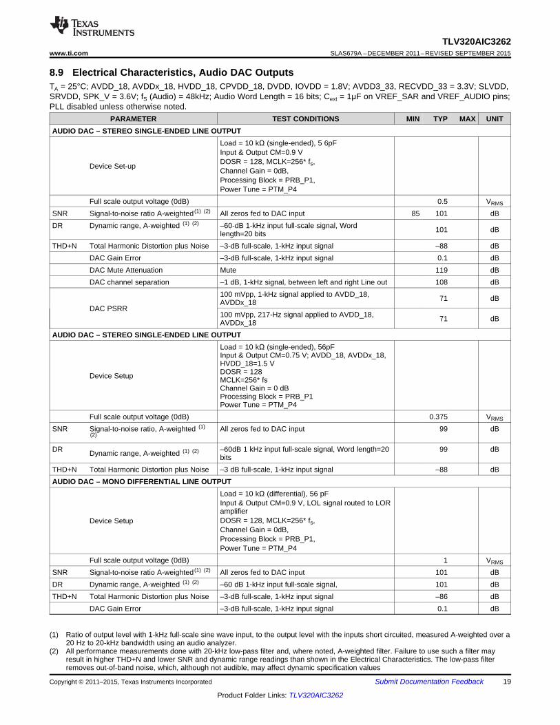
8.9 Electrical Characteristics, Audio DAC OutputsTA = 25°C; AVDD_18, AVDDx_18, HVDD_18, CPVDD_18, DVDD, IOVDD = 1.8V; AVDD3_33, RECVDD_33 = 3.3V; SLVDD,SRVDD, SPK_V = 3.6V; fS (Audio) = 48kHz; Audio Word Length = 16 bits; Cext = 1μF on VREF_SAR and VREF_AUDIO pins;PLL disabled unless otherwise noted.
PARAMETER TEST CONDITIONS MIN TYP MAX UNITAUDIO DAC – STEREO SINGLE-ENDED LINE OUTPUT
Load = 10 kΩ (single-ended), 5 6pFInput & Output CM=0.9 VDOSR = 128, MCLK=256* fs,Device Set-up Channel Gain = 0dB,Processing Block = PRB_P1,Power Tune = PTM_P4
Full scale output voltage (0dB) 0.5 VRMS
SNR Signal-to-noise ratio A-weighted (1) (2) All zeros fed to DAC input 85 101 dBDR Dynamic range, A-weighted (1) (2) –60-dB 1-kHz input full-scale signal, Word 101 dBlength=20 bitsTHD+N Total Harmonic Distortion plus Noise –3-dB full-scale, 1-kHz input signal –88 dB
DAC Gain Error –3-dB full-scale, 1-kHz input signal 0.1 dBDAC Mute Attenuation Mute 119 dBDAC channel separation –1 dB, 1-kHz signal, between left and right Line out 108 dB
100 mVpp, 1-kHz signal applied to AVDD_18, 71 dBAVDDx_18DAC PSRR
100 mVpp, 217-Hz signal applied to AVDD_18, 71 dBAVDDx_18AUDIO DAC – STEREO SINGLE-ENDED LINE OUTPUT
Load = 10 kΩ (single-ended), 56pFInput & Output CM=0.75 V; AVDD_18, AVDDx_18,HVDD_18=1.5 VDOSR = 128Device Setup MCLK=256* fsChannel Gain = 0 dBProcessing Block = PRB_P1Power Tune = PTM_P4
Full scale output voltage (0dB) 0.375 VRMS
SNR Signal-to-noise ratio, A-weighted (1) All zeros fed to DAC input 99 dB(2)
DR –60dB 1 kHz input full-scale signal, Word length=20 99 dBDynamic range, A-weighted (1) (2)bits
THD+N Total Harmonic Distortion plus Noise –3 dB full-scale, 1-kHz input signal –88 dBAUDIO DAC – MONO DIFFERENTIAL LINE OUTPUT
Load = 10 kΩ (differential), 56 pFInput & Output CM=0.9 V, LOL signal routed to LORamplifierDOSR = 128, MCLK=256* fs,Device SetupChannel Gain = 0dB,Processing Block = PRB_P1,Power Tune = PTM_P4
Full scale output voltage (0dB) 1 VRMS
SNR Signal-to-noise ratio A-weighted (1) (2) All zeros fed to DAC input 101 dBDR Dynamic range, A-weighted (1) (2) –60 dB 1-kHz input full-scale signal, 101 dBTHD+N Total Harmonic Distortion plus Noise –3-dB full-scale, 1-kHz input signal –86 dB
DAC Gain Error –3-dB full-scale, 1-kHz input signal 0.1 dB
(1) Ratio of output level with 1-kHz full-scale sine wave input, to the output level with the inputs short circuited, measured A-weighted over a20 Hz to 20-kHz bandwidth using an audio analyzer.
(2) All performance measurements done with 20-kHz low-pass filter and, where noted, A-weighted filter. Failure to use such a filter mayresult in higher THD+N and lower SNR and dynamic range readings than shown in the Electrical Characteristics. The low-pass filterremoves out-of-band noise, which, although not audible, may affect dynamic specification values
Copyright © 2011–2015, Texas Instruments Incorporated Submit Documentation Feedback 19
Product Folder Links: TLV320AIC3262

TLV320AIC3262SLAS679A –DECEMBER 2011–REVISED SEPTEMBER 2015 www.ti.com
Electrical Characteristics, Audio DAC Outputs (continued)TA = 25°C; AVDD_18, AVDDx_18, HVDD_18, CPVDD_18, DVDD, IOVDD = 1.8V; AVDD3_33, RECVDD_33 = 3.3V; SLVDD,SRVDD, SPK_V = 3.6V; fS (Audio) = 48kHz; Audio Word Length = 16 bits; Cext = 1μF on VREF_SAR and VREF_AUDIO pins;PLL disabled unless otherwise noted.
PARAMETER TEST CONDITIONS MIN TYP MAX UNITDAC Mute Attenuation Mute 97 dB
100 mVpp, 1-kHz signal applied to AVDD_18, 62 dBAVDDx_18DAC PSRR
100 mVpp, 217-Hz signal applied to AVDD_18, 63 dBAVDDx_18AUDIO DAC – STEREO SINGLE-ENDED HEADPHONE OUTPUT (GROUND-CENTERED CIRCUIT CONFIGURATION)
Load = 16 Ω (single-ended), 56 pF,Input CM=0.9 V;DOSR = 128, MCLK=256* fs,
Device Set-up Channel Gain = 0 dB,Processing Block = PRB_P1,Power Tune = PTM_P3,Headphone Output Strength=100%
Output 1 Output voltage 0.5 VRMS
SNR Signal-to-noise ratio, A-weighted (3) All zeros fed to DAC input 80 94 dB(4)
DR Dynamic range, A-weighted (3) (4) –60 dB 1-kHz input full-scale signal 93 dBTHD+N Total Harmonic Distortion plus Noise –3-dB full-scale, 1-kHz input signal –71 –55 dB
DAC Gain Error –3-dB, 1-kHz input full scale signal –0.2 dBDAC Mute Attenuation Mute 92 dBDAC channel separation –3 dB, 1-kHz signal, between left and right HP out 83 dB
100 mVpp, 1-kHz signal applied to AVDD_18, 55 dBAVDD1x_18DAC PSRR
100 mVpp, 217-Hz signal applied to AVDD_18, 55 dBAVDD1x_18Power Delivered THDN ≤ –40 dB, Load = 16 Ω 15 mW
Output 2 Output voltage Load = 16 Ω (single-ended), Channel Gain = 5 dB 0.8 VRMS
SNR Signal-to-noise ratio, A-weighted (3) (4) All zeros fed to DAC input, Load = 16 Ω 96 dBPower Delivered THDN ≤ –40 dB, Load = 16 Ω 24 mW
Output 3 Output voltage Load = 32 Ω (single-ended), Channel Gain = 5 dB 0.9 VRMS
SNR Signal-to-noise ratio, A-weighted (3) (4) All zeros fed to DAC input, Load = 32 Ω 97 dBPower Delivered THDN ≤ –40 dB, Load = 32 Ω 22 mW
AUDIO DAC – STEREO SINGLE-ENDED HEADPHONE OUTPUT (UNIPOLAR CIRCUIT CONFIGURATION)Load = 16 Ω (single-ended), 56 pFInput & Output CM=0.9 V, DOSR = 128,MCLK=256* fs, Channel Gain=0dBDevice Set-up Processing Block = PRB_P1Power Tune = PTM_P4Headphone Output Control = 100%
Full scale output voltage (0dB) 0.5 VRMS
SNR Signal-to-noise ratio, A-weighted (3) (4) All zeros fed to DAC input 100 dBDR Dynamic range, A-weighted (3) (4) –60 dB 1-kHz input full-scale signal, Power Tune = 100 dBPTM_P4THD+N Total Harmonic Distortion plus Noise –3 dB full-scale, 1-kHz input signal –79 dB
DAC Gain Error –3 dB, 1-kHz input full scale signal –0.2 dB
(3) Ratio of output level with 1-kHz full-scale sine wave input, to the output level with the inputs short circuited, measured A-weighted over a20 Hz to 20-kHz bandwidth using an audio analyzer.
(4) All performance measurements done with 20-kHz low-pass filter and, where noted, A-weighted filter. Failure to use such a filter mayresult in higher THD+N and lower SNR and dynamic range readings than shown in the Electrical Characteristics. The low-pass filterremoves out-of-band noise, which, although not audible, may affect dynamic specification values
20 Submit Documentation Feedback Copyright © 2011–2015, Texas Instruments Incorporated
Product Folder Links: TLV320AIC3262

TLV320AIC3262www.ti.com SLAS679A –DECEMBER 2011–REVISED SEPTEMBER 2015
Electrical Characteristics, Audio DAC Outputs (continued)TA = 25°C; AVDD_18, AVDDx_18, HVDD_18, CPVDD_18, DVDD, IOVDD = 1.8V; AVDD3_33, RECVDD_33 = 3.3V; SLVDD,SRVDD, SPK_V = 3.6V; fS (Audio) = 48kHz; Audio Word Length = 16 bits; Cext = 1μF on VREF_SAR and VREF_AUDIO pins;PLL disabled unless otherwise noted.
PARAMETER TEST CONDITIONS MIN TYP MAX UNITDAC Mute Attenuation Mute 119 dBDAC channel separation –1 dB, 1-kHz signal, between left and right HP out 88 dB
100 mVpp, 1-kHz signal applied to AVDD_18, 64 dBAVDD1x_18DAC PSRR
100 mVpp, 217-Hz signal applied to AVDD_18, 70 dBAVDD1x_18RL=16 Ω
Power Delivered THDN ≤ –40 dB, Input CM=0.9 V, 15 mWOutput CM=0.9 V
AUDIO DAC – STEREO SINGLE-ENDED HEADPHONE OUTPUT (UNIPOLAR CIRCUIT CONFIGURATION)Load = 16 Ω (single-ended), 56 pF,Input & Output CM=0.75 V; AVDD_18, AVDDx_18,HVDD_18=1.5 V,DOSR = 128, MCLK=256* fs,Device Set-up Channel Gain = 0 dB,Processing Block = PRB_P1,Power Tune = PTM_P4Headphone Output Control = 100%
Full scale output voltage (0dB) 0.375 VRMS
SNR Signal-to-noise ratio, A-weighted (3) (4) All zeros fed to DAC input 99 dBDR Dynamic range, A-weighted (3) (4) -60dB 1 kHz input full-scale signal 99 dBTHD+N Total Harmonic Distortion plus Noise –3-dB full-scale, 1-kHz input signal –77 dBAUDIO DAC – MONO DIFFERENTIAL RECEIVER OUTPUT
Load = 32 Ω (differential), 56 pF,Output CM=1.65 V,AVDDx_18=1.8 V, DOSR = 128MCLK=256* fs, Left DAC routed to LOL to RECP,
Device Setup LOL signal routed to LOR to RECM, Channel(Receiver Driver) Gain = 6dB for full scale outputsignal,Processing Block = PRB_P4,Power Tune = PTM_P4
Full scale output voltage (0dB) 2 VRMS
SNR Signal-to-noise ratio, A-weighted (3) (4) All zeros fed to DAC input 90 99 dBDR Dynamic range, A-weighted (3) (4) –60-dB 1-kHz input full-scale signal 97 dBTHD+N Total Harmonic Distortion plus Noise –3-dB full-scale, 1-kHz input signal –81 dB
100 mVpp, 1-kHz signal applied to AVDD_18, 56 dBAVDD1x_18DAC PSRR
100 mVpp, 217-Hz signal applied to AVDD_18, 58 dBAVDD1x_18RL=32 Ω
Power Delivered THDN ≤ –40 dB, Input CM=0.9 V, 117 mWOutput CM=1.65 V
Copyright © 2011–2015, Texas Instruments Incorporated Submit Documentation Feedback 21
Product Folder Links: TLV320AIC3262

TLV320AIC3262SLAS679A –DECEMBER 2011–REVISED SEPTEMBER 2015 www.ti.com
8.10 Electrical Characteristics, Class-D OutputsTA = 25°C; AVDD_18, AVDDx_18, HVDD_18, CPVDD_18, DVDD, IOVDD = 1.8V; AVDD3_33, RECVDD_33 = 3.3V; SLVDD,SRVDD, SPK_V = 3.6V; fS (Audio) = 48kHz; Audio Word Length = 16 bits; Cext = 1μF on VREF_SAR and VREF_AUDIO pins;PLL disabled unless otherwise noted.
PARAMETER TEST CONDITIONS MIN TYP MAX UNITDAC OUTPUT TO CLASS-D SPEAKER OUTPUT; LOAD = 8 Ω (DIFFERENTIAL), 56 pF + 33 µH
SLVDD=SRVDD=3.6, BTL measurement, DAC inputOutput voltage = 0 dBFS, class-D gain = 12 dB, THD+N ≤ –20 dB, 2.67 VRMS
CM=0.9 VSLVDD=SRVDD=3.6 V, BTL measurement, class-Dgain = 6 dB, measured as idle-channel noise, A-SNR Signal-to-noise ratio 91 dBweighted (with respect to full-scale output value of 2Vrms) (1) (2), CM=0.9 VSLVDD=SRVDD=3.6 V, BTL measurement, DACTHD Total harmonic distortion –66 dBinput = 0dBFS, class-D gain = 6dB, CM=0.9V
Total harmonic distortion SLVDD=SRVDD=3.6 V, BTL measurement, DACTHD+N –66 dB+ noise input = 0dBFS, class-D gain = 6dB, CM=0.9VSLVDD=SRVDD=3.6 V, BTL measurement, ripple on 67 dBSPKVDD = 200 mVp-p at 1 kHz, CM=0.9VPower-supply rejectionPSRR ratio (1) SLVDD=SRVDD=3.6 V, BTL measurement, ripple on 67 dBSPKVDD = 200 mVp-p at 217 Hz, CM=0.9V
Mute attenuation Analog Mute Only 102 dBSLVDD = SRVDD = 0.723.6 V
THD+N = 10%, f = 1 kHz, SLVDD = SRVDD =Class-D Gain = 12 dB, CM = 1.004.2 V0.9 V, RL = 8 ΩSLVDD = SRVDD = 1.705.5 V
PO Maximum output power WSLVDD = SRVDD = 0.583.6 V
THD+N = 1%, f = 1 kHz, SLVDD = SRVDD =Class-D Gain = 12 dB, CM = 0.804.2 V0.9 V, RL = 8 ΩSLVDD = SRVDD = 1.375.5 V
DAC OUTPUT TO CLASS-D SPEAKER OUTPUT; LOAD = 8 Ω (DIFFERENTIAL), 56 pF + 33 µHSLVDD=SRVDD=5 V, BTL measurement, DAC input
Output voltage = 0 dBFS, class-D gain = 12 dB, THD+N ≤ –20dB, 3.46 VRMSCM=0.9 VSLVDD=SRVDD=5 V, BTL measurement, class-Dgain = 6 dB, measured as idle-channel noise, A-SNR Signal-to-noise ratio 91weighted (with respect to full-scale output value of 2Vrms) (1) (2) , CM=0.9VSLVDD=SRVDD=5 V, BTL measurement, DAC inputTHD Total harmonic distortion –70= 0dBFS, class-D gain = 6 dB, CM=0.9 V
Total harmonic distortion SLVDD=SRVDD=5 V, BTL measurement, DAC inputTHD+N –70+ noise = 0dBFS, class-D gain = 6 dB, CM=0.9 VSLVDD=SRVDD=5 V, BTL measurement, ripple on 67SPKVDD = 200 mVp-p at 1 kHz, CM=0.9 VPower-supply rejectionPSRR ratio (1) SLVDD=SRVDD=5 V, BTL measurement, ripple on 67SPKVDD = 200 mVp-p at 217 Hz, CM=0.9 V
Mute attenuation Analog Mute Only 102 dBTHD+N = 10%, f = 1 kHz, SLVDD = SRVDD = 5PO Maximum output power Class-D Gain = 12 dB, CM = 1.41 WV0.9 V, RL = 8 Ω
(1) Ratio of output level with 1-kHz full-scale sine wave input, to the output level with the inputs short circuited, measured A-weighted over a20-Hz to 20-kHz bandwidth using an audio analyzer.
(2) All performance measurements done with 20-kHz low-pass filter and, where noted, A-weighted filter. Failure to use such a filter mayresult in higher THD+N and lower SNR and dynamic range readings than shown in the Electrical Characteristics. The low-pass filterremoves out-of-band noise, which, although not audible, may affect dynamic specification values.
22 Submit Documentation Feedback Copyright © 2011–2015, Texas Instruments Incorporated
Product Folder Links: TLV320AIC3262

TLV320AIC3262www.ti.com SLAS679A –DECEMBER 2011–REVISED SEPTEMBER 2015
8.11 Electrical Characteristics, MiscellaneousTA = 25°C; AVDD_18, AVDDx_18, HVDD_18, CPVDD_18, DVDD, IOVDD = 1.8V; AVDD3_33, RECVDD_33 = 3.3V; SLVDD,SRVDD, SPK_V = 3.6V; fS (Audio) = 48kHz; Audio Word Length = 16 bits; Cext = 1μF on VREF_SAR and VREF_AUDIO pins;PLL disabled unless otherwise noted.
PARAMETER TEST CONDITIONS MIN TYP MAX UNIT
REFERENCE - VREF_AUDIO
CMMode = 0 (0.9 V) 0.9Reference Voltage Settings V
CMMode = 1 (0.75 V) 0.75
Reference Noise CM=0.9 V, A-weighted, 20-Hz to 20-kHz bandwidth, 1.2 μVRMSCref = 1μF
Decoupling Capacitor 1 μF
Bias Current 99 μA
miniDSP (1)
miniDSP clock frequency - ADC DVDD = 1.26 V 37.5 MHz
miniDSP clock frequency - DAC DVDD = 1.26 V 33.0 MHz
miniDSP clock frequency - ADC DVDD = 1.65 V 59.5 MHz
miniDSP clock frequency - DAC DVDD = 1.65 V 55.0 MHz
miniDSP clock frequency - ADC DVDD = 1.71 V 62.5 MHz
miniDSP clock frequency - DAC DVDD = 1.71 V 58.0 MHz
SHUTDOWN POWER
Coarse AVdd supply turned off, All External analogDevice Set-up supplies powered and set available, No external
digital input is toggled, register values are retained.
P(total) (2) Sum of all supply currents, all supplies at 1.8 V 9.8 μWexcept for SLVDD = SRVDD = SPK_V = 3.6 V andRECVDD_33 = AVDD3_33 = 3.3 V
I(DVDD) 2.6 μA
I(IOVDD) 0.15 μA
I(AVDD1_18, AVDD2_18, AVDD4_18, 1.15 μAAVDD_18, HVDD_18, CPVDD_18)
I(RECVDD_33, AVDD3_33) 0.15 μA
I(SLVDD, SRVDD, SPK_V) 0.5 μA
(1) miniDSP clock speed is specified by design and not tested in production.(2) For further details on playback and recording power consumption, refer to Powertune section in SLAU309.
8.12 Electrical Characteristics, Logic LevelsTA = 25°C; AVDD_18, AVDDx_18, HVDD_18, CPVDD_18, DVDD, IOVDD = 1.8V; AVDD3_33, RECVDD_33 = 3.3V; SLVDD,SRVDD, SPK_V = 3.6V; fS (Audio) = 48kHz; Audio Word Length = 16 bits; Cext = 1μF on VREF_SAR and VREF_AUDIO pins;PLL disabled unless otherwise noted.
PARAMETER TEST CONDITIONS MIN TYP MAX UNITLOGIC FAMILY (CMOS)
IIH = 5 μA, IOVDD > 1.65 V 0.7 × IOVDD VVIH Logic Level IIH = 5 μA, 1.2V ≤ IOVDD <1.65 V 0.9 × IOVDD V
IIH = 5 μA, IOVDD < 1.2 V IOVDD VIIL = 5 μA, IOVDD > 1.65 V –0.3 0.3 × IOVDD V
VIL IIL = 5 μA, 1.2V ≤ IOVDD <1.65 V 0.1 × IOVDD VIIL = 5 μA, IOVDD < 1.2 V 0 VIOH = 3 mA load, IOVDD > 1.65 V 0.8 × IOVDD V
VOH IOH = 1 mA load, IOVDD < 1.65 V 0.8 × IOVDD VIOL = 3 mA load, IOVDD > 1.65 V 0.1 × IOVDD V
VOL IOL = 1 mA load, IOVDD < 1.65 V 0.1 × IOVDD VCapacitive Load 10 pF
Copyright © 2011–2015, Texas Instruments Incorporated Submit Documentation Feedback 23
Product Folder Links: TLV320AIC3262

TLV320AIC3262SLAS679A –DECEMBER 2011–REVISED SEPTEMBER 2015 www.ti.com
8.13 I2S/LJF/RJF Timing in Master Mode (see Figure 2)WCLK represents WCLK1 pin for Audio Serial Interface number 1, WCLK2 pin for Audio Serial Interface number 2, andWCLK3 pin for Audio Serial Interface number 3. BCLK represents BCLK1 pin for Audio Serial Interface number 1, BCLK2 pinfor Audio Serial Interface number 2, and BCLK3 pin for Audio Serial Interface number 3. DOUT represents DOUT1 pin forAudio Serial Interface number 1, DOUT2 pin for Audio Serial Interface number 2, and DOUT3 pin for Audio Serial Interfacenumber 3. DIN represents DIN1 pin for Audio Serial Interface number 1, DIN2 pin for Audio Serial Interface number 2, andDIN3 pin for Audio Serial Interface number 3. Specifications are at 25° C with DVDD = 1.8V and IOVDD = 1.8 V. Note: Alltiming specifications are measured at characterization but not tested at final test. The audio serial interface timingspecifications are applied to Audio Serial Interface number 1, Audio Serial Interface number 2 and Audio Serial Interfacenumber 3.
IOVDD=1.8 V IOVDD=3.3 VPARAMETER UNIT
MIN MAX MIN MAXtd(WS) WCLK delay 22 20 nstd (DO-WS) WCLK to DOUT delay (For LJF Mode only) 22 20 nstd (DO-BCLK) BCLK to DOUT delay 22 20 nsts(DI) DIN set-up 4 4 nsth(DI) DIN hold 4 4 nstr BCLK Rise time 10 8 nstf BCLK Fall time 10 8 ns
8.14 I2S/LJF/RJF Timing in Slave Mode (see Figure 3)WCLK represents WCLK1 pin for Audio Serial Interface number 1, WCLK2 pin for Audio Serial Interface number 2, andWCLK3 pin for Audio Serial Interface number 3. BCLK represents BCLK1 pin for Audio Serial Interface number 1, BCLK2 pinfor Audio Serial Interface number 2, and BCLK3 pin for Audio Serial Interface number 3. DOUT represents DOUT1 pin forAudio Serial Interface number 1, DOUT2 pin for Audio Serial Interface number 2, and DOUT3 pin for Audio Serial Interfacenumber 3. DIN represents DIN1 pin for Audio Serial Interface number 1, DIN2 pin for Audio Serial Interface number 2, andDIN3 pin for Audio Serial Interface number 3. Specifications are at 25° C with DVDD = 1.8V and IOVDD = 1.8 V. Note: Alltiming specifications are measured at characterization but not tested at final test. The audio serial interface timingspecifications are applied to Audio Serial Interface number 1, Audio Serial Interface number 2 and Audio Serial Interfacenumber 3.
IOVDD=1.8 V IOVDD=3.3 VPARAMETER UNIT
MIN MAX MIN MAXtH (BCLK) BCLK high period 30 30 nstL (BCLK) BCLK low period 30 30 nsts (WS) WCLK set-up 4 4 nsth (WS) WCLK hold 4 4 nstd (DO-WS) WCLK to DOUT delay (For LJF mode only) 22 20 nstd (DO-BCLK) BCLK to DOUT delay 22 20 nsts(DI) DIN set-up 4 4 nsth(DI) DIN hold 4 4 nstr BCLK Rise time 5 4 nstf BCLK Fall time 5 4 ns
8.15 DSP/Mono PCM Timing in Slave Mode (see Figure 5)IOVDD=1.8 V IOVDD=3.3 V
PARAMETER UNITMIN MAX MIN MAX
tH (BCLK) BCLK high period 30 30 nstL (BCLK) BCLK low period 30 30 nsts(WS) WCLK set-up 4 4 nsth(WS) WCLK hold 4 4 nstd (DO-BCLK) BCLK to DOUT delay 22 20 nsts(DI) DIN set-up 5 5 ns
24 Submit Documentation Feedback Copyright © 2011–2015, Texas Instruments Incorporated
Product Folder Links: TLV320AIC3262

TLV320AIC3262www.ti.com SLAS679A –DECEMBER 2011–REVISED SEPTEMBER 2015
DSP/Mono PCM Timing in Slave Mode (see Figure 5) (continued)IOVDD=1.8 V IOVDD=3.3 V
PARAMETER UNITMIN MAX MIN MAX
th(DI) DIN hold 5 5 nstr BCLK Rise time 5 4 nstf BCLK Fall time 5 4 ns
8.16 I2C Interface Timing (see Figure 6)STANDARD-MODE FAST-MODE
PARAMETER TEST CONDITIONS UNITMIN TYP MAX MIN TYP MAX
fSCL SCL clock frequency 0 100 0 400 kHztHD;STA Hold time (repeated) START
condition. After this period, the first 4.0 0.8 μsclock pulse is generated.
tLOW LOW period of the SCL clock 4.7 1.3 μstHIGH HIGH period of the SCL clock 4.0 0.6 μstSU;STA Set-up time for a repeated START 4.7 0.8 μsconditiontHD;DAT Data hold time: For I2C bus 0 3.45 0 0.9 μsdevicestSU;DAT Data set-up time 250 100 nstr SDA and SCL Rise Time 1000 20+0.1Cb 300 nstf SDA and SCL Fall Time 300 20+0.1Cb 300 nstSU;STO Set-up time for STOP condition 4.0 0.8 μstBUF Bus free time between a STOP 4.7 1.3 μsand START conditionCb Capacitive load for each bus line 400 400 pF
8.17 SPI Interface TimingSS = SCL pin, SCLK = GPI1 pin, MISO = GPO1 pin, and MOSI = SDA pin. Specifications are at 25° C with DVDD = 1.8 V.Specifications are at 25° C with DVDD = 1.8 V.
IOVDD=1.8V IOVDD=3.3VPARAMETER TEST CONDITIONS UNIT
MIN TYP MAX MIN TYP MAXtsck SCLK Period (1) 50 40 nstsckh SCLK Pulse width High 25 20 nstsckl SCLK Pulse width Low 25 20 nstlead Enable Lead Time 25 20 nsttrail Enable Trail Time 25 20 nstd;seqxfr Sequential Transfer Delay 25 20 nsta Slave DOUT (MISO) access time 25 20 nstdis Slave DOUT (MISO) disable time 25 20 nstsu DIN (MOSI) data set-up time 8 8 nsth;DIN DIN (MOSI) data hold time 8 8 nstv;DOUT DOUT (MISO) data valid time 20 14 nstr SCLK Rise Time 4 4 nstf SCLK Fall Time 4 4 ns
(1) These parameters are based on characterization and are not tested in production.
Copyright © 2011–2015, Texas Instruments Incorporated Submit Documentation Feedback 25
Product Folder Links: TLV320AIC3262

th(WS)
WCLK
BCLK
DOUT
DIN
tL(BCLK) tH(BCLK)
ts(WS)
td(DO-WS) td(DO-BCLK)
th(DI)ts(DI)
WCLK
BCLK
DOUT
DIN
td(DO-WS)td(DO-BCLK)
tS(DI)th(DI)
td(WS)
ttdS
ta
MSB OUT BIT 6 . . . 1 LSB OUT
tscktLead
tLag
tsckh
tsckl
trtf
tv(DOUT) tdis
MSB IN BIT 6 . . . 1 LSB IN
th(DIN)tsu
SS
SCLK
MISO
MOSI
TLV320AIC3262SLAS679A –DECEMBER 2011–REVISED SEPTEMBER 2015 www.ti.com
8.18 Dissipation RatingsPACKAGE RθJA TA POWER RATING
YZF 39.1 (TJ Max – TA)/ θJA
Figure 1. SPI Timing Diagram
Figure 2. I2S/LJF/RJF Timing in Master Mode
Figure 3. I2S/LJF/RJF Timing in Slave Mode
26 Submit Documentation Feedback Copyright © 2011–2015, Texas Instruments Incorporated
Product Folder Links: TLV320AIC3262

WCLK
BCLK
DOUT
DIN
tH(BCLK)
th(ws)
tL(BCLK)
ts(ws)th(ws)
td(DO-BCLK)
th(ws)
ts(DI)th(DI)
WCLK
BCLK
DOUT
DIN
td(WS) td(WS)
td(DO-BCLK)
ts(DI)th(DI)
TLV320AIC3262www.ti.com SLAS679A –DECEMBER 2011–REVISED SEPTEMBER 2015
Figure 4. DSP/Mono PCM Timing in Master Mode
Figure 5. DSP/Mono PCM Timing in Slave Mode
Figure 6. I2C Interface Timing Diagram
Copyright © 2011–2015, Texas Instruments Incorporated Submit Documentation Feedback 27
Product Folder Links: TLV320AIC3262

−140
−120
−100
−80
−60
−40
−20
0
0.02 0.1 1 10 20Frequency (kHz)
Am
plitu
de (
dBF
S)
G003
85
90
95
100
105
110
−10 0 10 20 30 40 50
Rin = 10k, SE
Rin = 20k, SE
Rin = 40k, SE
Rin = 10k, DE
Rin = 20k, DE
Rin = 40k, DE
Channel Gain (dB)
SN
R (
dB)
G001
−140
−120
−100
−80
−60
−40
−20
0
0.02 0.1 1 10 20Frequency (kHz)
Am
plitu
de (
dBF
S)
G002
TLV320AIC3262SLAS679A –DECEMBER 2011–REVISED SEPTEMBER 2015 www.ti.com
8.19 Typical Characteristics
8.19.1 Audio ADC Performance
Figure 7. ADC SNR vs Channel Gain Input-Referred Figure 8. ADC Single-Ended Input to ADC FFT at –3 dBr vsFrequency
Figure 9. ADC Differential Input to ADC FFT at –3 dBr vs Frequency
28 Submit Documentation Feedback Copyright © 2011–2015, Texas Instruments Incorporated
Product Folder Links: TLV320AIC3262

−80
−70
−60
−50
−40
−30
−20
−10
0
0 10 20 30 40 50 60 70
CM=0.75v,16Ohm,HVDD=CPVDD=1.5V
CM=0.9v,16Ohm,HVDD=CPVDD=1.8V
CM=0.75v,32Ohm,HVDD=CPVDD=1.5V
CM=0.9v,32Ohm,HVDD=CPVDD=1.8V
Output Power (mW)
TH
DN
−T
otal
Har
mon
ic D
isto
rtio
n+N
oise
(dB
)
G007
−100
−90
−80
−70
−60
−50
−40
−30
−20
−10
0
0 20 40 60 80 100 120 140 160 180
CM=0.75V,RECVDD=1.65V
CM=0.9V,RECVDD=1.8V
CM=1.25V,RECVDD=2.5V
CM=1.5V,RECVDD=3V
CM=1.65V,RECVDD=3.3V
Output Power (mW)
TH
DN
−T
otal
Har
mon
ic D
isto
rtio
n+N
oise
(dB
)
G008
−140
−120
−100
−80
−60
−40
−20
0
0.02 0.1 1 10 20Frequency (kHz)
Am
plitu
de (
dBr)
G013
−140
−120
−100
−80
−60
−40
−20
0
0.02 0.1 1 10 20Frequency (kHz)
Am
plitu
de (
dBr)
G006
−140
−120
−100
−80
−60
−40
−20
0
0.02 0.1 1 10 20Frequency (kHz)
Am
plitu
de (
dBr)
G004
−140
−120
−100
−80
−60
−40
−20
0
0.02 0.1 1 10 20Frequency (kHz)
Am
plitu
de (
dBr)
G005
TLV320AIC3262www.ti.com SLAS679A –DECEMBER 2011–REVISED SEPTEMBER 2015
8.19.2 Audio DAC Performance
Figure 10. DAC to Line Output FFT Amplitude at –3 dBFS Figure 11. DAC to Headphone Output (GCHP) FFTvs Frequency 10-kΩ Load Amplitude at –3 dBFS vs Frequency 16-Ω Load
Figure 12. DAC to Headphone Output (GCHP) FFT Figure 13. DAC to Differential Receiver Output FFTAmplitude at –3 dBFS vs Frequency 32-Ω Load Amplitude at –3 dBFS vs Frequency 32-Ω Load
Figure 14. Total Harmonic Distortion + Noise vs Figure 15. Total Harmonic Distortion + Noise vsHeadphone (GCHP) Output Power 9-dB Gain Differential Receiver Output Power 32-Ω Load
Copyright © 2011–2015, Texas Instruments Incorporated Submit Documentation Feedback 29
Product Folder Links: TLV320AIC3262

2.8
2.85
2.9
2.95
3
0 1 2 3 4 5 6 7Micbias Load (mA)
Mic
bias
Vol
tage
(V
)
G012
−80
−70
−60
−50
−40
−30
−20
−10
0
0 200 400 600 800 1000 1200
6dB
12dB
18dB
24dB
30
Output Power (mW)
TH
DN
−T
otal
Har
mon
ic D
isto
rtio
n+N
oise
(dB
)
G010
−80
−70
−60
−50
−40
−30
−20
−10
0
0 200 400 600 800 1000 1200 1400 1600 1800
2.7V 3.6V 4.2V 5.0V 5.5v
Output Power (mW)
TH
DN
−T
otal
Har
mon
ic D
isto
rtio
n+N
oise
(dB
)
G011
0.8 1.0 1.2 1.4 1.660
70
80
90
100
110
120
SNR
0
25
50
75
100
125
150
Output Common Mode Setting (V)
SN
R −
Sig
nal T
o N
oise
Rat
ioi (
dB)
Pow
er d
eliv
ered
(m
W)
Output Power
G009
TLV320AIC3262SLAS679A –DECEMBER 2011–REVISED SEPTEMBER 2015 www.ti.com
Audio DAC Performance (continued)
Figure 16. Differential Receiver SNR and Output Power vs Output Common Mode Setting 32-Ω Load
8.19.3 Class-D Driver Performance
Figure 17. Total Harmonic Distortion + Noise vs Output Figure 18. Total Harmonic Distortion + Noise vs OutputPower Power
Different Gain Settings, 8-Ω Load, SLVDD = SRVDD = Different SLVDD/SRVDD/SPK_V Supplies, 8-Ω Load, 12-dBSPK_V = 3.6 V Gain
8.19.4 MICBIAS Performance
Figure 19. MICBIAS Mode 2, CM = 0.9 V, AVDD3_33 OP STAGE vs Micbias Load Current
30 Submit Documentation Feedback Copyright © 2011–2015, Texas Instruments Incorporated
Product Folder Links: TLV320AIC3262

TLV320AIC3262www.ti.com SLAS679A –DECEMBER 2011–REVISED SEPTEMBER 2015
9 Parameter Measurement Information
All parameters are measured according to the conditions described in Specifications.
Copyright © 2011–2015, Texas Instruments Incorporated Submit Documentation Feedback 31
Product Folder Links: TLV320AIC3262

TLV320AIC3262SLAS679A –DECEMBER 2011–REVISED SEPTEMBER 2015 www.ti.com
10 Detailed Description
10.1 OverviewThe TLV320AIC3262 is a flexible, highly-integrated, low-power, low-voltage stereo audio codec with digitalmicrophone inputs and programmable outputs, PowerTune capabilities, selectable audio-processing blocks, fixedpredefined and parameterizable signal processing blocks, integrated PLL, and flexible digital audio interfaces. Itis intended for applications in mobile handsets, tablets, eBooks, portable navigation devices, portable mediaplayer, portable gaming systems and portable computing. Available in a 4.81 mm x 4.81 mm 81-ball WCSP(YZF) Package, the device includes an extensive register-based control of power, input and output channelconfiguration, gains, effects, pin-multiplexing, and clocks, allowing the codec to be precisely targeted to itsapplication.
The TLV320AIC3262 consists of the following blocks:• 5.6-mW Stereo Audio ADC with 93dB SNR• 2.7-mW Stereo 48kHz DAC Playback• 30-mW DirectPath Headphone Driver• 128-mW Differential Receiver Output Driver• Stereo Class-D Speaker Drivers• Programmable 12-Bit SAR ADC• SPI and I2C Control Interfaces• Three Independent Digital Audio Serial Interfaces• Programmable PLL Generator• Fully-Programmable Enhanced miniDSP with PurePath Studio Support
The TLV320AIC3262 features PowerTune to trade power dissipation versus performance. This mechanism hasmany modes that can be selected at the time of device configuration.
32 Submit Documentation Feedback Copyright © 2011–2015, Texas Instruments Incorporated
Product Folder Links: TLV320AIC3262

SPI_SELECT
IN1R/AUX2
IN2R
IN3R
IN3L
IN4L
IN2L
IN1L/AUX1
DRCAGC
DRC
tPR
tPL
AGC
Audio
Interface
Ref
MICBIAS
VREF_AUDIO
LOL
LOR
–36...0dB
–36...0dB
CP
VD
D_
18
CP
VS
S
CP
FC
PC
PF
CM
VN
EG
MICBIAS_EXT
PLL
GP
O1
GP
I1
DIN
3
GP
IO1
GP
IO2
DO
UT
3
DO
UT
2
WC
LK
2
BC
LK
2
WC
LK
1
BC
LK
1
VBAT
VREF_SAR
+
+–
–
–12, –6, 0dB
–12, –6, 0dB
WC
LK
3
BC
LK
3
MICDET Detection
MicBias Charge
Pump
PrimaryAudio Interface
SecondaryAudio IF
InterruptCtrl
DigitalMic.
SPI / I CControl Block
2
Low Freq
Clocking
B0395;04
;12, ;6, 0dB
)
ADCSignalProc.
DACSignalProc.
DACSignalProc.
ADCSignalProc.
miniDSPASRC
Dig MixerVolume
miniDSPDig MixerVolume
RightADC
LeftADC
SARADC
RightDAC
LeftDAC
0>47.5dB(0.5;dB Steps)
0>47.5dB(0.5;dB Steps)
)
–12, –6, 0dB
–12, –6, 0dB
–12, –6, 0dB
–12, –6, 0dB
–6 dB
GP
I2
MC
LK
1
MC
LK
2
DO
UT
1
TertiaryAudio IF
IN4R–6 dB
Supplies
IOV
DD
RE
CV
DD
_3
3
AV
DD
1_
18
AV
DD
2_
18
SR
VD
DS
PK
_V
AV
DD
3_
33
AV
DD
_1
8A
VD
D4
_1
8
DV
DD
SR
VS
S
SL
VD
D
HV
DD
_1
8
SL
VS
S
RE
CV
SS
IOV
SS
AV
SS
1A
VS
S2
AV
SS
3
AV
SS
DV
SS
AV
SS
4
LOL
LOR
;78...0dB
;78...0dB
MAL
MAR
;6dB
;6dB
LOL
;78...0dB
;78...0dB
;78...0dB
;78...0dBRECP
RECM
;6...29dB(1;dB Steps
;6...14dB(1;dB Steps
HPL
HPR
;78...0dB
;78...0dB
HPVSS_SENSE
6...30dB
SPKLM
SPKLP
(6;dB Steps)
6...30dB
SPKRM
SPKRP
(6;dB Steps)
);6...14dB
(1;dB Steps;12, ;6, 0dB
TEMP
VBAT
IN1R/AUX2
IN1L/AUX1
TEMPSENSOR
GP
I3
GP
I4
SC
LS
DA
RESET
Vol. Ctrl.
LOR
Pin Muxing / Clock Routing
IN1L
IN1R
SPR_IN
SPR_IN
Vol. Ctrl.
Int.
Ref.
in Adj.Ga
in Adj.Ga
DIN
1
DIN
2
TLV320AIC3262www.ti.com SLAS679A –DECEMBER 2011–REVISED SEPTEMBER 2015
10.2 Functional Block Diagram
Copyright © 2011–2015, Texas Instruments Incorporated Submit Documentation Feedback 33
Product Folder Links: TLV320AIC3262

TLV320AIC3262SLAS679A –DECEMBER 2011–REVISED SEPTEMBER 2015 www.ti.com
10.3 Feature Description
10.3.1 Digital PinsOnly a small number of digital pins are dedicated to a single function; whenever possible, the digital pins have adefault function, and also can be reprogrammed to cover alternative functions for various applications.
The fixed-function pins are hardware-control pins RESET and SPI_SELECT pin. Depending on the state ofSPI_SELECT, four pins SCL, SDA, GPO1, and GPI1 are configured for either I2C or SPI protocol. Only in I2Cmode, GPI3 and GPI4 provide four possible I2C addresses for the TLV320AIC3262.
Other digital IO pins can be configured for various functions through register control.
10.3.2 Analog PinsAnalog functions can also be configured to a large degree. For minimum power consumption, analog blocks arepowered down by default. The blocks can be powered up with fine granularity according to the application needs.
The possible analog routings of analog input pins to ADCs and output amplifiers as well as the routing fromDACs to output amplifiers can be seen in the Analog Routing Diagram.
10.3.3 Multifunction PinsTable 1 shows the possible allocation of pins for specific functions. The PLL input, for example, can beprogrammed to be any of 9 pins (MCLK1, MCLK2, BCLK1, DIN1, BCLK2, GPIO1, GPIO2, GPI1, GPI2).
Table 1. Multifunction Pin Assignments for Pins MCLK1, MCLK2, WCLK1, BCLK1, DIN1, DOUT1,WCLK2, BCLK2, DIN2, and DOUT2
1 2 3 4 5 6 7 8 9 10PIN FUNCTION MCLK1 MCLK2 WCLK1 BCLK1 DIN1 DOUT1 WCLK2 BCLK2 DIN2 DOUT2
A INT1 Output E E E EB INT2 Output E E E EC SAR ADC Interrupt E E E ED CLOCKOUT Output E E E EE ADC_MOD_CLOCK Output E E EF Single DOUT for ASI1 (All E, D
Channels)F Single DOUT for ASI2 E, DF Single DOUT for ASI3G Multiple DOUTs for ASI1 (L1, E
R1)G Multiple DOUTs for ASI1 (L2, E
R2)G Multiple DOUTs for ASI1 (L3, E
R3)G Multiple DOUTs for ASI1 (L4, E
R4)I General Purpose Output (via E (1) E E E
Reg)F Single DIN for ASI1 (All E, D (2)
Channels)F Single DIN for ASI2 E, DF Single DIN for ASI3H Multiple DINs for ASI1 (L1, E
R1)H Multiple DINs for ASI1 (L2, E
R2)
(1) E: The pin is exclusively used for this function, no other function can be implemented with the same pin (for example if DOUT1 hasbeen allocated for General Purpose Output, it cannot be used as the INT1 output at the same time)
(2) D: Default Function
34 Submit Documentation Feedback Copyright © 2011–2015, Texas Instruments Incorporated
Product Folder Links: TLV320AIC3262

TLV320AIC3262www.ti.com SLAS679A –DECEMBER 2011–REVISED SEPTEMBER 2015
Feature Description (continued)Table 1. Multifunction Pin Assignments for Pins MCLK1, MCLK2, WCLK1, BCLK1, DIN1, DOUT1, WCLK2,
BCLK2, DIN2, and DOUT2 (continued)1 2 3 4 5 6 7 8 9 10
PIN FUNCTION MCLK1 MCLK2 WCLK1 BCLK1 DIN1 DOUT1 WCLK2 BCLK2 DIN2 DOUT2H Multiple DINs for ASI1 (L3, E E
R3)H Multiple DINs for ASI1 (L4, E E
R4)J Digital Mic Data E E EK Input to PLL_CLKIN S (3), D S S (4) S S (4)
L Input to ADC_CLKIN S (3), D S S (4) S (4)
M Input to DAC_CLKIN S (3), D S S (4) S (4)
N Input to CDIV_CLKIN S (3), D S S S SO Input to LFR_CLKIN S (3), D S S S S SP Input to HF_CLK S (3)
Q Input to REF_1MHz_CLK S (3)
R General Purpose Input (via E E E EReg)
S ISR Interrupt for miniDSP E(via Reg)
T WCLK Output for ASI1 EU WCLK Input for ASI1 S, DV BCLK Output for ASI1 EW BCLK Input for ASI1 S (4), DX WCLK Output for ASI2 EY WCLK Input for ASI2 S, DZ BCLK Output for ASI2 EAA BCLK Input for ASI2 S (4), DBB WCLK Output for ASI3CC WCLK Input for ASI3DD BCLK Output for ASI3EE BCLK Input for ASI3
(3) S(3): The MCLK1 pin could be chosen to drive the PLL, ADC Clock, DAC Clock, CDIV Clock, LFR Clock, HF Clock, andREF_1MHz_CLK inputs simultaneously
(4) S(4): The BCLK1 or BCLK2 pins could be chosen to drive the PLL, ADC Clock, DAC Clock, and audio interface bit clock inputssimultaneously
Table 2. Multifunction Pin Assignments for Pins WCLK3, BCLK3, DIN3, DOUT3, GPIO1, GPIO2, GPO1,GPI1, GPI2, GPI3, and GPI4
11 12 13 14 15 16 17 18 19 20 21PIN FUNCTION WCLK3 BCLK3 DIN3 DOUT3 GPIO1 GPIO2 GPO1/ GPI1/ GPI2 GPI3 (2) GPI4 (2)
MISO (1) SCLK (1)
A INT1 Output E E EB INT2 Output E E EC SAR ADC Interrupt E E ED CLOCKOUT Output E E EE ADC_MOD_CLOCK E E E
Output
(1) GPO1 and GPI1 can only be utilized for functions defined in this table when part utilizes I2C for control. In SPI mode, these pins serveas the MISO and SCLK, respectively.
(2) GPI3 and GPI4 can only be utilized for functions defined in this table when part utilizes SPI for control. In I2C mode, these pins serve asI2C address pins.
Copyright © 2011–2015, Texas Instruments Incorporated Submit Documentation Feedback 35
Product Folder Links: TLV320AIC3262

TLV320AIC3262SLAS679A –DECEMBER 2011–REVISED SEPTEMBER 2015 www.ti.com
Table 2. Multifunction Pin Assignments for Pins WCLK3, BCLK3, DIN3, DOUT3, GPIO1, GPIO2, GPO1,GPI1, GPI2, GPI3, and GPI4 (continued)
11 12 13 14 15 16 17 18 19 20 21PIN FUNCTION WCLK3 BCLK3 DIN3 DOUT3 GPIO1 GPIO2 GPO1/ GPI1/ GPI2 GPI3 (2) GPI4 (2)
MISO (1) SCLK (1)
F Single DOUT for ASI1 E(All Channels)
F Single DOUT for ASI2F Single DOUT for ASI3 E, DG Multiple DOUTs for
ASI1 (L1, R1)G Multiple DOUTs for E E E
ASI1 (L2, R2)G Multiple DOUTs for E E E E E
ASI1 (L3, R3)G Multiple DOUTs for E E E E
ASI1 (L4, R4)I General Purpose E (3) E E E E E
Output (via Reg)F Single DIN for ASI1 E
(All Channels)F Single DIN for ASI2F Single DIN for ASI3 E, DH Multiple DINs for ASI1
(L1, R1)H Multiple DINs for ASI1 E E E
(L2, R2)H Multiple DINs for ASI1 E E E E E
(L3, R3)H Multiple DINs for ASI1 E E E E
(L4, R4)J Digital Mic Data E E E EK Input to PLL_CLKIN S (4) S (4) S (4) S (4)
L Input to ADC_CLKIN S (4) S (4) S (4) S (4)
M Input to DAC_CLKIN S (4) S (4) S (4) S (4)
N Input to CDIV_CLKIN S SO Input to LFR_CLKIN S S S S S SP Input to HF_CLKQ Input to
REF_1MHz_CLKR General Purpose Input E E E E E E E
(via Reg)S ISR Interrupt for E E E
miniDSP (via Reg)T WCLK Output for ASI1 E EU WCLK Input for ASI1 EV BCLK Output for ASI1 EW BCLK Input for ASI1 EX WCLK Output for ASI2Y WCLK Input for ASI2Z BCLK Output for ASI2AA BCLK Input for ASI2
(3) E: The pin is exclusively used for this function, no other function can be implemented with the same pin (for example if WCLK3 hasbeen allocated for General Purpose Output, it cannot be used as the ASI3 WCLK output at the same time)
(4) S(4): The GPIO1, GPIO2, GPI1, or GPI2 pins could be chosen to drive the PLL, ADC Clock, and DAC Clock inputs simultaneously
36 Submit Documentation Feedback Copyright © 2011–2015, Texas Instruments Incorporated
Product Folder Links: TLV320AIC3262

TLV320AIC3262www.ti.com SLAS679A –DECEMBER 2011–REVISED SEPTEMBER 2015
Table 2. Multifunction Pin Assignments for Pins WCLK3, BCLK3, DIN3, DOUT3, GPIO1, GPIO2, GPO1,GPI1, GPI2, GPI3, and GPI4 (continued)
11 12 13 14 15 16 17 18 19 20 21PIN FUNCTION WCLK3 BCLK3 DIN3 DOUT3 GPIO1 GPIO2 GPO1/ GPI1/ GPI2 GPI3 (2) GPI4 (2)
MISO (1) SCLK (1)
BB WCLK Output for ASI3 ECC WCLK Input for ASI3 S, D (5)
DD BCLK Output for ASI3 EEE BCLK Input for ASI3 S, DFF ADC BCLK Input for E E E E E E
ASI1GG ADC WCLK Input for E E E E E E
ASI1HH ADC BCLK Output for E E
ASI1II ADC WCLK Output for E E
ASI1JJ ADC BCLK Input for E E E E E E
ASI2KK ADC WCLK Input for E E E E E E
ASI2LL ADC BCLK Output for E E
ASI2MM ADC WCLK Output for E E
ASI2NN ADC BCLK Input for E E E E E E
ASI3OO ADC WCLK Input for E E E E E E
ASI3PP ADC BCLK Output for E E
ASI3QQ ADC WCLK Output for E E
ASI3
(5) D: Default Function
Copyright © 2011–2015, Texas Instruments Incorporated Submit Documentation Feedback 37
Product Folder Links: TLV320AIC3262

! !
!
! !
!
"!
"!
"!
"!
"!
!
#"!$%#
!
&'()
&'()
* #"
#"
* #"
!
!#
#"
+'+
!
#"!
+,+-./
'0
#"!
!#
/1
#23
*
43*
#23*
&
4
$5
#23
6&, "!
"
/
/
#"
!#
#"!
43*
#23
4!#
#"
/
/1
#23
"77
38#23
0
9!
9
+
9!
9
!#
/
!#
/
+
/
!#
++'
++
+'+'
+)+'
!:#23
!#+'+)
!:#23
*
+,+-).
+)+
+'+
++)
++
++-.
++-.
'0
'0
++-.
+)+
+'+-.
+'+)
+0+-.
++-.
+0+-).
+))+-'.
++'
"77
38#23
0
'0
'0
+)+;<
+0+-.;%
+'+;<
++-).;%
++;<
++;<
'0 ++-.
+'+-.
'0
++-).;%"
++';<"
+0+-.
'0
+,+-.
+'+
+'+
+,+-).
+),
+
==9
==9
==9
==9
==9
==9
==9
==9
==9
==9
==9
==9
==9
==9
==9
==9
>#317!$%#
%#31; 31<* ;9
%#31;& 31<*;9
%#31; 31<*;9
%#31; 31<*;9
%#31; 31<*;9
%#31; 31<*;9
++
+)+)9
9
9 +)+
9+)+
9
9
+))+-).
+))+-.
+))+-.
+)+)
+)'+-).
+)'+-.
+)'+-'.
+)'+-.
+)+-.
+)+-'.
+)+-.
+)+-).
+)+-'.
+)+-).
+)+-.
+)+-.
++-.
+0+-.
+)+;<
+0+-.;%
+'+;<
++-).;%
+'+-.
!$%#
*
+0+-).
++-.
++-.+0+-.
+,+-.
+'+-.
+'+;<
+'+;<
++-).;%"!
++;<"!
+,+-.
TLV320AIC3262SLAS679A –DECEMBER 2011–REVISED SEPTEMBER 2015 www.ti.com
10.3.4 Analog Audio I/O
For more detailed information see the TLV320AIC3262 Application Reference Guide, SLAU309.
Figure 20. Analog Routing Diagram
10.3.4.1 Analog Low Power BypassThe TLV320AIC3262 offers two analog-bypass modes. In either of the modes, an analog input signal can berouted from an analog input pin to an amplifier driving an analog output pin. Neither the ADC nor the DACresources are required for such operation; this supports low-power operation during analog-bypass mode. Inanalog low-power bypass mode, line-level signals can be routed directly from the analog inputs IN1L to the leftlineout amplifier (LOL) and IN1R to LOR. Additionally, line-level signals can be routed directly from these analoginputs to the differential receiver amplifier, which outputs on RECP and RECM.
10.3.4.2 ADC Bypass Using Mixer AmplifiersIn addition to the low-power bypass mode, there is a bypass mode that uses the programmable gain amplifiers ofthe input stage in conjunction with a mixer amplifier. With this mode, microphone-level signals can be amplifiedand routed to the line, speaker, or headphone outputs, fully bypassing the ADC and DAC. To enable this mode,the mixer amplifiers are powered on via software command.
38 Submit Documentation Feedback Copyright © 2011–2015, Texas Instruments Incorporated
Product Folder Links: TLV320AIC3262

HPL
HPR
HPVSS_SENSE
TLV320AIC3262www.ti.com SLAS679A –DECEMBER 2011–REVISED SEPTEMBER 2015
10.3.4.3 Headphone OutputsThe stereo headphone drivers on pins HPL and HPR can drive loads with impedances down to 16 Ω in single-ended DC-coupled headphone configurations. An integral charge pump generates the negative supply requiredto operate the headphone drivers in DC-coupled mode, where the common mode of the output signal is madeequal to the ground of the headphone load using a ground-sense circuit. Operation of headphone drivers in DC-coupled (ground centered mode) eliminates the need for large DC-blocking capacitors.
Figure 21. TLV320AIC3262 Ground-Centered Headphone Output
Alternatively the headphone amplifier can also be operated in a unipolar circuit configuration using DC blockingcapacitors.
10.3.4.4 Using the Headphone AmplifierThe headphone drivers are capable of driving a mixed combination of DAC signal, left and right ADC PGA signal,and LOL and LOR output signals by configuring B0_P1_R27-R29. The ADC PGA signals can be attenuated upto 36 dB before routing to headphone drivers by configuring B0_P1_R18 and B0_P1_R19. The line-outputsignals can be attenuated up to 78 dB before routing to headphone drivers by configuring B0_P1_R28 andB0_P1_R29. The level of the DAC signal can be controlled using the digital volume control of the DAC byconfiguring B0_P0_R64-R66. To control the output-voltage swing of headphone drivers, the headphone drivervolume control provides a range of –6.0 dB to +14.0 dB (1) in steps of 1 dB. These can be configured byprogramming B0_P1_R27, B0_P1_R31, and B0_P1_R32. In addition, finer volume controls are also availablewhen routing LOL or LOR to the headphone drivers by controlling B0_P1_R27-R28. These level controls are notmeant to be used as dynamic volume control, but more to set output levels during initial device configuration.Register B0_P1_R9_D[6:5] allows the headphone output stage to be scaled to tradeoff power delivered versusquiescent power consumption. (1)
10.3.4.5 Ground-Centered Headphone Amplifier ConfigurationAmong the other advantages of the ground-centered connection is inherent freedom from turnon transients thatcan cause audible pops, sometimes at uncomfortable volumes.
(1) If the device must be placed into 'mute' from the –6.0-dB setting, set the device at a gain of –5.0 dB first, then place the device intomute.
Copyright © 2011–2015, Texas Instruments Incorporated Submit Documentation Feedback 39
Product Folder Links: TLV320AIC3262

!!"
!!"
#$#!!
%%&'
%%&'
TLV320AIC3262SLAS679A –DECEMBER 2011–REVISED SEPTEMBER 2015 www.ti.com
10.3.4.6 Circuit TopologyThe power supply hook up scheme for the ground centered configuration is shown in HVDD_18 pin supplies thepositive side of the headphone amplifier. CPVDD_18 pin supplies the charge pump which in turn supplies thenegative side of the headphone amplifier. Two capacitors are required for the charge pump circuit to work. Thesecapacitors should be X7R rated.
Figure 22. Ground-Centered Headphone Connections
10.3.4.7 Charge Pump Set-Up and OperationThe built-in charge pump draws charge from the CPVDD_18 supply, and by switching the external capacitorbetween CPFCP and CPFCM, generates the negative voltage on VNEG pin. The charge-pump circuit uses theprinciples of switched-capacitor charge conservation to generate the VNEG supply in a very efficient fashion.
To turn on the charge pump circuit when headphone drivers are powered, program B0_P1_R35_D[1:0] to 00.When the charge pump circuit is disabled, VNEG acts as a ground pin, allowing unipolar configuration of theheadphone amps. By default, the charge pump is disabled. The switching rate of the charge pump can becontrolled by B0_P1_R33. Because the charge pump can demand significant inrush currents from the supply, itis important to have a capacitor connected in close proximity to the CPVDD_18 and CPVSS pins of the device.At 500-kHz clock rate this requires approximately a 10-μF capacitor. The ESR and ESL of the capacitor must below to allow fast switching currents.
The ground-centered mode of operation is enabled by configuring B0_P1_R31_D7 to 1. The HPL and HPR gainsettings are ganged in Ground-Cetered Mode of operation (B0_P1_R32_D7 = 1). The HPL and HPR gainsettings cannot be ganged if using the Stereo Unipolar Configuration.
10.3.4.8 Output Power OptimizationThe device can be optimized for a specific output-power range. The charge pump and the headphone drivercircuitry can be reduced in power so less overall power is consumed. The headphone driver power can beprogrammed in B0_P1_R9. The control of charge pump switching current is programmed in B0_P1_R34_D[4:2].
10.3.4.9 Offset Correction and Start-UpThe TLV320AIC3262 offers an offset-correction scheme that is based on calibration during power up. Thisscheme minimizes the differences in DC voltage between HPVSS_SENSE and HPL/HPR outputs.
The offset calibration happens after the headphones are powered up in ground-centered configuration. All otherheadphone configurations like signal routings, gain settings, and mute removal must be configured beforeheadphone power-up. Any change in these settings while the headphones are powered up may result inadditional offsets and are best avoided.
40 Submit Documentation Feedback Copyright © 2011–2015, Texas Instruments Incorporated
Product Folder Links: TLV320AIC3262

TLV320AIC3262www.ti.com SLAS679A –DECEMBER 2011–REVISED SEPTEMBER 2015
The offset-calibration block has a few programmable parameters that the user must control. The user can eitherchoose to calibrate the offset only for the selected input routing or all input configurations. The calibration data isstored in internal memory until the next hardware reset or until AVDDx power is removed.
Programming B0_P1_R34_D[1:0] as 10 causes the offset to be calibrated for the selected input mode.Programming B0_P1_R34_D[1:0] as 11 causes the offset to be calibrated for all possible configurations. Allrelated blocks must be powered while doing offset correction.
Programming B0_P1_R34_D[1:0] as 00 (default) disables the offset correction block. While the offset is beingcalibrated, no signal should be applied to the headphone amplifier, that is the DAC should be kept muted andanalog bypass routing should be kept at the highest attenuation.
10.3.4.10 Ground-Centered Headphone SetupThere are four practical device setups for ground-centered operation, shown in Table 3:
Table 3. Ground-Centered Headphone Setup Performance OptionsAUDIO HIGH PERFORMANCE LOW POWER CONSUMPTION
OUTPUT16Ω 32Ω 600Ω 16Ω 32Ω 600ΩPOWER
SNR 94 dB 97 dB 98 dB 91 dB 94 dB 95 dBOutput Power 25 mW 22 mW 1.4mW 24 mW 23 mW 1.5mW
High Idle Power 23 mW 21 mW 19mW 20 mW 15 mW 12 mWConsumptionHigh-Output, High-Performance Setup High-Output, Low-Power Setup
SNR 92.5 dB 93 dB 93.5 dB 80.5 dB 85.5 dB 85.5 dBOutput Power 16 mW 8.5 mW 0.5 mW 0.9 mW 1.5mW 0.1 mW
Medium Idle Power 14 mW 12 mW 9.7 mW 8.0 mW 6.6mW 5.1 mWConsumptionMedium-Output, High-Performance Setup Medium-Output, Low-Power Setup
10.3.4.10.1 High Audio Output Power, High Performance Setup
This setup describes the register programming necessary to configure the device for a combination of high audiooutput power and high performance. To achieve this combination the parameters must be programmed to thevalues in Table 4. For the full setup script, see Table 4.
Table 4. Setup A - High Audio Output Power, High PerformancePARAMETER VALUE PROGRAMMING
CM 0.9 B0_P1_R8_D2 = "0"PTM PTM_P3 B0_P1_R3_D[4:2] = "000", B0_P1_R4_D[4:2] = "000"Processing Block 1 to 6,22,23,24 B0_P0_R60_D[4:0]DAC OSR 128 B0_P0_R13 = 0x00, B0_P0_R14 = 0x80HP sizing 100 B0_P1_R9_D[6:5] = "00"Gain 5dB B0_P1_R31 = 0x85, B0_P1_R32 = 0x85DVDD 1.8 Apply 1.26 to 1.95VAVDDx_18, HVDD_18, 1.8 Apply 1.8 to 1.95VCPVDD_18
Copyright © 2011–2015, Texas Instruments Incorporated Submit Documentation Feedback 41
Product Folder Links: TLV320AIC3262

TLV320AIC3262SLAS679A –DECEMBER 2011–REVISED SEPTEMBER 2015 www.ti.com
10.3.4.10.2 High Audio Output Power, Low Power Consumption Setup
This setup describes the register programming necessary to configure the device for a combination of high audiooutput power and low power consumption. To achieve this combination the parameters must be programmed tothe values in Table 5. For the full setup script, see Table 5.
Table 5. Setup B - High Audio Output Power, Low Power ConsumptionPARAMETER VALUE PROGRAMMING
CM 0.75 B0_P1_R8_D2 = "1"PTM PTM_P2 B0_P1_R3_D[4:2] = "001", B0_P1_R4_D[4:2] = "001"Processing Block 7 to 16 B0_P0_R60_D[4:0]DAC OSR 64 B0_P0_R13 = 0x00, B0_P0_R14 = 0x40HP sizing 100 B0_P1_R9_D[6:5] = "00"Gain 12dB B0_P1_R31 = 0x8c, B0_P1_R32 = 0x8cDVDD 1.26 Apply 1.26 to 1.95VAVDDx_18, HVDD_18, 1.8 Apply 1.5 to 1.95VCPVDD_18
10.3.4.10.3 Medium Audio Output Power, High Performance Setup
This setup describes the register programming necessary to configure the device for a combination of mediumaudio output power and high performance. To achieve this combination the parameters must be programmed tothe values in Table 6. For the full setup script, see Table 6.
Table 6. Setup C - Medium Audio Output Power, High PerformancePARAMETER VALUE PROGRAMMING
CM 0.75 B0_P1_R8_D2 = "1"PTM PTM_P2 B0_P1_R3_D[4:2] = "001", B0_P1_R4_D[4:2] = "001"Processing Block 7 to 16 B0_P0_R60_D[4:0]DAC OSR 64 B0_P0_R13 = 0x00, B0_P0_R14 = 0x40HP sizing 100 B0_P1_R9_D[6:5] = "00"Gain 7dB B0_P1_R31 = 0x87, B0_P1_R32 = 0x87DVDD 1.26 Apply 1.26 to 1.95VAVDDx_18, HVDD_18, 1.5 Apply 1.8 to 1.95VCPVDD_18
10.3.4.10.4 Lowest Power Consumption, Medium Audio Output Power Setup
This setup describes the register programming necessary to configure the device for a combination of mediumaudio output power and lowest power consumption. To achieve this combination the parameters must beprogrammed to the values in Table 7. For the full setup script, see Table 7.
Table 7. Setup D - Lowest Power Consumption, Medium Audio Output PowerPARAMETER VALUE PROGRAMMING
CM 0.75 B0_P1_R8_D2 = "1"PTM PTM_P1 B0_P1_R3_D[4:2] = "010", B0_P1_R4_D[4:2] = "010"Processing Block 26 B0_P0_R60_D[4:0] = "1 1010"DAC OSR 64 B0_P0_R13 = 0x00, B0_P0_R14 = 0x40HP sizing 25 B0_P1_R9_D[6:5] = "11"Gain 10dB B0_P1_R31 = 0x8a , B0_P1_R32 = 0x8aDVdd 1.26 Apply 1.26 to 1.95VAVDDx_18, HVDD_18, 1.5 Apply 1.5 to 1.95VCPVDD_18
42 Submit Documentation Feedback Copyright © 2011–2015, Texas Instruments Incorporated
Product Folder Links: TLV320AIC3262

Rload
Rpop
CcOutputDriver
PAD
-6...+14dB
1dB steps
-6...+14dB
1dB steps
HPL
HPR
Charge
Pump (disabled)
HPVSS_Sense
VNEG
CPFCP
CPFCM
HVDD_18
CPVSS
DVDD_18
1.5...3.6V
DVDD
DVdd
TLV320AIC3262www.ti.com SLAS679A –DECEMBER 2011–REVISED SEPTEMBER 2015
10.3.4.11 Stereo Unipolar Configuration
10.3.4.11.1 Circuit Topology
The power supply hook up scheme for the unipolar configuration is shown in Figure 23. HVDD_18 terminalsupplies the positive side of the headphone amplifier. The negative side is connected to ground potential(VNEG). It is recommended to connect the CPVDD_18 terminal to DVdd, although the charge pump must not beenabled while the device is connected in unipolar configuration.
Figure 23. Unipolar Stereo Headphone Circuit
The left and right DAC channels are routed to the corresponding left and right headphone amplifier. Thisconfiguration is also used to drive line-level loads. To enable cap-coupled mode, B0_P1_R31_D7 should be setto 0. Note that the recommended range for the HVDD_18 supply in cap-coupled mode (1.65V-3.6V) is differentthan the recommended range for the default ground-centered configuration (1.5V-1.95V). In cap-coupled modeonly, the Headphone output common mode can be controlled by changing B0_P1_R8_D[4:3].
10.3.4.11.2 Unipolar Turn-On Transient (Pop) Reduction
The TLV320AIC3262 headphone drivers also support pop-free operation in unipolar, ac-coupled configuration.Because the HPL and HPR are high-power drivers, pop can result due to sudden transient changes in the outputdrivers if care is not taken. The most critical care is required while using the drivers as stereo single-endedcapacitively-coupled drivers as shown in Figure 23. The output drivers achieve pop-free power-up by using slowpower-up modes. Conceptually, the circuit during power-up can be visualized as
Figure 24. Conceptual Circuit for Pop-Free Power-up
The value of Rpop can be chosen by setting register B0_P1_R11_D[1:0].
Copyright © 2011–2015, Texas Instruments Incorporated Submit Documentation Feedback 43
Product Folder Links: TLV320AIC3262

cmpopload
loadload V
RR
RV ´
+
=
TLV320AIC3262SLAS679A –DECEMBER 2011–REVISED SEPTEMBER 2015 www.ti.com
Table 8. Rpop Values (External Cc = 47uF)B0_P1_R11_D[1:0] Rpop VALUE
10 2 kΩ01 6 kΩ00 25 kΩ
To minimize audible artifacts, two parameters can be adjusted to match application requirements. The voltageVload across Rload at the beginning of slow charging should not be more than a few mV. At that time the voltageacross Rload can be determined as:
(1)
For a typical Rload of 32Ω, Rpop of 6 kΩ or 25 kΩ will deliver good results (see Table 8 for register settings).
According to the conceptual circuit in Figure 24, the voltage on PAD will exponentially settle to the outputcommon-mode voltage based on the value of Rpop and Cc. Thus, the output drivers must be in slow power-upmode for time T, such that at the end of the slow power-on period, the voltage on Vpad is very close to thecommon-mode voltage. The TLV320AIC3262 allows the time T to be adjusted to allow for a wide range of Rloadand Cc by programming B0_P1_R11_D[5:2]. For the time adjustments, the value of Cc is assumed to be 47μF.N=5 is expected to yield good results.
Table 9. N Values (External Cc = 47 µF)B0_P1_R11_D[5:2] Slow Charging Time = N * RC_Time_Constant (for Rpop and Cc =
47μF)0000 N=00001 N=0.50010 N=0.6250011 N=0.750100 N=0.8750101 N=1.00110 N=2.00111 N=3.01000 N=4.01001 N=5.0 (Typical Value)1010 N=6.01011 N=7.01100 N=8.01101 N=16 (Not valid for Rpop=25kΩ)1110 N=24 (Not valid for Rpop=25kΩ)1111 N=32 (Not valid for Rpop=25kΩ)
Again, for example, for Rload=32Ω, Cc=47μF and common mode of 0.9V, the number of time constants requiredfor pop-free operation is 5 or 6. A higher or lower Cc value will require higher or lower value for N.
During the slow-charging period, no signal is routed to the output driver. Therefore, choosing a larger thannecessary value of N results in a delay from power-up to signal at output. At the same time, choosing N to besmaller than the optimal value results in poor pop performance at power-up.
The signals being routed to headphone drivers (for example DAC, MAL, MAR, and IN1) often have DC offsetsdue to less-than-ideal processing. As a result, when these signals are routed to output drivers, the offset voltagecauses a pop. To improve the pop-performance in such situations, a feature is provided to soft-step the DC-offset. At the beginning of the signal routing, a high-value attenuation can be applied which can be progressivelyreduced in steps until the desired gain in the channel is reached. The time interval between each of these gainchanges can be controlled by programming B0_P1_R11_D[7:6]. This gain soft-stepping is applied only during theinitial routing of the signal to the output driver and not during subsequent gain changes.
44 Submit Documentation Feedback Copyright © 2011–2015, Texas Instruments Incorporated
Product Folder Links: TLV320AIC3262

LEFT
DAC
HPL
HPR
LEFT_DACP
LEFT_DACM
TLV320AIC3262www.ti.com SLAS679A –DECEMBER 2011–REVISED SEPTEMBER 2015
Table 10. Soft-Stepping Step TimeB0_P1_R11_D[7:6] SOFT-STEPPING STEP TIME DURING INITIAL SIGNAL ROUTING
00 0 ms (soft-stepping disabled)01 50ms10 100ms11 200ms
It is recommended to use the following sequence for achieving optimal pop performance at power-up:1. Choose the value of Rpop, N (time constants) and soft-stepping step time for slow power-up.2. Choose the configuration for output drivers, including common modes and output stage power connections3. Select the signals to be routed to headphones.4. Power-up the blocks driving signals into HPL and HPR, but keep it muted5. Unmute HPL and HPR and set the desired gain setting.6. Power-on the HPL and HPR drivers.7. Unmute the block driving signals to HPL and HPR after the Driver PGA flags are set to indicate completion of
soft-stepping after power-up. These flags can be read from B0_P1_R63_D[7:6].
It is important to configure the Headphone Output driver depop control registers before powering up theheadphone; these register contents should not be changed when the headphone drivers are powered up.
Before powering down the HPL and HPR drivers, it is recommended that user read back the flags inB0_P1_R63. For example. before powering down the HPL driver, ensure that bit B0_P1_R63_D7 = 1 and bitB0_P1_R64_D7 = 1 if LOL is routed to HPL and bit B0_P1_R65_D5 = 1 if the Left Mixer is routed to HPL. Theoutput driver should be powered down only after a steady-state power-up condition has been achieved. Thissteady state power-up condition also must be satisfied for changing the HPL/R driver mute control (setting bothB0_P1_R31_D[5:0] and B0_P1_R32_D[5:0] to "11 1001"), that is, muting and unmuting should be done after thegain and volume controls associated with routing to HPL/R finished soft-stepping.
In the differential configuration of HPL and HPR, when no coupling capacitor is used, the slow charging methodfor pop-free performance need not be used. In the differential load configuration for HPL and HPR, it isrecommended to not use the output driver MUTE feature, because a pop may result.
During the power-down state, the headphone outputs are weakly pulled to ground using an approximately 50kΩresistor to ground, to maintain the output voltage on HPL and HPR terminals.
10.3.4.12 Mono Differential DAC to Mono Differential Headphone Output
Figure 25. Low Power Mono DAC to Differential Headphone
This configuration, available in unipolar configuration of the HP amplifier supplies, supports the routing of the twodifferential outputs of the mono, left channel DAC to the headphone amplifiers in differential mode(B0_P1_R27_D5 = 1 and B0_P1_R27_D2 = 1).
Copyright © 2011–2015, Texas Instruments Incorporated Submit Documentation Feedback 45
Product Folder Links: TLV320AIC3262

TLV320AIC3262SLAS679A –DECEMBER 2011–REVISED SEPTEMBER 2015 www.ti.com
10.3.4.13 Stereo Line OutputsThe stereo line level drivers on LOL and LOR terminals can drive a wide range of line level resistive impedancesin the range of 600Ω 10 kΩ. The output common mode of line level drivers can be configured to equal the analoginput common-mode setting, either 0.75V or 0.9V. The line-level drivers can drive out a mixed combination ofDAC signal and attenuated ADC PGA signal, and signal mixing is register-programmable.
10.3.4.14 Line Out Amplifier ConfigurationsSignal mixing can be configured by programming B0_P1_R22 and B0_P1_R23. To route the output of Left DACand Right DAC for stereo single-ended output, as shown in Figure 26, LDACM can be routed to LOL driver bysetting B0_P1_R22_D7 = 1, and RDACM can be routed to LOR driver by setting B0_P1_R22_D6 = 1.Alternatively, stereo single-ended signals can also be routed through the mixer amplifiers by configuringB0_P1_R23_D[7:6]. For lowest-power operation, stereo single-ended signals can also be routed in direct pinbypass with possible gains of 0 dB, –6 dB, or –12 dB by configuring B0_P1_R23_D[4:3] and B0_P1_R23_D[1:0].While each of these two bypass cases could be used in a stereo single-ended configuration, a mono differentialinput signal could also be used.
The output of the stereo line out drivers can also be routed to the stereo headphone drivers, with 0 dB to –72-dBgain controls in steps of 0.5 dB on each headphone channel. This enables the DAC output or bypass signals tobe simultaneously played back to the stereo headphone drivers as well as stereo line-level drivers. This routingand volume control is achieved in B0_P1_R28 and B0_P1_R29.
Figure 26. Stereo Single-Ended Lineout
Additionally, the two line-level drivers can be configured to act as a mono differential line level driver by routingthe output of LOL to LOR (B0_P1_R22_D2 = 1). This differential signal takes either LDACM, MAL, or IN1L-B asa single-ended mono signal and creates a differential mono output signal on LOL and LOR.
Figure 27. Single Channel Input to Differential Lineout46 Submit Documentation Feedback Copyright © 2011–2015, Texas Instruments Incorporated
Product Folder Links: TLV320AIC3262

TLV320AIC3262www.ti.com SLAS679A –DECEMBER 2011–REVISED SEPTEMBER 2015
For digital outputs from the DAC, the two line-level drivers can be fed the differential output signal from the RightDAC by configuring B0_P1_R22_D5 = ‘1’.
Figure 28. Mono DAC Output to Differential Line-out
10.3.4.15 Differential Receiver OutputThe differential receiver amplifier output spans the RECP and RECM pins and can drive a 32-Ω receiver driver.With output common-mode setting of 1.65V and RECVDD_33 supply at 3.3V, the receiver driver can drive up toa 1-Vrms output signal. With the RECVDD_33 supply at 3.3V, the receiver driver can deliver greater than128mW into a 32Ω BTL load. If desired, the RECVDD_33 supply can be set to 1.8V, at which the driver candeliver about 40mW into the 32Ω BTL load.
10.3.4.16 Stereo Class-D Speaker OutputsThe integrated Class-D stereo speaker drivers (SPKLP/SPKLN and SPKRP/SPKRN) are capable of driving two8Ω differential loads. The speaker drivers can be powered directly from the power supply (2.7V to 5.5V) on theSLVDD and SRVDD terminals, however the voltage (including spike voltage) must be limited below the AbsoluteMaximum Voltage of 6.0V.
The speaker drivers are capable of supplying 750 mW per channel at 10% THD+N with a 3.6-V power supplyand 1.46 W per channel at 10% THD+N with a 5-V power supply. Separate left and right channels can be sent toeach Class-D driver through the Lineout signal path, or from the mixer amplifiers in the ADC bypass. If only onespeaker is being utilized for playback, the analog mixer before the Left Speaker amplifier can sum the left andright audio signals for monophonic playback.
10.3.5 ADC / Digital Microphone InterfaceThe TLV320AIC3262 includes a stereo audio ADC, which uses a delta-sigma modulator with a programmableoversampling ratio, followed by a digital decimation filter and a programmable miniDSP. The ADC supportssampling rates from 8 kHz to 192 kHz. In order to provide optimal system power management, the stereorecording path can be powered up one channel at a time, to support the case where only mono record capabilityis required.
The ADC path of the TLV320AIC3262 features a large set of options for signal conditioning as well as signalrouting:• 2 ADCs• 8 analog inputs which can be mixed and/or multiplexed in single-ended and/or differential configuration• 2 programmable gain amplifiers (PGA) with a range of 0 to +47.5dB• 2 mixer amplifiers for analog bypass• 2 low power analog bypass channels• Fine gain adjust of digital channels with 0.1-dB step size• Digital volume control with a range of –12 to +20 dB• Mute function• Automatic gain control (AGC)
In addition to the standard set of ADC features the TLV320AIC3262 also offers the following special functions:• Built-in microphone biases• Stereo digital microphone interface
Copyright © 2011–2015, Texas Instruments Incorporated Submit Documentation Feedback 47
Product Folder Links: TLV320AIC3262

TLV320AIC3262SLAS679A –DECEMBER 2011–REVISED SEPTEMBER 2015 www.ti.com
– Allows 2 total microphones– Up to 2 digital microphones– Up to 2 analog microphones
• Channel-to-channel phase adjustment• Fast charge of ac-coupling capacitors• Anti thump• Adaptive coefficient update mode
10.3.5.1 ADC Processing Blocks – OverviewThe TLV320AIC3262 ADC channel includes a built-in digital decimation filter to process the oversampled datafrom the sigma-delta modulator to generate digital data at Nyquist sampling rate with high dynamic range. Thedecimation filter can be chosen from three different types, depending on the required frequency response, groupdelay, and sampling rate.
10.3.5.1.1 ADC Processing Blocks
The TLV320AIC3262 offers a range of processing blocks which implement various signal processing capabilitiesalong with decimation filtering. These processing blocks give users the choice of how much and what type ofsignal processing they may use and which decimation filter is applied.
The choice between these processing blocks is part of the PowerTune strategy to balance power conservationand signal-processing flexibility. Decreasing the use of signal-processing capabilities reduces the powerconsumed by the device. Table 11 gives an overview of the available processing blocks of the ADC channel andtheir properties. The Resource Class Column (RC) gives an approximate indication of power consumption.
The signal processing blocks available is:• First-order IIR• Scalable number of biquad filters• Variable-tap FIR filter• AGC
The processing blocks are tuned for common cases and can achieve high anti-alias filtering or low-group delay incombination with various signal processing effects such as audio effects and frequency shaping. The availablefirst order IIR, BiQuad and FIR filters have fully user programmable coefficients.
48 Submit Documentation Feedback Copyright © 2011–2015, Texas Instruments Incorporated
Product Folder Links: TLV320AIC3262

TLV320AIC3262www.ti.com SLAS679A –DECEMBER 2011–REVISED SEPTEMBER 2015
Table 11. ADC Processing BlocksProcessing Channel Decimation 1st Order Number FIR Required AOSR Resource
Blocks ValueFilter IIR Available BiQuads ClassPRB_R1 (1) Stereo A Yes 0 No 128,64,32,16,8,4 7PRB_R2 Stereo A Yes 5 No 128,64,32,16,8,4 8PRB_R3 Stereo A Yes 0 25-Tap 128,64,32,16,8,4 8PRB_R4 Left A Yes 0 No 128,64,32,16,8,4 4PRB_R5 Left A Yes 5 No 128,64,32,16,8,4 4PRB_R6 Left A Yes 0 25-Tap 128,64,32,16,8,4 4PRB_R7 Stereo B Yes 0 No 64,32,16,8,4,2 3PRB_R8 Stereo B Yes 3 No 64,32,16,8,4,2 4PRB_R9 Stereo B Yes 0 17-Tap 64,32,16,8,4,2 4PRB_R10 Left B Yes 0 No 64,32,16,8,4,2 2PRB_R11 Left B Yes 3 No 64,32,16,8,4,2 2PRB_R12 Left B Yes 0 17-Tap 64,32,16,8,4,2 2PRB_R13 Stereo C Yes 0 No 32,16,8,4,2,1 3PRB_R14 Stereo C Yes 5 No 32,16,8,4,2,1 4PRB_R15 Stereo C Yes 0 25-Tap 32,16,8,4,2,1 4PRB_R16 Left C Yes 0 No 32,16,8,4,2,1 2PRB_R17 Left C Yes 5 No 32,16,8,4,2,1 2PRB_R18 Left C Yes 0 25-Tap 32,16,8,4,2,1 2
(1) Default
For more detailed information see the TLV320AIC3262 Applications Reference Guide, SLAU309.
Copyright © 2011–2015, Texas Instruments Incorporated Submit Documentation Feedback 49
Product Folder Links: TLV320AIC3262

TLV320AIC3262SLAS679A –DECEMBER 2011–REVISED SEPTEMBER 2015 www.ti.com
10.3.6 DACThe TLV320AIC3262 includes a stereo audio DAC supporting data rates from 8 kHz to 192 kHz. Each channel ofthe stereo audio DAC consists of a signal-processing engine with fixed processing blocks, a programmableminiDSP, a digital interpolation filter, multi-bit digital delta-sigma modulator, and an analog reconstruction filter.The DAC is designed to provide enhanced performance at low sampling rates through increased oversamplingand image filtering, thereby keeping quantization noise generated within the delta-sigma modulator and signalimages strongly suppressed within the audio band to beyond 20kHz. To handle multiple input rates and optimizepower dissipation and performance, the TLV320AIC3262 allows the system designer to program theoversampling rates over a wide range from 1 to 1024. The system designer can choose higher oversamplingratios for lower input data rates and lower oversampling ratios for higher input data rates.
The TLV320AIC3262 DAC channel includes a built-in digital interpolation filter to generate oversampled data forthe sigma-delta modulator. The interpolation filter can be chosen from three different types depending onrequired frequency response, group delay and sampling rate.
The DAC path of the TLV320AIC3262 features many options for signal conditioning and signal routing:• 2 headphone amplifiers
– Usable in single-ended stereo or differential mono mode– Analog volume setting with a range of -6 to +14 dB
• 2 line-out amplifiers– Usable in single-ended stereo or differential mono mode
• 2 Class-D speaker amplifiers– Usable in stereo differential mode– Analog volume control with a settings of +6, +12, +18, +24, and +30 dB
• 1 Receiver amplifier– Usable in mono differential mode– Analog volume setting with a range of -6 to +29 dB
• Digital volume control with a range of -63.5 to +24dB• Mute function• Dynamic range compression (DRC)
In addition to the standard set of DAC features the TLV320AIC3262 also offers the following special features:• Built in sine wave generation (beep generator)• Digital auto mute• Adaptive coefficient update mode• Asynchronous Sample Rate Conversion
10.3.6.1 DAC Processing Blocks — Overview
10.3.6.1.1 DAC Processing Blocks
The TLV320AIC3262 implements signal processing capabilities and interpolation filtering through processingblocks. These fixed processing blocks give users the choice of how much and what type of signal processingthey may use and which interpolation filter is applied.
The choice between these processing blocks is part of the PowerTune strategy balancing power conservationand signal processing flexibility. Less signal processing capability will result in less power consumed by thedevice. Table 12 gives an overview over all available processing blocks of the DAC channel and their properties.The Resource Class Column (RC) gives an approximate indication of power consumption.
The signal processing blocks available are:• First-order IIR• Scalable number of biquad filters• 3D – Effect• Beep Generator
50 Submit Documentation Feedback Copyright © 2011–2015, Texas Instruments Incorporated
Product Folder Links: TLV320AIC3262

TLV320AIC3262www.ti.com SLAS679A –DECEMBER 2011–REVISED SEPTEMBER 2015
The processing blocks are tuned for common cases and can achieve high image rejection or low group delay incombination with various signal processing effects such as audio effects and frequency shaping. The availablefirst-order IIR and biquad filters have fully user-programmable coefficients.
Table 12. Overview – DAC Predefined Processing BlocksProcessing Interpolation Channel 1st Order Num. of DRC 3D Beep RC ClassBlock No. Filter IIR Available Biquads GeneratorPRB_P1 (1) A Stereo No 3 No No No 8PRB_P2 A Stereo Yes 6 Yes No No 12PRB_P3 A Stereo Yes 6 No No No 10PRB_P4 A Left No 3 No No No 4PRB_P5 A Left Yes 6 Yes No No 6PRB_P6 A Left Yes 6 No No No 5PRB_P7 B Stereo Yes 0 No No No 5PRB_P8 B Stereo No 4 Yes No No 9PRB_P9 B Stereo No 4 No No No 7PRB_P10 B Stereo Yes 6 Yes No No 9PRB_P11 B Stereo Yes 6 No No No 7PRB_P12 B Left Yes 0 No No No 3PRB_P13 B Left No 4 Yes No No 4PRB_P14 B Left No 4 No No No 4PRB_P15 B Left Yes 6 Yes No No 5PRB_P16 B Left Yes 6 No No No 4PRB_P17 C Stereo Yes 0 No No No 3PRB_P18 C Stereo Yes 4 Yes No No 6PRB_P19 C Stereo Yes 4 No No No 4PRB_P20 C Left Yes 0 No No No 2PRB_P21 C Left Yes 4 Yes No No 3PRB_P22 C Left Yes 4 No No No 2PRB_P23 A Stereo No 2 No Yes No 8PRB_P24 A Stereo Yes 5 Yes Yes No 12PRB_P25 A Stereo Yes 5 Yes Yes Yes 13PRB_P26 D Stereo No 0 No No No 1
(1) Default
For more detailed information see the TLV320AIC3262 Applications Reference Guide, SLAU309.
10.3.7 PowertuneThe TLV320AIC3262 features PowerTune, a mechanism to balance power-versus-performance trade-offs at thetime of device configuration. The device can be tuned to minimize power dissipation, to maximize performance,or to an operating point between the two extremes to best fit the application. The TLV320AIC3262 PowerTunemodes are called PTM_R1 to PTM_R4 for the recording (ADC) path and PTM_P1 to PTM_P4 for the playback(DAC) path.
For more detailed information see the TLV320AIC3262 Applications Reference Guide, SLAU309.
Copyright © 2011–2015, Texas Instruments Incorporated Submit Documentation Feedback 51
Product Folder Links: TLV320AIC3262

TLV320AIC3262SLAS679A –DECEMBER 2011–REVISED SEPTEMBER 2015 www.ti.com
10.3.8 Clock Generation and PLLTo minimize power consumption, the system ideally provides a master clock that is a suitable integer multiple ofthe desired sampling frequencies. In such cases, internal dividers can be programmed to set up the requiredinternal clock signals at very low power consumption. For cases where such master clocks are not available, thebuilt-in PLL can be used to generate a clock signal that serves as an internal master clock. In fact, this masterclock can also be routed to an output pin and may be used elsewhere in the system. The clock system is flexibleenough that it even allows the internal clocks to be derived directly from an external clock source, while the PLLis used to generate some other clock that is only used outside the TLV320AIC3262.
The ADC_CLKIN and DAC_CLKIN can then be routed through highly-flexible clock dividers to generate thevarious clocks required for ADC, DAC and the miniDSP sections.
For more detailed information see the TLV320AIC3262 Applications Reference Guide, SLAU309.
52 Submit Documentation Feedback Copyright © 2011–2015, Texas Instruments Incorporated
Product Folder Links: TLV320AIC3262
TLV320AIC3262www.ti.com SLAS679A –DECEMBER 2011–REVISED SEPTEMBER 2015
10.3.9 Interfaces
10.3.9.1 Control InterfacesThe TLV320AIC3262 control interface supports SPI or I2C communication protocols. For SPI, the SPI_SELECTpin must be tied high; for I2C, SPI_SELECT should be tied low. It is not recommended to change the state ofSPI_SELECT during device operation.
10.3.9.1.1 I2C Control
The TLV320AIC3262 supports the I2C control protocol, and will respond by default (GPI3 and GPI4 grounded) tothe 7-bit I2C address of 0011000. With the two I2C address terminals, GPI3 and GPI4, the device can beconfigured to respond to one of four 7-bit I2C addresses, 0011000, 0011001, 0011010, or 0011011. The full 8-bitI2C address can be calculated as:
8-Bit I2C Address = "00110" + GPI4 + GPI3 + R/W
Example: to write to the TLV320AIC3262 with GPI4 = 1 and GPI3 = 0 the 8-Bit I2C Address is "00110" + GPI4 +GPI3 + R/W = "00110100" = 0x34
I2C is a two-wire, open-drain interface supporting multiple devices and masters on a single bus. Devices on theI2C bus only drive the bus lines LOW by connecting them to ground; they never drive the bus lines HIGH.Instead, the bus wires are pulled HIGH by pullup resistors, so the bus wires are HIGH when no device is drivingthem LOW. This way, two devices cannot conflict; if two devices drive the bus simultaneously, there is no drivercontention.
10.3.9.1.2 SPI Control
In the SPI control mode, the TLV320AIC3262 uses the pins SCL as SS, GPI1 as SCLK, GPO1 as MISO, SDA asMOSI; a standard SPI port with clock polarity setting of 0 (typical microprocessor SPI control bit CPOL = 0) andclock phase setting of 1 (typical microprocessor SPI control bit CPHA = 1). The SPI port allows full-duplex,synchronous, serial communication between a host processor (the master) and peripheral devices (slaves). TheSPI master (in this case, the host processor) generates the synchronizing clock (driven onto SCLK) and initiatestransmissions. The SPI slave devices (such as the TLV320AIC3262) depend on a master to start andsynchronize transmissions. A transmission begins when initiated by an SPI master. The byte from the SPI masterbegins shifting in on the slave MOSI pin under the control of the master serial clock (driven onto SCLK). As thebyte shifts in on the MOSI pin, a byte shifts out on the MISO pin to the master shift register.
For more detailed information see the TLV320AIC3262 Applications Reference Guide, SLAU309.
10.3.9.2 Digital Audio InterfacesThe TLV320AIC3262 features three digital audio data serial interfaces, or audio buses. These three interfacescan be run simultaneously, thereby enabling reception and transmission of digital audio from/to three separatedevices. A common example of this scenario would be individual connections to an application processor, acommunication baseband processor, and a Bluetooth chipset. By utilizing the TLV320AIC3262 as the center ofthe audio processing in a portable audio system, mixing of voice and music audio is greatly simplified. Inaddition, the miniDSP can be utilized to greatly enhance the portable device experience by providing advancedaudio processing to both communication and media audio streams simultaneously. In addition to the threesimultaneous digital audio interfaces, a fourth set of digital audio terminals can be muxed into Audio SerialInterface 1. In other words, four separate 4-wire digital audio buses can be connected to the TLV320AIC3262,with up to three of these 4-wire buses receiving and sending digital audio data.
Copyright © 2011–2015, Texas Instruments Incorporated Submit Documentation Feedback 53
Product Folder Links: TLV320AIC3262

TLV320AIC3262SLAS679A –DECEMBER 2011–REVISED SEPTEMBER 2015 www.ti.com
Figure 29. Typical Multiple Connections to Three Audio Serial Interfaces
Each audio bus on the TLV320AIC3262 is very flexible, including left or right-justified data options, support forI2S or PCM protocols, programmable data length options, a TDM mode for multichannel operation, very flexiblemaster or slave configurability for each bus clock line, and the ability to communicate with multiple devices withina system directly.
Each of the three audio buses of the TLV320AIC3262 can be configured for left or right-justified, I2S, DSP, orTDM modes of operation, where communication with standard telephony PCM interfaces is supported within theTDM mode. These modes are all MSB-first, with data width programmable as 16, 20, 24, or 32 bits. In addition,the word clock and bit clock can be independently configured in either Master or Slave mode, for flexibleconnectivity to a wide variety of processors. The word clock is used to define the beginning of a frame, and maybe programmed as either a pulse or a square-wave signal. The frequency of this clock corresponds to themaximum of the selected ADC and DAC sampling frequencies. When configuring an audio interface for six-wiremode, the ADC and DAC paths can operate based on separate word clocks.
The bit clock is used to clock in and clock out the digital audio data across the serial bus. When in Master mode,this signal can be programmed to generate variable clock pulses by controlling the bit-clock divider. The numberof bit-clock pulses in a frame may need adjustment to accommodate various word-lengths as well as to supportthe case when multiple TLV320AIC3262s may share the same audio bus. When configuring an audio interfacefor six-wire mode, the ADC and DAC paths can operate based on separate bit clocks.
The TLV320AIC3262 also includes a feature to offset the position of start of data transfer with respect to theword-clock. This offset can be controlled in terms of number of bit-clocks.
The TLV320AIC3262 also has the feature of inverting the polarity of the bit-clock used for transferring the audiodata as compared to the default clock polarity used. This feature can be used independently of the mode ofaudio interface chosen.
The TLV320AIC3262 further includes programmability to 3-state the DOUT line during all bit clocks when validdata is not being sent. By combining this capability with the ability to program at what bit clock in a frame theaudio data begins, time-division multiplexing (TDM) can be accomplished, enabling the use of multiple codecs ona single audio serial data bus. When the audio serial data bus is powered down while configured in mastermode, the pins associated with the interface are put into a 3-state output condition.
By default, when the word-clocks and bit-clocks are generated by the TLV320AIC3262, these clocks are activeonly when the codec (ADC, DAC or both) are powered up within the device. This is done to save power.However, it also supports a feature when both the word clocks and bit-clocks can be active even when the codecin the device is powered down. This is useful when using the TDM mode with multiple codecs on the same bus,or when word-clock or bit-clocks are used in the system as general-purpose clocks.
For more detailed information see the TLV320AIC3262 Applications Reference Guide, SLAU309.
54 Submit Documentation Feedback Copyright © 2011–2015, Texas Instruments Incorporated
Product Folder Links: TLV320AIC3262

TLV320AIC3262www.ti.com SLAS679A –DECEMBER 2011–REVISED SEPTEMBER 2015
10.3.9.3 miniDSP
10.3.9.3.1 miniDSP
The TLV320AIC3262 features two fully programmable miniDSP cores. The first miniDSP core is tightly coupledto the ADC, the second miniDSP core is tightly coupled to the DAC. The algorithms for the miniDSP must beloaded into the device after power up. The miniDSPs have direct access to the digital stereo audio stream on theADC and on the DAC side, offering the possibility for advanced, very-low group delay DSP algorithms. EachminiDSP can run up to 1229 instructions on every audio sample at a 48kHz sample rate. The two cores can runfully synchronized and can exchange data. The TLV320AIC3262 features the ability to process a multitude ofalgorithms simultaneously. For example, the miniDSPs enable noise suppression, sidetone, equalization filtering,dynamic range compression, conversation recording, user-interface sound mixing, and other voice enhancementprocessing at voice-band sampling rates (such as 8kHz) and high-defintion voice sampling rates (such as16kHz). The miniDSPs in TLV320AIC3262 also enable advanced DSPsound enhancement algorithms for anenhanced media experience on an audio device.
10.3.9.3.2 Software
Software development for the TLV320AIC3262 is supported through TI's comprehensive PurePath StudioDevelopment Environment. A powerful, easy-to-use tool designed specifically to simplify software developmenton the TLV320AIC3xxx miniDSP audio platform. The Graphical Development Environment consists of a library ofcommon audio functions that can be dragged-and-dropped into an audio signal flow and graphically connectedtogether. The DSP code can then be assembled from the graphical signal flow with the click of a mouse.
For more detailed information see the TLV320AIC3262 Applications Reference Guide, SLAU309.
10.3.9.4 Asynchronous Sample Rate Conversion (ASRC)For playing back audio or speech signals at various sampling rates, AIC3262 provides an efficient asynchronoussampling rate conversion with the combination of a dedicated ASRC coefficient calculator and the DAC miniDSPengine. The coefficient calculator estimates the audio and speech data input rate versus the DAC playback rateand feeds the calculated coefficients to the miniDSP, with which it converts the audio/speech data to the DACplayback rate. The whole process can be configured automatically without the need of any input sampling raterelated information. The input sampling rates as well as the DAC playback rate are not limited to the typicalaudio/speech sampling rates. A reliable and efficient handshaking is involved between the miniDSP software andthe coefficient calculator. For detailed information, please refer to the AIC3262 software programming manual.
For more detailed information see the TLV320AIC3262 Applications Reference Guide, SLAU309.
10.3.10 Device Special FunctionsThe following special functions are available to support advanced system requirements:• SAR ADC• Headset detection• Interrupt generation• Flexible pin multiplexing
For more detailed information see the TLV320AIC3262 Applications Reference Guide, SLAU309.
10.3.11 Device Power ConsumptionDevice power consumption largely depends on PowerTune configuration. For information on device powerconsumption, see the TLV320AIC3262 Applications Reference Guide, SLAU309.
10.3.12 PowertuneThe TL320AIC3262 features PowerTune, a mechanism to balance power-versus-performance trade-offs at thetime of device configuration. The device can be tuned to minimize power dissipation, to maximize performance,or to an operating point between the two extremes to best fit the application.
For more detailed information see the TLV320AIC3262 Applications Reference Guide, SLAU309.
Copyright © 2011–2015, Texas Instruments Incorporated Submit Documentation Feedback 55
Product Folder Links: TLV320AIC3262

TLV320AIC3262SLAS679A –DECEMBER 2011–REVISED SEPTEMBER 2015 www.ti.com
10.3.13 Clock Generation and PLLTo minimize power consumption, the system ideally provides a master clock that is a suitable integer multiple ofthe desired sampling frequencies. In such cases, internal dividers can be programmed to set up the requiredinternal clock signals at very low power consumption. For cases where such master clocks are not available, thebuilt-in PLL can be used to generate a clock signal that serves as an internal master clock. In fact, this masterclock can also be routed to an output pin and may be used elsewhere in the system. The clock system is flexibleenough that it even allows the internal clocks to be derived directly from an external clock source, while the PLLis used to generate some other clock that is only used outside the TLV320AIC3262.
The ADC_CLKIN and DAC_CLKIN can then be routed through highly-flexible clock dividers to generate thevarious clocks required for ADC, DAC and the selectable processing block sections.
For more detailed information see the TLV320AIC3262 Applications Reference Guide, SLAU309.
10.3.14 Interfaces
10.3.14.1 Control InterfacesTo minimize power consumption, the system ideally provides a master clock that is a suitable integer multiple ofthe desired sampling frequencies. In such cases, internal dividers can be programmed to set up the requiredinternal clock signals at very low power consumption. For cases where such master clocks are not available, thebuilt-in PLL can be used to generate a clock signal that serves as an internal master clock. In fact, this masterclock can also be routed to an output pin and may be used elsewhere in the system. The clock system is flexibleenough that it even allows the internal clocks to be derived directly from an external clock source, while the PLLis used to generate some other clock that is only used outside the TLV320AIC3262.
The ADC_CLKIN and DAC_CLKIN can then be routed through highly-flexible clock dividers to generate thevarious clocks required for ADC, DAC and the selectable processing block sections.
10.3.14.2 I2C ControlThe TLV320AIC3262 supports the I2C control protocol, and will respond by default (GPI3 and GPI4 grounded) tothe 7-bit I2C address of 0011000. With the two I2C address pin, GPI3 and GPI4, the device can be configured torespond to one of four 7-bit I2C addresses, 0011000, 0011001, 0011010, or 0011011. The full 8-bit I2C addresscan be calculated as:
8-Bit I2C Address = "00110" + GPI4 + GPI3 + R/W (2)
Example: to write to the TLV320AIC3262 with GPI4 = 1 and GPI3 = 0 the 8-Bit I2C Address is "00110" + GPI4 +GPI3 + R/W = "00110100" = 0x34.
I2C is a two-wire, open-drain interface supporting multiple devices and masters on a single bus. Devices on theI2C bus only drive the bus lines LOW by connecting them to ground; they never drive the bus lines HIGH.
Instead, the bus wires are pulled HIGH by pullup resistors, so the bus wires are HIGH when no device is drivingthem LOW. This way, two devices cannot conflict; if two devices drive the bus simultaneously, there is no drivercontention.
10.3.14.3 SPI ControlIn the SPI control mode, the TLV320AIC3262 uses the pins SCL as SS, GPI1 as SCLK, GPO1 as MISO, SDA asMOSI; a standard SPI port with clock polarity setting of 0 (typical microprocessor SPI control bit CPOL = 0) andclock phase setting of 1 (typical microprocessor SPI control bit CPHA = 1). The SPI port allows full-duplex,synchronous, serial communication between a host processor (the master) and peripheral devices (slaves). TheSPI master (in this case, the host processor) generates the synchronizing clock (driven onto SCLK) and initiatestransmissions. The SPI slave devices (such as the TLV320AIC3262) depend on a master to start andsynchronize transmissions. A transmission begins when initiated by an SPI master. The byte from the SPI masterbegins shifting in on the slave MOSI pin under the control of the master serial clock (driven onto SCLK). As thebyte shifts in on the MOSI pin, a byte shifts out on the MISO pin to the master shift register.
The TLV320AIC3262 interface is designed so that with a clock-phase bit setting of 1 (typical microprocessor SPIcontrol bit CPHA = 1), the master begins driving its MOSI pin and the slave begins driving its MISO pin on thefirst serial clock edge. The SSZ pin can remain low between transmissions; however, the TLV320AIC3262 onlyinterprets the first 8 bits transmitted after the falling edge of SSZ as a command byte, and the next 8 bits as adata byte only if writing to a register. Reserved register bits should be written to their default values. The56 Submit Documentation Feedback Copyright © 2011–2015, Texas Instruments Incorporated
Product Folder Links: TLV320AIC3262

TLV320AIC3262www.ti.com SLAS679A –DECEMBER 2011–REVISED SEPTEMBER 2015
TLV320AIC3262 is entirely controlled by registers. Reading and writing these registers is accomplished by an 8-bit command sent to the MOSI pin of the part prior to the data for that register. The command is structured asshown in Table 13. The first 7 bits specify the address of the register which is being written or read, from 0 to127 (decimal). The command word ends with an R/W bit, which specifies the direction of data flow on the serialbus. In the case of a register write, the R/W bit should be set to 0. A second byte of data is sent to the MOSI pinand contains the data to be written to the register. Reading of registers is accomplished in a similar fashion. The8-bit command word sends the 7-bit register address, followed by the R/W bit = 1 to signify a register read isoccurring. The 8- bit register data is then clocked out of the part on the MISO pin during the second 8 SCLKclocks in the frame.
For more details see the TLV320AIC3262 Applications Reference Guide, SLAU309.
Figure 30. SPI Timing Diagram for Register Write
Figure 31. SPI Timing Diagram for Register Read
10.3.14.4 Digital Audio InterfacesThe TLV320AIC3262 features three digital audio data serial interfaces, or audio buses. Any of these digital audiointerfaces can be selected for playback and recording through the stereo DACs and stereo ADCs respectively.This enables this audio codec to handle digital audio from different devices on a mobile platform. A commonexample of this would be individual connections to an application processor, a communication basebandprocessor, or a Bluetooth chipset. By utilizing the TLV320AIC3262 as the center of the audio processing in a
Copyright © 2011–2015, Texas Instruments Incorporated Submit Documentation Feedback 57
Product Folder Links: TLV320AIC3262

TLV320AIC3262SLAS679A –DECEMBER 2011–REVISED SEPTEMBER 2015 www.ti.com
portable audio system, hardware design of the audio system is greatly simplified. In addition to these threeindividual digital audio interfaces, a fourth set of digital audio pins can be muxed into Audio Serial Interface 1. Inother words, four separate 4-wire digital audio buses can be connected to the TLV320AIC3262. However, itshould be noted that only one of the three audio serial interfaces can be routed to/from the DACs/ADCs at atime.
Each audio bus on the TLV320AIC3262 is very flexible, including left or right-justified data options, support forI2S or PCM protocols, programmable data length options, a TDM mode for multichannel operation, very flexiblemaster or slave configurability for each bus clock line, and the ability to communicate with multiple devices withina system directly. Each of the three audio buses of the TLV320AIC3262 can be configured for left or right-justified, I2S, DSP, or TDM modes of operation, where communication with PCM interfaces is supported withinthe TDM mode. These modes are all MSB-first, with data width programmable as 16, 20, 24, or 32 bits. Inaddition, the word clock and bit clock can be independently configured in either Master or Slave mode, forflexible connectivity to a wide variety of processors. The word clock is used to define the beginning of a frame,and may be programmed as either a pulse or a square-wave signal. The frequency of this clock corresponds tothe maximum of the selected ADC and DAC sampling frequencies. When configuring an audio interface for six-wire mode, the ADC and DAC paths can operate based on separate word clocks. The bit clock is used to clockin and clock out the digital audio data across the serial bus. When in Master mode, this signal can beprogrammed to generate variable clock pulses by controlling the bit-clock divider. The number of bit-clock pulsesin a frame may need adjustment to accommodate various word-lengths as well as to support the case whenmultiple TLV320AIC3262s may share the same audio bus. When configuring an audio interface for six-wiremode, the ADC and DAC paths can operate based on separate bit clocks. The TLV320AIC3262 also includes afeature to offset the position of start of data transfer with respect to the word-clock. This offset can be controlledin terms of number of bit-clocks. The TLV320AIC3262 also has the feature of inverting the polarity of the bit-clockused for transferring the audio data as compared to the default clock polarity used. This feature can be usedindependently of the mode of audio interface chosen. The TLV320AIC3262 further includes programmability to 3-state the DOUT line during all bit clocks when valid data is not being sent. By combining this capability with theability to program at what bit clock in a frame the audio data begins, time-division multiplexing (TDM) can beaccomplished, enabling the use of multiple codecs on a single audio serial data bus. When the audio serial databus is powered down while configured in master mode, the pins associated with the interface are put into a 3-state output condition.
By default, when the word-clocks and bit-clocks are generated by the TLV320AIC3262, these clocks are activeonly when the codec (ADC, DAC or both) are powered up within the device. This is done to save power.However, it also supports a feature when both the word clocks and bit-clocks can be active even when the codecis powered down. This is useful when using the TDM mode with multiple codecs on the same bus, or whenwordclock or bit-clocks are used in the system as general-purpose clocks.
For more detailed information see the TLV320AIC3262 Applications Reference Guide, SLAU309.
58 Submit Documentation Feedback Copyright © 2011–2015, Texas Instruments Incorporated
Product Folder Links: TLV320AIC3262

TLV320AIC3262www.ti.com SLAS679A –DECEMBER 2011–REVISED SEPTEMBER 2015
Figure 32. Typical Multiple Connections to Three Audio Serial Interfaces
10.3.15 miniDSPThe TLV320AIC3262 features two fully programmable miniDSP cores. The first miniDSP core is tightly coupledto the ADC, the second miniDSP core is tightly coupled to the DAC. The algorithms for the miniDSP must beloaded into the device after power up. The miniDSPs have direct access to the digital stereo audio stream on theADC and on the DAC side, offering the possibility for advanced, very-low group delay DSP algorithms. EachminiDSP can run up to 1145 instructions on every audio sample at a 48kHz sample rate. The two cores can runfully synchronized and can exchange data. The TLV320AIC3262 features the ability to process a multitude ofalgorithms simultaneously. For example, the miniDSPs enable simultaneous noise suppression, sidetone,equalization filtering, dynamic range compression, conversation recording, user-interface sound mixing, andother voice enhancement processing at voice-band sampling rates (for example 8kHz) and high-defintion voicesampling rates (for example 16kHz). The TLV320AIC3262 miniDSPs also enable advanced DSP soundenhancement algorithms for an enhanced media experience on a portable audio device.
10.3.16 Device Special FunctionsThe following special functions are available to support advanced system requirements:• SAR ADC• Headset detection• Interrupt generation• Flexible pin multiplexing
For more detailed information see the TLV320AIC3262 Applications Reference Guide, SLAU309.
10.4 Device Functional Modes
10.4.1 Recording ModeThe recording mode is activated once the ADC side is enabled. The record path operates from 8kHz mono to192 kHz stereo recording, and contains programmable input channel configurations supporting single-ended anddifferential set-ups, as well as floating or mixing input signals. In order to provide optimal system powermanagement, the stereo recording path can be powered up one channel at a time, to support the case whereonly mono record capability is required. Digital signal processing blocks can remove audible noise that may beintroduced by mechanical coupling. The record path can also be configured as a stereo digital microphone PDMinterface typically used at 64Fs or 128Fs. The TLV320AIC3262 includes Automatic Gain Control (AGC) for ADCrecording.
Copyright © 2011–2015, Texas Instruments Incorporated Submit Documentation Feedback 59
Product Folder Links: TLV320AIC3262

TLV320AIC3262SLAS679A –DECEMBER 2011–REVISED SEPTEMBER 2015 www.ti.com
Device Functional Modes (continued)10.4.2 Playback ModeOnce the DAC side is enabled, the playback mode is activated. The playback path offers signal processingblocks for filtering and effects; headphone, line, receiver, and Class-D speaker outputs; flexible mixing of DAC;and analog input signals as well as programmable volume controls. The playback path contains two high-powerheadphone output drivers which eliminate the need for ac coupling capacitors. These headphone output driverscan be configured in multiple ways, including stereo and mono BTL. In addition, playback audio can be routed tointegrated stereo Class-D speaker drivers or a differential receiver amplifier.
10.4.3 Analog Low Power Bypass ModesThe TLV320AIC3262 is a versatile device designed for ultra low-power applications. In some cases, only a fewfeatures of the device are required. For these applications, the unused stages of the device must be powereddown to save power and an alternate route should be used. This is called analog low power bypass path. Thebypass path modes let the device to save power by turning off unused stages, like ADC, DAC and PGA.
The TLV320AIC3262 offers two analog-bypass modes. In either of the modes, an analog input signal can berouted form an analog input pin to an amplifier driving an analog output pin. Neither the ADC nor the DACresources are required for such operation; this supports low-power operation during analog-bypass mode. Inanalog low-power bypass mode, line level signals can be routed directly form the analog inputs IN1L to the leftlineout amplifier (LOL) and IN1R to LOR. Additionally, line-level signals can be routed directly from these analoginputs to the differential receiver amplifier, which outputs on RECP and RECM.
In analog low-power bypass mode, line-level signals can be routed directly from the analog inputs IN1L to thepositive input on differential receiver amplifier (RECP) and IN1R to RECM, with gain control of -78dB to 0dB.This is configured on B0_P1_R38_D[6:0] for the channel and B0_P1_R38_D[6:0] for the left channel andB0_P1_R39_D[6:0] for the right channel.
To use the mixer amplifiers, power them on through B0_P1_R17_D[3:2].
10.5 Register Maps
Table 13. Summary of Register MapsDECIMAL HEX
DESCRIPTIONBOOK NO. PAGE NO. REG NO. BOOK NO. PAGE NO. REG NO.
0 0 0 0x00 0x00 0x00 Page Select Register0 0 1 0x00 0x00 0x01 Software Reset Register0 0 2-3 0x00 0x00 0x02-0x03 Reserved Registers
Clock Control Register 1, Clock0 0 4 0x00 0x00 0x04 Input MultiplexersClock Control Register 2, PLL0 0 5 0x00 0x00 0x05 Input MultiplexerClock Control Register 3, PLL P0 0 6 0x00 0x00 0x06 and R ValuesClock Control Register 4, PLL J0 0 7 0x00 0x00 0x07 ValueClock Control Register 5, PLL D0 0 8 0x00 0x00 0x08 Values (MSB)Clock Control Register 6, PLL D0 0 9 0x00 0x00 0x09 Values (LSB)Clock Control Register 7,0 0 10 0x00 0x00 0x0A PLL_CLKIN DividerClock Control Register 8, NDAC0 0 11 0x00 0x00 0x0B Divider ValuesClock Control Register 9, MDAC0 0 12 0x00 0x00 0x0C Divider ValuesDAC OSR Control Register 1,0 0 13 0x00 0x00 0x0D MSB Value
60 Submit Documentation Feedback Copyright © 2011–2015, Texas Instruments Incorporated
Product Folder Links: TLV320AIC3262

TLV320AIC3262www.ti.com SLAS679A –DECEMBER 2011–REVISED SEPTEMBER 2015
Register Maps (continued)Table 13. Summary of Register Maps (continued)
DECIMAL HEXDESCRIPTION
BOOK NO. PAGE NO. REG NO. BOOK NO. PAGE NO. REG NO.DAC OSR Control Register 2,0 0 14 0x00 0x00 0x0E LSB Value
0 0 15-17 0x00 0x00 0x0F-0x11 Reserved RegistersClock Control Register 10,0 0 18 0x00 0x00 0x12 NADC ValuesClock Control Register 11,0 0 19 0x00 0x00 0x13 MADC ValuesADC Oversampling (AOSR)0 0 20 0x00 0x00 0x14 Register
0 0 21 0x00 0x00 0x15 CLKOUT MUXClock Control Register 12,0 0 22 0x00 0x00 0x16 CLKOUT M Divider Value
0 0 23 0x00 0x00 0x17 Timer clockLow Frequency Clock0 0 24 0x00 0x00 0x18 Generation ControlHigh Frequency Clock0 0 25 0x00 0x00 0x19 Generation Control 1High Frequency Clock0 0 26 0x00 0x00 0x1A Generation Control 2High Frequency Clock0 0 27 0x00 0x00 0x1B Generation Control 3High Frequency Clock0 0 28 0x00 0x00 0x1C Generation Control 4High Frequency Clock Trim0 0 29 0x00 0x00 0x1D Control 1High Frequency Clock Trim0 0 30 0x00 0x00 0x1E Control 2High Frequency Clock Trim0 0 31 0x00 0x00 0x1F Control 3High Frequency Clock Trim0 0 32 0x00 0x00 0x20 Control 4
0 0 33-35 0x00 0x00 0x21-0x23 Reserved Registers0 0 36 0x00 0x00 0x24 ADC Flag Register0 0 37 0x00 0x00 0x25 DAC Flag Register0 0 38 0x00 0x00 0x26 DAC Flag Register0 0 39-41 0x00 0x00 0x27-0x29 Reserved Registers0 0 42 0x00 0x00 0x2A Sticky Flag Register 10 0 43 0x00 0x00 0x2B Interrupt Flag Register 10 0 44 0x00 0x00 0x2C Sticky Flag Register 20 0 45 0x00 0x00 0x2D Sticky Flag Register 30 0 46 0x00 0x00 0x2E Interrupt Flag Register 20 0 47 0x00 0x00 0x2F Interrupt Flag Register 30 0 48 0x00 0x00 0x30 INT1 Interrupt Control0 0 49 0x00 0x00 0x31 INT2 Interrupt Control0 0 50 0x00 0x00 0x32 Reserved Register
Interrupt Format Control0 0 51 0x00 0x00 0x33 Register0 0 52-59 0x00 0x00 0x34-0x3B Reserved Registers
DAC Processing Block and0 0 60 0x00 0x00 0x3C miniDSP Power Control
Copyright © 2011–2015, Texas Instruments Incorporated Submit Documentation Feedback 61
Product Folder Links: TLV320AIC3262

TLV320AIC3262SLAS679A –DECEMBER 2011–REVISED SEPTEMBER 2015 www.ti.com
Register Maps (continued)Table 13. Summary of Register Maps (continued)
DECIMAL HEXDESCRIPTION
BOOK NO. PAGE NO. REG NO. BOOK NO. PAGE NO. REG NO.0 0 61 0x00 0x00 0x3D ADC Processing Block Control0 0 62 0x00 0x00 0x3E Reserved Register
Primary DAC Power and Soft-0 0 63 0x00 0x00 0x3F Stepping ControlPrimary DAC Master Volume0 0 64 0x00 0x00 0x40 ConfigurationPrimary DAC Left Volume0 0 65 0x00 0x00 0x41 Control SettingPrimary DAC Right Volume0 0 66 0x00 0x00 0x42 Control Setting
0 0 67 0x00 0x00 0x43 Headset Detection0 0 68 0x00 0x00 0x44 DRC Control Register 10 0 69 0x00 0x00 0x45 DRC Control Register 20 0 70 0x00 0x00 0x46 DRC Control Register 30 0 71 0x00 0x00 0x47 Beep Generator Register 10 0 72 0x00 0x00 0x48 Beep Generator Register 20 0 73 0x00 0x00 0x49 Beep Generator Register 30 0 74 0x00 0x00 0x4A Beep Generator Register 40 0 75 0x00 0x00 0x4B Beep Generator Register 50 0 76 0x00 0x00 0x4C Beep Sin(x) MSB0 0 77 0x00 0x00 0x4D Beep Sin(x) LSB0 0 78 0x00 0x00 0x4E Beep Cos(x) MSB0 0 79 0x00 0x00 0x4F Beep Cos(x) LSB0 0 80 0x00 0x00 0x50 Reserved Register0 0 81 0x00 0x00 0x51 ADC Channel Power Control0 0 82 0x00 0x00 0x52 ADC Fine Gain Volume Control0 0 83 0x00 0x00 0x53 Left ADC Volume Control0 0 84 0x00 0x00 0x54 Right ADC Volume Control0 0 85 0x00 0x00 0x55 ADC Phase Control0 0 86 0x00 0x00 0x56 Left AGC Control 10 0 87 0x00 0x00 0x57 Left AGC Control 20 0 88 0x00 0x00 0x58 Left AGC Control 30 0 89 0x00 0x00 0x59 Left AGC Attack Time0 0 90 0x00 0x00 0x5A Left AGC Decay Time0 0 91 0x00 0x00 0x5B Left AGC Noise Debounce0 0 92 0x00 0x00 0x5C Left AGC Signal Debounce0 0 93 0x00 0x00 0x5D Left AGC Gain0 0 94 0x00 0x00 0x5E Right AGC Control 10 0 95 0x00 0x00 0x5F Right AGC Control 20 0 96 0x00 0x00 0x60 Right AGC Control 30 0 97 0x00 0x00 0x61 Right AGC Attack Time0 0 98 0x00 0x00 0x62 Right AGC Decay Time0 0 99 0x00 0x00 0x63 Right AGC Noise Debounce0 0 100 0x00 0x00 0x64 Right AGC Signal Debounce0 0 101 0x00 0x00 0x65 Right AGC Gain
62 Submit Documentation Feedback Copyright © 2011–2015, Texas Instruments Incorporated
Product Folder Links: TLV320AIC3262

TLV320AIC3262www.ti.com SLAS679A –DECEMBER 2011–REVISED SEPTEMBER 2015
Register Maps (continued)Table 13. Summary of Register Maps (continued)
DECIMAL HEXDESCRIPTION
BOOK NO. PAGE NO. REG NO. BOOK NO. PAGE NO. REG NO.ADC DC Measurement Control0 0 102 0x00 0x00 0x66 Register 1ADC DC Measurement Control0 0 103 0x00 0x00 0x67 Register 2Left Channel DC Measurement0 0 104 0x00 0x00 0x68 Output Register 1 (MSB Byte)Left Channel DC Measurement0 0 105 0x00 0x00 0x69 Output Register 2 (Middle Byte)Left Channel DC Measurement0 0 106 0x00 0x00 0x6A Output Register 3 (LSB Byte)Right Channel DC Measurement0 0 107 0x00 0x00 0x6B Output Register 1 (MSB Byte)Right Channel DC Measurement0 0 108 0x00 0x00 0x6C Output Register 2 (Middle Byte)Right Channel DC Measurement0 0 109 0x00 0x00 0x6D Output Register 3 (LSB Byte)
0 0 110-114 0x00 0x00 0x6E-0x72 Reserved RegistersI2C Interface Miscellaneous0 0 115 0x00 0x00 0x73 Control
0 0 116-118 0x00 0x00 0x74-0x76 Reserved RegistersminiDSP Control Register 1,0 0 119 0x00 0x00 0x77 Register Access ControlminiDSP Control Register 2,0 0 120 0x00 0x00 0x78 Register Access ControlminiDSP Control Register 3,0 0 121 0x00 0x00 0x79 Register Access Control
0 0 122-126 0x00 0x00 0x7A-0x7E Reserved Registers0 0 127 0x00 0x00 0x7F Book Selection Register0 1 0 0x00 0x01 0x00 Page Select Register0 1 1 0x00 0x01 0x01 Power Configuration Register0 1 2 0x00 0x01 0x02 Reserved Register
Left DAC PowerTune0 1 3 0x00 0x01 0x03 Configuration RegisterRight DAC PowerTune0 1 4 0x00 0x01 0x04 Configuration Register
0 1 5-7 0x00 0x01 0x05-0x07 Reserved Registers0 1 8 0x00 0x01 0x08 Common Mode Register
Headphone Output Driver0 1 9 0x00 0x01 0x09 Control0 1 10 0x00 0x01 0x0A Reserved
Headphone Output Driver De-0 1 11 0x00 0x01 0x0B pop Control0 1 12 0x00 0x01 0x0C Reserved0 1 13-16 0x00 0x01 0x0D-0x10 Reserved Registers0 1 17 0x00 0x01 0x11 Mixer Amplifier Control
Left ADC PGA to Left Mixer0 1 18 0x00 0x01 0x12 Amplifier (MAL) Volume ControlRight ADC PGA to Right Mixer0 1 19 0x00 0x01 0x13 Amplifier (MAR) Volume Control
0 1 20-21 0x00 0x01 0x14-0x15 Reserved Registers0 1 22 0x00 0x01 0x16 Lineout Amplifier Control 1
Copyright © 2011–2015, Texas Instruments Incorporated Submit Documentation Feedback 63
Product Folder Links: TLV320AIC3262

TLV320AIC3262SLAS679A –DECEMBER 2011–REVISED SEPTEMBER 2015 www.ti.com
Register Maps (continued)Table 13. Summary of Register Maps (continued)
DECIMAL HEXDESCRIPTION
BOOK NO. PAGE NO. REG NO. BOOK NO. PAGE NO. REG NO.0 1 23 0x00 0x01 0x17 Lineout Amplifier Control 20 1 24-26 0x00 0x01 0x18-0x1A Reserved0 1 27 0x00 0x01 0x1B Headphone Amplifier Control 10 1 28 0x00 0x01 0x1C Headphone Amplifier Control 20 1 29 0x00 0x01 0x1D Headphone Amplifier Control 30 1 30 0x00 0x01 0x1E Reserved Register0 1 31 0x00 0x01 0x1F HPL Driver Volume Control0 1 32 0x00 0x01 0x20 HPR Driver Volume Control0 1 33 0x00 0x01 0x21 Charge Pump Control 10 1 34 0x00 0x01 0x22 Charge Pump Control 20 1 35 0x00 0x01 0x23 Charge Pump Control 30 1 36 0x00 0x01 0x24 Reserved Register0 1 37 0x00 0x01 0x25 Reserved Register0 1 38 0x00 0x01 0x26 Reserved Register0 1 39 0x00 0x01 0x27 Reserved Register0 1 40 0x00 0x01 0x28 Reserved Register0 1 41 0x00 0x01 0x29 Reserved Register0 1 42 0x00 0x01 0x2A Reserved0 1 43-44 0x00 0x01 0x2B-0x2C Reserved Registers0 1 45 0x00 0x01 0x2D Speaker Amplifier Control 10 1 46 0x00 0x01 0x2E Speaker Amplifier Control 20 1 47 0x00 0x01 0x2F Speaker Amplifier Control 3
Speaker Amplifier Volume0 1 48 0x00 0x01 0x30 Controls0 1 49-50 0x00 0x01 0x31-0x32 Reserved Registers0 1 51 0x00 0x01 0x33 Microphone Bias Control
Input Select 1 for Left0 1 52 0x00 0x01 0x34 Microphone PGA P-PinInput Select 2 for Left0 1 53 0x00 0x01 0x35 Microphone PGA P-PinInput Select for Left Microphone0 1 54 0x00 0x01 0x36 PGA M-PinInput Select 1 for Right0 1 55 0x00 0x01 0x37 Microphone PGA P-PinInput Select 2 for Right0 1 56 0x00 0x01 0x38 Microphone PGA P-PinInput Select for Right0 1 57 0x00 0x01 0x39 Microphone PGA M-Pin
0 1 58 0x00 0x01 0x3A Input Common Mode Control0 1 59 0x00 0x01 0x3B Left Microphone PGA Control0 1 60 0x00 0x01 0x3C Right Microphone PGA Control
ADC PowerTune Configuration0 1 61 0x00 0x01 0x3D RegisterADC Analog PGA Gain Flag0 1 62 0x00 0x01 0x3E RegisterDAC Analog Gain Flags0 1 63 0x00 0x01 0x3F Register 1
64 Submit Documentation Feedback Copyright © 2011–2015, Texas Instruments Incorporated
Product Folder Links: TLV320AIC3262

TLV320AIC3262www.ti.com SLAS679A –DECEMBER 2011–REVISED SEPTEMBER 2015
Register Maps (continued)Table 13. Summary of Register Maps (continued)
DECIMAL HEXDESCRIPTION
BOOK NO. PAGE NO. REG NO. BOOK NO. PAGE NO. REG NO.DAC Analog Gain Flags0 1 64 0x00 0x01 0x40 Register 2Analog Bypass Gain Flags0 1 65 0x00 0x01 0x41 Register
0 1 66 0x00 0x01 0x42 Driver Power-Up Flags Register0 1 67-118 0x00 0x01 0x43-0x76 Reserved Registers
Headset Detection Tuning0 1 119 0x00 0x01 0x77 Register 1Headset Detection Tuning0 1 120 0x00 0x01 0x78 Register 2Microphone PGA Power-Up0 1 121 0x00 0x01 0x79 Control RegisterReference Powerup Delay0 1 122 0x00 0x01 0x7A Register
0 1 123-127 0x00 0x01 0x7B-0x7F Reserved Registers0 4 0 0x00 0x04 0x00 Page Select Register
Audio Serial Interface 1, Audio0 4 1 0x00 0x04 0x01 Bus Format Control RegisterAudio Serial Interface 1, Left0 4 2 0x00 0x04 0x02 Ch_Offset_1 Control RegisterAudio Serial Interface 1, Right0 4 3 0x00 0x04 0x03 Ch_Offset_2 Control RegisterAudio Serial Interface 1,0 4 4 0x00 0x04 0x04 Channel Set-up RegisterAudio Serial Interface 1, Multi-0 4 5 0x00 0x04 0x05 Channel Set-up Register 1Audio Serial Interface 1, Multi-0 4 6 0x00 0x04 0x06 Channel Set-up Register 2Audio Serial Interface 1, ADC0 4 7 0x00 0x04 0x07 Input ControlAudio Serial Interface 1, DAC0 4 8 0x00 0x04 0x08 Output ControlAudio Serial Interface 1, Control
0 4 9 0x00 0x04 0x09 Register 9, ADC Slot TristateControlAudio Serial Interface 1, WCLK0 4 10 0x00 0x04 0x0A and BCLK Control RegisterAudio Serial Interface 1, Bit0 4 11 0x00 0x04 0x0B Clock N Divider Input ControlAudio Serial Interface 1, Bit0 4 12 0x00 0x04 0x0C Clock N DividerAudio Serial Interface 1, Word0 4 13 0x00 0x04 0x0D Clock N DividerAudio Serial Interface 1, BCLK0 4 14 0x00 0x04 0x0E and WCLK OutputAudio Serial Interface 1, Data0 4 15 0x00 0x04 0x0F OutputAudio Serial Interface 1, ADC0 4 16 0x00 0x04 0x10 WCLK and BCLK ControlAudio Serial Interface 2, Audio0 4 17 0x00 0x04 0x11 Bus Format Control RegisterAudio Serial Interface 2, Data0 4 18 0x00 0x04 0x12 Offset Control Register
Copyright © 2011–2015, Texas Instruments Incorporated Submit Documentation Feedback 65
Product Folder Links: TLV320AIC3262

TLV320AIC3262SLAS679A –DECEMBER 2011–REVISED SEPTEMBER 2015 www.ti.com
Register Maps (continued)Table 13. Summary of Register Maps (continued)
DECIMAL HEXDESCRIPTION
BOOK NO. PAGE NO. REG NO. BOOK NO. PAGE NO. REG NO.0 4 19-22 0x00 0x04 0x13-0x16 Reserved Registers
Audio Serial Interface 2, ADC0 4 23 0x00 0x04 0x17 Input ControlAudio Serial Interface 2, DAC0 4 24 0x00 0x04 0x18 Output Control
0 4 25 0x00 0x04 0x19 Reserved RegisterAudio Serial Interface 2, WCLK0 4 26 0x00 0x04 0x1A and BCLK Control RegisterAudio Serial Interface 2, Bit0 4 27 0x00 0x04 0x1B Clock N Divider Input ControlAudio Serial Interface 2, Bit0 4 28 0x00 0x04 0x1C Clock N DividerAudio Serial Interface 2, Word0 4 29 0x00 0x04 0x1D Clock N DividerAudio Serial Interface 2, BCLK0 4 30 0x00 0x04 0x1E and WCLK OutputAudio Serial Interface 2, Data0 4 31 0x00 0x04 0x1F OutputAudio Serial Interface 2, ADC0 4 32 0x00 0x04 0x20 WCLK and BCLK Control
0 4 33 0x00 0x04 0x21 Reserved0 4 34 0x00 0x04 0x22 Reserved0 4 35-38 0x00 0x04 0x23-0x26 Reserved Registers0 4 39 0x00 0x04 0x27 Reserved Register0 4 40 0x00 0x04 0x28 Reserved Register0 4 41 0x00 0x04 0x29 Reserved Register0 4 42 0x00 0x04 0x2A Reserved Register0 4 43 0x00 0x04 0x2B Reserved Register0 4 44 0x00 0x04 0x2C Reserved Register0 4 45 0x00 0x04 0x2D Reserved Register0 4 46 0x00 0x04 0x2E Reserved Register0 4 47 0x00 0x04 0x2F Reserved Register0 4 48 0x00 0x04 0x30 Reserved Register0 4 49-64 0x00 0x04 0x31-0x40 Reserved Registers
WCLK1 (Input/Output) Pin0 4 65 0x00 0x04 0x41 Control0 4 66 0x00 0x04 0x42 Reserved Register0 4 67 0x00 0x04 0x43 DOUT1 (Output) Pin Control0 4 68 0x00 0x04 0x44 DIN1 (Input) Pin Control
WCLK2 (Input/Output) Pin0 4 69 0x00 0x04 0x45 ControlBCLK2 (Input/Output) Pin0 4 70 0x00 0x04 0x46 Control
0 4 71 0x00 0x04 0x47 DOUT2 (Output) Pin Control0 4 72 0x00 0x04 0x48 DIN2 (Input) Pin Control0 4 73 0x00 0x04 0x49 Reserved Register0 4 74 0x00 0x04 0x4A Reserved Register0 4 75 0x00 0x04 0x4B Reserved Register0 4 76 0x00 0x04 0x4C Reserved Register
66 Submit Documentation Feedback Copyright © 2011–2015, Texas Instruments Incorporated
Product Folder Links: TLV320AIC3262

TLV320AIC3262www.ti.com SLAS679A –DECEMBER 2011–REVISED SEPTEMBER 2015
Register Maps (continued)Table 13. Summary of Register Maps (continued)
DECIMAL HEXDESCRIPTION
BOOK NO. PAGE NO. REG NO. BOOK NO. PAGE NO. REG NO.0 4 77-81 0x00 0x04 0x4D-0x51 Reserved Registers0 4 82 0x00 0x04 0x52 MCLK2 (Input) Pin Control0 4 83-85 0x00 0x04 0x53-0x55 Reserved Registers
GPIO1 (Input/Output) Pin0 4 86 0x00 0x04 0x56 ControlGPIO2 (Input/Output) Pin0 4 87 0x00 0x04 0x57 Control
0 4 88-90 0x00 0x04 0x58-0x5A Reserved Registers0 4 91 0x00 0x04 0x5B GPI1 (Input) Pin Control0 4 92 0x00 0x04 0x5C GPI2 (Input) Pin Control0 4 93-95 0x00 0x04 0x5D-0x5F Reserved Registers0 4 96 0x00 0x04 0x60 GPO1 (Output) Pin Control0 4 97-100 0x00 0x04 0x61-0x64 Reserved Registers
Digital Microphone Input Pin0 4 101 0x00 0x04 0x65 Control0 4 102-117 0x00 0x04 0x66-0x75 Reserved Registers0 4 118 0x00 0x04 0x76 miniDSP Data Port Control
Digital Audio Engine0 4 119 0x00 0x04 0x77 Synchronization Control0 4 120-127 0x00 0x04 0x78-0x7F Reserved Registers20 0 0 0x14 0x00 0x00 Page Select Register20 0 1-126 0x14 0x00 0x01-0x7E Reserved Registers20 0 127 0x14 0x00 0x7F Book Selection Register20 1-26 0 0x14 0x01-0x1A 0x00 Page Select Register20 1-26 1-7 0x14 0x01-0x1A 0x01-0x07 Reserved Registers
ADC Fixed Coefficients20 1-26 8-127 0x14 0x01-0x1A 0x08-0x7F C(0:767)40 0 0 0x28 0x00 0x00 Page Select Register
ADC Adaptive CRAM40 0 1 0x28 0x00 0x01 Configuration Register40 0 2-126 0x28 0x00 0x02-0x7E Reserved Registers40 0 127 0x28 0x00 0x7F Book Selection Register40 1-17 0 0x28 0x01-0x11 0x00 Page Select Register40 1-17 1-7 0x28 0x01-0x11 0x01-0x07 Reserved Registers
ADC Adaptive Coefficients40 1-17 8-127 0x28 0x01-0x11 0x08-0x7F C(0:509)40 18 0 0x28 0x12 0x00 Page Select Register40 18 1-7 0x28 0x12 0x01-0x07 Reserved Registers
ADC Adaptive Coefficients40 18 8-15 0x28 0x12 0x08-0x0F C(510:511)40 18 16-127 0x28 0x12 0x10-0x7F Reserved Registers60 0 0 0x3C 0x00 0x00 Page Select Register60 0 1-126 0x3C 0x00 0x01-0x7E Reserved Registers60 0 127 0x3C 0x00 0x7F Book Selection Register60 1-35 0 0x3C 0x01-0x23 0x00 Page Select Register60 1-35 1-7 0x3C 0x01-0x23 0x01-0x07 Reserved Registers
DAC Fixed Coefficients60 1-35 8-127 0x3C 0x01-0x23 0x08-0x7F C(0:1023)
Copyright © 2011–2015, Texas Instruments Incorporated Submit Documentation Feedback 67
Product Folder Links: TLV320AIC3262

TLV320AIC3262SLAS679A –DECEMBER 2011–REVISED SEPTEMBER 2015 www.ti.com
Register Maps (continued)Table 13. Summary of Register Maps (continued)
DECIMAL HEXDESCRIPTION
BOOK NO. PAGE NO. REG NO. BOOK NO. PAGE NO. REG NO.80 0 0 0x50 0x00 0x00 Page Select Register
DAC Adaptive Coefficient Bank80 0 1 0x50 0x00 0x01 number 1 Configuration Register80 0 2-126 0x50 0x00 0x02-0x7E Reserved Registers80 0 127 0x50 0x00 0x7F Book Selection Register80 1-17 0 0x50 0x01-0x11 0x00 Page Select Register80 1-17 1-7 0x50 0x01-0x11 0x01-0x07 Reserved Registers
DAC Adaptive Coefficient Bank80 1-17 8-127 0x50 0x01-0x11 0x08-0x7F number 1 C(0:509)80 18 0 0x50 0x12 0x00 Page Select Register80 18 1-7 0x50 0x12 0x01-0x07 Reserved Registers
DAC Adaptive Coefficient Bank80 18 8-15 0x50 0x12 0x08-0x0F number 1 C(510:511)80 18 16-127 0x50 0x12 0x10-0x7F Reserved Registers82 0 0 0x52 0x00 0x00 Page Select Register
DAC Adaptive Coefficient Bank82 0 1 0x52 0x00 0x01 number 2 Configuration Register82 0 2-126 0x52 0x00 0x02-0x7E Reserved Registers82 0 127 0x52 0x00 0x7F Book Selection Register82 1-17 0 0x52 0x01-0x11 0x00 Page Select Register82 1-17 1-7 0x52 0x01-0x11 0x01-0x07 Reserved Registers
DAC Adaptive Coefficient Bank82 1-17 8-127 0x52 0x01-0x11 0x08-0x7F number 2 C(0:509)82 18 0 0x52 0x12 0x00 Page Select Register82 18 1-7 0x52 0x12 0x01-0x07 Reserved Registers
DAC Adaptive Coefficient Bank82 18 8-15 0x52 0x12 0x08-0x0F number 2 C(510:511)82 18 16-127 0x52 0x12 0x10-0x7F Reserved Registers100 0 0 0x64 0x00 0x00 Page Select Register100 0 1-47 0x64 0x00 0x01-0x2F Reserved Registers
ADC miniDSP_A Instruction100 0 48 0x64 0x00 0x30 Control Register 1ADC miniDSP_A Instruction100 0 49 0x64 0x00 0x31 Control Register 2ADC miniDSP_A Decimation100 0 50 0x64 0x00 0x32 Ratio Control Register
100 0 51-56 0x64 0x00 0x33-0x38 Reserved RegistersADC miniDSP_A Instruction100 0 57 0x64 0x00 0x39 Control Register 3ADC miniDSP_A ISR Interrupt100 0 58 0x64 0x00 0x3A Control
100 0 59-126 0x64 0x00 0x3B-0x7E Reserved Registers100 0 127 0x64 0x00 0x7F Book Selection Register100 1-52 0 0x64 0x01-0x34 0x00 Page Select Register100 1-52 1-7 0x64 0x01-0x34 0x01-0x07 Reserved Registers100 1-52 8-127 0x64 0x01-0x34 0x08-0x7F miniDSP_A Instructions120 0 0 0x78 0x00 0x00 Page Select Register120 0 1-47 0x78 0x00 0x01-0x2F Reserved Registers
68 Submit Documentation Feedback Copyright © 2011–2015, Texas Instruments Incorporated
Product Folder Links: TLV320AIC3262

TLV320AIC3262www.ti.com SLAS679A –DECEMBER 2011–REVISED SEPTEMBER 2015
Register Maps (continued)Table 13. Summary of Register Maps (continued)
DECIMAL HEXDESCRIPTION
BOOK NO. PAGE NO. REG NO. BOOK NO. PAGE NO. REG NO.DAC miniDSP_D Instruction120 0 48 0x78 0x00 0x30 Control Register 1DAC miniDSP_D Instruction120 0 49 0x78 0x00 0x31 Control Register 2DAC miniDSP_D Interpolation120 0 50 0x78 0x00 0x32 Factor Control Register
120 0 51-126 0x78 0x00 0x33-0x7E Reserved RegistersDAC miniDSP_D Instruction120 0 57 0x78 0x00 0x39 Control Register 3DAC miniDSP_D ISR Interrupt120 0 58 0x78 0x00 0x3A Control
120 0 59-126 0x78 0x00 0x3B-0x7E Reserved Registers120 0 127 0x78 0x00 0x7F Book Selection Register120 1-103 0 0x78 0x01-0x67 0x00 Page Select Register120 1-103 1-7 0x78 0x01-0x67 0x01-0x07 Reserved Registers120 1-103 8-127 0x78 0x01-0x67 0x08-0x7F miniDSP_D Instructions
Copyright © 2011–2015, Texas Instruments Incorporated Submit Documentation Feedback 69
Product Folder Links: TLV320AIC3262

TLV320AIC3262SLAS679A –DECEMBER 2011–REVISED SEPTEMBER 2015 www.ti.com
11 Application and Implementation
NOTEInformation in the following applications sections is not part of the TI componentspecification, and TI does not warrant its accuracy or completeness. TI’s customers areresponsible for determining suitability of components for their purposes. Customers shouldvalidate and test their design implementation to confirm system functionality.
11.1 Application InformationThese typical connection diagrams highlight the required external components and system level connections forproper operation of the device in several popular use cases.
Each of these configurations can be realized using the Evaluation Modules (EVMs) for the device. These flexiblemodules allow full evaluation of the device in all available modes of operation. Additionally, some of theapplication circuits are available as reference designs and can be found on the TI website. Also see theTLV320AIC3262 product page for information on ordering the EVM. Not all configurations are available asreference designs; however, any design variation can be supported by TI through schematic and layout reviews.Visit www.support.ti.com for additional design assistance. Also, join the audio converters discussion forum athttp://e2e.ti.com.
70 Submit Documentation Feedback Copyright © 2011–2015, Texas Instruments Incorporated
Product Folder Links: TLV320AIC3262

!"#$
%
$&'($)
*&+,-*
*&+,-*
*&+,-*
*&+,-*
*&+,-*.
*&+,-*/
*&+,-*!
$0$12$3
1*$,4)
%
%
!"#$
,)$5 1(4($'6,32,+)&-$7$&(43$7$*)
8
"()$7&))$3"
,*)$3*&+10
%
%
%
&),**$0),3
9
4'1,
*)$36&0$:
4'1,
*)$36&0$:
4'1,
*)$36&0$:
TLV320AIC3262www.ti.com SLAS679A –DECEMBER 2011–REVISED SEPTEMBER 2015
11.2 Typical ApplicationFigure 33 shows a typical circuit configuration for a system utilizing TLV320AIC3262. Note that while this circuitconfiguration shows all three Audio Serial Interfaces connected to a single Host Processor, it is also quitecommon for these Audio Serial Interfaces to connect to separate devices (for example Host Processor on AudioSerial Interface number 1, and modems and/or Bluetooth devices on the other audio serial interfaces).
Figure 33. Typical Circuit Configuration
Copyright © 2011–2015, Texas Instruments Incorporated Submit Documentation Feedback 71
Product Folder Links: TLV320AIC3262

TLV320AIC3262SLAS679A –DECEMBER 2011–REVISED SEPTEMBER 2015 www.ti.com
Typical Application (continued)11.2.1 Design RequirementsThis section gives the power-consumption values for various PowerTune modes. All measurements were takenwith the PLL turned off and the ADC configured for single-ended input.
Table 14. ADC, Stereo, 48 kHz, Highest Performance, DVDD = IOVDD = 1.8 V, AVDDx_18 = 1.8 V (1)
DEVICE COMMON MODE SETTING = 0.75 V DEVICE COMMON MODE SETTING = 0.9 VUNIT
PTM_R1 PTM_R2 PTM_R3 PTM_R4 PTM_R1 PTM_R2 PTM_R3 PTM_R40-dB full-scale X 375 375 375 X 500 500 500 mVRMS
Maximum allowed input X –12 0 0 X –12 0 0 dB full scalelevel w.r.t. 0 dB full scaleEffective SNR w.r.t.maximum allowed input X 78.2 91.2 91 X 79.5 93.1 93 dBlevelPower consumption X 12.3 14.6 18.8 X 12.3 14.6 18.8 mW
(1) AOSR = 128, Processing Block = PRB_R1 (Decimation Filter A)
Table 15. Alternative Processing BlocksPROCESSING BLOCK FILTER ESTIMATED POWER CHANGE (mW)
PRB_R2 A +1.2PRB_R3 A +0.8
Table 16. ADC, Stereo, 48 kHz, Lowest Power Consumption (1)
PTM_R1 PTM_R3CM = 0.75 V CM = 0.9 V UNITAVdd = 1.5 V AVdd = 1.8 V
0-dB full-scale 375 500 mVRMS
Maximum allowed input level w.r.t. 0 dB full scale –2 0 dB full scaleEffective SNR w.r.t. maximum allowed input level 85.9 90.8 dBPower consumption 5.6 9.5 mW
(1) AOSR = 64, Processing Block = PRB_R7 (Decimation Filter B), DVdd = 1.26 V
Table 17. Alternative Processing BlocksPROCESSING BLOCK FILTER ESTIMATED POWER CHANGE (mW)
PRB_R8 B +0.4PRB_R9 B +0.2PRB_R1 A +1.2PRB_R2 A +1.8PRB_R3 A +1.6
Table 18. DAC, Stereo, 48 kHz, Highest Performance, DVDD = IOVDD = 1.8 V, AVDDx_18 = 1.8 V (1)
DEVICE COMMON MODE SETTING = 0.75 V DEVICE COMMON MODE SETTING = 0.9 VUNIT
PTM_P1 PTM_P2 PTM_P3 PTM_P4 PTM_P1 PTM_P2 PTM_P3 PTM_P40-dB full-scale 75 225 375 375 100 300 500 500 mVRMS
Effective SNRw.r.t. 0 dB full 89.5 96.3 99.3 99.2 91.7 98.4 101.2 101.2 dBscaleLineoutPower 11.3 11.9 12.4 12.4 11.5 12.2 12.9 12.9 mWconsumption
(1) DOSR = 128, Processing Block = PRB_P8 (Interpolation Filter B)
72 Submit Documentation Feedback Copyright © 2011–2015, Texas Instruments Incorporated
Product Folder Links: TLV320AIC3262

TLV320AIC3262www.ti.com SLAS679A –DECEMBER 2011–REVISED SEPTEMBER 2015
Table 19. Alternative Processing BlocksPROCESSING BLOCK FILTER ESTIMATED POWER CHANGE (mW)
PRB_P1 A –0.1PRB_P2 A +2.6PRB_P3 A +1.1PRB_P7 B –2.8PRB_P9 B –1.7PRB_P10 B +0.6PRB_P11 B –1.2PRB_P23 A –0.1PRB_P24 A +2.8PRB_P25 A +3.6
Table 20. DAC, Stereo, 48 kHz, Lowest Power Consumption (1)
CM = 0.75 V CM = 0.9 V CM = 0.75 VAVdd = 1.5 V AVdd = 1.8 V AVdd = 1.5 V UNITPRB_P26 PRB_P26 PRB_P7
PTM_P1 PTM_P1 PTM_P40-dB full-scale 75 100 375 mVRMS
Effective SNR w.r.t. 0-dB full-scale 88.6 90.7 99.2 dBLineout
Power consumption 2.7 3.3 5.2 mW
(1) DOSR = 64, Interpolation Filter D, DVdd = 1.26 V
Table 21. Alternative Processing BlocksPROCESSING BLOCK FILTER ESTIMATED POWER CHANGE (mW) (1)
PRB_P1 A +3.1PRB_P2 A +4.4PRB_P3 A +3.6PRB_P7 B +1.7PRB_P9 B +2.3PRB_P10 B +3.4PRB_P11 B +2.5PRB_P23 A +3.1PRB_P24 A +4.5PRB_P25 A +4.8
(1) Estimated power change is w.r.t. PRB_P26.
For more possible configurations and measurements, please consult the TLV320AIC3262 ApplicationsReference Guide, SLAU309.
11.2.2 Detailed Design ProcedureFor more detailed information see the TLV320AIC3262 Applications Reference Guide, SLAU309.
11.2.2.1 Charge Pump Flying and Holding CapacitorThe TLV320AIC3262 features a built-in charge-pump to generate a negative supply rail, VNEG from CPVDD_18.The negative voltage is used by the headphone amplifier to enable driving the output signal biased aroundground potential. For proper operation of the charge pump and headphone amplifier, TI recommends that theflying capacitor connected between CPFCP and CPFCM pins and the holding capacitor connected betweenVNEG and ground be of X7R type. TI recommends to use 2.2 μF as capacitor value. Failure to use X7R typecapacitor can result in degraded performance of charge pump and headphone amplifier.
Copyright © 2011–2015, Texas Instruments Incorporated Submit Documentation Feedback 73
Product Folder Links: TLV320AIC3262

85
90
95
100
105
110
−10 0 10 20 30 40 50
Rin = 10k, SE
Rin = 20k, SE
Rin = 40k, SE
Rin = 10k, DE
Rin = 20k, DE
Rin = 40k, DE
Channel Gain (dB)
SN
R (
dB)
G001
−100
−90
−80
−70
−60
−50
−40
−30
−20
−10
0
0 20 40 60 80 100 120 140 160 180
CM=0.75V,RECVDD=1.65V
CM=0.9V,RECVDD=1.8V
CM=1.25V,RECVDD=2.5V
CM=1.5V,RECVDD=3V
CM=1.65V,RECVDD=3.3V
Output Power (mW)
TH
DN
−T
otal
Har
mon
ic D
isto
rtio
n+N
oise
(dB
)
G008
TLV320AIC3262SLAS679A –DECEMBER 2011–REVISED SEPTEMBER 2015 www.ti.com
11.2.2.2 Reference Filtering CapacitorThe TLV320AIC3262 has a built-in bandgap used to generate reference voltages and currents for the device. Toachieve high SNR, the reference voltage on VREF_AUDIO should be filtered using a 10-μF capacitor fromVREF_AUDIO pin to ground.
11.2.2.3 MICBIASTLV320AIC3262 has a built-in bias voltage output for biasing of microphones. No intentional capacitors shouldbe connected directly to the MICBIAS output for filtering
11.2.3 Application Curves
Figure 34. ADC SNR vs Channel Gain Input-Referred Figure 35. Total Harmonic Distortion + Noise vsDifferential Receiver Output Power 32-Ω Load
12 Power Supply RecommendationsThe TLV320AIC3262 integrates a large amount of digital and analog functionality, and each of these blocks canbe powered separately to enable the system to select appropriate power supplies for desired performance andpower consumption. The device has separate power domains for digital IO, digital core, analog core, analoginput, receiver driver, charge-pump input, headphone driver, and speaker drivers. If desired, all of the supplies(except for the supplies for speaker drivers, which can directly connect to the battery) can be connected togetherand be supplied from one source in the range of 1.65 to 1.95 V. Individually, the IOVDD voltage can be suppliedin the range of 1.1 V to 3.6 V. For improved power efficiency, the digital core power supply can range from 1.26V to 1.95 V. The analog core voltages (AVDD1_18, AVDD2_18, AVDD4_18, and AVDD_18) can range from 1.5V to 1.95 V. The microphone bias (AVDD3_33) and receiver driver supply (RECVDD_33) voltages can rangefrom 1.65 V to 3.6 V. The charge-pump input voltage (CPVDD_18) can range from 1.26 V to 1.95 V, and theheadphone driver supply (HVDD_18) voltage can range from 1.5 V to 1.95 V. The speaker driver voltages(SLVDD, SRVDD, and SPK_V) can range from 2.7 V to 5.5 V.
For more detailed information see the TLV320AIC3262 Applications Reference Guide, SLAU309.
12.1 Device Power ConsumptionDevice power consumption largely depends on PowerTune configuration. For information on device powerconsumption, see the TLV320AIC3262 Application Reference Guide, SLAU309.
74 Submit Documentation Feedback Copyright © 2011–2015, Texas Instruments Incorporated
Product Folder Links: TLV320AIC3262

SGNDSpeaker Ground
AGNDAnalogic Ground
DGNDDigital Ground
TLV320AIC3262
Analog, speaker and digital grounds should be separated in order to prevent possible digital noise from affecting the analog
performance of the board.
Analog, speaker and digital grounds must be connected
in a common point.
Ground Plane Ground Separation Lines
TLV320AIC3262www.ti.com SLAS679A –DECEMBER 2011–REVISED SEPTEMBER 2015
13 Layout
13.1 Layout GuidelinesEach system design and PCB layout is unique. The layout should be carefully reviewed in the context of aspecific PCB design. However, the following guidelines can optimize TLV320AIC3262 performance:• The decoupling capacitors for the power supplies should be placed close to the device pins. Figure 33 shows
the recommended decoupling capacitors for the TLV320AIC3262.• Place the flying capacitor between CPFCP and CPFCM near the device pins, with minimal VIAS in the trace
between the device pins and the capacitor. Similarly, keep the decoupling capacitor on VNEG near the devicepin with minimal VIAS in the trace between the device terminal, capacitor and PCB ground.
• TLV320AIC3262 internal voltage references must be filtered using external capacitors. Place the filtercapacitors on VREF_SAR and VREF_AUDIO near the device pins for optimal performance.
• For analog differential audio signals, the signals should be routed differentially on the PCB for better noiseimmunity. Avoid crossing of digital and analog signals to avoid undesirable crosstalk.
• Analog, speaker and digital grounds should be separated to prevent possible digital noise from affecting theanalog performance of the board.
13.2 Layout ExamplesThe next examples show some recommendations that must be followed to ensure the best performance of thedevice. Please check the TLV320AIC3262EVM (SLAU386) for details.
Figure 36. Ground Layer
Copyright © 2011–2015, Texas Instruments Incorporated Submit Documentation Feedback 75
Product Folder Links: TLV320AIC3262
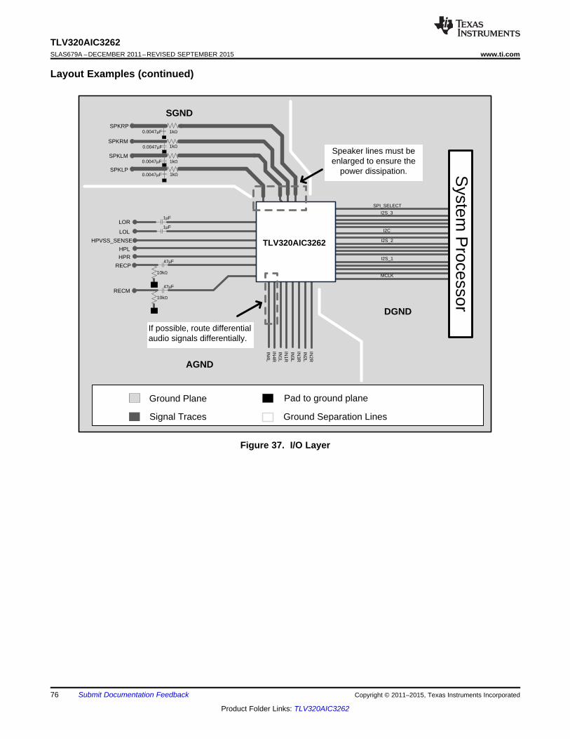
If possible, route differential audio signals differentially.
1kQ
1kQ
1kQ
1kQ0.0047µF
0.0047µF
0.0047µF
0.0047µF
SPKLP
SPKLM
SPKRM
SPKRP
1µF
1µFLOR
LOL
HPVSS_SENSE
HPLHPR
47µF
47µF
10kQ
10kQ
RECP
RECM
SPI_SELECT
I2S_3
I2C
I2S_2
I2S_1
MCLK
TLV320AIC3262
IN2R
IN2L
IN3R
IN3L
IN1R
IN1L
IN4R
IN4L
Speaker lines must be enlarged to ensure the
power dissipation.
Ground Plane
Ground Separation LinesSignal Traces
System
Processor
Pad to ground plane
AGND
SGND
DGND
TLV320AIC3262SLAS679A –DECEMBER 2011–REVISED SEPTEMBER 2015 www.ti.com
Layout Examples (continued)
Figure 37. I/O Layer
76 Submit Documentation Feedback Copyright © 2011–2015, Texas Instruments Incorporated
Product Folder Links: TLV320AIC3262

Decoupling capacitors for power supplies
should be placed close to the device terminals.
IOVDD
DVDD
DVDD
IOVDD
AV
DD
_18
VR
EF
_AU
DIO
VR
EF
_SA
RAVDD3_33
HVDD_18
SLVDD
SRVDD
10.1µF
10µF
10µF
10.1µF
47.1µF
2.2µF10.1µF
10.1µF
10.1µF
10.1µF
10.1µF
AV
DD
1_18
47.1µF
221Q
0.1µF10.1
µF
10.1µF
CPVDD_18AVDD4_18
AVDD2_18VNEG
RECVDD_33
(1)
(2)
(3)
(4)
(5)(6)
(7)
(1)
(2)
(3)
(4)
(5)
(6)
(7)
Minimal VIAS between the device terminals and
capacitor is recommended.
Place the filter capacitors on VREF_SAR,
VREF_AUDIO and VNEG near the device
for optimal performance.
10.1µF
1µF
TLV320AIC3262
AGND
SGND
DGND
Ground Plane
Ground Separation LinesSignal Traces
Pad to ground plane
TLV320AIC3262www.ti.com SLAS679A –DECEMBER 2011–REVISED SEPTEMBER 2015
Layout Examples (continued)
Figure 38. Power Layer
Copyright © 2011–2015, Texas Instruments Incorporated Submit Documentation Feedback 77
Product Folder Links: TLV320AIC3262

TLV320AIC3262SLAS679A –DECEMBER 2011–REVISED SEPTEMBER 2015 www.ti.com
14 Device and Documentation Support
14.1 Documentation Support
14.1.1 Related DocumentationFor related documentation, see the following:• TLV320AIC3262 Applications Reference Guide, SLAU309• TLV320AIC3262EVM User Guide, SLAU386
14.2 Community ResourcesThe following links connect to TI community resources. Linked contents are provided "AS IS" by the respectivecontributors. They do not constitute TI specifications and do not necessarily reflect TI's views; see TI's Terms ofUse.
TI E2E™ Online Community TI's Engineer-to-Engineer (E2E) Community. Created to foster collaborationamong engineers. At e2e.ti.com, you can ask questions, share knowledge, explore ideas and helpsolve problems with fellow engineers.
Design Support TI's Design Support Quickly find helpful E2E forums along with design support tools andcontact information for technical support.
14.3 TrademarksPowerTune, PurePath, E2E are trademarks of Texas Instruments.All other trademarks are the property of their respective owners.
14.4 Electrostatic Discharge CautionThese devices have limited built-in ESD protection. The leads should be shorted together or the device placed in conductive foamduring storage or handling to prevent electrostatic damage to the MOS gates.
14.5 GlossarySLYZ022 — TI Glossary.
This glossary lists and explains terms, acronyms, and definitions.
15 Mechanical, Packaging, and Orderable InformationThe following pages include mechanical, packaging, and orderable information. This information is the mostcurrent data available for the designated devices. This data is subject to change without notice and revision ofthis document. For browser-based versions of this data sheet, refer to the left-hand navigation.
78 Submit Documentation Feedback Copyright © 2011–2015, Texas Instruments Incorporated
Product Folder Links: TLV320AIC3262

PACKAGE OPTION ADDENDUM
www.ti.com 15-Apr-2017
Addendum-Page 1
PACKAGING INFORMATION
Orderable Device Status(1)
Package Type PackageDrawing
Pins PackageQty
Eco Plan(2)
Lead/Ball Finish(6)
MSL Peak Temp(3)
Op Temp (°C) Device Marking(4/5)
Samples
HPA02260IYZFR ACTIVE DSBGA YZF 81 2500 Green (RoHS& no Sb/Br)
SNAGCU Level-1-260C-UNLIM -40 to 85 AIC3262
TLV320AIC3262IYZFR ACTIVE DSBGA YZF 81 2500 Green (RoHS& no Sb/Br)
SNAGCU Level-1-260C-UNLIM -40 to 85 AIC3262
TLV320AIC3262IYZFT ACTIVE DSBGA YZF 81 250 Green (RoHS& no Sb/Br)
SNAGCU Level-1-260C-UNLIM -40 to 85 AIC3262
(1) The marketing status values are defined as follows:ACTIVE: Product device recommended for new designs.LIFEBUY: TI has announced that the device will be discontinued, and a lifetime-buy period is in effect.NRND: Not recommended for new designs. Device is in production to support existing customers, but TI does not recommend using this part in a new design.PREVIEW: Device has been announced but is not in production. Samples may or may not be available.OBSOLETE: TI has discontinued the production of the device.
(2) Eco Plan - The planned eco-friendly classification: Pb-Free (RoHS), Pb-Free (RoHS Exempt), or Green (RoHS & no Sb/Br) - please check http://www.ti.com/productcontent for the latest availabilityinformation and additional product content details.TBD: The Pb-Free/Green conversion plan has not been defined.Pb-Free (RoHS): TI's terms "Lead-Free" or "Pb-Free" mean semiconductor products that are compatible with the current RoHS requirements for all 6 substances, including the requirement thatlead not exceed 0.1% by weight in homogeneous materials. Where designed to be soldered at high temperatures, TI Pb-Free products are suitable for use in specified lead-free processes.Pb-Free (RoHS Exempt): This component has a RoHS exemption for either 1) lead-based flip-chip solder bumps used between the die and package, or 2) lead-based die adhesive used betweenthe die and leadframe. The component is otherwise considered Pb-Free (RoHS compatible) as defined above.Green (RoHS & no Sb/Br): TI defines "Green" to mean Pb-Free (RoHS compatible), and free of Bromine (Br) and Antimony (Sb) based flame retardants (Br or Sb do not exceed 0.1% by weightin homogeneous material)
(3) MSL, Peak Temp. - The Moisture Sensitivity Level rating according to the JEDEC industry standard classifications, and peak solder temperature.
(4) There may be additional marking, which relates to the logo, the lot trace code information, or the environmental category on the device.
(5) Multiple Device Markings will be inside parentheses. Only one Device Marking contained in parentheses and separated by a "~" will appear on a device. If a line is indented then it is a continuationof the previous line and the two combined represent the entire Device Marking for that device.
(6) Lead/Ball Finish - Orderable Devices may have multiple material finish options. Finish options are separated by a vertical ruled line. Lead/Ball Finish values may wrap to two lines if the finishvalue exceeds the maximum column width.
Important Information and Disclaimer:The information provided on this page represents TI's knowledge and belief as of the date that it is provided. TI bases its knowledge and belief on informationprovided by third parties, and makes no representation or warranty as to the accuracy of such information. Efforts are underway to better integrate information from third parties. TI has taken and

PACKAGE OPTION ADDENDUM
www.ti.com 15-Apr-2017
Addendum-Page 2
continues to take reasonable steps to provide representative and accurate information but may not have conducted destructive testing or chemical analysis on incoming materials and chemicals.TI and TI suppliers consider certain information to be proprietary, and thus CAS numbers and other limited information may not be available for release.
In no event shall TI's liability arising out of such information exceed the total purchase price of the TI part(s) at issue in this document sold by TI to Customer on an annual basis.

TAPE AND REEL INFORMATION
*All dimensions are nominal
Device PackageType
PackageDrawing
Pins SPQ ReelDiameter
(mm)
ReelWidth
W1 (mm)
A0(mm)
B0(mm)
K0(mm)
P1(mm)
W(mm)
Pin1Quadrant
TLV320AIC3262IYZFR DSBGA YZF 81 2500 330.0 12.4 5.04 5.07 0.75 8.0 12.0 Q1
TLV320AIC3262IYZFT DSBGA YZF 81 250 330.0 12.4 5.04 5.07 0.75 8.0 12.0 Q1
PACKAGE MATERIALS INFORMATION
www.ti.com 19-May-2018
Pack Materials-Page 1

*All dimensions are nominal
Device Package Type Package Drawing Pins SPQ Length (mm) Width (mm) Height (mm)
TLV320AIC3262IYZFR DSBGA YZF 81 2500 367.0 367.0 35.0
TLV320AIC3262IYZFT DSBGA YZF 81 250 367.0 367.0 35.0
PACKAGE MATERIALS INFORMATION
www.ti.com 19-May-2018
Pack Materials-Page 2

D: Max =
E: Max =
4.84 mm, Min =
4.84 mm, Min =
4.78 mm
4.78 mm

IMPORTANT NOTICE
Texas Instruments Incorporated (TI) reserves the right to make corrections, enhancements, improvements and other changes to itssemiconductor products and services per JESD46, latest issue, and to discontinue any product or service per JESD48, latest issue. Buyersshould obtain the latest relevant information before placing orders and should verify that such information is current and complete.TI’s published terms of sale for semiconductor products (http://www.ti.com/sc/docs/stdterms.htm) apply to the sale of packaged integratedcircuit products that TI has qualified and released to market. Additional terms may apply to the use or sale of other types of TI products andservices.Reproduction of significant portions of TI information in TI data sheets is permissible only if reproduction is without alteration and isaccompanied by all associated warranties, conditions, limitations, and notices. TI is not responsible or liable for such reproduceddocumentation. Information of third parties may be subject to additional restrictions. Resale of TI products or services with statementsdifferent from or beyond the parameters stated by TI for that product or service voids all express and any implied warranties for theassociated TI product or service and is an unfair and deceptive business practice. TI is not responsible or liable for any such statements.Buyers and others who are developing systems that incorporate TI products (collectively, “Designers”) understand and agree that Designersremain responsible for using their independent analysis, evaluation and judgment in designing their applications and that Designers havefull and exclusive responsibility to assure the safety of Designers' applications and compliance of their applications (and of all TI productsused in or for Designers’ applications) with all applicable regulations, laws and other applicable requirements. Designer represents that, withrespect to their applications, Designer has all the necessary expertise to create and implement safeguards that (1) anticipate dangerousconsequences of failures, (2) monitor failures and their consequences, and (3) lessen the likelihood of failures that might cause harm andtake appropriate actions. Designer agrees that prior to using or distributing any applications that include TI products, Designer willthoroughly test such applications and the functionality of such TI products as used in such applications.TI’s provision of technical, application or other design advice, quality characterization, reliability data or other services or information,including, but not limited to, reference designs and materials relating to evaluation modules, (collectively, “TI Resources”) are intended toassist designers who are developing applications that incorporate TI products; by downloading, accessing or using TI Resources in anyway, Designer (individually or, if Designer is acting on behalf of a company, Designer’s company) agrees to use any particular TI Resourcesolely for this purpose and subject to the terms of this Notice.TI’s provision of TI Resources does not expand or otherwise alter TI’s applicable published warranties or warranty disclaimers for TIproducts, and no additional obligations or liabilities arise from TI providing such TI Resources. TI reserves the right to make corrections,enhancements, improvements and other changes to its TI Resources. TI has not conducted any testing other than that specificallydescribed in the published documentation for a particular TI Resource.Designer is authorized to use, copy and modify any individual TI Resource only in connection with the development of applications thatinclude the TI product(s) identified in such TI Resource. NO OTHER LICENSE, EXPRESS OR IMPLIED, BY ESTOPPEL OR OTHERWISETO ANY OTHER TI INTELLECTUAL PROPERTY RIGHT, AND NO LICENSE TO ANY TECHNOLOGY OR INTELLECTUAL PROPERTYRIGHT OF TI OR ANY THIRD PARTY IS GRANTED HEREIN, including but not limited to any patent right, copyright, mask work right, orother intellectual property right relating to any combination, machine, or process in which TI products or services are used. Informationregarding or referencing third-party products or services does not constitute a license to use such products or services, or a warranty orendorsement thereof. Use of TI Resources may require a license from a third party under the patents or other intellectual property of thethird party, or a license from TI under the patents or other intellectual property of TI.TI RESOURCES ARE PROVIDED “AS IS” AND WITH ALL FAULTS. TI DISCLAIMS ALL OTHER WARRANTIES ORREPRESENTATIONS, EXPRESS OR IMPLIED, REGARDING RESOURCES OR USE THEREOF, INCLUDING BUT NOT LIMITED TOACCURACY OR COMPLETENESS, TITLE, ANY EPIDEMIC FAILURE WARRANTY AND ANY IMPLIED WARRANTIES OFMERCHANTABILITY, FITNESS FOR A PARTICULAR PURPOSE, AND NON-INFRINGEMENT OF ANY THIRD PARTY INTELLECTUALPROPERTY RIGHTS. TI SHALL NOT BE LIABLE FOR AND SHALL NOT DEFEND OR INDEMNIFY DESIGNER AGAINST ANY CLAIM,INCLUDING BUT NOT LIMITED TO ANY INFRINGEMENT CLAIM THAT RELATES TO OR IS BASED ON ANY COMBINATION OFPRODUCTS EVEN IF DESCRIBED IN TI RESOURCES OR OTHERWISE. IN NO EVENT SHALL TI BE LIABLE FOR ANY ACTUAL,DIRECT, SPECIAL, COLLATERAL, INDIRECT, PUNITIVE, INCIDENTAL, CONSEQUENTIAL OR EXEMPLARY DAMAGES INCONNECTION WITH OR ARISING OUT OF TI RESOURCES OR USE THEREOF, AND REGARDLESS OF WHETHER TI HAS BEENADVISED OF THE POSSIBILITY OF SUCH DAMAGES.Unless TI has explicitly designated an individual product as meeting the requirements of a particular industry standard (e.g., ISO/TS 16949and ISO 26262), TI is not responsible for any failure to meet such industry standard requirements.Where TI specifically promotes products as facilitating functional safety or as compliant with industry functional safety standards, suchproducts are intended to help enable customers to design and create their own applications that meet applicable functional safety standardsand requirements. Using products in an application does not by itself establish any safety features in the application. Designers mustensure compliance with safety-related requirements and standards applicable to their applications. Designer may not use any TI products inlife-critical medical equipment unless authorized officers of the parties have executed a special contract specifically governing such use.Life-critical medical equipment is medical equipment where failure of such equipment would cause serious bodily injury or death (e.g., lifesupport, pacemakers, defibrillators, heart pumps, neurostimulators, and implantables). Such equipment includes, without limitation, allmedical devices identified by the U.S. Food and Drug Administration as Class III devices and equivalent classifications outside the U.S.TI may expressly designate certain products as completing a particular qualification (e.g., Q100, Military Grade, or Enhanced Product).Designers agree that it has the necessary expertise to select the product with the appropriate qualification designation for their applicationsand that proper product selection is at Designers’ own risk. Designers are solely responsible for compliance with all legal and regulatoryrequirements in connection with such selection.Designer will fully indemnify TI and its representatives against any damages, costs, losses, and/or liabilities arising out of Designer’s non-compliance with the terms and provisions of this Notice.
Mailing Address: Texas Instruments, Post Office Box 655303, Dallas, Texas 75265Copyright © 2018, Texas Instruments Incorporated