slls115f –october 1980–revised september … · slls115f –october 1980–revised september...
TRANSCRIPT

4
12
2
13
6
75
10
911
14
1513
G
G
1A
1B
2A
2B
3A
3B
4A
4B
1Y
2Y
3Y
4Y
Copyright © 2016, Texas Instruments Incorporated
Product
Folder
Sample &Buy
Technical
Documents
Tools &
Software
Support &Community
An IMPORTANT NOTICE at the end of this data sheet addresses availability, warranty, changes, use in safety-critical applications,intellectual property matters and other important disclaimers. PRODUCTION DATA.
AM26LS32AC, AM26LS32AI, AM26LS32AMAM26LS33AC, AM26LS33AM
SLLS115F –OCTOBER 1980–REVISED SEPTEMBER 2016
AM26LS32Ax, AM26LS33Ax Quadruple Differential Line Receivers
1
1 Features1• AM26LS32A Devices Meet or Exceed the
Requirements of ANSI TIA/EIA-422-B, TIA/EIA-423-B, and ITU Recommendations V.10 and V.11
• AM26LS32A Devices Have ±7-V Common-ModeRange With ±200-mV Sensitivity
• AM26LS33A Devices Have ±15-V Common-ModeRange With ±500-mV Sensitivity
• Input Hysteresis 50 mV Typical• Operate From a Single 5-V Supply• Low-Power Schottky Circuitry• 3-State Outputs• Complementary Output-Enable Inputs• Input Impedance 12 kΩ Minimum• Open Input Fail-Safe
2 Applications• High-Reliability Automotive Applications• Factory Automation• ATM and Cash Counters• Smart Grids• AC and Servo Motor Drives
3 DescriptionThe AM26LS32Ax and AM26LS33Ax devices arequadruple differential line receivers for balanced andunbalanced digital data transmission. The enablefunction is common to all four receivers and offers achoice of active-high or active-low input. The 3-stateoutputs permit connection directly to a bus-organizedsystem. Fail-safe design ensures that, if the inputsare open, the outputs always are high.
Compared to the AM26LS32 and the AM26LS33, theAM26LS32A and AM26LS33A incorporate anadditional stage of amplification to improve sensitivity.The input impedance has been increased, resulting inless loading of the bus line. The additional stage hasincreased propagation delay; however, this does notaffect interchangeability in most applications.
The AM26LS32AC and AM26LS33AC arecharacterized for operation from 0°C to 70°C. TheAM26LS32AI is characterized for operation from–40°C to 85°C. The AM26LS32AM andAM26LS33AM are characterized for operation overthe full military temperature range of –55°C to 125°C.
Device Information(1)
PART NUMBER PACKAGE BODY SIZE (NOM)
AM26LS3xACAM26LS32AI
PDIP (16) 19.30 mm × 6.35 mmSOIC (16) 9.90 mm × 3.90 mm
AM26LS32ACSO (16) 10.20 mm × 5.30 mmTSSOP (16) 5.00 mm × 4.40 mm
AM26LS3xAMCDIP (16) 21.34 mm × 6.92 mmLCCC (20) 8.90 mm × 8.90 mm
(1) For all available packages, see the orderable addendum atthe end of the data sheet.
Logic Diagram (Positive Logic)
Pin numbers are for D, N, NS, or PW packages only.

2
AM26LS32AC, AM26LS32AI, AM26LS32AMAM26LS33AC, AM26LS33AMSLLS115F –OCTOBER 1980–REVISED SEPTEMBER 2016 www.ti.com
Product Folder Links: AM26LS32AC AM26LS32AM AM26LS33AM
Submit Documentation Feedback Copyright © 1980–2016, Texas Instruments Incorporated
Table of Contents1 Features .................................................................. 12 Applications ........................................................... 13 Description ............................................................. 14 Revision History..................................................... 25 Pin Configuration and Functions ......................... 36 Specifications......................................................... 4
6.1 Absolute Maximum Ratings ...................................... 46.2 ESD Ratings ............................................................ 46.3 Recommended Operating Conditions....................... 46.4 Thermal Information ................................................. 56.5 Electrical Characteristics........................................... 56.6 Switching Characteristics .......................................... 66.7 Dissipation Ratings ................................................... 66.8 Typical Characteristics .............................................. 7
7 Parameter Measurement Information .................. 98 Detailed Description ............................................ 11
8.1 Overview ................................................................. 118.2 Functional Block Diagram ....................................... 11
8.3 Feature Description................................................. 118.4 Device Functional Modes........................................ 11
9 Application and Implementation ........................ 129.1 Application Information .......................................... 129.2 Typical Application .................................................. 12
10 Power Supply Recommendations ..................... 1311 Layout................................................................... 13
11.1 Layout Guidelines ................................................. 1311.2 Layout Example .................................................... 14
12 Device and Documentation Support ................. 1512.1 Related Links ........................................................ 1512.2 Receiving Notification of Documentation Updates 1512.3 Community Resources.......................................... 1512.4 Trademarks ........................................................... 1512.5 Electrostatic Discharge Caution............................ 1512.6 Glossary ................................................................ 15
13 Mechanical, Packaging, and OrderableInformation ........................................................... 15
4 Revision HistoryNOTE: Page numbers for previous revisions may differ from page numbers in the current version.
Changes from Revision E (October 2007) to Revision F Page
• Added Applications section, ESD Ratings table, Feature Description section, Device Functional Modes, Applicationand Implementation section, Power Supply Recommendations section, Layout section, Device and DocumentationSupport section, and Mechanical, Packaging, and Orderable Information section................................................................ 1
• Changed RθJA values in the Thermal Information table: 73 to 75.7 for (D), 67 to 45.3 (N), 64 to 75.8 (NS), and 108 to102.7 (PW).............................................................................................................................................................................. 5

41Y
5G
6NC
72Y
82A
92B
10G
ND
11N
C
123B
133A
14 3Y
15 G
16 NC
17 4Y
18 4A
194B
20V
CC
1N
C
21B
31A
Not to scale
11B 16 VCC
21A 15 4B
31Y 14 4A
4G 13 4Y
52Y 12 G
62A 11 3Y
72B 10 3A
8GND 9 3B
Not to scale
3
AM26LS32AC, AM26LS32AI, AM26LS32AMAM26LS33AC, AM26LS33AM
www.ti.com SLLS115F –OCTOBER 1980–REVISED SEPTEMBER 2016
Product Folder Links: AM26LS32AC AM26LS32AM AM26LS33AM
Submit Documentation FeedbackCopyright © 1980–2016, Texas Instruments Incorporated
5 Pin Configuration and Functions
D, J, N, NS, and PW Package16-Pin SOIC, CDIP, PDIP, SO, and TSSOP
Top ViewFK Package20-Pin LCCC
Top View
NC - No internal connection
Pin FunctionsPIN
I/O DESCRIPTIONNAME SOIC, CDIP, PDIP,
SO, TSSOP LCCC
1A 2 3 I RS422/RS485 differential input (noninverting)1B 1 2 I RS422/RS485 differential input (inverting)1Y 3 4 O Logic level output2A 6 8 I RS422/RS485 differential input (noninverting)2B 7 9 I RS422/RS485 differential input (inverting)2Y 5 7 O Logic level output3A 10 13 I RS422/RS485 differential input (noninverting)3B 9 12 I RS422/RS485 differential input (inverting)3Y 11 14 O Logic level output4A 14 18 I RS422/RS485 differential input (noninverting)4B 15 19 I RS422/RS485 differential input (inverting)4Y 13 17 O Logic level outputG 12 15 I Active-Low selectG 4 5 I Active-High selectGND 8 10 — GroundNC — 1, 6, 11, 16 — No internal connectionVCC 16 20 — Power supply

4
AM26LS32AC, AM26LS32AI, AM26LS32AMAM26LS33AC, AM26LS33AMSLLS115F –OCTOBER 1980–REVISED SEPTEMBER 2016 www.ti.com
Product Folder Links: AM26LS32AC AM26LS32AM AM26LS33AM
Submit Documentation Feedback Copyright © 1980–2016, Texas Instruments Incorporated
(1) Stresses beyond those listed under Absolute Maximum Ratings may cause permanent damage to the device. These are stress ratingsonly, which do not imply functional operation of the device at these or any other conditions beyond those indicated under RecommendedOperating Conditions. Exposure to absolute-maximum-rated conditions for extended periods may affect device reliability.
(2) All voltage values, except differential voltages, are with respect to the network ground terminal.(3) Differential voltage values are at the noninverting (A) input terminals with respect to the inverting (B) input terminals.(4) 1.6 mm (1/16 inch) from case
6 Specifications
6.1 Absolute Maximum Ratingsover operating free-air temperature range (unless otherwise noted) (1)
MIN MAX UNITSupply voltage, VCC
(2) 7 V
Input voltage, VIAny differential input ±25
VOther inputs 7
Differential input voltage, VID(3) ±25 V
Continuous total power dissipation See Dissipation RatingsCase temperature, TC, FK package (60 s) 260 °C
Lead temperature (4) D or N package (10 s) 260°C
J package (60 s) 300Storage temperature, Tstg –65 150 °C
(1) JEDEC document JEP155 states that 500-V HBM allows safe manufacturing with a standard ESD control process.(2) JEDEC document JEP157 states that 250-V CDM allows safe manufacturing with a standard ESD control process.
6.2 ESD RatingsVALUE UNIT
V(ESD) Electrostatic dischargeHuman-body model (HBM), per ANSI/ESDA/JEDEC JS-001 (1) ±500
VCharged-device model (CDM), per JEDEC specification JESD22-C101 (2) ±2000
6.3 Recommended Operating ConditionsMIN NOM MAX UNIT
VCC Supply voltageAM26LS32AC, AM26LS32AI, AM26LS33AC 4.75 5 5.25
VAM26LS32AM, AM26LS33AM 4.5 5 5.5
VIH High-level input voltage 2 VVIL Low-level input voltage 0.8 V
VIC Common-mode input voltageAM26LS32A ±7
VAM26LS33A ±15
IOH High-level output current –440 µAIOL Low-level output current 8 mA
TA Operating free-air temperatureAM26LS32AC, AM26LS33AC 0 70
°CAM26LS32AI –40 85AM26LS32AM, AM26LS33AM –55 125
5
AM26LS32AC, AM26LS32AI, AM26LS32AMAM26LS33AC, AM26LS33AM
www.ti.com SLLS115F –OCTOBER 1980–REVISED SEPTEMBER 2016
Product Folder Links: AM26LS32AC AM26LS32AM AM26LS33AM
Submit Documentation FeedbackCopyright © 1980–2016, Texas Instruments Incorporated
(1) For more information about traditional and new thermal metrics, see the Semiconductor and IC Package Thermal Metrics applicationreport.
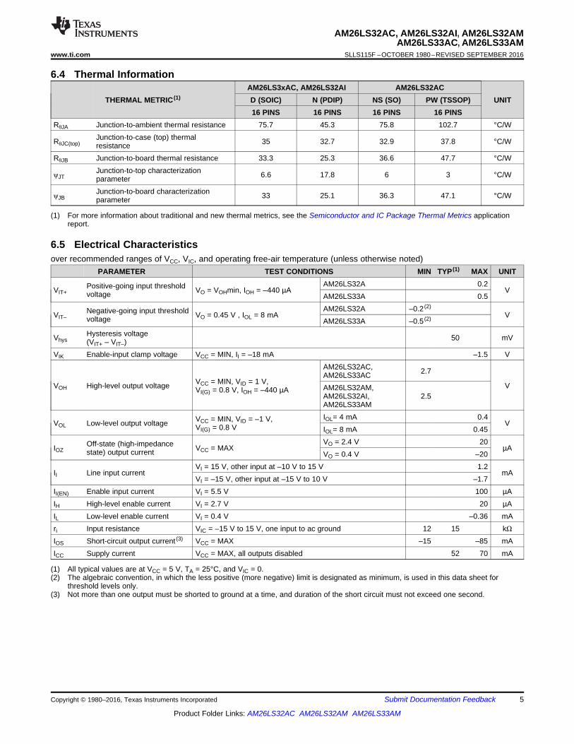
6.4 Thermal Information
THERMAL METRIC (1)AM26LS3xAC, AM26LS32AI AM26LS32AC
UNITD (SOIC) N (PDIP) NS (SO) PW (TSSOP)16 PINS 16 PINS 16 PINS 16 PINS
RθJA Junction-to-ambient thermal resistance 75.7 45.3 75.8 102.7 °C/W
RθJC(top)Junction-to-case (top) thermalresistance 35 32.7 32.9 37.8 °C/W
RθJB Junction-to-board thermal resistance 33.3 25.3 36.6 47.7 °C/W
ψJTJunction-to-top characterizationparameter 6.6 17.8 6 3 °C/W
ψJBJunction-to-board characterizationparameter 33 25.1 36.3 47.1 °C/W
(1) All typical values are at VCC = 5 V, TA = 25°C, and VIC = 0.(2) The algebraic convention, in which the less positive (more negative) limit is designated as minimum, is used in this data sheet for
threshold levels only.(3) Not more than one output must be shorted to ground at a time, and duration of the short circuit must not exceed one second.
6.5 Electrical Characteristicsover recommended ranges of VCC, VIC, and operating free-air temperature (unless otherwise noted)
PARAMETER TEST CONDITIONS MIN TYP (1) MAX UNIT
VIT+Positive-going input thresholdvoltage VO = VOHmin, IOH = –440 µA
AM26LS32A 0.2V
AM26LS33A 0.5
VIT–Negative-going input thresholdvoltage VO = 0.45 V , IOL = 8 mA
AM26LS32A –0.2 (2)V
AM26LS33A –0.5 (2)
VhysHysteresis voltage(VIT+ – VIT–) 50 mV
VIK Enable-input clamp voltage VCC = MIN, II = –18 mA –1.5 V
VOH High-level output voltage VCC = MIN, VID = 1 V,VI(G) = 0.8 V, IOH = –440 µA
AM26LS32AC,AM26LS33AC 2.7
VAM26LS32AM,AM26LS32AI,AM26LS33AM
2.5
VOL Low-level output voltage VCC = MIN, VID = –1 V,VI(G) = 0.8 V
IOL= 4 mA 0.4V
IOL= 8 mA 0.45
IOZOff-state (high-impedancestate) output current VCC = MAX
VO = 2.4 V 20µA
VO = 0.4 V –20
II Line input currentVI = 15 V, other input at –10 V to 15 V 1.2
mAVI = –15 V, other input at –15 V to 10 V –1.7
II(EN) Enable input current VI = 5.5 V 100 µAIH High-level enable current VI = 2.7 V 20 µAIL Low-level enable current VI = 0.4 V –0.36 mAri Input resistance VIC = –15 V to 15 V, one input to ac ground 12 15 kΩIOS Short-circuit output current (3) VCC = MAX –15 –85 mAICC Supply current VCC = MAX, all outputs disabled 52 70 mA

6
AM26LS32AC, AM26LS32AI, AM26LS32AMAM26LS33AC, AM26LS33AMSLLS115F –OCTOBER 1980–REVISED SEPTEMBER 2016 www.ti.com
Product Folder Links: AM26LS32AC AM26LS32AM AM26LS33AM
Submit Documentation Feedback Copyright © 1980–2016, Texas Instruments Incorporated
(1) All typical values are at VCC = 5 V, TA = 25°C, and VIC = 0.
6.6 Switching CharacteristicsCL = 15 pF, VCC = 5 V, and TA = 25°C (see Parameter Measurement Information; unless otherwise noted)
PARAMETER MIN TYP (1) MAX UNITtPLH Propagation delay time, low-to-high-level output 20 35 nstPHL Propagation delay time, high-to-low-level output 22 35 nstPZH Output enable time to high level 17 22 nstPZL Output enable time to low level 20 25 nstPHZ Output disable time from high level 21 30 nstPLZ Output disable time from low level 30 40 ns
6.7 Dissipation RatingsPACKAGE TA ≤ 25°C
POWER RATINGDERATION FACTOR
ABOVE TA = 25°CTA = 70°C
POWER RATINGTA = 125°C
POWER RATINGFK 1375 mW 11 mW/°C 880 mW 275 mWJ 1375 mW 11 mW/°C 880 mW 275 mW

Ou
tpu
t V
olt
ag
e,
V(V
)O
Enable G Voltage (V)
Load = 8 k to GNDΩ
Ou
tpu
t V
olt
ag
e,
V(V
)O
Enable G Voltage (V)
Load = 1 k toΩ VCC
Lo
w-L
ev
el
Ou
tpu
t V
otl
ag
e,
V(
)O
LV
Free-Air Temperature, T ( C)A °
Load = 8 k to GNDΩ
Enable G Voltage (V)
Ou
tpu
t V
olt
ag
e,
V(V
)O
High-Level Output Current, I (mA)OH
Hig
h-L
ev
el
Ou
tpu
t V
olt
ag
e,
V(V
)O
H
Low-Level Output Current, I (mA)OL
Lo
w-L
evel O
utp
ut
Vo
ltag
e, V
(V)
OL
7
AM26LS32AC, AM26LS32AI, AM26LS32AMAM26LS33AC, AM26LS33AM
www.ti.com SLLS115F –OCTOBER 1980–REVISED SEPTEMBER 2016
Product Folder Links: AM26LS32AC AM26LS32AM AM26LS33AM
Submit Documentation FeedbackCopyright © 1980–2016, Texas Instruments Incorporated
6.8 Typical Characteristics
Figure 1. High-Level Output Voltagevs High-Level Output Current
Figure 2. Low-Level Output Voltagevs Low-Level Output Current
Figure 3. Low-Level Output Voltage vs Free-Air Temperature Figure 4. Output Voltage vs Enable G Voltage
Figure 5. Output Voltage vs Enable G Voltage Figure 6. Output Voltage vs Enable G Voltage
Input Voltage, V (V)I
Inp
ut
Cu
rre
nt,
I(m
A)
I
Ou
tpu
t V
olt
ag
e,
V(V
)O
Differential Input Voltage, V (mV)ID
Load = 1 k toΩ VCC
Ou
tpu
t V
olt
ag
e,
V(V
)O
Enable G Voltage (V) Differential Input Voltage, V (mV)ID
Ou
tpu
t V
olt
ag
e,
V(V
)O
8
AM26LS32AC, AM26LS32AI, AM26LS32AMAM26LS33AC, AM26LS33AMSLLS115F –OCTOBER 1980–REVISED SEPTEMBER 2016 www.ti.com
Product Folder Links: AM26LS32AC AM26LS32AM AM26LS33AM
Submit Documentation Feedback Copyright © 1980–2016, Texas Instruments Incorporated
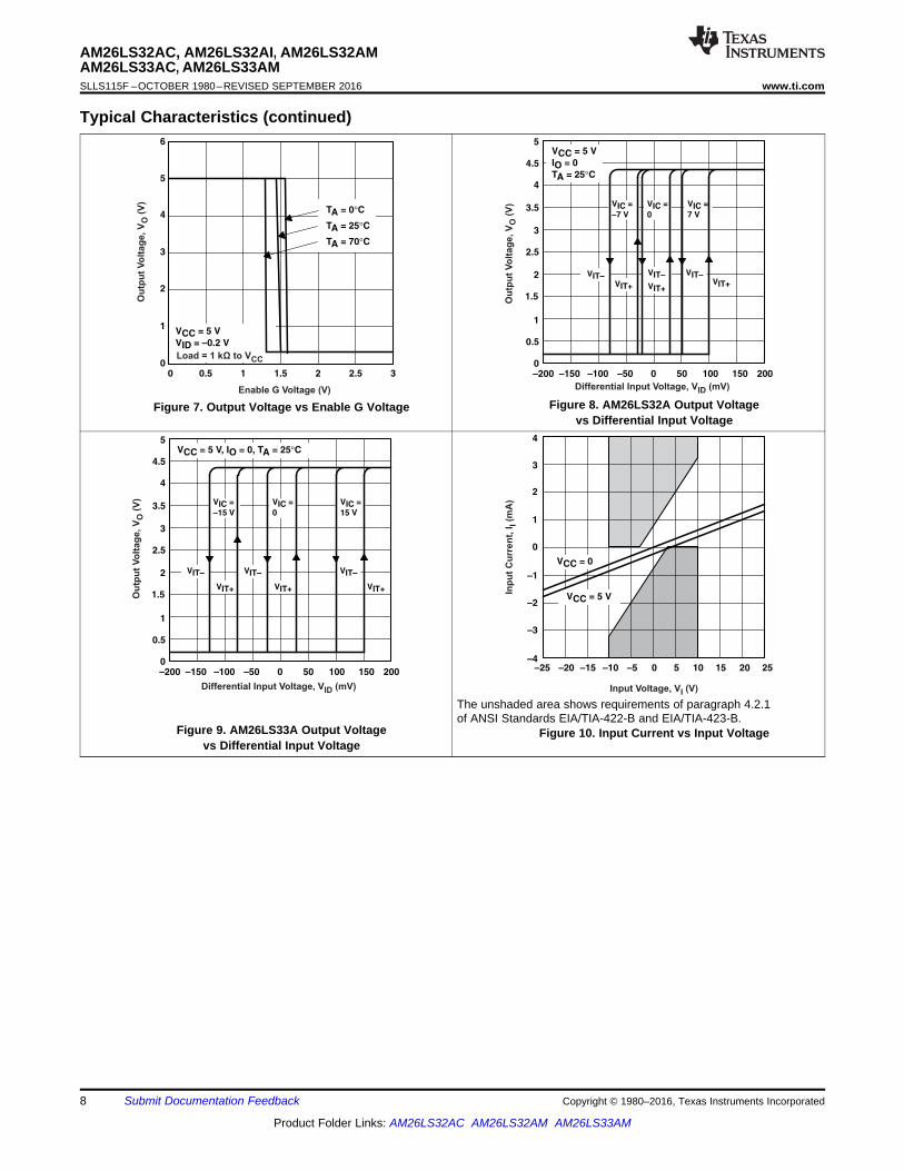
Typical Characteristics (continued)
Figure 7. Output Voltage vs Enable G Voltage Figure 8. AM26LS32A Output Voltagevs Differential Input Voltage
Figure 9. AM26LS33A Output Voltagevs Differential Input Voltage
The unshaded area shows requirements of paragraph 4.2.1of ANSI Standards EIA/TIA-422-B and EIA/TIA-423-B.
Figure 10. Input Current vs Input Voltage

S1 Open
S2 Closed
10%
90%
10%
90%
0
3 V
10%10%
90% 90%
1.3 V1.3 V
1.3 V 1.3 V
3 V
0
≤5 ns
Enable G
Enable G
tPZH
1.3 VOutputVOH
0.5 V
≈1.4 V
tPHZ S1 Closed
S2 Closed
See Note C
≤5 ns
tPHL
VOH
VOL
2.5 V
–2.5 V
tPLH
S1 and S2 Closed
Input
Output
00
1.3 V 1.3 V
5 kΩ
S1
RL = 2 kΩ
VCC
From Output
Under Test
CL(see Note A) See Note B
S2
Test
Point
9
AM26LS32AC, AM26LS32AI, AM26LS32AMAM26LS33AC, AM26LS33AM
www.ti.com SLLS115F –OCTOBER 1980–REVISED SEPTEMBER 2016
Product Folder Links: AM26LS32AC AM26LS32AM AM26LS33AM
Submit Documentation FeedbackCopyright © 1980–2016, Texas Instruments Incorporated
7 Parameter Measurement Information
Figure 11. Test Circuit
Figure 12. Voltage Waveforms For tPLH, tPHL
Figure 13. Voltage Waveforms For tPHZ, tPZH

100 kΩ
100 kΩ
8.3 kΩ85 Ω
20 kΩ960 Ω
960 Ω
Copyright © 2016, Texas Instruments Incorporated
10%
90%
10%
90%
0
3 V
10%10%
90% 90%
1.3 V1.3 V
1.3 V 1.3 V
3 V
0
tPZL
1.3 V
S1 Closed
S2 Open
S1 ClosedS2 Closed
VOL0.5 V
tPLZOutput
Enable G
Enable G
≤5 ns ≤5 ns
≈1.4 V
10
AM26LS32AC, AM26LS32AI, AM26LS32AMAM26LS33AC, AM26LS33AMSLLS115F –OCTOBER 1980–REVISED SEPTEMBER 2016 www.ti.com
Product Folder Links: AM26LS32AC AM26LS32AM AM26LS33AM
Submit Documentation Feedback Copyright © 1980–2016, Texas Instruments Incorporated
Parameter Measurement Information (continued)
A. CL includes probe and jig capacitance.B. All diodes are 1N3064 or equivalent.C. Enable G is tested with G high, G is tested with G low.
Figure 14. Voltage Waveforms For tPLZ, tPZL
Figure 15. Schematics of Inputs and Outputs
4
12
2
13
6
75
10
911
14
1513
G
G
1A
1B
2A
2B
3A
3B
4A
4B
1Y
2Y
3Y
4Y
Copyright © 2016, Texas Instruments Incorporated
11
AM26LS32AC, AM26LS32AI, AM26LS32AMAM26LS33AC, AM26LS33AM
www.ti.com SLLS115F –OCTOBER 1980–REVISED SEPTEMBER 2016
Product Folder Links: AM26LS32AC AM26LS32AM AM26LS33AM
Submit Documentation FeedbackCopyright © 1980–2016, Texas Instruments Incorporated
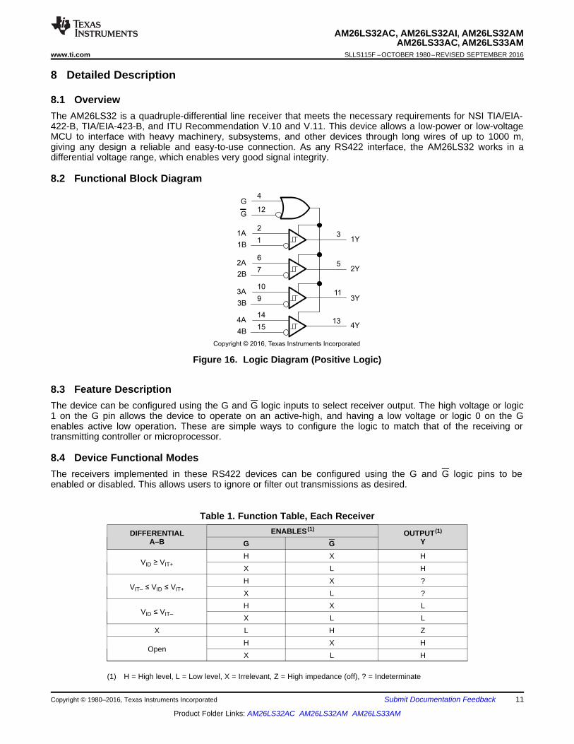
8 Detailed Description
8.1 OverviewThe AM26LS32 is a quadruple-differential line receiver that meets the necessary requirements for NSI TIA/EIA-422-B, TIA/EIA-423-B, and ITU Recommendation V.10 and V.11. This device allows a low-power or low-voltageMCU to interface with heavy machinery, subsystems, and other devices through long wires of up to 1000 m,giving any design a reliable and easy-to-use connection. As any RS422 interface, the AM26LS32 works in adifferential voltage range, which enables very good signal integrity.
8.2 Functional Block Diagram
Figure 16. Logic Diagram (Positive Logic)
8.3 Feature DescriptionThe device can be configured using the G and G logic inputs to select receiver output. The high voltage or logic1 on the G pin allows the device to operate on an active-high, and having a low voltage or logic 0 on the Genables active low operation. These are simple ways to configure the logic to match that of the receiving ortransmitting controller or microprocessor.
8.4 Device Functional ModesThe receivers implemented in these RS422 devices can be configured using the G and G logic pins to beenabled or disabled. This allows users to ignore or filter out transmissions as desired.
(1) H = High level, L = Low level, X = Irrelevant, Z = High impedance (off), ? = Indeterminate
Table 1. Function Table, Each Receiver
DIFFERENTIALA–B
ENABLES (1) OUTPUT (1)
YG G
VID ≥ VIT+H X HX L H
VIT– ≤ VID ≤ VIT+H X ?X L ?
VID ≤ VIT–H X LX L L
X L H Z
OpenH X HX L H

Copyright © 2016, Texas Instruments Incorporated
12
AM26LS32AC, AM26LS32AI, AM26LS32AMAM26LS33AC, AM26LS33AMSLLS115F –OCTOBER 1980–REVISED SEPTEMBER 2016 www.ti.com
Product Folder Links: AM26LS32AC AM26LS32AM AM26LS33AM
Submit Documentation Feedback Copyright © 1980–2016, Texas Instruments Incorporated
9 Application and Implementation
NOTEInformation in the following applications sections is not part of the TI componentspecification, and TI does not warrant its accuracy or completeness. TI’s customers areresponsible for determining suitability of components for their purposes. Customers shouldvalidate and test their design implementation to confirm system functionality.
9.1 Application InformationWhen using AM26LS32A as a receiver, the AM26LS31AC can allow multiple AM26LS32As to be used causingan increase in the amount of outputs.
9.2 Typical ApplicationFigure 17 shows a configuration with no termination. Although reflections are present at the receiver inputs at adata signaling rate of 200 kbps with no termination, the RS-422-compliant receiver reads only the inputdifferential voltage and produces a clean signal at the output.
†RT equals the characteristic impedance of the line.
Figure 17. Application Diagram
9.2.1 Design RequirementsResistor and capacitor (if used) termination values are shown for each laboratory experiment, but vary fromsystem to system. For example, the termination resistor, RT, must be within 20% of the characteristic impedance,ZO, of the cable and can vary from about 80 Ω to 120 Ω.
9.2.2 Detailed Design ProcedureAdd a VCC bypass capacitor (0.1 µF or more). Either enable (G pin) input can turn on the receivers, so connectthe desired enable to a compatible logic line output. The other enable input must be tied to the inactive statesupply rail. If the receivers must always be active, then connect both enables to the supply rail such that at leastone is set to an active-state rail. VCC must be 5 V within 10% and logic inputs must provide TTL-compatiblevoltage levels A & B Inputs can lead to an external connector or can be left unconnected. The last receiver on acable requires termination, either on-board or use as an external resistor. Unused Y outputs can be leftunconnected.
Free-Air Temperature, T (A °C)
Hig
h-L
evel O
utp
ut
Vo
ltag
e, V
(O
HV
) I = 440 AOH – μ
13
AM26LS32AC, AM26LS32AI, AM26LS32AMAM26LS33AC, AM26LS33AM
www.ti.com SLLS115F –OCTOBER 1980–REVISED SEPTEMBER 2016
Product Folder Links: AM26LS32AC AM26LS32AM AM26LS33AM
Submit Documentation FeedbackCopyright © 1980–2016, Texas Instruments Incorporated
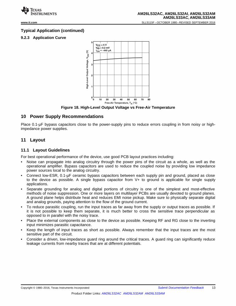
Typical Application (continued)9.2.3 Application Curve
Figure 18. High-Level Output Voltage vs Free-Air Temperature
10 Power Supply RecommendationsPlace 0.1-µF bypass capacitors close to the power-supply pins to reduce errors coupling in from noisy or high-impedance power supplies.
11 Layout
11.1 Layout GuidelinesFor best operational performance of the device, use good PCB layout practices including:• Noise can propagate into analog circuitry through the power pins of the circuit as a whole, as well as the
operational amplifier. Bypass capacitors are used to reduce the coupled noise by providing low impedancepower sources local to the analog circuitry.
• Connect low-ESR, 0.1-µF ceramic bypass capacitors between each supply pin and ground, placed as closeto the device as possible. A single bypass capacitor from V+ to ground is applicable for single supplyapplications.
• Separate grounding for analog and digital portions of circuitry is one of the simplest and most-effectivemethods of noise suppression. One or more layers on multilayer PCBs are usually devoted to ground planes.A ground plane helps distribute heat and reduces EMI noise pickup. Make sure to physically separate digitaland analog grounds, paying attention to the flow of the ground current.
• To reduce parasitic coupling, run the input traces as far away from the supply or output traces as possible. Ifit is not possible to keep them separate, it is much better to cross the sensitive trace perpendicular asopposed to in parallel with the noisy trace.
• Place the external components as close to the device as possible. Keeping RF and RG close to the invertinginput minimizes parasitic capacitance.
• Keep the length of input traces as short as possible. Always remember that the input traces are the mostsensitive part of the circuit.
• Consider a driven, low-impedance guard ring around the critical traces. A guard ring can significantly reduceleakage currents from nearby traces that are at different potentials.

VCC
0.1 F
VDD
1
2
3
4
5
6
7
8
16
15
14
13
12
11
10
9
Reduce logic signal trace when possible
4B
4A
4Y
G
3Y
3A
3B
2B
2A
2Y
G
1Y
1A
1B
Termination Resistor
14
AM26LS32AC, AM26LS32AI, AM26LS32AMAM26LS33AC, AM26LS33AMSLLS115F –OCTOBER 1980–REVISED SEPTEMBER 2016 www.ti.com
Product Folder Links: AM26LS32AC AM26LS32AM AM26LS33AM
Submit Documentation Feedback Copyright © 1980–2016, Texas Instruments Incorporated
11.2 Layout Example
Figure 19. Layout with PCB Recommendations

15
AM26LS32AC, AM26LS32AI, AM26LS32AMAM26LS33AC, AM26LS33AM
www.ti.com SLLS115F –OCTOBER 1980–REVISED SEPTEMBER 2016
Product Folder Links: AM26LS32AC AM26LS32AM AM26LS33AM
Submit Documentation FeedbackCopyright © 1980–2016, Texas Instruments Incorporated
12 Device and Documentation Support
12.1 Related LinksThe table below lists quick access links. Categories include technical documents, support and communityresources, tools and software, and quick access to sample or buy.
Table 2. Related Links
PARTS PRODUCT FOLDER SAMPLE & BUY TECHNICALDOCUMENTS
TOOLS &SOFTWARE
SUPPORT &COMMUNITY
AM26LS32AC Click here Click here Click here Click here Click hereAM26LS32AI Click here Click here Click here Click here Click hereAM26LS32AM Click here Click here Click here Click here Click hereAM26LS33AC Click here Click here Click here Click here Click hereAM26LS33AM Click here Click here Click here Click here Click here
12.2 Receiving Notification of Documentation UpdatesTo receive notification of documentation updates, navigate to the device product folder on ti.com. In the upperright corner, click on Alert me to register and receive a weekly digest of any product information that haschanged. For change details, review the revision history included in any revised document.
12.3 Community ResourcesThe following links connect to TI community resources. Linked contents are provided "AS IS" by the respectivecontributors. They do not constitute TI specifications and do not necessarily reflect TI's views; see TI's Terms ofUse.
TI E2E™ Online Community TI's Engineer-to-Engineer (E2E) Community. Created to foster collaborationamong engineers. At e2e.ti.com, you can ask questions, share knowledge, explore ideas and helpsolve problems with fellow engineers.
Design Support TI's Design Support Quickly find helpful E2E forums along with design support tools andcontact information for technical support.
12.4 TrademarksE2E is a trademark of Texas Instruments.All other trademarks are the property of their respective owners.
12.5 Electrostatic Discharge CautionThese devices have limited built-in ESD protection. The leads should be shorted together or the device placed in conductive foamduring storage or handling to prevent electrostatic damage to the MOS gates.
12.6 GlossarySLYZ022 — TI Glossary.
This glossary lists and explains terms, acronyms, and definitions.
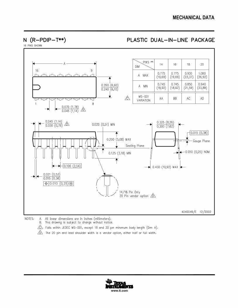
13 Mechanical, Packaging, and Orderable InformationThe following pages include mechanical, packaging, and orderable information. This information is the mostcurrent data available for the designated devices. This data is subject to change without notice and revision ofthis document. For browser-based versions of this data sheet, refer to the left-hand navigation.

PACKAGE OPTION ADDENDUM
www.ti.com 25-Oct-2016
Addendum-Page 1
PACKAGING INFORMATION
Orderable Device Status(1)
Package Type PackageDrawing
Pins PackageQty
Eco Plan(2)
Lead/Ball Finish(6)
MSL Peak Temp(3)
Op Temp (°C) Device Marking(4/5)
Samples
5962-7802003M2A ACTIVE LCCC FK 20 1 TBD POST-PLATE N / A for Pkg Type -55 to 125 5962-7802003M2AAM26LS32AMFKB
5962-7802003MEA ACTIVE CDIP J 16 1 TBD A42 N / A for Pkg Type -55 to 125 5962-7802003MEAAM26LS32AMJB
5962-7802003MFA ACTIVE CFP W 16 1 TBD A42 N / A for Pkg Type -55 to 125 5962-7802003MFAAM26LS32AMWB
5962-7802004M2A ACTIVE LCCC FK 20 1 TBD POST-PLATE N / A for Pkg Type -55 to 125 5962-7802004M2AAM26LS33AMFKB
5962-7802004MEA ACTIVE CDIP J 16 1 TBD A42 N / A for Pkg Type -55 to 125 5962-7802004MEAAM26LS33AMJB
5962-7802004MFA ACTIVE CFP W 16 1 TBD A42 N / A for Pkg Type -55 to 125 5962-7802004MFAAM26LS33AMWB
AM26LS32ACD ACTIVE SOIC D 16 40 Green (RoHS& no Sb/Br)
CU NIPDAU Level-1-260C-UNLIM 0 to 70 26LS32AC
AM26LS32ACDE4 ACTIVE SOIC D 16 40 Green (RoHS& no Sb/Br)
CU NIPDAU Level-1-260C-UNLIM 0 to 70 26LS32AC
AM26LS32ACDG4 ACTIVE SOIC D 16 40 Green (RoHS& no Sb/Br)
CU NIPDAU Level-1-260C-UNLIM 0 to 70 26LS32AC
AM26LS32ACDR ACTIVE SOIC D 16 2500 Green (RoHS& no Sb/Br)
CU NIPDAU Level-1-260C-UNLIM 0 to 70 26LS32AC
AM26LS32ACDRE4 ACTIVE SOIC D 16 2500 Green (RoHS& no Sb/Br)
CU NIPDAU Level-1-260C-UNLIM 0 to 70 26LS32AC
AM26LS32ACDRG4 ACTIVE SOIC D 16 2500 Green (RoHS& no Sb/Br)
CU NIPDAU Level-1-260C-UNLIM 0 to 70 26LS32AC
AM26LS32ACN ACTIVE PDIP N 16 25 Pb-Free(RoHS)
CU NIPDAU N / A for Pkg Type 0 to 70 AM26LS32ACN

PACKAGE OPTION ADDENDUM
www.ti.com 25-Oct-2016
Addendum-Page 2
Orderable Device Status(1)
Package Type PackageDrawing
Pins PackageQty
Eco Plan(2)
Lead/Ball Finish(6)
MSL Peak Temp(3)
Op Temp (°C) Device Marking(4/5)
Samples
AM26LS32ACNE4 ACTIVE PDIP N 16 25 Pb-Free(RoHS)
CU NIPDAU N / A for Pkg Type 0 to 70 AM26LS32ACN
AM26LS32ACNSR ACTIVE SO NS 16 2000 Green (RoHS& no Sb/Br)
CU NIPDAU Level-1-260C-UNLIM 0 to 70 26LS32A
AM26LS32ACNSRG4 ACTIVE SO NS 16 2000 Green (RoHS& no Sb/Br)
CU NIPDAU Level-1-260C-UNLIM 0 to 70 26LS32A
AM26LS32ACPW ACTIVE TSSOP PW 16 90 Green (RoHS& no Sb/Br)
CU NIPDAU Level-1-260C-UNLIM 0 to 70 SA32A
AM26LS32ACPWE4 ACTIVE TSSOP PW 16 90 Green (RoHS& no Sb/Br)
CU NIPDAU Level-1-260C-UNLIM 0 to 70 SA32A
AM26LS32ACPWR ACTIVE TSSOP PW 16 2000 Green (RoHS& no Sb/Br)
CU NIPDAU Level-1-260C-UNLIM 0 to 70 SA32A
AM26LS32ACPWRE4 ACTIVE TSSOP PW 16 2000 Green (RoHS& no Sb/Br)
CU NIPDAU Level-1-260C-UNLIM 0 to 70 SA32A
AM26LS32ACPWRG4 ACTIVE TSSOP PW 16 2000 Green (RoHS& no Sb/Br)
CU NIPDAU Level-1-260C-UNLIM 0 to 70 SA32A
AM26LS32AID ACTIVE SOIC D 16 40 Green (RoHS& no Sb/Br)
CU NIPDAU Level-1-260C-UNLIM -40 to 85 26LS32AI
AM26LS32AIDE4 ACTIVE SOIC D 16 40 Green (RoHS& no Sb/Br)
CU NIPDAU Level-1-260C-UNLIM -40 to 85 26LS32AI
AM26LS32AIDG4 ACTIVE SOIC D 16 40 Green (RoHS& no Sb/Br)
CU NIPDAU Level-1-260C-UNLIM -40 to 85 26LS32AI
AM26LS32AIDR ACTIVE SOIC D 16 2500 Green (RoHS& no Sb/Br)
CU NIPDAU Level-1-260C-UNLIM -40 to 85 26LS32AI
AM26LS32AIDRG4 ACTIVE SOIC D 16 2500 Green (RoHS& no Sb/Br)
CU NIPDAU Level-1-260C-UNLIM -40 to 85 26LS32AI
AM26LS32AIN ACTIVE PDIP N 16 25 Pb-Free(RoHS)
CU NIPDAU N / A for Pkg Type -40 to 85 AM26LS32AIN
AM26LS32AINE4 ACTIVE PDIP N 16 25 Pb-Free(RoHS)
CU NIPDAU N / A for Pkg Type -40 to 85 AM26LS32AIN
AM26LS32AMFKB ACTIVE LCCC FK 20 1 TBD POST-PLATE N / A for Pkg Type -55 to 125 5962-7802003M2AAM26LS32AMFKB
AM26LS32AMJ ACTIVE CDIP J 16 1 TBD A42 N / A for Pkg Type -55 to 125 AM26LS32AMJ

PACKAGE OPTION ADDENDUM
www.ti.com 25-Oct-2016
Addendum-Page 3
Orderable Device Status(1)
Package Type PackageDrawing
Pins PackageQty
Eco Plan(2)
Lead/Ball Finish(6)
MSL Peak Temp(3)
Op Temp (°C) Device Marking(4/5)
Samples
AM26LS32AMJB ACTIVE CDIP J 16 1 TBD A42 N / A for Pkg Type -55 to 125 5962-7802003MEAAM26LS32AMJB
AM26LS32AMWB ACTIVE CFP W 16 1 TBD A42 N / A for Pkg Type -55 to 125 5962-7802003MFAAM26LS32AMWB
AM26LS33ACD ACTIVE SOIC D 16 40 Green (RoHS& no Sb/Br)
CU NIPDAU Level-1-260C-UNLIM 0 to 70 26LS33AC
AM26LS33ACDG4 ACTIVE SOIC D 16 40 Green (RoHS& no Sb/Br)
CU NIPDAU Level-1-260C-UNLIM 0 to 70 26LS33AC
AM26LS33ACDR ACTIVE SOIC D 16 2500 Green (RoHS& no Sb/Br)
CU NIPDAU Level-1-260C-UNLIM 0 to 70 26LS33AC
AM26LS33ACDRE4 ACTIVE SOIC D 16 2500 Green (RoHS& no Sb/Br)
CU NIPDAU Level-1-260C-UNLIM 0 to 70 26LS33AC
AM26LS33ACDRG4 ACTIVE SOIC D 16 2500 Green (RoHS& no Sb/Br)
CU NIPDAU Level-1-260C-UNLIM 0 to 70 26LS33AC
AM26LS33ACN ACTIVE PDIP N 16 25 Pb-Free(RoHS)
CU NIPDAU N / A for Pkg Type 0 to 70 AM26LS33ACN
AM26LS33ACNE4 ACTIVE PDIP N 16 25 Pb-Free(RoHS)
CU NIPDAU N / A for Pkg Type 0 to 70 AM26LS33ACN
AM26LS33AMFKB ACTIVE LCCC FK 20 1 TBD POST-PLATE N / A for Pkg Type -55 to 125 5962-7802004M2AAM26LS33AMFKB
AM26LS33AMJ ACTIVE CDIP J 16 1 TBD A42 N / A for Pkg Type -55 to 125 AM26LS33AMJ
AM26LS33AMJB ACTIVE CDIP J 16 1 TBD A42 N / A for Pkg Type -55 to 125 5962-7802004MEAAM26LS33AMJB
AM26LS33AMWB ACTIVE CFP W 16 1 TBD A42 N / A for Pkg Type -55 to 125 5962-7802004MFAAM26LS33AMWB
(1) The marketing status values are defined as follows:ACTIVE: Product device recommended for new designs.LIFEBUY: TI has announced that the device will be discontinued, and a lifetime-buy period is in effect.NRND: Not recommended for new designs. Device is in production to support existing customers, but TI does not recommend using this part in a new design.PREVIEW: Device has been announced but is not in production. Samples may or may not be available.
PACKAGE OPTION ADDENDUM
www.ti.com 25-Oct-2016
Addendum-Page 4
OBSOLETE: TI has discontinued the production of the device.
(2) Eco Plan - The planned eco-friendly classification: Pb-Free (RoHS), Pb-Free (RoHS Exempt), or Green (RoHS & no Sb/Br) - please check http://www.ti.com/productcontent for the latest availabilityinformation and additional product content details.TBD: The Pb-Free/Green conversion plan has not been defined.Pb-Free (RoHS): TI's terms "Lead-Free" or "Pb-Free" mean semiconductor products that are compatible with the current RoHS requirements for all 6 substances, including the requirement thatlead not exceed 0.1% by weight in homogeneous materials. Where designed to be soldered at high temperatures, TI Pb-Free products are suitable for use in specified lead-free processes.Pb-Free (RoHS Exempt): This component has a RoHS exemption for either 1) lead-based flip-chip solder bumps used between the die and package, or 2) lead-based die adhesive used betweenthe die and leadframe. The component is otherwise considered Pb-Free (RoHS compatible) as defined above.Green (RoHS & no Sb/Br): TI defines "Green" to mean Pb-Free (RoHS compatible), and free of Bromine (Br) and Antimony (Sb) based flame retardants (Br or Sb do not exceed 0.1% by weightin homogeneous material)
(3) MSL, Peak Temp. - The Moisture Sensitivity Level rating according to the JEDEC industry standard classifications, and peak solder temperature.
(4) There may be additional marking, which relates to the logo, the lot trace code information, or the environmental category on the device.
(5) Multiple Device Markings will be inside parentheses. Only one Device Marking contained in parentheses and separated by a "~" will appear on a device. If a line is indented then it is a continuationof the previous line and the two combined represent the entire Device Marking for that device.
(6) Lead/Ball Finish - Orderable Devices may have multiple material finish options. Finish options are separated by a vertical ruled line. Lead/Ball Finish values may wrap to two lines if the finishvalue exceeds the maximum column width.
Important Information and Disclaimer:The information provided on this page represents TI's knowledge and belief as of the date that it is provided. TI bases its knowledge and belief on informationprovided by third parties, and makes no representation or warranty as to the accuracy of such information. Efforts are underway to better integrate information from third parties. TI has taken andcontinues to take reasonable steps to provide representative and accurate information but may not have conducted destructive testing or chemical analysis on incoming materials and chemicals.TI and TI suppliers consider certain information to be proprietary, and thus CAS numbers and other limited information may not be available for release.
In no event shall TI's liability arising out of such information exceed the total purchase price of the TI part(s) at issue in this document sold by TI to Customer on an annual basis.
OTHER QUALIFIED VERSIONS OF AM26LS32A, AM26LS32AM, AM26LS33A, AM26LS33AM :
• Catalog: AM26LS32A, AM26LS33A
• Military: AM26LS32AM, AM26LS33AM
• Space: AM26LS33A-SP, AM26LS33A-SP
NOTE: Qualified Version Definitions:
PACKAGE OPTION ADDENDUM
www.ti.com 25-Oct-2016
Addendum-Page 5
• Catalog - TI's standard catalog product
• Military - QML certified for Military and Defense Applications
• Space - Radiation tolerant, ceramic packaging and qualified for use in Space-based application

TAPE AND REEL INFORMATION
*All dimensions are nominal
Device PackageType
PackageDrawing
Pins SPQ ReelDiameter
(mm)
ReelWidth
W1 (mm)
A0(mm)
B0(mm)
K0(mm)
P1(mm)
W(mm)
Pin1Quadrant
AM26LS32ACDR SOIC D 16 2500 330.0 16.4 6.5 10.3 2.1 8.0 16.0 Q1
AM26LS32ACDR SOIC D 16 2500 330.0 16.4 6.5 10.3 2.1 8.0 16.0 Q1
AM26LS32ACPWR TSSOP PW 16 2000 330.0 12.4 6.9 5.6 1.6 8.0 12.0 Q1
AM26LS32AIDR SOIC D 16 2500 330.0 16.4 6.5 10.3 2.1 8.0 16.0 Q1
AM26LS33ACDR SOIC D 16 2500 330.0 16.4 6.5 10.3 2.1 8.0 16.0 Q1
PACKAGE MATERIALS INFORMATION
www.ti.com 24-Feb-2016
Pack Materials-Page 1
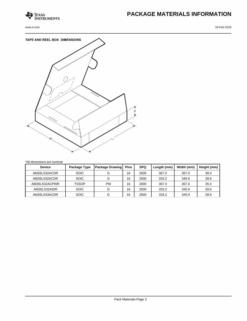
*All dimensions are nominal
Device Package Type Package Drawing Pins SPQ Length (mm) Width (mm) Height (mm)
AM26LS32ACDR SOIC D 16 2500 367.0 367.0 38.0
AM26LS32ACDR SOIC D 16 2500 333.2 345.9 28.6
AM26LS32ACPWR TSSOP PW 16 2000 367.0 367.0 35.0
AM26LS32AIDR SOIC D 16 2500 333.2 345.9 28.6
AM26LS33ACDR SOIC D 16 2500 333.2 345.9 28.6
PACKAGE MATERIALS INFORMATION
www.ti.com 24-Feb-2016
Pack Materials-Page 2


IMPORTANT NOTICE
Texas Instruments Incorporated and its subsidiaries (TI) reserve the right to make corrections, enhancements, improvements and otherchanges to its semiconductor products and services per JESD46, latest issue, and to discontinue any product or service per JESD48, latestissue. Buyers should obtain the latest relevant information before placing orders and should verify that such information is current andcomplete. All semiconductor products (also referred to herein as “components”) are sold subject to TI’s terms and conditions of salesupplied at the time of order acknowledgment.TI warrants performance of its components to the specifications applicable at the time of sale, in accordance with the warranty in TI’s termsand conditions of sale of semiconductor products. Testing and other quality control techniques are used to the extent TI deems necessaryto support this warranty. Except where mandated by applicable law, testing of all parameters of each component is not necessarilyperformed.TI assumes no liability for applications assistance or the design of Buyers’ products. Buyers are responsible for their products andapplications using TI components. To minimize the risks associated with Buyers’ products and applications, Buyers should provideadequate design and operating safeguards.TI does not warrant or represent that any license, either express or implied, is granted under any patent right, copyright, mask work right, orother intellectual property right relating to any combination, machine, or process in which TI components or services are used. Informationpublished by TI regarding third-party products or services does not constitute a license to use such products or services or a warranty orendorsement thereof. Use of such information may require a license from a third party under the patents or other intellectual property of thethird party, or a license from TI under the patents or other intellectual property of TI.Reproduction of significant portions of TI information in TI data books or data sheets is permissible only if reproduction is without alterationand is accompanied by all associated warranties, conditions, limitations, and notices. TI is not responsible or liable for such altereddocumentation. Information of third parties may be subject to additional restrictions.Resale of TI components or services with statements different from or beyond the parameters stated by TI for that component or servicevoids all express and any implied warranties for the associated TI component or service and is an unfair and deceptive business practice.TI is not responsible or liable for any such statements.Buyer acknowledges and agrees that it is solely responsible for compliance with all legal, regulatory and safety-related requirementsconcerning its products, and any use of TI components in its applications, notwithstanding any applications-related information or supportthat may be provided by TI. Buyer represents and agrees that it has all the necessary expertise to create and implement safeguards whichanticipate dangerous consequences of failures, monitor failures and their consequences, lessen the likelihood of failures that might causeharm and take appropriate remedial actions. Buyer will fully indemnify TI and its representatives against any damages arising out of the useof any TI components in safety-critical applications.In some cases, TI components may be promoted specifically to facilitate safety-related applications. With such components, TI’s goal is tohelp enable customers to design and create their own end-product solutions that meet applicable functional safety standards andrequirements. Nonetheless, such components are subject to these terms.No TI components are authorized for use in FDA Class III (or similar life-critical medical equipment) unless authorized officers of the partieshave executed a special agreement specifically governing such use.Only those TI components which TI has specifically designated as military grade or “enhanced plastic” are designed and intended for use inmilitary/aerospace applications or environments. Buyer acknowledges and agrees that any military or aerospace use of TI componentswhich have not been so designated is solely at the Buyer's risk, and that Buyer is solely responsible for compliance with all legal andregulatory requirements in connection with such use.TI has specifically designated certain components as meeting ISO/TS16949 requirements, mainly for automotive use. In any case of use ofnon-designated products, TI will not be responsible for any failure to meet ISO/TS16949.
Products ApplicationsAudio www.ti.com/audio Automotive and Transportation www.ti.com/automotiveAmplifiers amplifier.ti.com Communications and Telecom www.ti.com/communicationsData Converters dataconverter.ti.com Computers and Peripherals www.ti.com/computersDLP® Products www.dlp.com Consumer Electronics www.ti.com/consumer-appsDSP dsp.ti.com Energy and Lighting www.ti.com/energyClocks and Timers www.ti.com/clocks Industrial www.ti.com/industrialInterface interface.ti.com Medical www.ti.com/medicalLogic logic.ti.com Security www.ti.com/securityPower Mgmt power.ti.com Space, Avionics and Defense www.ti.com/space-avionics-defenseMicrocontrollers microcontroller.ti.com Video and Imaging www.ti.com/videoRFID www.ti-rfid.comOMAP Applications Processors www.ti.com/omap TI E2E Community e2e.ti.comWireless Connectivity www.ti.com/wirelessconnectivity
Mailing Address: Texas Instruments, Post Office Box 655303, Dallas, Texas 75265Copyright © 2016, Texas Instruments Incorporated