slls996a – september 2009– revised april 2010 8-channel
TRANSCRIPT

VN
VP
HV TX LV RX
1 Channel
of TX810
TX810www.ti.com SLLS996A –SEPTEMBER 2009–REVISED APRIL 2010
8-Channel, Programmable T/R Switch for UltrasoundCheck for Samples: TX810
1FEATURES DESCRIPTION2• Compact T/R Switch for Ultrasound The TX810 provides an integrated solution for a wide
range of ultrasound applications. It is an 8 channel,• Flexible Programmabilitycurrent programmable, transmit/receive switch in a– 8 Bias Current Settingssmall 6mm × 6mm package.
– 8 Power/Performance CombinationsThe internal diodes limit the output voltage when high– Easy Power-Up/Down controlvoltage transmitter signals are applied to the input.
• Fast Wake Up Time While the insertion loss of TX810 is minimized duringreceive mode.• Dual Supply Operation
• Optimized Insertion Loss Unlike conventional T/R switches, the TX810 containsa 3-bit interface used to program bias current from7mA to 0mA for different performance and powerAPPLICATIONSrequirements. When the TX810 bias current is set as• Medical Ultrasound0mA (i.e., high-impedance mode), the device is• Industrial Ultrasoundconfigured as power-down mode. In thehigh-impedance mode, TX810 does not addadditional load to high-voltage transmitters. Inaddition, the device can wake up from power-downmode in less than 1µs. With these advancedprogrammability features, significant power savingcan be achieved in systems.
Figure 1. Block Diagram of TX810
1
Please be aware that an important notice concerning availability, standard warranty, and use in critical applications of TexasInstruments semiconductor products and disclaimers thereto appears at the end of this data sheet.
2PowerPAD is a trademark of Texas Instruments.
PRODUCTION DATA information is current as of publication date. Copyright © 2009–2010, Texas Instruments IncorporatedProducts conform to specifications per the terms of the TexasInstruments standard warranty. Production processing does notnecessarily include testing of all parameters.

TX810SLLS996A –SEPTEMBER 2009–REVISED APRIL 2010 www.ti.com
These devices have limited built-in ESD protection. The leads should be shorted together or the device placed in conductive foamduring storage or handling to prevent electrostatic damage to the MOS gates.
ORDERING INFORMATION (1)
TRANSPORT MEDIA, OPERATING TEMPERATUREPACKAGED DEVICES PACKAGE TYPE QUANTITY RANGE
TX810IRHHT Tape and Reel, 250S-PVQFN-N36 0~70°C
TX810IRHHR Tape and Reel, 2500
(1) For the most current package and ordering information, see the Package Option Addendum at the end of this document, or see the TIwebsite at www.ti.com.
ABSOLUTE MAXIMUM RATINGS (1)
over operating free-air temperature range (unless otherwise noted)
VALUE UNIT
Supply Voltage, VD -0.3 ~ +6 V
Supply Voltage, VP -0.3 ~ +6 V
Supply Voltage, VN -6 ~ +0.3 V
Supply Voltage, VB -0.3 ~ +6 V
Input AC voltage, INn ±100 V
Input at Vsub -6 ~ +0.3 V
Output current, IO 15 mA
Maximum junction temperature, continuous operation, long term reliability (2) TJ 125°C
Storage temperature range, Tstg -55°C to 150°C
HBM 500 V
ESD ratings CDM 750 V
MM 200 V
(1) Stresses above those listed under absolute maximum ratings may cause permanent damage to the device. These are stress ratingsonly and functional operation of the device at these or any other conditions beyond those indicated under “recommended operatingconditions” is not implied Exposure to absolute maximum rated conditions for extended periods may degrade device reliability.
(2) The absolute maximum junction temperature for continuous operation is limited by the package constraints. Operation above thistemperature may result in reduced reliability and/or lifetime of the device.
THERMAL INFORMATIONTX810
THERMAL METRIC (1)RHH UNITS(OLFM Airflow Assumed)
36 PINS
qJA Junction-to-ambient thermal resistance (2) 29.7
qJC(top) Junction-to-case(top) thermal resistance (3) 27
qJB Junction-to-board thermal resistance (4) 7.2 °C/W
yJT Junction-to-top characterization parameter (5) 0.1
yJB Junction-to-board characterization parameter (6) 7.2
(1) For more information about traditional and new thermal metrics, see the IC Package Thermal Metrics application report, SPRA953.(2) The junction-to-ambient thermal resistance under natural convection is obtained in a simulation on a JEDEC-standard, High-K board, as
specified in JESD51-7, in an environment described in JESD51-2a.(3) The junction-to-case(top) thermal resistance is obtained by simulating a cold plate test on the package top. No specific JEDEC-standard
test exists, but a close description can be found in the ANSI SEMI standard G30-88.(4) The junction-to-board thermal resistance is obtained by simulating in an environment with a ring cold plate fixture to control the PCB
temperature, as described in JESD51-8.(5) The junction-to-top characterization parameter, yJT, estimates the junction temperature of a device in a real system and is extracted
from the simulation data for obtaining qJA, using a procedure described in JESD51-2a (sections 6 and 7).(6) The junction-to-board characterization parameter, yJB estimates the junction temperature of a device in a real system and is extracted
from the simulation data for obtaining qJA , using a procedure described in JESD51-2a (sections 6 and 7).
2 Submit Documentation Feedback Copyright © 2009–2010, Texas Instruments Incorporated
Product Folder Link(s) :TX810

VP
VD
B3
IN8
IN2
OU
T2
B1
VB
IN1
7
6
5
4
3
2
1
14131110 12
OU
T1
OUT4
OUT3
OUT5
36 34
22
24
25
3031323335
15 16
19
20
21
23
IN7
B2
VN
NC
NC
8
9
17 18
26
27
29 28
GN
DG
ND
GN
DG
ND
GND
OUT6
GND
OU
T8
OU
T7
GN
DG
ND
IN3
IN4
IN6
IN5
GND
NC
GND
TX810
PowerPAD™
TX810www.ti.com SLLS996A –SEPTEMBER 2009–REVISED APRIL 2010
DEVICE INFORMATION
PIN FUNCTIONSPIN
DESCRIPTIONNUMBER NAME
1, 3, 7, 9, 10, 12, 34, INn Inputs for Channel n36
16, 18, 19, 21, 25, 27, OUTn Outputs for Channel n28, 30
33 VD Logic Supply Voltage; +2.5 V to +5 V; bypass to ground with 0.1 µF and 10 µF capacitors
31 VP Positive Supply Voltage; +5 V; bypass to ground with 0.1 µF and 10 µF capacitors
15 VN Negative Supply Voltage; –5 V; bypass to ground with 0.1 µF and 10 µF capacitors
13 VB Bias voltage; connect to 0 V (GND) for ±5 V operation
2, 8, 11, 14, 17, 20, 26, GND Ground29, 32, 35
24 B1 Bit 1; Current program bit
23 B2 Bit 2; Current program bit
22 B3 Bit 3; Current program bit
4, 5, 6 NC No internal connection.
PowerPAD™ of the package. –5 V to 0 V for ±5 V operation. The thermal pad is needed for thermal0 Vsub dissipation.
PQFN (RHH) Package6 × 6mm, 0.5mm Pitch
(Top View)
Copyright © 2009–2010, Texas Instruments Incorporated Submit Documentation Feedback 3
Product Folder Link(s) :TX810

TX810SLLS996A –SEPTEMBER 2009–REVISED APRIL 2010 www.ti.com
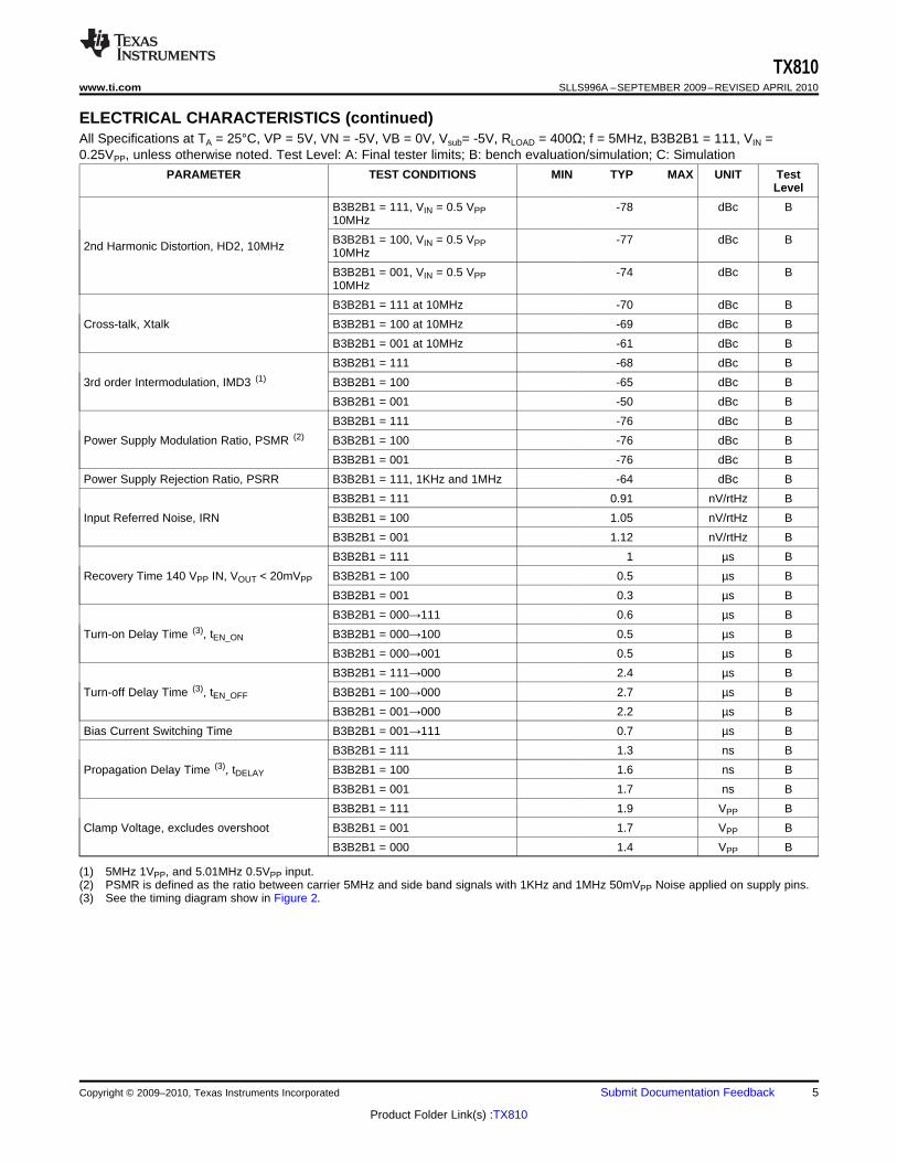
ELECTRICAL CHARACTERISTICSAll Specifications at TA = 25°C, VP = 5V, VN = -5V, VB = 0V, Vsub= -5V, RLOAD = 400Ω; f = 5MHz, B3B2B1 = 111, VIN =0.25VPP, unless otherwise noted. Test Level: A: Final tester limits; B: bench evaluation/simulation; C: Simulation
PARAMETER TEST CONDITIONS MIN TYP MAX UNIT TestLevel
DC POWER SPECIFICATIONS
Positive Supply VP 5V B
Negative Supply VN -5
Quiescent current, VP, VN No Signal 50 µA A
Substrate Voltage, VSUB PowerPAD™ VN 0 V B
Digital Supply, VD 2.5 5 V B
Quiescent current, VD No Signal 50 µA A
Bias current, VP, VN path B3B2B1 = 001 1.25 1 0.75 mA/CH A
Bias current, VP, VN path B3B2B1 = 111 5.95 7 8.05 mA/CH A
Any output; B3B2B1 = 000; NoLeakage Current 0.5 µA AInput
LOGIC INPUTS
Logic High Input Voltage; VIH 2 VD V A
Logic High Input Current; IIH 20 µA A
Logic Low Input Voltage; VIL 0 0.4 V A
Logic Low Input Current; IIL Input 20 µA A
Capacitance, CIN 5 pF C
POWER DISSIPATION All channels
Power-Down Dissipation B3B2B1 = 000; no signal 200 µW A
B3B2B1 = 001; no signal 80 92 mW ATotal Power Dissipation
B3B2B1 = 111; no signal 560 644 mW A
AC SPECIFICATIONS
1 µs positive and negative pulseapplied seperately at -90 90 V A
Input Amplitude, VIN PRF = 10 kHz
CW mode (continuous wave) -10 10 V B
B3B2B1 = 111 -0.9 -1.8 dB A
B3B2B1 = 100 -1.1 -1.8 dB A
Insertion loss, IL B3B2B1 = 001 -1.3 -2 dB A
B3B2B1 = 111, RLOAD = 50Ω -4.1 dB B
B3B2B1 = 001, RLOAD = 50Ω -7 dB B
Channel to channel IL matching B3B2B1 = 111 0.06 dB B
Insertion Loss, IL B3B2B1 = 111, at 20MHz -0.9 dB B
B3B2B1 = 111, RLOAD = 50 Ω 30 Ω B
B3B2B1 = 001, RLOAD = 50 Ω 62 Ω BEquivalent Resistance, RON
B3B2B1 = 111 44 Ω B
B3B2B1 = 001 67 Ω B
B3B2B1 = 111 140 MHz B
-3dB Bandwidth, BW B3B2B1 = 100 115 MHz B
B3B2B1 = 001 65 MHz B
B3B2B1 = 111, VIN = 0.5VPP -74 dBc B5MHz
B3B2B1 = 100, VIN = 0.5VPP -74 dBc B2nd Harmonic Distortion, HD2, 5MHz 5MHz
B3B2B1 = 001, VIN = 0.5VPP -73 dBc B5MHz
4 Submit Documentation Feedback Copyright © 2009–2010, Texas Instruments Incorporated
Product Folder Link(s) :TX810
TX810www.ti.com SLLS996A –SEPTEMBER 2009–REVISED APRIL 2010
ELECTRICAL CHARACTERISTICS (continued)All Specifications at TA = 25°C, VP = 5V, VN = -5V, VB = 0V, Vsub= -5V, RLOAD = 400Ω; f = 5MHz, B3B2B1 = 111, VIN =0.25VPP, unless otherwise noted. Test Level: A: Final tester limits; B: bench evaluation/simulation; C: Simulation
PARAMETER TEST CONDITIONS MIN TYP MAX UNIT TestLevel
B3B2B1 = 111, VIN = 0.5 VPP -78 dBc B10MHz
B3B2B1 = 100, VIN = 0.5 VPP -77 dBc B2nd Harmonic Distortion, HD2, 10MHz 10MHz
B3B2B1 = 001, VIN = 0.5 VPP -74 dBc B10MHz
B3B2B1 = 111 at 10MHz -70 dBc B
Cross-talk, Xtalk B3B2B1 = 100 at 10MHz -69 dBc B
B3B2B1 = 001 at 10MHz -61 dBc B
B3B2B1 = 111 -68 dBc B
3rd order Intermodulation, IMD3 (1) B3B2B1 = 100 -65 dBc B
B3B2B1 = 001 -50 dBc B
B3B2B1 = 111 -76 dBc B
Power Supply Modulation Ratio, PSMR (2) B3B2B1 = 100 -76 dBc B
B3B2B1 = 001 -76 dBc B
Power Supply Rejection Ratio, PSRR B3B2B1 = 111, 1KHz and 1MHz -64 dBc B
B3B2B1 = 111 0.91 nV/rtHz B
Input Referred Noise, IRN B3B2B1 = 100 1.05 nV/rtHz B
B3B2B1 = 001 1.12 nV/rtHz B
B3B2B1 = 111 1 µs B
Recovery Time 140 VPP IN, VOUT < 20mVPP B3B2B1 = 100 0.5 µs B
B3B2B1 = 001 0.3 µs B
B3B2B1 = 000→111 0.6 µs B
Turn-on Delay Time (3), tEN_ON B3B2B1 = 000→100 0.5 µs B
B3B2B1 = 000→001 0.5 µs B
B3B2B1 = 111→000 2.4 µs B
Turn-off Delay Time (3), tEN_OFF B3B2B1 = 100→000 2.7 µs B
B3B2B1 = 001→000 2.2 µs B
Bias Current Switching Time B3B2B1 = 001→111 0.7 µs B
B3B2B1 = 111 1.3 ns B
Propagation Delay Time (3), tDELAY B3B2B1 = 100 1.6 ns B
B3B2B1 = 001 1.7 ns B
B3B2B1 = 111 1.9 VPP B
Clamp Voltage, excludes overshoot B3B2B1 = 001 1.7 VPP B
B3B2B1 = 000 1.4 VPP B
(1) 5MHz 1VPP, and 5.01MHz 0.5VPP input.(2) PSMR is defined as the ratio between carrier 5MHz and side band signals with 1KHz and 1MHz 50mVPP Noise applied on supply pins.(3) See the timing diagram show in Figure 2.
Copyright © 2009–2010, Texas Instruments Incorporated Submit Documentation Feedback 5
Product Folder Link(s) :TX810

tEN_ON tEN_OFF
tDELAY
INPUT
B3/B2/B1
OUTPUT
VN
VP
1 Channel
of TX810
Signal
Source
Test
Equipment
RIN RLOAD
t − Time − sm
1.5
0.5
Ou
tpu
tA
mp
litu
de
−V
-0.5
1 2.5 30.5-0.5 1.5 2
-2
-1
0
1
-1.5
2
0
80
20
Inp
ut
Am
plitu
de
−V
-20
-100
-60
0
40
-80
Bias = 7 mA
-40
60
100
Output
Input
Insertion Loss − dB
400
350
Un
itA
mo
un
t
100
-0.9
4
0
50
200
300
150
250
-0.9
2
-0.9
5
-0.9
-0.9
3
-0.8
5
-0.9
1
-0.8
9
-0.8
8
-0.8
7
-0.8
6
1890 Units,
Bias = 7 mA,
R = N/AIN
TX810SLLS996A –SEPTEMBER 2009–REVISED APRIL 2010 www.ti.com
Figure 2. Timing Diagram
TYPICAL CHARACTERISTICSAll Specifications at TA = 25°C, VP = 5V, VN = -5V, VB = 0V, VSUB = -5V, RIN = 75Ω, RLOAD = 400Ω;
f = 5MHz, B3B2B1=111, VIN = 0.25VPP, unless otherwise noted.
A typical bench setup is shown in Figure 3.
Figure 3. Typical Test Setup
AC coupling is used between High voltage pulser and TX810. Theinput signal is a combination of 0.25Vpp signal followed by a 1-cycle140Vpp pulse
Figure 4. Insertion Loss Distribution Figure 5. Recovery Time With Small Input Signal
6 Submit Documentation Feedback Copyright © 2009–2010, Texas Instruments Incorporated
Product Folder Link(s) :TX810

Bias Current − mA
-60
-62
Cro
ssta
lk−
dB
c
-74
2 71 63 4 5
-70
-64
10MHz
5MHz
-72
-68
-66
t − Time − sm
Ou
tpu
tA
mp
litu
de
−V
10 25 305-5 15 20
-0.04
0.04
0
80
20
Inp
ut
Am
plitu
de
−V
-20
-100
-60
0
40
-80
-40
60
100
Output
Input
-0.03
0
-0.05
-0.02
-0.01
0.03
0.02
0.01
0.05
Bias = 7 mA,
R = 50LOAD W
Bias Current − mA
-60
-62
2n
d H
arm
on
ic D
isto
rti
on
−d
Bc
-74
2 6 71 3 4 5
-80
-78
-70
-64
10MHz
5MHz
V = 500 mVIN PP
-76
-72
-68
-66
Bias Current − mA
1.4
1.2
Inp
ut
Refe
rred
No
ise
−n
V/
Hz
√
0.4
2 6 71 3 4 5
0
0.2
10MHz
5MHz
1MHz
0.6
0.8
1
t − Time − sm
0.3
0.1Tri
gg
er
Am
plitu
de
−V
-0.1
1 7 830 62 4 5
-0.3
-0.2
4
0
3
1
5
0
-1
2
Trigger
TX810 Output
0.2
Am
plitu
de
−V
6
t − Time − sm
0.3
0.1
Tri
gg
er
Am
plitu
de
−V
-0.1
0.5 3.5 41.50 31 2 2.5
-0.3
-0.2
4
0
3
1
5
0
-1
2
Trigger
TX810 Output
0.2
Ou
tpu
tA
mp
litu
de
−V
-2
6
TX810www.ti.com SLLS996A –SEPTEMBER 2009–REVISED APRIL 2010
TYPICAL CHARACTERISTICS (continued)
All Specifications at TA = 25°C, VP = 5V, VN = -5V, VB = 0V, VSUB = -5V, RIN = 75Ω, RLOAD = 400Ω;f = 5MHz, B3B2B1=111, VIN = 0.25VPP, unless otherwise noted.
AC coupling is used between High voltage pulser and TX810. Theinput signal is a 1-cycle 140Vpp pulse
Figure 6. Recovery Time Without Signal Figure 7. Cross-talk vs. Bias Currents vs. Frequency
Figure 8. HD2 vs. Bias Current vs. Frequency Figure 9. Input Referred Noise vs. Bias Current vs. Frequency
Figure 10. Power On Response Time (0mA to 7mA) Figure 11. Power Down Response Time (7mA to 0mA)
Copyright © 2009–2010, Texas Instruments Incorporated Submit Documentation Feedback 7
Product Folder Link(s) :TX810

t − Time − sm
0.2
0.1
-0.15
-0.5
Am
plitu
de
−V
-0.1
0.5 3.5 41.50 31 2 2.5
-0.3
-0.25
-0.2
4
0.15
0.05
0
3
1
5
0
-1
2
TX810 Output
Trigger
TX810SLLS996A –SEPTEMBER 2009–REVISED APRIL 2010 www.ti.com
TYPICAL CHARACTERISTICS (continued)
All Specifications at TA = 25°C, VP = 5V, VN = -5V, VB = 0V, VSUB = -5V, RIN = 75Ω, RLOAD = 400Ω;f = 5MHz, B3B2B1=111, VIN = 0.25VPP, unless otherwise noted.
Figure 12. Bias Current Adjustment Response Time (1mA to 7mA)
8 Submit Documentation Feedback Copyright © 2009–2010, Texas Instruments Incorporated
Product Folder Link(s) :TX810
TX810www.ti.com SLLS996A –SEPTEMBER 2009–REVISED APRIL 2010
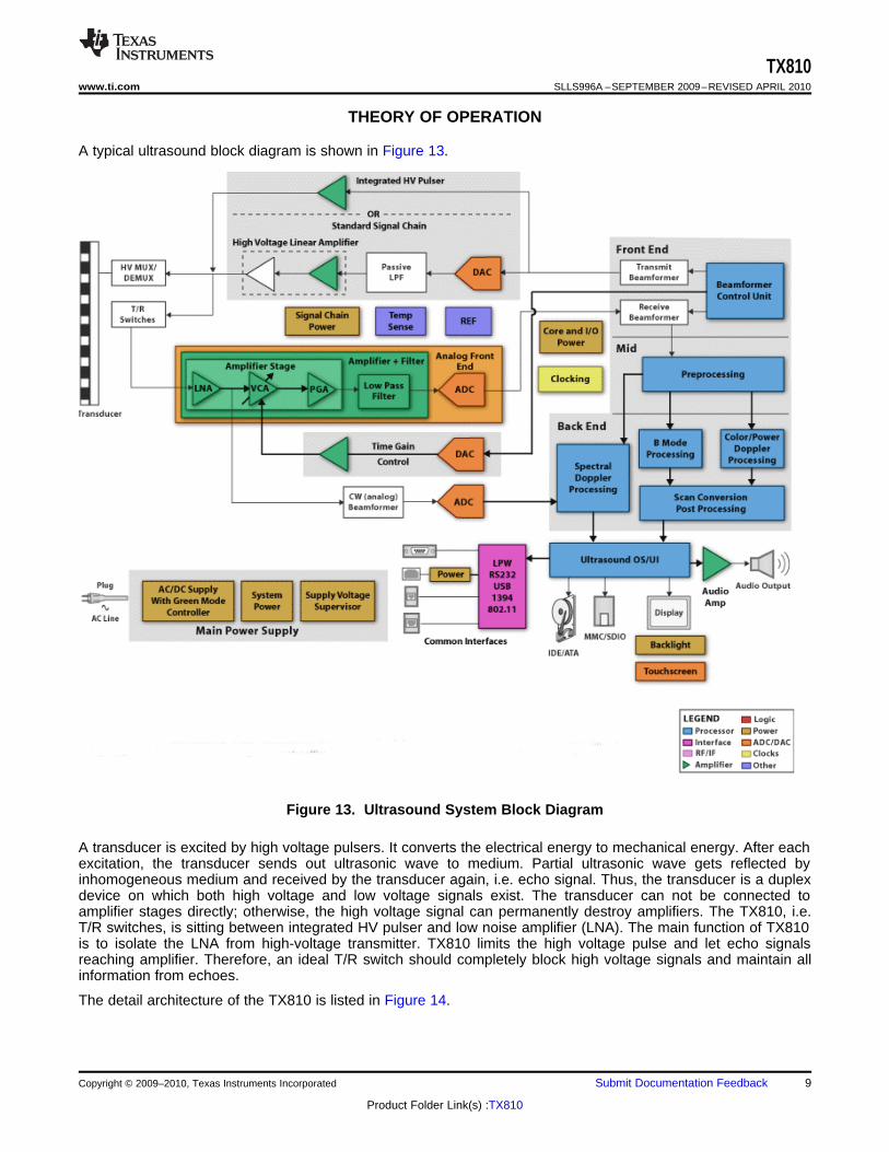
THEORY OF OPERATION
A typical ultrasound block diagram is shown in Figure 13.
Figure 13. Ultrasound System Block Diagram
A transducer is excited by high voltage pulsers. It converts the electrical energy to mechanical energy. After eachexcitation, the transducer sends out ultrasonic wave to medium. Partial ultrasonic wave gets reflected byinhomogeneous medium and received by the transducer again, i.e. echo signal. Thus, the transducer is a duplexdevice on which both high voltage and low voltage signals exist. The transducer can not be connected toamplifier stages directly; otherwise, the high voltage signal can permanently destroy amplifiers. The TX810, i.e.T/R switches, is sitting between integrated HV pulser and low noise amplifier (LNA). The main function of TX810is to isolate the LNA from high-voltage transmitter. TX810 limits the high voltage pulse and let echo signalsreaching amplifier. Therefore, an ideal T/R switch should completely block high voltage signals and maintain allinformation from echoes.
The detail architecture of the TX810 is listed in Figure 14.
Copyright © 2009–2010, Texas Instruments Incorporated Submit Documentation Feedback 9
Product Folder Link(s) :TX810

VN
HV TX LV RX
1 Channel
of TX810
VP
D0 D1 D2 D3 D4 D5 D6
D0 D1 D2 D3 D4 D5 D6
VB
D0~D6 is determined by
B1~B3 pins
L RLOAD
TX810SLLS996A –SEPTEMBER 2009–REVISED APRIL 2010 www.ti.com
Figure 14. TX810 Block Diagram
TX810 includes four parts: Diode Bridge, bias network, clamp diodes, and logic controller. A decoder is used toconvert 3-bit logic (B1 to B3) input to 7 control signals (D0 to D6) for 7 MOSFET switches. +2.5V to +5V logicinput is level shifted internally to drive the switches. The bias current of the bridge diode is adjustedproportionally by these switches. When all switches are on, the bias current is 7mA. Each bit difference willadjust the bias current approximately 1mA. When all switches are off, the TX810 enters the power down mode.Comparing to discrete T/R switches, TX810 can be shut down and turned on quickly as shown in the typicalcharacteristics plots. Considering the low duty cycle of ultrasound imaging, significant power saving can beachieved.
All 6 diodes are high-voltage Schottky diodes to achieve fast recovery time. Following the bridge, a pair ofback-to-back diode limits the output voltage of TX810 to about 2Vpp. Different power/performance combinationcan be selected by users. The TX810 is specified to operate at ±5V and VB is biased at 0V. The characteristicsof the T/R switch are mainly determined by bias currents. Lower power can be achieved with lower supplyvoltages. Also, Table 1 shows the relationship among bias current, insertion loss, input noise, powerconsumption and equivalent resistance.
Table 1. Bias current vs Performance
Test Conditions: VP = 5V, VN = -5V; VB = 0V; RLOAD = 50ΩB3 B2 B1 I (mA) IL (dB) IRN (nV/rtHz) RON (Ω) Power (mW/CH)
0 0 0 0 N/A N/A High Impedance 0
0 0 1 1 -7 1.12 62 10
0 1 0 2 -5.6 1.10 45 20
0 1 1 3 -5 1.09 39 30
1 0 0 4 -4.6 1.05 35 40
1 0 1 5 -4.4 0.99 33 50
1 1 0 6 -4.2 0.95 31 60
1 1 1 7 -4.1 0.91 30 70
10 Submit Documentation Feedback Copyright © 2009–2010, Texas Instruments Incorporated
Product Folder Link(s) :TX810
TX810www.ti.com SLLS996A –SEPTEMBER 2009–REVISED APRIL 2010
APPLICATION INFORMATION
Similar to discrete T/R switch solutions, external components can be used to optimize system performance.Inductor L and resistor RLOAD before the low voltage receiver amplifier (LVRx) can improve overload recoverytime and reduce reflection. The L acts as a high pass filter thus overshoot or recovery response spikes can besuppressed to minimal. The L and RLOAD terminate the entire signal path and can reduce reflection; thereforeaxial resolution in ultrasound image might be improved. However, the combined impedance of L and RLOAD mayaffect the system sensitivity. The insertion loss of T/R switch is determined by the input impedance of receiveramplifier and RON of the TX810. L also creates a DC path for any offset caused by mismatching.The inductor canbe as low as 10s µH to suppress low frequency signals from transmitter, transducer, multiplexer, and TX810. Theoptimization of L and RLOAD is always an important topic for system designers. AC coupling are typically usedbetween transmitter and T/R switch or T/R switch and amplifier. Thus amplifiers with DC biased inputs will notinterference with T/R switch.
One challenge for integrating multiple channel circuits on a small package is how to reduce cross talk. Inultrasound systems, acoustic cross talk from adjacent transducer elements is a dominant source. The cross talkfrom transducer elements is in a range of -30 to -35dBc for array transducers. Circuit cross talk is usually at least20dB better than the transducer cross talk. The special considerations were implemented in both TX810 designand layout. The cross talk among TX810 channels is reduced to below -60 dBc as show in the specificationtable.
In ultrasound Doppler applications, modulation effect in system can influence image quality and sensitivity.Ultrasound system is a complex mixed-signal system with all kinds of digital and analog circuits. Digital signalsand clock signals can contaminate analog signals on system level or on chip level. Nonlinear components, suchas transistors and diodes, can modulate noise and contaminate signals. In Doppler applications, the Dopplersignal frequency could range from 20Hz to >50KHz. Meanwhile, multiple system clocks are also in this range,such as frame clock, image line clock, and etc. These noise signals could enter chip through ground and powersupply pins. It is important to study the power supply modulation ratio (PSMR) at chip level. Noise signal withcertain frequency and amplitude can be applied on supply pins. Side band signals could be found if modulationeffect exists. The PSMR is expressed as an amplitude ratio between carrier and side band signals. BesidePSMR, 3rd order intermodulation ratio (IMD3) is a standard specification for mixed-signal ICs. Users can useIMD3 to estimate the potential artifact Doppler mirror signals. Both specs can be found in the specification table.
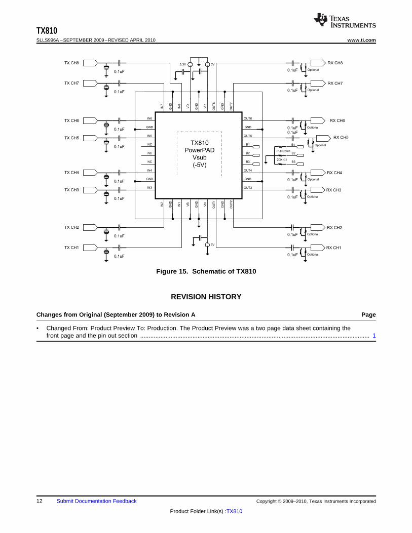
The schematic of the basic connection for TX810 is shown in Figure 15. Optional inductors and resistors can beused at TX810 outputs depending on transducer characteristics as discussed above. Standard decouplingcapacitors 0.1µF should be placed close to power supply pins. The pin out of TX810 is optimized for PCB layout.All signals are going from left to right straightly.
Copyright © 2009–2010, Texas Instruments Incorporated Submit Documentation Feedback 11
Product Folder Link(s) :TX810
IN6
IN5
GND
IN3
IN4
GND
GN
D
VD
B3
IN8
IN2
B1
VB
IN1
OUT4
OUT3
OUT5
B2
VN
GN
DG
ND
VP
GND
OUT6
GND
OU
T8
OU
T7
GN
D
NC
NC
NC
IN7
OU
T2
OU
T1
GN
D
GN
D
5V
3.3V
Optional
TX CH7
TX CH8
TX CH6
TX CH5
TX CH4
TX CH3
TX CH2
TX CH1
RX CH7
RX CH8
RX CH6
RX CH5
RX CH4
RX CH3
RX CH2
RX CH1
TX810
PowerPAD
Vsub
(-5V)
0.1uF
0.1uF
0.1uF
0.1uF
0.1uF
0.1uF
0.1uF
0.1uF
0.1uF
0.1uF
0.1uF0.1uF
0.1uF
0.1uF
0.1uF
0.1uF
B3
B1
B2
20K×3
Pull Down
5V
Optional
Optional
Optional
Optional
Optional
Optional
Optional
TX810SLLS996A –SEPTEMBER 2009–REVISED APRIL 2010 www.ti.com
Figure 15. Schematic of TX810
SPACERREVISION HISTORY
Changes from Original (September 2009) to Revision A Page
• Changed From: Product Preview To: Production. The Product Preview was a two page data sheet containing thefront page and the pin out section ........................................................................................................................................ 1
12 Submit Documentation Feedback Copyright © 2009–2010, Texas Instruments Incorporated
Product Folder Link(s) :TX810

PACKAGE OPTION ADDENDUM
www.ti.com 6-Aug-2021
Addendum-Page 1
PACKAGING INFORMATION
Orderable Device Status(1)
Package Type PackageDrawing
Pins PackageQty
Eco Plan(2)
Lead finish/Ball material
(6)
MSL Peak Temp(3)
Op Temp (°C) Device Marking(4/5)
Samples
TX810IRHHT ACTIVE VQFN RHH 36 250 RoHS & Green NIPDAU Level-2-260C-1 YEAR 0 to 70 TX810
(1) The marketing status values are defined as follows:ACTIVE: Product device recommended for new designs.LIFEBUY: TI has announced that the device will be discontinued, and a lifetime-buy period is in effect.NRND: Not recommended for new designs. Device is in production to support existing customers, but TI does not recommend using this part in a new design.PREVIEW: Device has been announced but is not in production. Samples may or may not be available.OBSOLETE: TI has discontinued the production of the device.
(2) RoHS: TI defines "RoHS" to mean semiconductor products that are compliant with the current EU RoHS requirements for all 10 RoHS substances, including the requirement that RoHS substancedo not exceed 0.1% by weight in homogeneous materials. Where designed to be soldered at high temperatures, "RoHS" products are suitable for use in specified lead-free processes. TI mayreference these types of products as "Pb-Free".RoHS Exempt: TI defines "RoHS Exempt" to mean products that contain lead but are compliant with EU RoHS pursuant to a specific EU RoHS exemption.Green: TI defines "Green" to mean the content of Chlorine (Cl) and Bromine (Br) based flame retardants meet JS709B low halogen requirements of <=1000ppm threshold. Antimony trioxide basedflame retardants must also meet the <=1000ppm threshold requirement.
(3) MSL, Peak Temp. - The Moisture Sensitivity Level rating according to the JEDEC industry standard classifications, and peak solder temperature.
(4) There may be additional marking, which relates to the logo, the lot trace code information, or the environmental category on the device.
(5) Multiple Device Markings will be inside parentheses. Only one Device Marking contained in parentheses and separated by a "~" will appear on a device. If a line is indented then it is a continuationof the previous line and the two combined represent the entire Device Marking for that device.
(6) Lead finish/Ball material - Orderable Devices may have multiple material finish options. Finish options are separated by a vertical ruled line. Lead finish/Ball material values may wrap to twolines if the finish value exceeds the maximum column width.
Important Information and Disclaimer:The information provided on this page represents TI's knowledge and belief as of the date that it is provided. TI bases its knowledge and belief on informationprovided by third parties, and makes no representation or warranty as to the accuracy of such information. Efforts are underway to better integrate information from third parties. TI has taken andcontinues to take reasonable steps to provide representative and accurate information but may not have conducted destructive testing or chemical analysis on incoming materials and chemicals.TI and TI suppliers consider certain information to be proprietary, and thus CAS numbers and other limited information may not be available for release.
In no event shall TI's liability arising out of such information exceed the total purchase price of the TI part(s) at issue in this document sold by TI to Customer on an annual basis.

TAPE AND REEL INFORMATION
*All dimensions are nominal
Device PackageType
PackageDrawing
Pins SPQ ReelDiameter
(mm)
ReelWidth
W1 (mm)
A0(mm)
B0(mm)
K0(mm)
P1(mm)
W(mm)
Pin1Quadrant
TX810IRHHT VQFN RHH 36 250 180.0 16.4 6.3 6.3 1.5 12.0 16.0 Q2
PACKAGE MATERIALS INFORMATION
www.ti.com 6-Aug-2021
Pack Materials-Page 1

*All dimensions are nominal
Device Package Type Package Drawing Pins SPQ Length (mm) Width (mm) Height (mm)
TX810IRHHT VQFN RHH 36 250 213.0 191.0 55.0
PACKAGE MATERIALS INFORMATION
www.ti.com 6-Aug-2021
Pack Materials-Page 2

www.ti.com
GENERIC PACKAGE VIEW
This image is a representation of the package family, actual package may vary.Refer to the product data sheet for package details.
VQFN - 1 mm max heightRHH 36PLASTIC QUAD FLATPACK - NO LEAD6 x 6, 0.5 mm pitch
4225440/A

www.ti.com
PACKAGE OUTLINE
6.15.9
6.15.9
1.00.8
0.050.00
2X 4
32X 0.5
2X 4
36X 0.650.45
36X 0.300.18
4.1 0.1
(0.2) TYP
VQFN - 1 mm max heightRHH0036BPLASTIC QUAD FLATPACK - NO LEAD
4225414/A 10/2019
0.08 C
0.1 C A B0.05
NOTES: 1. All linear dimensions are in millimeters. Any dimensions in parenthesis are for reference only. Dimensioning and tolerancing per ASME Y14.5M. 2. This drawing is subject to change without notice. 3. The package thermal pad must be soldered to the printed circuit board for thermal and mechanical performance.
PIN 1 INDEX AREA
SEATING PLANE
PIN 1 ID
SYMMEXPOSED
THERMAL PAD
SYMM
1
9
10 18
19
27
2836
37
SCALE 2.300
AB
C

www.ti.com
EXAMPLE BOARD LAYOUT
32X (0.5)
(R0.05) TYP
0.07 MAXALL AROUND
0.07 MINALL AROUND
36X (0.75)
36X (0.24)
(5.65)
(5.65)
( 4.1)
( 0.2) TYPVIA
(0.68)TYP
(1.8)TYP
(0.68)TYP
(1.8) TYP
VQFN - 1 mm max heightRHH0036BPLASTIC QUAD FLATPACK - NO LEAD
4225414/A 10/2019
NOTES: (continued) 4. This package is designed to be soldered to a thermal pad on the board. For more information, see Texas Instruments literature number SLUA271 (www.ti.com/lit/slua271).5. Vias are optional depending on application, refer to device data sheet. If any vias are implemented, refer to their locations shown on this view. It is recommended that vias under paste be filled, plugged or tented.
SYMM
SYMM
LAND PATTERN EXAMPLEEXPOSED METAL SHOWN
SCALE: 15X
SEE SOLDER MASKDETAIL
1
9
10 18
19
27
2836
37
METAL EDGE
SOLDER MASKOPENING
EXPOSEDMETAL
METAL UNDERSOLDER MASK
SOLDER MASKOPENING
EXPOSEDMETAL
NON SOLDER MASKDEFINED
(PREFERRED)SOLDER MASK DEFINED
SOLDER MASK DETAILS

www.ti.com
EXAMPLE STENCIL DESIGN
36X (0.75)
36X (0.24)
32X (0.5)
(5.65)
(5.65)
9X ( 1.16)
(R0.05) TYP
(1.36) TYP
(1.36)TYP
VQFN - 1 mm max heightRHH0036BPLASTIC QUAD FLATPACK - NO LEAD
4225414/A 10/2019
NOTES: (continued) 6. Laser cutting apertures with trapezoidal walls and rounded corners may offer better paste release. IPC-7525 may have alternate design recommendations.
SOLDER PASTE EXAMPLEBASED ON 0.125 MM THICK STENCIL
SCALE: 15X
EXPOSED PAD 3772% PRINTED SOLDER COVERAGE BY AREA UNDER PACKAGE
SYMM
SYMM
1
9
10 18
19
27
2836
37

IMPORTANT NOTICE AND DISCLAIMERTI PROVIDES TECHNICAL AND RELIABILITY DATA (INCLUDING DATASHEETS), DESIGN RESOURCES (INCLUDING REFERENCEDESIGNS), APPLICATION OR OTHER DESIGN ADVICE, WEB TOOLS, SAFETY INFORMATION, AND OTHER RESOURCES “AS IS”AND WITH ALL FAULTS, AND DISCLAIMS ALL WARRANTIES, EXPRESS AND IMPLIED, INCLUDING WITHOUT LIMITATION ANYIMPLIED WARRANTIES OF MERCHANTABILITY, FITNESS FOR A PARTICULAR PURPOSE OR NON-INFRINGEMENT OF THIRDPARTY INTELLECTUAL PROPERTY RIGHTS.These resources are intended for skilled developers designing with TI products. You are solely responsible for (1) selecting the appropriateTI products for your application, (2) designing, validating and testing your application, and (3) ensuring your application meets applicablestandards, and any other safety, security, or other requirements. These resources are subject to change without notice. TI grants youpermission to use these resources only for development of an application that uses the TI products described in the resource. Otherreproduction and display of these resources is prohibited. No license is granted to any other TI intellectual property right or to any third partyintellectual property right. TI disclaims responsibility for, and you will fully indemnify TI and its representatives against, any claims, damages,costs, losses, and liabilities arising out of your use of these resources.TI’s products are provided subject to TI’s Terms of Sale (https:www.ti.com/legal/termsofsale.html) or other applicable terms available eitheron ti.com or provided in conjunction with such TI products. TI’s provision of these resources does not expand or otherwise alter TI’sapplicable warranties or warranty disclaimers for TI products.IMPORTANT NOTICE
Mailing Address: Texas Instruments, Post Office Box 655303, Dallas, Texas 75265Copyright © 2021, Texas Instruments Incorporated