sllsec3f –september 2012–revised april 2016 ... · – industrial fieldbus – profibus –...
TRANSCRIPT
OUTx
GNDOGNDI
INx
VCCOVCCIIsolation Capacitor
ENx
Copyright © 2016, Texas Instruments Incorporated
Product
Folder
Sample &Buy
Technical
Documents
Tools &
Software
Support &Community
An IMPORTANT NOTICE at the end of this data sheet addresses availability, warranty, changes, use in safety-critical applications,intellectual property matters and other important disclaimers. PRODUCTION DATA.
ISO7631FM, ISO7631FC, ISO7641FCSLLSEC3F –SEPTEMBER 2012–REVISED APRIL 2016
ISO76x1 Low-Power Triple and Quad-Channels Digital Isolators
1
1 Features1• Signaling Rate: 150 Mbps (M-Grade), 25 Mbps
(C-Grade)• Robust Design with Integrated Noise Filter
(C-Grade)• Low Power Consumption, Typical ICC per Channel
(3.3-V Supplies):– ISO7631FM: 2 mA at 10 Mbps– ISO7631FC: 1.5 mA at 10 Mbps– ISO7641FC: 1.3 mA at 10 Mbps
• Extremely-Low ICC_disable (C-Grade)• Low Propagation Delay: 7 ns Typical (M-Grade)• Output Defaults to Low-State in Fail-Safe Mode• Wide Temperature Range: –40°C to 125°C• 50 KV/µs Transient Immunity, Typical• Long Life With SiO2 Isolation Barrier• Operates From 2.7-V (M-Grade), 3.3-V and 5-V
Supply and Logic Levels• 2.7-V (M-Grade), 3.3-V and 5-V Level Translation• Wide Body SOIC-16 Package• Safety and Regulatory Approvals
– 2500 VRMS Isolation for 1 Minute per UL 1577– 4242 VPK Basic Insulation per DIN V VDE V
0884-10 and DIN EN 61010-1– CSA Component Acceptance Notice 5A, IEC
60950-1 and IEC 61010-1 End EquipmentStandards
– CQC Certification per GB4943.1-2011– TUV 3000 VRMS Reinforced Insulation
according to EN/UL/CSA 60950-1 andEN/UL/CSA 61010-1
2 Applications• Optocoupler Replacement in:
– Industrial Fieldbus– Profibus– Modbus– DeviceNet™ Data Buses
– Servo Control Interface– Motor Control– Power Supplies– Battery Packs
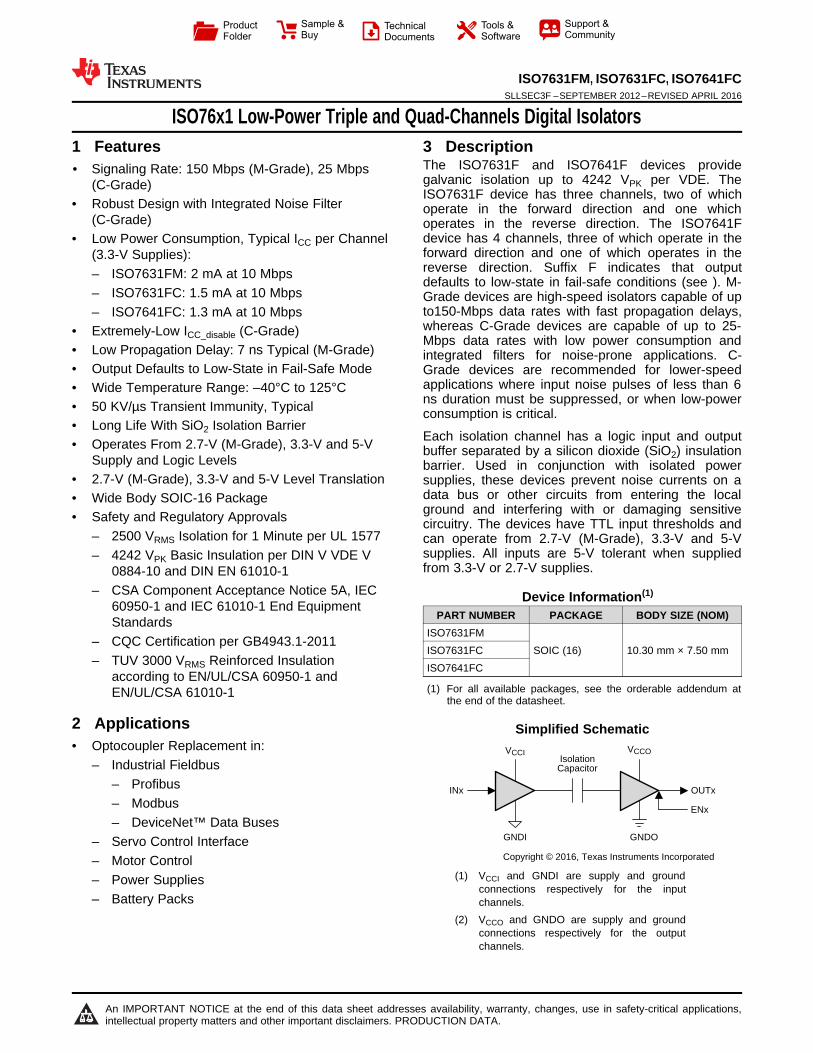
3 DescriptionThe ISO7631F and ISO7641F devices providegalvanic isolation up to 4242 VPK per VDE. TheISO7631F device has three channels, two of whichoperate in the forward direction and one whichoperates in the reverse direction. The ISO7641Fdevice has 4 channels, three of which operate in theforward direction and one of which operates in thereverse direction. Suffix F indicates that outputdefaults to low-state in fail-safe conditions (see ). M-Grade devices are high-speed isolators capable of upto150-Mbps data rates with fast propagation delays,whereas C-Grade devices are capable of up to 25-Mbps data rates with low power consumption andintegrated filters for noise-prone applications. C-Grade devices are recommended for lower-speedapplications where input noise pulses of less than 6ns duration must be suppressed, or when low-powerconsumption is critical.
Each isolation channel has a logic input and outputbuffer separated by a silicon dioxide (SiO2) insulationbarrier. Used in conjunction with isolated powersupplies, these devices prevent noise currents on adata bus or other circuits from entering the localground and interfering with or damaging sensitivecircuitry. The devices have TTL input thresholds andcan operate from 2.7-V (M-Grade), 3.3-V and 5-Vsupplies. All inputs are 5-V tolerant when suppliedfrom 3.3-V or 2.7-V supplies.
Device Information(1)
PART NUMBER PACKAGE BODY SIZE (NOM)ISO7631FM
SOIC (16) 10.30 mm × 7.50 mmISO7631FCISO7641FC
(1) For all available packages, see the orderable addendum atthe end of the datasheet.
Simplified Schematic
(1) VCCI and GNDI are supply and groundconnections respectively for the inputchannels.
(2) VCCO and GNDO are supply and groundconnections respectively for the outputchannels.
2
ISO7631FM, ISO7631FC, ISO7641FCSLLSEC3F –SEPTEMBER 2012–REVISED APRIL 2016 www.ti.com
Product Folder Links: ISO7631FM ISO7631FC ISO7641FC
Submit Documentation Feedback Copyright © 2012–2016, Texas Instruments Incorporated
Table of Contents1 Features .................................................................. 12 Applications ........................................................... 13 Description ............................................................. 14 Revision History..................................................... 25 Available Options................................................... 46 Pin Configuration and Functions ......................... 47 Specifications......................................................... 5
7.1 Absolute Maximum Ratings ...................................... 57.2 ESD Ratings.............................................................. 57.3 Recommended Operating Conditions....................... 57.4 Thermal Information ................................................. 67.5 Electrical Characteristics: VCC1 and VCC2 at 5 V ±
10%............................................................................ 67.6 Electrical Characteristics: VCC1 at 5 V ± 10% and
VCC2 at 3.3 V ± 10% .................................................. 67.7 Electrical Characteristics: VCC1 at 3.3 V ± 10% and
VCC2 at 5 V ± 10% ..................................................... 77.8 Electrical Characteristics: VCC1 and VCC2 at 3.3 V ±
10%............................................................................ 77.9 Electrical Characteristics: VCC1 and VCC2 at 2.7 V
(ISO7631FM Only)..................................................... 77.10 Power Dissipation Characteristics .......................... 77.11 Supply Current Characteristics: VCC1 and VCC2 at 5
V ± 10% ..................................................................... 87.12 Supply Current Characteristics: VCC1 at 5 V ± 10%
and VCC2 at 3.3 V ± 10% ........................................... 97.13 Supply Current Characteristics: VCC1 at 3.3 V ± 10%
and VCC2 at 5 V ± 10% .............................................. 97.14 Supply Current Characteristics: VCC1 and VCC2 at
3.3 V ± 10% ............................................................. 107.15 Supply Current Characteristics: VCC1 and VCC2 at
2.7 V (ISO7631FM Only) ........................................ 107.16 Switching Characteristics: VCC1 and VCC2 at 5 V ±
10%.......................................................................... 11
7.17 Switching Characteristics: VCC1 at 5 V ± 10% andVCC2 at 3.3 V ± 10% ................................................ 11
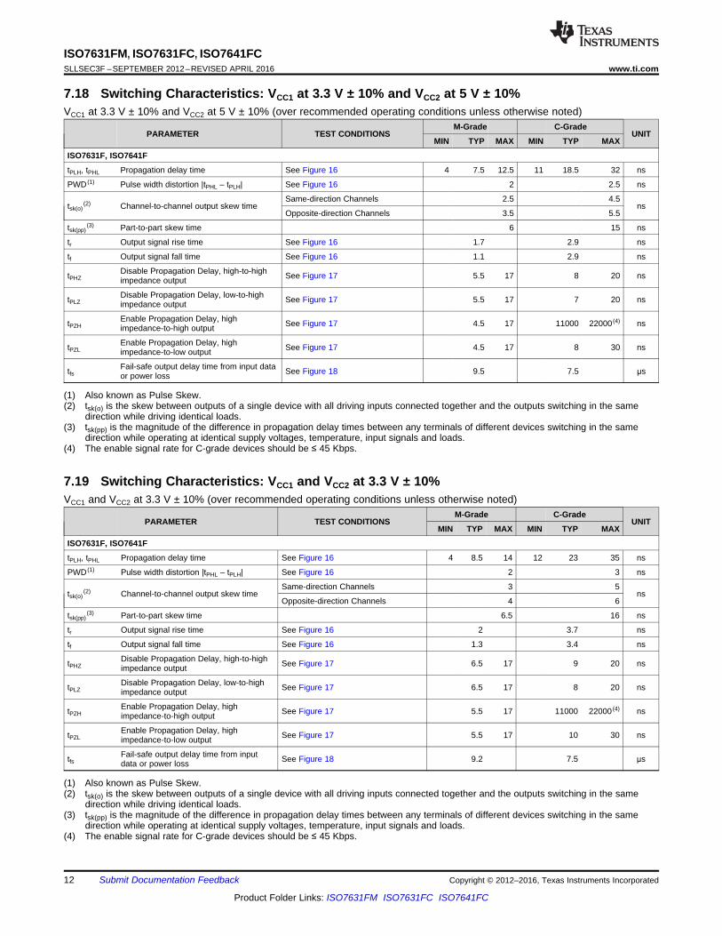
7.18 Switching Characteristics: VCC1 at 3.3 V ± 10% andVCC2 at 5 V ± 10% ................................................... 12
7.19 Switching Characteristics: VCC1 and VCC2 at 3.3 V ±10%.......................................................................... 12
7.20 Switching Characteristics: VCC1 and VCC2 at 2.7 V................................................................................. 13
7.21 Typical Characteristics .......................................... 148 Parameter Measurement Information ................ 179 Detailed Description ............................................ 19
9.1 Overview ................................................................. 199.2 Functional Block Diagram ....................................... 199.3 Feature Description................................................. 209.4 Device Functional Modes........................................ 23
10 Application and Implementation........................ 2410.1 Application Information.......................................... 2410.2 Typical Application ............................................... 24
11 Power Supply Recommendations ..................... 2712 Layout................................................................... 27
12.1 Layout Guidelines ................................................. 2712.2 Layout Example .................................................... 27
13 Device and Documentation Support ................. 2813.1 Documentation Support ........................................ 2813.2 Related Links ........................................................ 2813.3 Community Resources.......................................... 2813.4 Trademarks ........................................................... 2813.5 Electrostatic Discharge Caution............................ 2813.6 Glossary ................................................................ 28
14 Mechanical, Packaging, and OrderableInformation ........................................................... 28
4 Revision HistoryNOTE: Page numbers for previous revisions may differ from page numbers in the current version.
Changes from Revision E (August 2015) to Revision F Page
• Changed the ISO7631 pin image in the Pin Configuration and Functions section ............................................................... 4
Changes from Revision D (September 2013) to Revision E Page
• Added Pin Configuration and Functions section, ESD Ratings table, Feature Description section, Device FunctionalModes, Application and Implementation section, Power Supply Recommendations section, Layout section, Deviceand Documentation Support section, and Mechanical, Packaging, and Orderable Information section. ............................. 1
• Added 2.7-V (M-Grade), 3.3-V and 5-V Level Translation to Features section ..................................................................... 1• Deleted marked as column from Available Options table....................................................................................................... 4• Added Footnote 3 to Absolute Maximum Ratings table. ........................................................................................................ 5• Changed thermal metric values in the Thermal Information table. ........................................................................................ 6• Changed VCCX to VCCOin Electrical Characteristics: VCC1 and VCC2 at 5 V ± 10% table. ........................................................ 6• Added cross-reference to VI = VCCI in the Electrical Characteristics: VCC1 and VCC2 at 5 V ± 10% table. ....................... 6• Changed Footnote 1 of the Electrical Characteristics: VCC1 and VCC2 at 5 V ± 10% table for clarification. ..................... 6
3
ISO7631FM, ISO7631FC, ISO7641FCwww.ti.com SLLSEC3F –SEPTEMBER 2012–REVISED APRIL 2016
Product Folder Links: ISO7631FM ISO7631FC ISO7641FC
Submit Documentation FeedbackCopyright © 2012–2016, Texas Instruments Incorporated
• Added cross-reference to VI = VCCI in the Electrical Characteristics: VCC1 at 5 V ± 10% and VCC2 at 3.3 V ± 10%table. ....................................................................................................................................................................................... 6
• Added footnote to the Electrical Characteristics: VCC1 at 3.3 V ± 10% and VCC2 at 5 V ± 10% table. .............................. 7• Changed VCCX to VCCO in the Electrical Characteristics: VCC1 and VCC2 at 3.3 V ± 10% table. ........................................ 7• Changed footnote 1 in the Electrical Characteristics: VCC1 and VCC2 at 3.3 V ± 10% table for clarification. ..................... 7• Changed VCCX to VCCO in the Electrical Characteristics: VCC1 and VCC2 at 2.7 V table. ................................................... 7• Deleted IEC and for DW-16 Package from IEC Package Insulation and Safety-Related Specifications for DW-16
Package section. .................................................................................................................................................................. 20• Changed L(I01) MIN from 8.3 mm to 8 mm, L(IO2) MIN from 8.1 mm to 8 mm, and DIN IEC 60112 / VDE 0303 Part
1 to DIN EN 60112 (VDE 0303-11); IEC 60112 in the Package Insulation and Safety-Related Specifications table. ....... 20• Deleted footnote 2 from Package Insulation and Safety-Related Specifications IEC and for DW-16 Package from
IEC Package Insulation and Safety-Related Specifications for DW-16 Package section.. .................................................. 20• Changed VDE Standard to DIN V VDE V 0884-10 (VDE V 0084-10): 2006-12. ................................................................ 21• Changed the value for θJA from 72 °C/W to 77.5 °C/W for the Test Conditions and the values for Safety input,
output, or supply current max from 316, 482, and 643 to 293, 448 and 597 in the Safety Limiting Values table. ............. 22• Changed safety temperature to case temperature in Safety Limiting Values. ..................................................................... 22• Changed name of DW-16 θJC Thermal Derating Curve per IEC 64747-5-2 to Thermal Derating Curve for Safety
Limiting Current per VDE...................................................................................................................................................... 22• Changed Figure 22 in the Safety Limiting Values section. .................................................................................................. 22• Changed I/O schematics figure in Feature Description section. ......................................................................................... 23
Changes from Revision C (August 2013) to Revision D Page
• Deleted 2500 VRMS from Rated Isolation Data ....................................................................................................................... 4• Changed the Table 3, TUV column From: Certificate Number: U8V 13 07 77311 009 To: Certificate Number: U8V
13 09 77311 010................................................................................................................................................................... 21
Changes from Revision B (April 2013) to Revision C Page
• Changed the Description ........................................................................................................................................................ 1• Deleted ISO7640FC from the Available Options table ........................................................................................................... 4• Changed The ISO7631FC Rated Isolation values in the Available Options table ................................................................. 4• Deleted Graph ISO7640FC Supply Current Per Channel vs Data Rate .............................................................................. 14• Deleted Graph ISO7640FC Supply Current For All Channels vs Data Rate ....................................................................... 14• Added the TUV column to Table 3 ....................................................................................................................................... 21• Deleted ISO7640FC from the TYPICAL SUPPLY CURRENT EQUATIONS section .......................................................... 25• Deleted the ISO7640 circuit from the APPLICATION INFORMATION section.................................................................... 27
Changes from Revision A (September 2012) to Revision B Page
• Changed the VIOTM SPECIFICATION From: 4000 VPEAK to 4242 VPEAK............................................................................... 21• Changed Table 3: 4242 VPK To: 4000 VPK .......................................................................................................................... 21
Changes from Original (September 2012) to Revision A Page
• Changed Description text From: "applications where input noise pulses of less than 10 ns duration..."To:"applications where input noise pulses of less than 6 ns duration..."................................................................................ 1
• Added note Product Preview to ISO7640FC in the Available Options table.......................................................................... 4• Changed Input PU in the Function table From: Z To: 'Undetermined .................................................................................. 23

1
2
3
4
5
6
7
8 9
10
11
12
13
14
15
16
EN1
INA
GND1
INB
OUTC
NC
GND1
VCC1
GND2
GND2
OUTA
INC
OUTB
EN2
NC
VCC21
2
3
4
5
6
7
8 9
10
11
12
13
14
15
16
EN1
INA
GND1
INB
INC
OUTD
GND1
VCC1
GND2
GND2
OUTA
OUTC
OUTB
EN2
IND
VCC2
4
ISO7631FM, ISO7631FC, ISO7641FCSLLSEC3F –SEPTEMBER 2012–REVISED APRIL 2016 www.ti.com
Product Folder Links: ISO7631FM ISO7631FC ISO7641FC
Submit Documentation Feedback Copyright © 2012–2016, Texas Instruments Incorporated
(1) See the Table 3 table for detailed isolation ratings.
5 Available Options
PRODUCT RATED ISOLATION (1) PACKAGE INPUTTHRESHOLD DATA RATE INTEGRATED NOISE
FILTERCHANNEL
DIRECTION
ISO631FM 4242 VPK DW-16 ~1.5 V TTL 150 Mbps No 2 Forward,1 Reverse
ISO7631FC 4242 VPK DW-16 ~1.5 V TTL 25 Mbps Yes 2 Forward,1 Reverse
ISO7641FC 4242 VPK DW-16 ~1.5 V TTL 25 Mbps Yes 3 Forward,1 Reverse
6 Pin Configuration and Functions
ISO7641 DW Package16-Pin SOIC
Top View
ISO7631 DW Package16-Pin SOIC
Top View
Pin FunctionsPIN
I/O DESCRIPTIONNAME ISO7641 ISO7631
EN1 7 7 I Enables (when input is High or Open) or Disables (when input is Low) OUTD of ISO7641 andOUTC of ISO7631
EN2 10 10 I
Enables (when input is High or Open) or Disables (when input is Low) OUTA, OUTB, andOUTC of ISO7641Enables (when input is High or Open) or Disables (when input is Low) OUTA and OUTB ofISO7631
GND1 2, 8 2, 8 – Ground connection for VCC1
GND2 9, 15 9, 15 – Ground connection for VCC2
INA 3 3 I Input, channel AINB 4 4 I Input, channel BINC 5 12 I Input, channel CIND 11 – I Input, channel DNC – 6,11 – No Connect pins are floating with no internal connectionOUTA 14 14 O Output, channel AOUTB 13 13 O Output, channel BOUTC 12 5 O Output, channel COUTD 6 – O Output, channel DVCC1 1 1 – Power supply, VCC1
VCC2 16 16 – Power supply, VCC2

5
ISO7631FM, ISO7631FC, ISO7641FCwww.ti.com SLLSEC3F –SEPTEMBER 2012–REVISED APRIL 2016
Product Folder Links: ISO7631FM ISO7631FC ISO7641FC
Submit Documentation FeedbackCopyright © 2012–2016, Texas Instruments Incorporated
(1) Stresses beyond those listed under absolute maximum ratings may cause permanent damage to the device. These are stress ratingsonly and functional operation of the device at these or any other conditions beyond those indicated under Recommended OperatingConditions is not implied. Exposure to absolute-maximum-rated conditions for extended periods may affect device reliability.
(2) All voltage values except differential I/O bus voltages are with respect to the local ground terminal (GND1 or GND2) and are peakvoltage values.
(3) Maximum voltage must not exceed 6 V.
7 Specifications
7.1 Absolute Maximum RatingsSee (1)
MIN MAX UNITVCC1VCC2
(2) Supply voltage –0.5 6 V
Voltage INx, OUTx, ENx –0.5 6 (3) VIO Output current ±15 mATJ Maximum junction temperature 150 °CTSTG Storage temperature –65 150 °C
(1) JEDEC document JEP155 states that 500-V HBM allows safe manufacturing with a standard ESD control process.(2) JEDEC document JEP157 states that 250-V CDM allows safe manufacturing with a standard ESD control process.
7.2 ESD RatingsVALUE UNIT
V(ESD) Electrostatic discharge
Human body model (HBM), per ANSI/ESDA/JEDEC JS-001 (1) ±4000
VCharged-device model (CDM), per JEDEC specification JESD22-C101 (2)
±1500
Machine model (MM), JEDEC JESD22-A115-A ±200
7.3 Recommended Operating ConditionsMIN NOM MAX UNIT
VCC1, VCC2 Supply voltageM-Grade 2.7 5.5
VC-Grade 3 5.5
IOH High-level output current –4 mAIOL Low-level output current 4 mAVIH High-level input voltage 2 5.5 VVIL Low-level input voltage 0 0.8 V
tui Input pulse durationM-Grade: ≥3-V Operation 6.67
nsM-Grade: <3-V Operation 10C-Grade: ≥3-V Operation 40
1 / tui Signaling rateM-Grade: ≥3-V Operation 0 150
MbpsM-Grade: <3-V Operation 0 100C-Grade: ≥3-V Operation 0 25
TJ Junction temperature –40 136 °CTA Ambient temperature –40 25 125 °C

6
ISO7631FM, ISO7631FC, ISO7641FCSLLSEC3F –SEPTEMBER 2012–REVISED APRIL 2016 www.ti.com
Product Folder Links: ISO7631FM ISO7631FC ISO7641FC
Submit Documentation Feedback Copyright © 2012–2016, Texas Instruments Incorporated
(1) For more information about traditional and new thermal metrics, see the Semiconductor and IC Package Thermal Metrics applicationreport, SPRA953.
7.4 Thermal Information
THERMAL METRIC (1)ISO76x1Fx
UNITDW (SOIC)16 PINS
RθJA Junction-to-ambient thermal resistance 77.5 °C/WRθJC(top) Junction-to-case (top) thermal resistance 40.4 °C/WRθJB Junction-to-board thermal resistance 42.2 °C/WψJT Junction-to-top characterization parameter 15 °C/WψJB Junction-to-board characterization parameter 41.6 °C/W
(1) VCCI = Input-side supply voltage; VCCO = Output-side supply voltage
7.5 Electrical Characteristics: VCC1 and VCC2 at 5 V ± 10%VCC1 and VCC2 at 5 V ± 10% (over recommended operating conditions unless otherwise noted)
PARAMETER TEST CONDITIONSM-Grade C-Grade
UNITMIN TYP MAX MIN TYP MAX
VOH High-level output voltageIOH = –4 mA; see Figure 16 VCCO
(1) – 0.8 4.8 VCCO – 0.8 4.7V
IOH = –20 μA; see Figure 16 VCCO – 0.1 5 VCCO – 0.1 5
VOL Low-level output voltageIOL = 4 mA; see Figure 16 0.2 0.4 0.3 0.5
VIOL = 20 μA; see Figure 16 0 0.1 0 0.1
VI(HYS)Input threshold voltagehysteresis 450 450 mV
IIH High-level input current VIH = VCC at INx or ENx 10 10 μA
IIL Low-level input current VIL = 0 V at INx or ENx –10 -10 μA
CMTI Common-mode transientimmunity VI = VCCI
(1) or 0 V; see Figure 19 25 75 25 75 kV/μs
(1) VCCI = Input-side supply voltage
7.6 Electrical Characteristics: VCC1 at 5 V ± 10% and VCC2 at 3.3 V ± 10%VCC1 at 5 V ± 10% and VCC2 at 3.3 V ± 10% (over recommended operating conditions unless otherwise noted)
PARAMETER TEST CONDITIONSM-Grade C-Grade
UNITMIN TYP MAX MIN TYP MAX
VOHHigh-level outputvoltage
IOH = –4 mA; seeFigure 16
OUTx on VCC1 (5 V) side VCC1 – 0.8 4.8 VCC1 – 0.8 4.7
VOUTx on VCC2 (3.3 V) side VCC2 - 0.4 3 VCC2 - 0.6 2.9
IOH = –20 μA;see Figure 16
OUTx on VCC1 (5 V) side VCC1 – 0.1 5 VCC1 – 0.1 5
OUTx on VCC2 (3.3 V) side VCC2 – 0.1 3.3 VCC2 – 0.1 3.3
VOLLow-level outputvoltage
IOL = 4 mA; see Figure 16 0.2 0.4 0.3 0.5V
IOL = 20 μA; see Figure 16 0 0.1 0 0.1
VI(HYS)Input threshold voltagehysteresis 430 430 mV
IIH High-level input current VIH = VCC at INx or ENx 10 10 μA
IIL Low-level input current VIL = 0 V at INx or ENx -10 -10 μA
CMTI Common-modetransient immunity VI = VCCI
(1) or 0 V; see Figure 19 25 50 25 50 kV/μs

7
ISO7631FM, ISO7631FC, ISO7641FCwww.ti.com SLLSEC3F –SEPTEMBER 2012–REVISED APRIL 2016
Product Folder Links: ISO7631FM ISO7631FC ISO7641FC
Submit Documentation FeedbackCopyright © 2012–2016, Texas Instruments Incorporated
(1) VCCI = Input-side supply voltage
7.7 Electrical Characteristics: VCC1 at 3.3 V ± 10% and VCC2 at 5 V ± 10%VCC1 at 3.3 V ± 10% and VCC2 at 5 V ± 10% (over recommended operating conditions unless otherwise noted)
PARAMETER TEST CONDITIONSM-Grade C-Grade
UNITMIN TYP MAX MIN TYP MAX
VOH High-level output voltage
IOH = –4 mA; seeFigure 16
OUTx on VCC1 (3.3 V) side VCC1–0.4 3 VCC1-0.6 2.9
VOUTx on VCC2 (5 V) side VCC2–0.8 4.8 VCC2–0.8 4.7
IOH = –20 μA; seeFigure 16
OUTx on VCC1 (3.3 V) side VCC1–0.1 3.3 VCC1–0.1 3.3
OUTx on VCC2 (5 V) side VCC2–0.1 5 VCC2–0.1 5
VOL Low-level output voltageIOL = 4 mA; see Figure 16 0.2 0.4 0.3 0.5
VIOL = 20 μA; see Figure 16 0 0.1 0 0.1
VI(HYS)Input threshold voltagehysteresis 430 430 mV
IIH High-level input current VIH = VCC at INx or ENx 10 10 μA
IIL Low-level input current VIL = 0 V at INx or ENx -10 -10 μA
CMTI Common-mode transientimmunity VI = VCCI
(1) or 0 V; see Figure 19 25 50 25 50 kV/μs
(1) VCCI = Input-side supply voltage; VCCO = Output-side supply voltage
7.8 Electrical Characteristics: VCC1 and VCC2 at 3.3 V ± 10%VCC1 and VCC2 at 3.3 V ± 10% (over recommended operating conditions unless otherwise noted)
PARAMETER TEST CONDITIONSM-Grade C-Grade
UNITMIN TYP MAX MIN TYP MAX
VOHHigh-level outputvoltage
IOH = –4 mA; see Figure 16 VCCO(1) – 0.4 3 VCCO – 0.6 2.9
VIOH = –20 μA; see Figure 16 VCCO – 0.1 3.3 VCCO – 0.1 3.3
VOL Low-level output voltageIOL = 4 mA; see Figure 16 0.2 0.4 0.3 0.5
VIOL = 20 μA; see Figure 16 0 0.1 0 0.1
VI(HYS)Input threshold voltagehysteresis 425 425 mV
IIH High-level input current VIH = VCC at INx or ENx 10 10 μA
IIL Low-level input current VIL = 0 V at INx or ENx -10 -10 μA
CMTI Common-mode transientimmunity VI = VCCI
(1) or 0 V; see Figure 19 25 50 25 50 kV/μs
(1) Only M-Grade devices are recommended for operation down to 2.7 V supplies. For 2.7 V-operation, max data rate is 100 Mbps.(2) VCCI = Input-side supply voltage; VCCO = Output-side supply voltage
7.9 Electrical Characteristics: VCC1 and VCC2 at 2.7 V (ISO7631FM Only)VCC1 and VCC2 at 2.7 V (1) (over recommended operating conditions unless otherwise noted)
PARAMETER TEST CONDITIONS MIN TYP MAX UNIT
VOH High-level output voltageIOH = –4 mA; see Figure 16 VCCO
(2) – 0.5 2.4V
IOH = –20 μA; see Figure 16 VCCO – 0.1 2.7
VOL Low-level output voltageIOL = 4 mA; see Figure 16 0.2 0.4
VIOL = 20 μA; see Figure 16 0 0.1
VI(HYS) Input threshold voltage hysteresis 350 mV
IIH High-level input current VIH = VCC at INx or ENx 10 μA
IIL Low-level input current VIL = 0 V at INx or ENx -10 μA
CMTI Common-mode transient immunity VI = VCCI(2) or 0 V; see Figure 19 25 50 kV/μs
7.10 Power Dissipation CharacteristicsPARAMETER TEST CONDITIONS MIN TYP MAX UNIT
PD Maximum Device Power Dissipation
VCC1 = VCC2 = 5.5 V, TJ = 150°C,CL = 15 pFInput a 75 MHz 50% duty cyclesquare wave
399 mW

8
ISO7631FM, ISO7631FC, ISO7641FCSLLSEC3F –SEPTEMBER 2012–REVISED APRIL 2016 www.ti.com
Product Folder Links: ISO7631FM ISO7631FC ISO7641FC
Submit Documentation Feedback Copyright © 2012–2016, Texas Instruments Incorporated
7.11 Supply Current Characteristics: VCC1 and VCC2 at 5 V ± 10%VCC1 and VCC2 at 5 V ± 10% (over recommended operating conditions unless otherwise noted)
PARAMETER TEST CONDITIONSM-Grade C-Grade
UNITMIN TYP MAX MIN TYP MAX
ISO7631FICC1 Disable EN1 = EN2 = 0 V
2.5 4 1.1 1.9 mAICC2 3.7 5.4 1.5 2.6 mAICC1 DC to 1 Mbps
DC Signal: VI = VCC or 0 VAC Signal: All channels switching with squarewave clock input; CL = 15 pF
2.6 4.1 1.8 2.7 mAICC2 3.8 5.5 2.6 3.9 mAICC1 10 Mbps
3.3 4.5 2.7 3.7 mAICC2 4.9 6.6 3.9 5.3 mAICC1 25 Mbps
4.5 6 4.1 5.4 mAICC2 6.8 9 5.9 7.8 mAICC1 150 Mbps
15 19.5 Not Applicable mAICC2 22 30 Not Applicable mAISO7641FICC1 Disable EN1 = EN2 = 0 V
1.2 2.1 mAICC2 1.6 2.6 mAICC1 DC to 1 Mbps
DC Signal: VI = VCC or 0 V,AC Signal: All channels switching with squarewave clock input; CL = 15 pF
1.8 2.8 mAICC2 3.1 4.2 mAICC1 10 Mbps
3 4 mAICC2 4.9 6.1 mAICC1 25 Mbps
4.8 6 mAICC2 7.7 9.5 mA

9
ISO7631FM, ISO7631FC, ISO7641FCwww.ti.com SLLSEC3F –SEPTEMBER 2012–REVISED APRIL 2016
Product Folder Links: ISO7631FM ISO7631FC ISO7641FC
Submit Documentation FeedbackCopyright © 2012–2016, Texas Instruments Incorporated
7.12 Supply Current Characteristics: VCC1 at 5 V ± 10% and VCC2 at 3.3 V ± 10%VCC1 at 5 V ± 10% and VCC2 at 3.3 V ± 10% (over recommended operating conditions unless otherwise noted)
PARAMETER TEST CONDITIONSM-Grade C-Grade
UNITMIN TYP MAX MIN TYP MAX
ISO7631FICC1 Disable EN1 = EN2 = 0 V
2.5 4 1.1 1.9 mAICC2 2.7 3.7 0.7 1.3 mAICC1 DC to 1 Mbps
DC Signal: VI = VCC or 0 VAC Signal: All channels switching with squarewave clock input; CL = 15 pF
2.6 4.1 1.8 2.7 mAICC2 2.8 3.8 1.8 2.6 mAICC1 10 Mbps
3.3 4.5 2.7 3.7 mAICC2 3.5 4.6 2.6 3.5 mAICC1 25 Mbps
4.5 6 4.1 5.4 mAICC2 4.7 5.9 3.8 5 mAICC1 150 Mbps
15 19.5 Not Applicable mAICC2 14.6 19 Not Applicable mAISO7641FICC1 Disable EN1 = EN2 = 0 V
1.2 2.1 mAICC2 0.8 1.3 mAICC1 DC to 1 Mbps
DC Signal: VI = VCC or 0 V,AC Signal: All channels switching with squarewave clock input; CL = 15 pF
1.8 2.8 mAICC2 2 2.9 mAICC1 10 Mbps
3 4 mAICC2 3.2 4.1 mAICC1 25 Mbps
4.8 6 mAICC2 5.1 7 mA
7.13 Supply Current Characteristics: VCC1 at 3.3 V ± 10% and VCC2 at 5 V ± 10%VCC1 at 3.3 V ± 10% and VCC2 at 5 V ± 10% (over recommended operating conditions unless otherwise noted)
PARAMETER TEST CONDITIONSM-Grade C-Grade
UNITMIN TYP MAX MIN TYP MAX
ISO7631FICC1 Disable EN1 = EN2 = 0 V
1.8 2.8 0.6 1.1 mAICC2 3.7 5.4 1.5 2.6 mAICC1 DC to 1 Mbps
DC Signal: VI = VCC or 0 VAC Signal: All channels switching with squarewave clock input; CL = 15 pF
1.9 2.9 1.2 1.8 mAICC2 3.8 5.5 2.6 3.9 mAICC1 10 Mbps
2.4 3.4 1.8 2.6 mAICC2 4.9 6.6 3.9 5.3 mAICC1 25 Mbps
3.2 4.2 2.7 3.6 mAICC2 6.8 9 5.9 7.8 mAICC1 150 Mbps
9.3 12.5 Not Applicable mAICC2 22 30 Not Applicable mAISO7641FICC1 Disable EN1 = EN2 = 0 V
0.7 1.1 mAICC2 1.6 2.6 mAICC1 DC to 1 Mbps
DC Signal: VI = VCC or 0 V,AC Signal: All channels switching with squarewave clock input; CL = 15 pF
1.2 1.9 mAICC2 3.1 4.2 mAICC1 10 Mbps
2 2.8 mAICC2 4.9 6.1 mAICC1 25 Mbps
3.1 4 mAICC2 7.7 9.5 mA

10
ISO7631FM, ISO7631FC, ISO7641FCSLLSEC3F –SEPTEMBER 2012–REVISED APRIL 2016 www.ti.com
Product Folder Links: ISO7631FM ISO7631FC ISO7641FC
Submit Documentation Feedback Copyright © 2012–2016, Texas Instruments Incorporated
7.14 Supply Current Characteristics: VCC1 and VCC2 at 3.3 V ± 10%VCC1 and VCC2 at 3.3 V ± 10% (over recommended operating conditions unless otherwise noted)
PARAMETER TEST CONDITIONSM-Grade C-Grade
UNITMIN TYP MAX MIN TYP MAX
ISO7631FICC1 Disable EN1 = EN2 = 0 V
1.8 2.8 0.6 1.1 mAICC2 2.7 3.7 0.7 1.3 mAICC1 DC to 1 Mbps
DC Signal: VI = VCC or 0 VAC Signal: All channels switching with squarewave clock input; CL = 15 pF
1.9 2.9 1.2 1.8 mAICC2 2.8 3.8 1.8 2.6 mAICC1 10 Mbps
2.4 3.4 1.8 2.6 mAICC2 3.5 4.6 2.6 3.5 mAICC1 25 Mbps
3.2 4.2 2.7 3.6 mAICC2 4.7 5.9 3.8 5 mAICC1 150 Mbps
9.3 12.5 Not Applicable mAICC2 14.6 19 Not Applicable mAISO7641FICC1 Disable EN1 = EN2 = 0 V
0.7 1.1 mAICC2 0.8 1.3 mAICC1 DC to 1 Mbps
DC Signal: VI = VCC or 0 V,AC Signal: All channels switching with squarewave clock input; CL = 15 pF
1.2 1.9 mAICC2 2 2.9 mAICC1 10 Mbps
2 2.8 mAICC2 3.2 4.1 mAICC1 25 Mbps
3.1 4 mAICC2 5.1 7 mA
(1) Only M-Grade devices are recommended for operation down to 2.7 V supplies. For 2.7 V-operation, max data rate is 100 Mbps.
7.15 Supply Current Characteristics: VCC1 and VCC2 at 2.7 V (ISO7631FM Only) (1)
VCC1 and VCC2 at 2.7 V (over recommended operating conditions unless otherwise noted)
PARAMETER TEST CONDITIONSM-Grade
UNITMIN TYP MAX
ISO7631F
ICC1Disable EN1 = EN2 = 0 V
1.5 2.4 mA
ICC2 2.2 3.2 mA
ICC1DC to 1 Mbps
DC Signal: VI = VCC or 0 VAC Signal: All channels switching with square wave clock input; CL = 15 pF
1.6 2.5 mA
ICC2 2.3 3.2 mA
ICC110 Mbps
2 2.9 mA
ICC2 3 3.9 mA
ICC125 Mbps
2.7 3.7 mA
ICC2 3.9 4.9 mA
ICC1100 Mbps
5.7 6.8 mA
ICC2 8.6 12 mA

11
ISO7631FM, ISO7631FC, ISO7641FCwww.ti.com SLLSEC3F –SEPTEMBER 2012–REVISED APRIL 2016
Product Folder Links: ISO7631FM ISO7631FC ISO7641FC
Submit Documentation FeedbackCopyright © 2012–2016, Texas Instruments Incorporated
(1) Also known as Pulse Skew.(2) tsk(o) is the skew between outputs of a single device with all driving inputs connected together and the outputs switching in the same
direction while driving identical loads.(3) tsk(pp) is the magnitude of the difference in propagation delay times between any terminals of different devices switching in the same
direction while operating at identical supply voltages, temperature, input signals and loads.(4) The enable signal rate for C-grade devices should be ≤ 45 Kbps.
7.16 Switching Characteristics: VCC1 and VCC2 at 5 V ± 10%VCC1 and VCC2 at 5 V ± 10% (over recommended operating conditions unless otherwise noted)
PARAMETER TEST CONDITIONSM-Grade C-Grade
UNITMIN TYP MAX MIN TYP MAX
ISO7631F, ISO7641F
tPLH, tPHL Propagation delay time See Figure 16 3.5 7 10.5 11 17 28 ns
PWD (1) Pulse width distortion |tPHL – tPLH| See Figure 16 2 3 ns
tsk(o)(2) Channel-to-channel output skew time
Same-direction Channels 2 3ns
Opposite-direction Channels 3 4
tsk(pp)(3) Part-to-part skew time 4.5 13 ns
tr Output signal rise time See Figure 16 1.6 2.8 ns
tf Output signal fall time See Figure 16 1 2.9 ns
tPHZDisable Propagation Delay, high-to-highimpedance output See Figure 17 5 16 8 20 ns
tPLZDisable Propagation Delay, low-to-highimpedance output See Figure 17 5 16 7 20 ns
tPZHEnable Propagation Delay, highimpedance-to-high output See Figure 17 4 16 11000 22000 (4) ns
tPZLEnable Propagation Delay, highimpedance-to-low output See Figure 17 4 16 8 20 ns
tfsFail-safe output delay time from inputdata or power loss See Figure 18 9.5 9 μs
(1) Also known as Pulse Skew.(2) tsk(o) is the skew between outputs of a single device with all driving inputs connected together and the outputs switching in the same
direction while driving identical loads.(3) tsk(pp) is the magnitude of the difference in propagation delay times between any terminals of different devices switching in the same
direction while operating at identical supply voltages, temperature, input signals and loads.(4) The enable signal rate for C-grade devices should be ≤ 45 Kbps.
7.17 Switching Characteristics: VCC1 at 5 V ± 10% and VCC2 at 3.3 V ± 10%VCC1 at 5 V ± 10% and VCC2 at 3.3 V ± 10% (over recommended operating conditions unless otherwise noted)
PARAMETER TEST CONDITIONSM-Grade C-Grade
UNITMIN TYP MAX MIN TYP MAX
ISO7631F, ISO7641F
tPLH, tPHL Propagation delay time See Figure 16 4 8 13 11 18 32 ns
PWD (1) Pulse width distortion |tPHL – tPLH| See Figure 16 2 3.5 ns
tsk(o)(2) Channel-to-channel output skew time
Same-direction Channels 2.5 4.5ns
Opposite-direction Channels 3.5 5.5
tsk(pp)(3) Part-to-part skew time 6 15 ns
tr Output signal rise time See Figure 16 2 3.6 ns
tf Output signal fall time See Figure 16 1.2 3.3 ns
tPHZDisable Propagation Delay, high-to-high impedance output See Figure 17 6.5 17 9 20 ns
tPLZDisable Propagation Delay, low-to-high impedance output See Figure 17 6.5 17 8 20 ns
tPZHEnable Propagation Delay, highimpedance-to-high output See Figure 17 5.5 17 11000 22000 (4) ns
tPZLEnable Propagation Delay, highimpedance-to-low output See Figure 17 5.5 17 10 30 ns
tfsFail-safe output delay time from inputdata or power loss See Figure 18 9.5 8.5 μs
12
ISO7631FM, ISO7631FC, ISO7641FCSLLSEC3F –SEPTEMBER 2012–REVISED APRIL 2016 www.ti.com
Product Folder Links: ISO7631FM ISO7631FC ISO7641FC
Submit Documentation Feedback Copyright © 2012–2016, Texas Instruments Incorporated
(1) Also known as Pulse Skew.(2) tsk(o) is the skew between outputs of a single device with all driving inputs connected together and the outputs switching in the same
direction while driving identical loads.(3) tsk(pp) is the magnitude of the difference in propagation delay times between any terminals of different devices switching in the same
direction while operating at identical supply voltages, temperature, input signals and loads.(4) The enable signal rate for C-grade devices should be ≤ 45 Kbps.
7.18 Switching Characteristics: VCC1 at 3.3 V ± 10% and VCC2 at 5 V ± 10%VCC1 at 3.3 V ± 10% and VCC2 at 5 V ± 10% (over recommended operating conditions unless otherwise noted)
PARAMETER TEST CONDITIONSM-Grade C-Grade
UNITMIN TYP MAX MIN TYP MAX
ISO7631F, ISO7641F
tPLH, tPHL Propagation delay time See Figure 16 4 7.5 12.5 11 18.5 32 ns
PWD (1) Pulse width distortion |tPHL – tPLH| See Figure 16 2 2.5 ns
tsk(o)(2) Channel-to-channel output skew time
Same-direction Channels 2.5 4.5ns
Opposite-direction Channels 3.5 5.5
tsk(pp)(3) Part-to-part skew time 6 15 ns
tr Output signal rise time See Figure 16 1.7 2.9 ns
tf Output signal fall time See Figure 16 1.1 2.9 ns
tPHZDisable Propagation Delay, high-to-highimpedance output See Figure 17 5.5 17 8 20 ns
tPLZDisable Propagation Delay, low-to-highimpedance output See Figure 17 5.5 17 7 20 ns
tPZHEnable Propagation Delay, highimpedance-to-high output See Figure 17 4.5 17 11000 22000 (4) ns
tPZLEnable Propagation Delay, highimpedance-to-low output See Figure 17 4.5 17 8 30 ns
tfsFail-safe output delay time from input dataor power loss See Figure 18 9.5 7.5 μs
(1) Also known as Pulse Skew.(2) tsk(o) is the skew between outputs of a single device with all driving inputs connected together and the outputs switching in the same
direction while driving identical loads.(3) tsk(pp) is the magnitude of the difference in propagation delay times between any terminals of different devices switching in the same
direction while operating at identical supply voltages, temperature, input signals and loads.(4) The enable signal rate for C-grade devices should be ≤ 45 Kbps.
7.19 Switching Characteristics: VCC1 and VCC2 at 3.3 V ± 10%VCC1 and VCC2 at 3.3 V ± 10% (over recommended operating conditions unless otherwise noted)
PARAMETER TEST CONDITIONSM-Grade C-Grade
UNITMIN TYP MAX MIN TYP MAX
ISO7631F, ISO7641F
tPLH, tPHL Propagation delay time See Figure 16 4 8.5 14 12 23 35 ns
PWD (1) Pulse width distortion |tPHL – tPLH| See Figure 16 2 3 ns
tsk(o)(2) Channel-to-channel output skew time
Same-direction Channels 3 5ns
Opposite-direction Channels 4 6
tsk(pp)(3) Part-to-part skew time 6.5 16 ns
tr Output signal rise time See Figure 16 2 3.7 ns
tf Output signal fall time See Figure 16 1.3 3.4 ns
tPHZDisable Propagation Delay, high-to-highimpedance output See Figure 17 6.5 17 9 20 ns
tPLZDisable Propagation Delay, low-to-highimpedance output See Figure 17 6.5 17 8 20 ns
tPZHEnable Propagation Delay, highimpedance-to-high output See Figure 17 5.5 17 11000 22000 (4) ns
tPZLEnable Propagation Delay, highimpedance-to-low output See Figure 17 5.5 17 10 30 ns
tfsFail-safe output delay time from inputdata or power loss See Figure 18 9.2 7.5 μs

13
ISO7631FM, ISO7631FC, ISO7641FCwww.ti.com SLLSEC3F –SEPTEMBER 2012–REVISED APRIL 2016
Product Folder Links: ISO7631FM ISO7631FC ISO7641FC
Submit Documentation FeedbackCopyright © 2012–2016, Texas Instruments Incorporated
(1) Only M-Grade devices are recommended for operation down to 2.7 V supplies. For 2.7 V-operation, max data rate is 100 Mbps.(2) Also known as Pulse Skew.(3) tsk(o) is the skew between outputs of a single device with all driving inputs connected together and the outputs switching in the same
direction while driving identical loads.(4) tsk(pp) is the magnitude of the difference in propagation delay times between any terminals of different devices switching in the same
direction while operating at identical supply voltages, temperature, input signals and loads.
7.20 Switching Characteristics: VCC1 and VCC2 at 2.7 V (1)
VCC1 and VCC2 at 2.7 V (over recommended operating conditions unless otherwise noted)
PARAMETER TEST CONDITIONSM-Grade
MIN TYP MAX UNIT
ISO7631F, ISO7641F
tPLH, tPHL Propagation delay time See Figure 16 5 8 16 ns
PWD (2) Pulse width distortion |tPHL – tPLH| See Figure 16 2.5 ns
tsk(o)(3) Channel-to-channel output skew time
Same-direction Channels 4ns
Opposite-direction Channels 5
tsk(pp)(4) Part-to-part skew time 8 ns
tr Output signal rise time See Figure 16 2.3 ns
tf Output signal fall time See Figure 16 1.8 ns
tPHZDisable Propagation Delay, high-to-highimpedance output See Figure 17 8 18 ns
tPLZDisable Propagation Delay, low-to-highimpedance output See Figure 17 8 18 ns
tPZHEnable Propagation Delay, high impedance-to-high output See Figure 17 7 18 ns
tPZLEnable Propagation Delay, high impedance-to-low output See Figure 17 7 18 ns
tfsFail-safe output delay time from input data orpower loss See Figure 18 8.5 μs

0
0.5
1
1.5
2
2.5
0 5 10 15 20 25Data Rate (Mbps)
Sup
ply
Cur
rent
(m
A)
ICC1 at 3.3 VICC1 at 5 VICC2 at 3.3 VICC2 at 5 V
TA = 25°CCL = 15 pF
G102
0
1
2
3
4
5
6
7
8
0 5 10 15 20 25Data Rate (Mbps)
Sup
ply
Cur
rent
(m
A)
ICC1 at 3.3 VICC1 at 5 VICC2 at 3.3 VICC2 at 5 V
TA = 25°CCL = 15 pF
G103
0
0.5
1
1.5
2
2.5
0 5 10 15 20 25Data Rate (Mbps)
Sup
ply
Cur
rent
(m
A)
ICC1 at 3.3 VICC1 at 5 VICC2 at 3.3 VICC2 at 5 V
TA = 25°CCL = 15 pF
G202
0
1
2
3
4
5
6
7
0 5 10 15 20 25Data Rate (Mbps)
Sup
ply
Cur
rent
(m
A)
ICC1 at 3.3 VICC1 at 5 VICC2 at 3.3 VICC2 at 5 V
TA = 25°CCL = 15 pF
G203
0
1
2
3
4
5
6
7
8
0 20 40 60 80 100 120 140 160Data Rate (Mbps)
Sup
ply
Cur
rent
(m
A)
ICC1 at 3.3 VICC1 at 5 VICC2 at 3.3 VICC2 at 5 V
TA = 25°CCL = 15 pF
G200
0
4
8
12
16
20
24
0 20 40 60 80 100 120 140 160Data Rate (Mbps)
Sup
ply
Cur
rent
(m
A)
ICC1 at 3.3 VICC1 at 5 VICC2 at 3.3 VICC2 at 5 V
TA = 25°CCL = 15 pF
G201
14
ISO7631FM, ISO7631FC, ISO7641FCSLLSEC3F –SEPTEMBER 2012–REVISED APRIL 2016 www.ti.com
Product Folder Links: ISO7631FM ISO7631FC ISO7641FC
Submit Documentation Feedback Copyright © 2012–2016, Texas Instruments Incorporated
7.21 Typical Characteristics
Figure 1. ISO7631FM Supply Current Per Channelvs Data Rate
Figure 2. ISO7631FM Supply Current For All Channelsvs Data Rate
Figure 3. ISO7631FC Supply Current Per Channelvs Data Rate
Figure 4. ISO7631FC Supply Current For All Channelsvs Data Rate
Figure 5. ISO7641FC Supply Current Per Channelvs Data Rate
Figure 6. ISO7641FC Supply Current For All Channelsvs Data Rate
2.36
2.38
2.4
2.42
2.44
2.46
2.48
2.5
2.52
−40 −20 0 20 40 60 80 100 120Free−Air Temperature (°C)
Pow
er S
uppl
y U
nder
Vol
tage
Thr
esho
ld (
V)
VCC RisingVCC Falling
G007
6
7
8
9
10
11
−40 −15 10 35 60 85 110 135 150Free−Air Temperature (°C)
Pro
paga
tion
Del
ay T
ime
(ns)
tPLH at 3.3 VtPHL at 3.3 VtPHL at 5 VtPLH at 5 V
CL = 15 pF
G008
0
1
2
3
4
5
6
−30 −25 −20 −15 −10 −5 0High−Level Output Current (mA)
Hig
h−Le
vel O
utpu
t Vol
tage
(V
)
VCC = 3.3 VVCC = 5 V
TA = 25°C
G104
0
1
2
3
4
5
6
0 5 10 15 20 25 30 35 40 45Low−Level Output Current (mA)
Low
−Le
vel O
utpu
t Vol
tage
(V
)
VCC = 3.3 VVCC = 5 V
TA = 25°C
G105
0
1
2
3
4
5
6
−70 −60 −50 −40 −30 −20 −10 0High−Level Output Current (mA)
Hig
h−Le
vel O
utpu
t Vol
tage
(V
)
VCC = 5 VVCC = 3.3 V
TA = 25°C
G005
0
1
2
3
4
5
6
0 10 20 30 40 50 60 70Low−Level Output Current (mA)
Low
−Le
vel O
utpu
t Vol
tage
(V
)
VCC = 3.3 VVCC = 5 V
TA = 25°C
G006
15
ISO7631FM, ISO7631FC, ISO7641FCwww.ti.com SLLSEC3F –SEPTEMBER 2012–REVISED APRIL 2016
Product Folder Links: ISO7631FM ISO7631FC ISO7641FC
Submit Documentation FeedbackCopyright © 2012–2016, Texas Instruments Incorporated
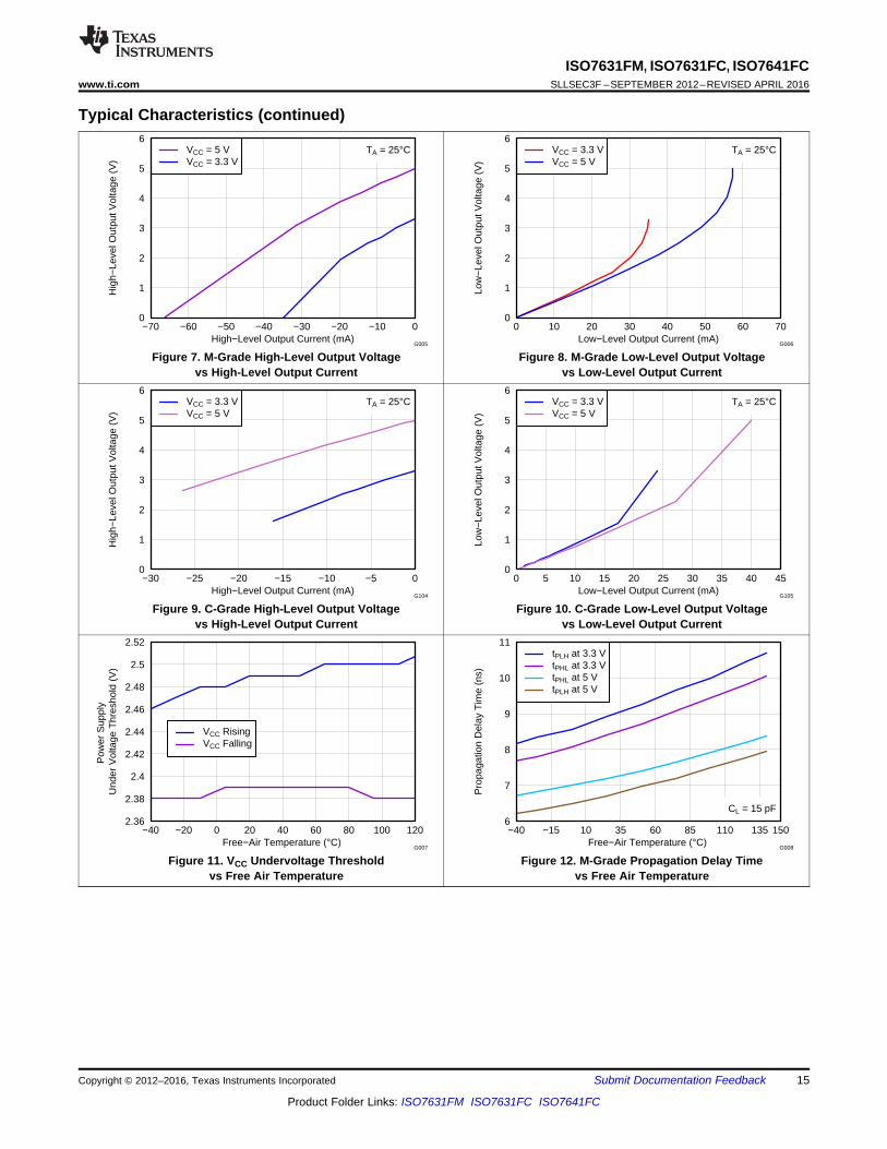
Typical Characteristics (continued)
Figure 7. M-Grade High-Level Output Voltagevs High-Level Output Current
Figure 8. M-Grade Low-Level Output Voltagevs Low-Level Output Current
Figure 9. C-Grade High-Level Output Voltagevs High-Level Output Current
Figure 10. C-Grade Low-Level Output Voltagevs Low-Level Output Current
Figure 11. VCC Undervoltage Thresholdvs Free Air Temperature
Figure 12. M-Grade Propagation Delay Timevs Free Air Temperature
0
0.2
0.4
0.6
0.8
1
1.2
1.4
0 5 10 15 20 25Data Rate (Mbps)
Pk-
Pk
Out
put J
itter
(ns
)
VCC = 3.3 VVCC = 5 V
TA = 25°CCL = 15 pFAll Channels SwitchingTyp Jitter on output pin shown
G107
0
0.1
0.2
0.3
0.4
0.5
0.6
0.7
0.8
0.9
1
0 20 40 60 80 100 120 140 160 180
Data Rate (Mbps)
Pk-P
k O
utp
ut
Jitte
r (n
s)
VCC = 5 V
VCC = 3.3 V
TA = 25°C
CL = 15 pF
All Channels Switching
Typ Jitter on output pin shown
G009
16
18
20
22
24
26
28
−40 −20 0 20 40 60 80 100 120 140Free−Air Temperature (°C)
Pro
paga
tion
Del
ay T
ime
(ns)
tPLH at 3.3 VtPHL at 3.3 VtPLH at 5 VtPHL at 5 V
CL = 15 pF
G106
16
ISO7631FM, ISO7631FC, ISO7641FCSLLSEC3F –SEPTEMBER 2012–REVISED APRIL 2016 www.ti.com
Product Folder Links: ISO7631FM ISO7631FC ISO7641FC
Submit Documentation Feedback Copyright © 2012–2016, Texas Instruments Incorporated
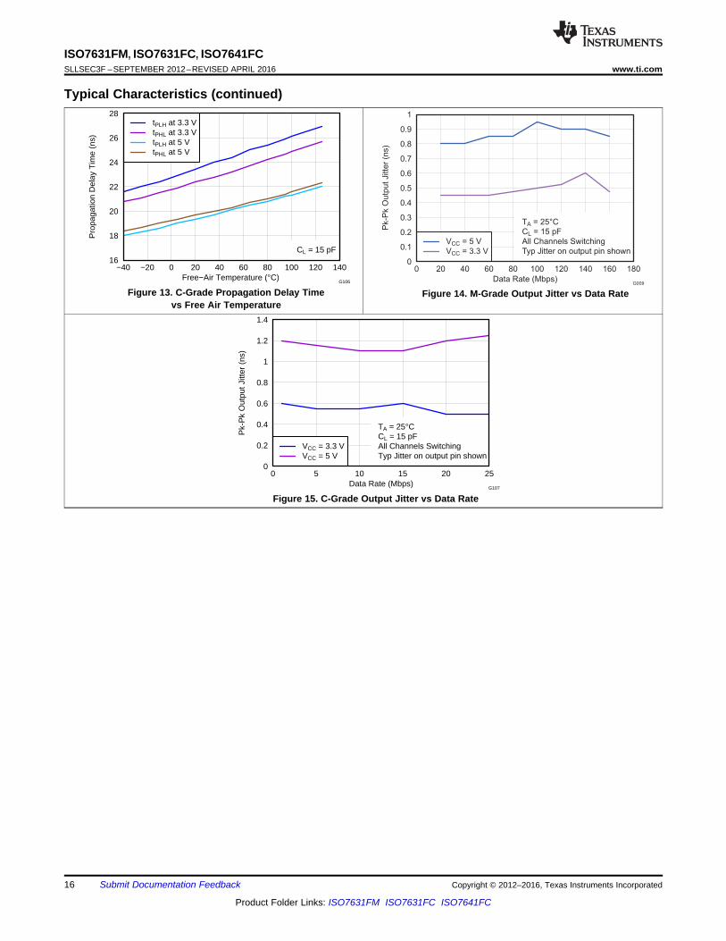
Typical Characteristics (continued)
Figure 13. C-Grade Propagation Delay Timevs Free Air Temperature
Figure 14. M-Grade Output Jitter vs Data Rate
Figure 15. C-Grade Output Jitter vs Data Rate

Input
Generator 50
OUT
RL= 1 k
EN
VO
VI
IN0V
ISO
LA
TIO
NB
AR
RIE
R
CL
W
W
1%±
NOTE A
NOTEB
0 V
VO
VI
0.5 V50%
Input
Generator 50
OUT
RL= 1 kEN
VO
VI
IN3V
ISO
LA
TIO
NB
AR
RIE
R
CL W
W
1%±
NOTE A
NOTEB
0 V
0 V
VI
50% 0.5 V
tPZH
VO
VOH
tPHZ
V /2CC V /2CC
VCC
tPZL
VCC
V /2CC
VCCO
tPLZ
VCCO
V /2CC
VOL
Copyright © 2016, Texas Instruments Incorporated
IN
ISO
LA
TIO
NB
AR
RIE
R
OUT
VO
C L
Input
Generator 50VIW
NOTE ANOTE
B 10%
90%50%
0 V
50%
VI V /2CC
VO
tPLH
VOH
tPHL
trtf
VCCI
VOL
V /2CC
Copyright © 2016, Texas Instruments Incorporated
17
ISO7631FM, ISO7631FC, ISO7641FCwww.ti.com SLLSEC3F –SEPTEMBER 2012–REVISED APRIL 2016
Product Folder Links: ISO7631FM ISO7631FC ISO7641FC
Submit Documentation FeedbackCopyright © 2012–2016, Texas Instruments Incorporated
8 Parameter Measurement Information
A. The input pulse is supplied by a generator having the following characteristics: PRR ≤ 50 kHz, 50% duty cycle, tr ≤ 3ns, tf ≤ 3ns, ZO = 50 Ω. At the input, 50 Ω resistor is required to terminate Input Generator signal. It is not needed inactual application.
B. CL = 15 pF and includes instrumentation and fixture capacitance within ±20%.
Figure 16. Switching Characteristics Test Circuit and Voltage Waveforms
A. The input pulse is supplied by a generator having the following characteristics: PRR ≤ 10 kHz, 50% duty cycle,tr ≤ 3 ns, tf ≤ 3 ns, ZO = 50 Ω.
B. CL = 15 pF and includes instrumentation and fixture capacitance within ±20%.
Figure 17. Enable/Disable Propagation Delay Time Test Circuit and Waveform

Iso
latio
n B
arr
ier
C = 0.1 F ±1%
IN
VOH or VOL
OUT
VCCI
+ –VCM
VCCOC = 0.1 F ±1%μ
GNDOGNDI
S1+
–
Pass-fail criteria –output must remainstable.
CL
μ
Note A
Copyright © 2016, Texas Instruments Incorporated
VO
OUT
ISO
LATIO
NBAR
RIE
R
NOTE A
CL
VI
IN = VCCI
0 Vt fs
fs low
VO
VI 2.7 V
50%
VCCI
VCCI
VOL
VOH
Copyright © 2016, Texas Instruments Incorporated
18
ISO7631FM, ISO7631FC, ISO7641FCSLLSEC3F –SEPTEMBER 2012–REVISED APRIL 2016 www.ti.com
Product Folder Links: ISO7631FM ISO7631FC ISO7641FC
Submit Documentation Feedback Copyright © 2012–2016, Texas Instruments Incorporated
Parameter Measurement Information (continued)
A. CL = 15 pF and includes instrumentation and fixture capacitance within ±20%.
Figure 18. Failsafe Delay Time Test Circuit and Voltage Waveforms
A. CL = 15 pF and includes instrumentation and fixture capacitance within ±20%.
Figure 19. Common-Mode Transient Immunity Test Circuit

OSC
PWM VREF
LPF
VREF
DCL
OUT
IN
0
1 S
Isolation Barrier
Low t Frequency
Channel
(DC...100 kbps)
High t Frequency
Channel
(100 kbps...150 Mbps)
Copyright © 2016, Texas Instruments Incorporated
19
ISO7631FM, ISO7631FC, ISO7641FCwww.ti.com SLLSEC3F –SEPTEMBER 2012–REVISED APRIL 2016
Product Folder Links: ISO7631FM ISO7631FC ISO7641FC
Submit Documentation FeedbackCopyright © 2012–2016, Texas Instruments Incorporated
9 Detailed Description
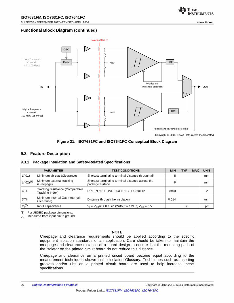
9.1 OverviewThe isolator in Figure 20 is based on a capacitive, isolation-barrier technique. The I/O channel of the deviceconsists of two internal data channels, a high-frequency channel (HF) with a bandwidth from 100 kbps up to150 Mbps, and a low-frequency channel (LF) covering the range from 100 kbps down to DC. In principle, asingle-ended input signal entering the HF-channel is split into a differential signal via the inverter gate at theinput. The following capacitor-resistor networks differentiate the signal into transients, which then are convertedinto differential pulses by two comparators. The comparator outputs drive a NOR-gate flip-flop whose outputfeeds an output multiplexer. A decision logic (DCL) at the driving output of the flip-flop measures the durationsbetween signal transients. If the duration between two consecutive transients exceeds a certain time limit, (as inthe case of a low-frequency signal), the DCL forces the output-multiplexer to switch from the high- to the low-frequency channel.
Because low-frequency input signals require the internal capacitors to assume prohibitively large values, thesesignals are pulse-width modulated (PWM) with the carrier frequency of an internal oscillator, thus creating asufficiently high frequency signal, capable of passing the capacitive barrier. As the input is modulated, a low-passfilter (LPF) is needed to remove the high-frequency carrier from the actual data before passing it on to the outputmultiplexer.
9.2 Functional Block Diagram
Figure 20. ISO7631FM Conceptual Block Diagram
OSC
PWM VREF LPF
VREF DCL
OUTIN
0
1 S
Isolation Barrier
Low t Frequency
Channel
(DC...100 kbps)
High t Frequency
Channel
(100 kbps...25 Mbps)
Polarity and
Threshold Selection
Polarity and Threshold Selection
Copyright © 2016, Texas Instruments Incorporated
20
ISO7631FM, ISO7631FC, ISO7641FCSLLSEC3F –SEPTEMBER 2012–REVISED APRIL 2016 www.ti.com
Product Folder Links: ISO7631FM ISO7631FC ISO7641FC
Submit Documentation Feedback Copyright © 2012–2016, Texas Instruments Incorporated
Functional Block Diagram (continued)
(1) Per JEDEC package dimensions.(2) Measured from input pin to ground.
Figure 21. ISO7631FC and ISO7641FC Conceptual Block Diagram
9.3 Feature Description
9.3.1 Package Insulation and Safety-Related Specifications
PARAMETER TEST CONDITIONS MIN TYP MAX UNITL(I01) Minimum air gap (Clearance) Shortest terminal to terminal distance through air 8 mm
L(I02) (1) Minimum external tracking(Creepage)
Shortest terminal to terminal distance across thepackage surface 8 mm
CTI Tracking resistance (ComparativeTracking Index) DIN EN 60112 (VDE 0303-11); IEC 60112 ≥400 V
DTI Minimum Internal Gap (InternalClearance) Distance through the insulation 0.014 mm
CI(2) Input capacitance VI = VCC/2 + 0.4 sin (2πft), f = 1MHz, VCC = 5 V 2 pF
spacer
NOTECreepage and clearance requirements should be applied according to the specificequipment isolation standards of an application. Care should be taken to maintain thecreepage and clearance distance of a board design to ensure that the mounting pads ofthe isolator on the printed circuit board do not reduce this distance.
Creepage and clearance on a printed circuit board become equal according to themeasurement techniques shown in the Isolation Glossary. Techniques such as insertinggrooves and/or ribs on a printed circuit board are used to help increase thesespecifications.

21
ISO7631FM, ISO7631FC, ISO7641FCwww.ti.com SLLSEC3F –SEPTEMBER 2012–REVISED APRIL 2016
Product Folder Links: ISO7631FM ISO7631FC ISO7641FC
Submit Documentation FeedbackCopyright © 2012–2016, Texas Instruments Incorporated
(1) Climatic Classification 40/125/21(2) All pins on each side of the barrier tied together creating a two-terminal device.
Table 1. DIN V VDE V 0884-10 (VDE V 0884-10):2006-12 Insulation Characteristics (1)
PARAMETER TEST CONDITIONS SPECIFICATION UNITVIORM Maximum working insulation voltage 1414 VPEAK
VPR Input-to-output test voltage
After Input/Output safety test subgroup 2/3,VPR = VIORM x 1.2, t = 10 s,Partial discharge < 5 pC
1697
VPEAK
Method a, After environmental tests subgroup 1,VPR = VIORM x 1.6, t = 10 s,Partial Discharge < 5 pC
2262
Method b1, 100% Production testVPR = VIORM x 1.875, t = 1 sPartial discharge < 5 pC
2652
VIOTM Maximum transient overvoltageVTEST = VIOTMt = 60 sec (Qualification)t = 1 sec (100% Production)
4242 VPEAK
RIO(2) Isolation resistance, Input to Output
VIO = 500 V, TA = 25°C >1012
ΩVIO = 500 V, 100°C ≤ TA ≤ 125°C >1011
VIO = 500 V at TS = 150°C >109
CIO(2) Barrier capacitance, Input to Output VI = 0.4 sin (2πft), f = 1MHz 2 pF
Pollution degree 2
Table 2. IEC 60664-1 Ratings TablePARAMETER TEST CONDITIONS SPECIFICATION
Material Group II
Installation classification / Overvoltagecategory for basic insulation
Rated mains voltage ≤ 300 VRMS I–IVRated mains voltage ≤ 600 VRMS I–IIIRated mains voltage ≤ 1000 VRMS I–II
(1) Production tested ≥ 3000 VRMS for 1 second in accordance with UL 1577.
Table 3. Regulatory InformationVDE TUV CSA UL CQC
Certified according toDIN V VDE V 0884-10(VDE V 0884-10):2006-12 and DIN EN 61010-1 (VDE 0411-1):2011-07
Certified according toEN/UL/CSA 60950-1 and 61010-1
Approved under CSAComponent Acceptance Notice5A, IEC 60950-1 and IEC61010-1
Recognized under 1577Component RecognitionProgram
Certified according toGB4943.1-2011
Basic InsulationMaximum TransientOvervoltage, 4242 VPKMaximum WorkingVoltage, 1414 VPK
3000 VRMS Reinforced Insulation,400 VRMS maximum workingvoltage3000 VRMS Basic Insulation, 600VRMS maximum working voltage
3000 VRMS Isolation Rating Single Protection, 2500VRMS
(1)
Reinforced Insulation, Altitude ≤5000 m, Tropical Climate, 250VRMS Maximum WorkingVoltage
Certificate number:40016131
Certificate number:U8V 13 09 77311 010
Master contract number:220991
File number: E181974 Certificate number:CQC14001109542

Ambient Temperature - (qC)
Saf
ety
Lim
iting
Cur
rent
- m
A
0 50 100 150 2000
100
200
300
400
500
600
700
D001D001
VCC1 = VCC2 = 2.7 VVCC1 = VCC2 = 3.6 VVCC1 = VCC2 = 5.5 V
22
ISO7631FM, ISO7631FC, ISO7641FCSLLSEC3F –SEPTEMBER 2012–REVISED APRIL 2016 www.ti.com
Product Folder Links: ISO7631FM ISO7631FC ISO7641FC
Submit Documentation Feedback Copyright © 2012–2016, Texas Instruments Incorporated
9.3.1.1 Safety Limiting ValuesSafety limiting intends to prevent potential damage to the isolation barrier upon failure of input or output circuitry.A failure of the IO can allow low resistance to ground or the supply and, without current limiting, dissipatesufficient power to overheat the die and damage the isolation barrier potentially leading to secondary systemfailures.
PARAMETER TEST CONDITIONS MIN TYP MAX UNIT
ISSafety input, output, or supplycurrent DW-16
θJA = 77.5 °C/W, VI = 5.5V, TJ = 150°C, TA = 25°C 293mAθJA = 77.5 °C/W, VI = 3.6V, TJ = 150°C, TA = 25°C 448
θJA = 77.5 °C/W, VI = 2.7V, TJ = 150°C, TA = 25°C 597TS Maximum safety temperature 150 °C
The safety-limiting constraint is the absolute maximum junction temperature specified in the absolute maximumratings table. The power dissipation and junction-to-air thermal impedance of the device installed in theapplication hardware determines the junction temperature. The assumed junction-to-air thermal resistance in theThermal Information table is that of a device installed on a High-K Test Board for Leaded Surface MountPackages. The power is the recommended maximum input voltage times the current. The junction temperature isthen the ambient temperature plus the power times the junction-to-air thermal resistance.
Figure 22. Thermal Derating Curve for Safety Limiting Current per VDE

OUT
8 W
13 W
IN
7.5 µA
500 W
Input Output
VCCI VCCI
VCCO
EN
1 MW
500 W
Enable
VCCO VCCO VCCO
OUT
8 W
13 W
IN
7.5 µA
500 W
Input Output
VCCI VCCI
VCCO
EN
1 MW
500 W
Enable
VCCO VCCO VCCO
Copyright © 2016, Texas Instruments Incorporated
23
ISO7631FM, ISO7631FC, ISO7641FCwww.ti.com SLLSEC3F –SEPTEMBER 2012–REVISED APRIL 2016
Product Folder Links: ISO7631FM ISO7631FC ISO7641FC
Submit Documentation FeedbackCopyright © 2012–2016, Texas Instruments Incorporated
9.4 Device Functional Modes
(1) PU = Powered Up(VCC ≥ 2.7 V); PD = Powered Down (VCC ≤ 2.1 V); X = Irrelevant; H = High Level; L= Low Level; Z = High Impedance
Table 4. Function Table (1)
INPUTVCC
OUTPUTVCC
INPUT(INx)
OUTPUT ENABLE(ENx)
OUTPUT(OUTx)
PU PU
H H or Open HL H or Open LX L Z
Open H or Open LPD PU X H or Open LPD PU X L ZPU PD X X Undetermined
Figure 23. Device I/O Schematics

14
13INA
OUTD
3
4
5
6
0.1 FEN1EN2
710
INB12
11OUTC
IND
INC
DVDD
DGND
2
GAIN124
25
26
GAIN0
SPEED
PWDN
AIN3+
AIN3-
AIN4+
A0
A1
AIN1+
AIN1-
AIN2+
SCLK
DOUT
REF+
REF-
AIN4-
1VCC1
16VCC2
2,89,15GND1GND2
23
20
19
28
8
7
27
0.1 F
P3.1
P3.0
CLK
SOMI13
11
12
14
4
2
MSP430
F2132
DVss
DVcc
0.1 F
14
13
OUTD
3
4
5
6
0.1 FNCEN
710
12
11OUTC
IND
INC
1VCC1
16VCC2
2,89,15GND1GND2
0.1 F
ISO7640
ISO7641
5VISO
5VISO
3.3V
3.3V
P3.7
P3.6
18
17
3.3V
22
AVDD
AGND
21
5VISO
0.1 F
AIN2-
13
14
17
16
15
11
12
18
INA
INBOUTB
OUTA
OUTA
OUTB
1
0.1 F0.1 F
5VISO 5VISO
Thermo
couple
Current
shunt
RTD
Bridge
XOUT
XIN
5
6
P3.415
P3.516
ADS1234
ISO-BARRIER
Copyright © 2016, Texas Instruments Incorporated
24
ISO7631FM, ISO7631FC, ISO7641FCSLLSEC3F –SEPTEMBER 2012–REVISED APRIL 2016 www.ti.com
Product Folder Links: ISO7631FM ISO7631FC ISO7641FC
Submit Documentation Feedback Copyright © 2012–2016, Texas Instruments Incorporated
10 Application and Implementation
NOTEInformation in the following applications sections is not part of the TI componentspecification, and TI does not warrant its accuracy or completeness. TI’s customers areresponsible for determining suitability of components for their purposes. Customers shouldvalidate and test their design implementation to confirm system functionality.
10.1 Application InformationISO7641FC uses single-ended TTL-logic switching technology. It has a supply voltage range from 3 V to 5.5V for both supplies, VCC1 and VCC2. When designing with digital isolators, it is important to note that due tothe single-ended design structure, digital isolators do not conform to any specific interface standard and areonly intended for isolating single-ended CMOS or TTL digital signal lines. The isolator is typically placedbetween the data controller (that is, μC or UART), and a data converter or a line transceiver, regardless ofthe interface type or standard.
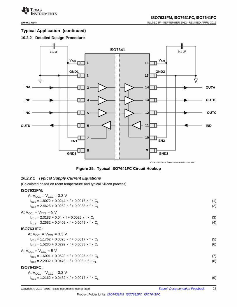
10.2 Typical Application
Figure 24. Isolated Data Acquisition System for Process Control
10.2.1 Design RequirementsUnlike optocouplers, which require external components to improve performance, provide bias, or limit current,the ISO76xx device only requires two external bypass capacitors to operate.
ISO7641
1
2
3
4
5
6
7
8
16
15
14
13
12
11
10
9
INA
INB
INC
OUTD
OUTA
OUTB
OUTC
IND
GND2
VCC2
0.1 µF
EN2
GND2
EN1
GND1
GND1
0.1 µF
VCC1
Copyright © 2016, Texas Instruments Incorporated
25
ISO7631FM, ISO7631FC, ISO7641FCwww.ti.com SLLSEC3F –SEPTEMBER 2012–REVISED APRIL 2016
Product Folder Links: ISO7631FM ISO7631FC ISO7641FC
Submit Documentation FeedbackCopyright © 2012–2016, Texas Instruments Incorporated
Typical Application (continued)10.2.2 Detailed Design Procedure
Figure 25. Typical ISO7641FC Circuit Hookup
10.2.2.1 Typical Supply Current Equations(Calculated based on room temperature and typical Silicon process)
ISO7631FM:At VCC1 = VCC2 = 3.3 V
ICC1 = 1.8072 + 0.0244 × f + 0.0016 × f × CL (1)ICC2 = 2.4625 + 0.0252 × f + 0.0033 × f × CL (2)
At VCC1 = VCC2 = 5 VICC1 = 2.3183 + 0.04 × f + 0.0025 × f × CL (3)ICC2 = 3.2582 + 0.0403 × f + 0.0049 × f × CL (4)
ISO7631FC:At VCC1 = VCC2 = 3.3 V
ICC1 = 1.1762 + 0.0325 × f + 0.0017 × f × CL (5)ICC2 = 1.5285 + 0.0299 × f + 0.0033 × f × CL (6)
At VCC1 = VCC2 = 5 VICC1 = 1.6001 + 0.0528 × f + 0.0025 × f × CL (7)ICC2 = 2.2032 + 0.0475 × f + 0.005 × f × CL (8)
ISO7641FC:At VCC1 = VCC2 = 3.3 V
ICC1 = 1.2162 + 0.0462 × f + 0.0017 × f × CL (9)

TA = 25oC, CL = 15 pF
VCC1 = VCC2 = 5 V
Pattern: NRZ 216-1
TA = 25oC, CL = 15 pF
VCC1 = VCC2 = 3.3 V
Pattern: NRZ 216-1
TA = 25oC, CL = 15 pF
VCC1 = VCC2 = 5 V
Pattern: NRZ 216-1
TA = 25oC, CL = 15 pF
VCC1 = VCC2 = 3.3 V
Pattern: NRZ 216-1
26
ISO7631FM, ISO7631FC, ISO7641FCSLLSEC3F –SEPTEMBER 2012–REVISED APRIL 2016 www.ti.com
Product Folder Links: ISO7631FM ISO7631FC ISO7641FC
Submit Documentation Feedback Copyright © 2012–2016, Texas Instruments Incorporated
Typical Application (continued)(Calculated based on room temperature and typical Silicon process)
ICC2 = 1.8054 + 0.0411 × f + 0.005 × f × CL (10)
At VCC1 = VCC2 = 5 VICC1 = 1.6583 + 0.0757 × f + 0.0025 × f × CL (11)ICC2 = 2.5008 + 0.0655 × f + 0.0076 × f × CL (12)
ICC1 and ICC2 are typical supply currents measured in mA; f is data rate measured in Mbps; CL is the capacitiveload on each channel measured in pF.
10.2.3 Application Curves
Figure 26. M-Grade Typical Eye Diagram at 150 Mbps,5 V Operation
Figure 27. M-Grade Typical Eye Diagram at 150 Mbps,3.3 V Operation
Figure 28. C-Grade Typical Eye Diagram at 25 Mbps, 5 VOperation
Figure 29. C-Grade Typical Eye Diagram at 25 Mbps, 3.3 VOperation

10 mils
10 mils
40 milsFR-4
0r ~ 4.5
Keep this
space free
from planes,
traces, pads,
and vias
Ground plane
Power plane
Low-speed traces
High-speed traces
27
ISO7631FM, ISO7631FC, ISO7641FCwww.ti.com SLLSEC3F –SEPTEMBER 2012–REVISED APRIL 2016
Product Folder Links: ISO7631FM ISO7631FC ISO7641FC
Submit Documentation FeedbackCopyright © 2012–2016, Texas Instruments Incorporated
11 Power Supply RecommendationsTo ensure reliable operation at all data rates and supply voltages, a 0.1-μF bypass capacitor is recommended atinput and output supply pins (VCC1 and VCC2). The capacitors should be placed as close to the supply pins aspossible. If only a single primary-side power supply is available in an application, isolated power can begenerated for the secondary-side with the help of a transformer driver such as Texas Instruments' SN6501. Forsuch applications, detailed power supply design and transformer selection recommendations are available inSN6501 data sheet (SLLSEA0).
12 Layout
12.1 Layout GuidelinesA minimum of four layers is required to accomplish a low EMI PCB design (see Figure 30). Layer stacking shouldbe in the following order (top-to-bottom): high-speed signal layer, ground plane, power plane and low-frequencysignal layer.• Routing the high-speed traces on the top layer avoids the use of vias (and the introduction of their
inductances) and allows for clean interconnects between the isolator and the transmitter and receiver circuitsof the data link.
• Placing a solid ground plane next to the high-speed signal layer establishes controlled impedance fortransmission line interconnects and provides an excellent low-inductance path for the return current flow.
• Placing the power plane next to the ground plane creates additional high-frequency bypass capacitance ofapproximately 100 pF/in2.
• Routing the slower speed control signals on the bottom layer allows for greater flexibility as these signal linksusually have margin to tolerate discontinuities such as vias.
If an additional supply voltage plane or signal layer is needed, add a second power and ground plane system tothe stack to keep it symmetrical. This makes the stack mechanically stable and prevents it from warping. Also thepower and ground plane of each power system can be placed closer together, thus increasing the high-frequencybypass capacitance significantly.
NOTEFor detailed layout recommendations, see Digital Isolator Design Guide, SLLA284.
12.2 Layout Example
Figure 30. Recommended Layer Stack

28
ISO7631FM, ISO7631FC, ISO7641FCSLLSEC3F –SEPTEMBER 2012–REVISED APRIL 2016 www.ti.com
Product Folder Links: ISO7631FM ISO7631FC ISO7641FC
Submit Documentation Feedback Copyright © 2012–2016, Texas Instruments Incorporated
13 Device and Documentation Support
13.1 Documentation Support
13.1.1 Related DocumentationFor related documentation, see the following:• Digital Isolator Design Guide, SLLA284• Transformer Driver for Isolated Power Supplies, SLLSEA0• Isolation Glossary, SLLA353
13.2 Related LinksThe table below lists quick access links. Categories include technical documents, support and communityresources, tools and software, and quick access to sample or buy.
Table 5. Related Links
PARTS PRODUCT FOLDER SAMPLE & BUY TECHNICALDOCUMENTS
TOOLS &SOFTWARE
SUPPORT &COMMUNITY
ISO7631FM Click here Click here Click here Click here Click hereISO7631FC Click here Click here Click here Click here Click hereISO7641FC Click here Click here Click here Click here Click here
13.3 Community ResourcesThe following links connect to TI community resources. Linked contents are provided "AS IS" by the respectivecontributors. They do not constitute TI specifications and do not necessarily reflect TI's views; see TI's Terms ofUse.
TI E2E™ Online Community TI's Engineer-to-Engineer (E2E) Community. Created to foster collaborationamong engineers. At e2e.ti.com, you can ask questions, share knowledge, explore ideas and helpsolve problems with fellow engineers.
Design Support TI's Design Support Quickly find helpful E2E forums along with design support tools andcontact information for technical support.
13.4 TrademarksDeviceNet, E2E are trademarks of Texas Instruments.All other trademarks are the property of their respective owners.
13.5 Electrostatic Discharge CautionThese devices have limited built-in ESD protection. The leads should be shorted together or the device placed in conductive foamduring storage or handling to prevent electrostatic damage to the MOS gates.
13.6 GlossarySLYZ022 — TI Glossary.
This glossary lists and explains terms, acronyms, and definitions.
14 Mechanical, Packaging, and Orderable InformationThe following pages include mechanical, packaging, and orderable information. This information is the mostcurrent data available for the designated devices. This data is subject to change without notice and revision ofthis document. For browser-based versions of this data sheet, refer to the left-hand navigation.

www.ti.com
PACKAGE OUTLINE
C
TYP10.639.97
2.65 MAX
14X 1.27
16X0.510.31
2X
8.89
TYP0.380.25
0 - 80.30.1
(1.4)
0.25
GAGE PLANE
1.270.40
A
NOTE 3
10.510.1
B
NOTE 4
7.67.4
4221009/A 08/2013
SOIC - 2.65 mm max heightDW0016BSOIC
NOTES:
1. All linear dimensions are in millimeters. Dimensions in parenthesis are for reference only. Dimensioning and tolerancingper ASME Y14.5M.
2. This drawing is subject to change without notice.3. This dimension does not include mold flash, protrusions, or gate burrs. Mold flash, protrusions, or gate burrs shall not
exceed 0.15 mm, per side.4. This dimension does not include interlead flash. Interlead flash shall not exceed 0.25 mm, per side.5. Reference JEDEC registration MO-013, variation AA.
116
0.25 C A B
98
PIN 1 IDAREA
SEATING PLANE
0.1 C
SEE DETAIL A
TYPICALDETAIL A
SCALE 1.500
29
ISO7631FM, ISO7631FC, ISO7641FCwww.ti.com SLLSEC3F –SEPTEMBER 2012–REVISED APRIL 2016
Product Folder Links: ISO7631FM ISO7631FC ISO7641FC
Submit Documentation FeedbackCopyright © 2012–2016, Texas Instruments Incorporated
www.ti.com
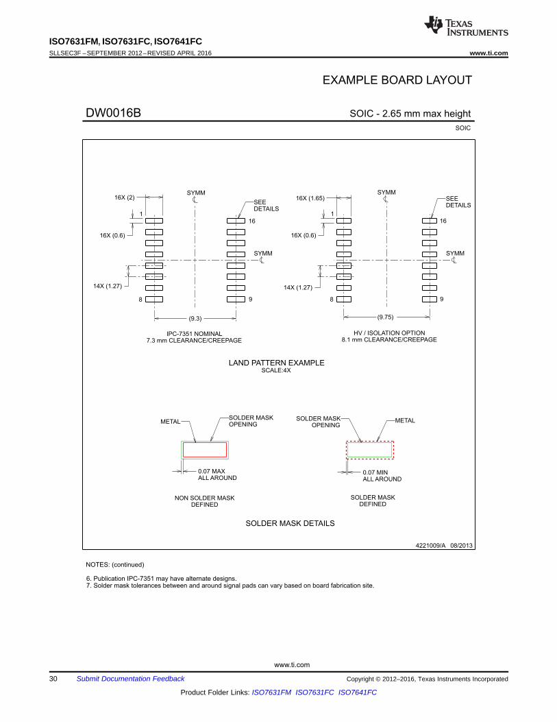
EXAMPLE BOARD LAYOUT
(9.75)
0.07 MAXALL AROUND
0.07 MINALL AROUND
(9.3)
14X (1.27)
16X (1.65)
16X (0.6)
14X (1.27)
16X (2)
16X (0.6)
4221009/A 08/2013
SYMM
SOIC - 2.65 mm max heightDW0016BSOIC
SYMM
SEEDETAILS
1
8 9
16
SYMM
HV / ISOLATION OPTION8.1 mm CLEARANCE/CREEPAGE
NOTES: (continued)
6. Publication IPC-7351 may have alternate designs.7. Solder mask tolerances between and around signal pads can vary based on board fabrication site.
METALSOLDER MASKOPENING
NON SOLDER MASKDEFINED
OPENING
SOLDER MASK DETAILS
SOLDER MASK METAL
SOLDER MASKDEFINED
SCALE:4XLAND PATTERN EXAMPLE
SYMM
1
8 9
16
IPC-7351 NOMINAL7.3 mm CLEARANCE/CREEPAGE
SEEDETAILS
30
ISO7631FM, ISO7631FC, ISO7641FCSLLSEC3F –SEPTEMBER 2012–REVISED APRIL 2016 www.ti.com
Product Folder Links: ISO7631FM ISO7631FC ISO7641FC
Submit Documentation Feedback Copyright © 2012–2016, Texas Instruments Incorporated

www.ti.com
EXAMPLE STENCIL DESIGN
16X (1.65)
16X (0.6)
14X (1.27)
(9.75)
16X (2)
16X (0.6)
14X (1.27)
(9.3)
4221009/A 08/2013
SOIC - 2.65 mm max heightDW0016BSOIC
NOTES: (continued)
8. Laser cutting apertures with trapezoidal walls and rounded corners may offer better paste release. IPC-7525 may have alternatedesign recommendations.
9. Board assembly site may have different recommendations for stencil design.
SYMM
SYMM
1
8 9
16
HV / ISOLATION OPTION8.1 mm CLEARANCE/CREEPAGE
BASED ON 0.125 mm THICK STENCILSOLDER PASTE EXAMPLE
SCALE:4X
SYMM
SYMM
1
8 9
16
IPC-7351 NOMINAL7.3 mm CLEARANCE/CREEPAGE
31
ISO7631FM, ISO7631FC, ISO7641FCwww.ti.com SLLSEC3F –SEPTEMBER 2012–REVISED APRIL 2016
Product Folder Links: ISO7631FM ISO7631FC ISO7641FC
Submit Documentation FeedbackCopyright © 2012–2016, Texas Instruments Incorporated

PACKAGE OPTION ADDENDUM
www.ti.com 28-Mar-2016
Addendum-Page 1
PACKAGING INFORMATION
Orderable Device Status(1)
Package Type PackageDrawing
Pins PackageQty
Eco Plan(2)
Lead/Ball Finish(6)
MSL Peak Temp(3)
Op Temp (°C) Device Marking(4/5)
Samples
ISO7631FCDW ACTIVE SOIC DW 16 40 Green (RoHS& no Sb/Br)
CU NIPDAU Level-3-260C-168 HR -40 to 125 ISO7631FC
ISO7631FCDWR ACTIVE SOIC DW 16 2000 Green (RoHS& no Sb/Br)
CU NIPDAU Level-3-260C-168 HR -40 to 125 ISO7631FC
ISO7631FMDW ACTIVE SOIC DW 16 40 Green (RoHS& no Sb/Br)
CU NIPDAU Level-3-260C-168 HR -40 to 125 ISO7631FM
ISO7631FMDWR ACTIVE SOIC DW 16 2000 Green (RoHS& no Sb/Br)
CU NIPDAU Level-3-260C-168 HR -40 to 125 ISO7631FM
ISO7641FCDW ACTIVE SOIC DW 16 40 Green (RoHS& no Sb/Br)
CU NIPDAU Level-3-260C-168 HR -40 to 125 ISO7641FC
ISO7641FCDWR ACTIVE SOIC DW 16 2000 Green (RoHS& no Sb/Br)
CU NIPDAU Level-3-260C-168 HR -40 to 125 ISO7641FC
(1) The marketing status values are defined as follows:ACTIVE: Product device recommended for new designs.LIFEBUY: TI has announced that the device will be discontinued, and a lifetime-buy period is in effect.NRND: Not recommended for new designs. Device is in production to support existing customers, but TI does not recommend using this part in a new design.PREVIEW: Device has been announced but is not in production. Samples may or may not be available.OBSOLETE: TI has discontinued the production of the device.
(2) Eco Plan - The planned eco-friendly classification: Pb-Free (RoHS), Pb-Free (RoHS Exempt), or Green (RoHS & no Sb/Br) - please check http://www.ti.com/productcontent for the latest availabilityinformation and additional product content details.TBD: The Pb-Free/Green conversion plan has not been defined.Pb-Free (RoHS): TI's terms "Lead-Free" or "Pb-Free" mean semiconductor products that are compatible with the current RoHS requirements for all 6 substances, including the requirement thatlead not exceed 0.1% by weight in homogeneous materials. Where designed to be soldered at high temperatures, TI Pb-Free products are suitable for use in specified lead-free processes.Pb-Free (RoHS Exempt): This component has a RoHS exemption for either 1) lead-based flip-chip solder bumps used between the die and package, or 2) lead-based die adhesive used betweenthe die and leadframe. The component is otherwise considered Pb-Free (RoHS compatible) as defined above.Green (RoHS & no Sb/Br): TI defines "Green" to mean Pb-Free (RoHS compatible), and free of Bromine (Br) and Antimony (Sb) based flame retardants (Br or Sb do not exceed 0.1% by weightin homogeneous material)
(3) MSL, Peak Temp. - The Moisture Sensitivity Level rating according to the JEDEC industry standard classifications, and peak solder temperature.
(4) There may be additional marking, which relates to the logo, the lot trace code information, or the environmental category on the device.
(5) Multiple Device Markings will be inside parentheses. Only one Device Marking contained in parentheses and separated by a "~" will appear on a device. If a line is indented then it is a continuationof the previous line and the two combined represent the entire Device Marking for that device.
PACKAGE OPTION ADDENDUM
www.ti.com 28-Mar-2016
Addendum-Page 2
(6) Lead/Ball Finish - Orderable Devices may have multiple material finish options. Finish options are separated by a vertical ruled line. Lead/Ball Finish values may wrap to two lines if the finishvalue exceeds the maximum column width.
Important Information and Disclaimer:The information provided on this page represents TI's knowledge and belief as of the date that it is provided. TI bases its knowledge and belief on informationprovided by third parties, and makes no representation or warranty as to the accuracy of such information. Efforts are underway to better integrate information from third parties. TI has taken andcontinues to take reasonable steps to provide representative and accurate information but may not have conducted destructive testing or chemical analysis on incoming materials and chemicals.TI and TI suppliers consider certain information to be proprietary, and thus CAS numbers and other limited information may not be available for release.
In no event shall TI's liability arising out of such information exceed the total purchase price of the TI part(s) at issue in this document sold by TI to Customer on an annual basis.

TAPE AND REEL INFORMATION
*All dimensions are nominal
Device PackageType
PackageDrawing
Pins SPQ ReelDiameter
(mm)
ReelWidth
W1 (mm)
A0(mm)
B0(mm)
K0(mm)
P1(mm)
W(mm)
Pin1Quadrant
ISO7631FCDWR SOIC DW 16 2000 330.0 16.4 10.75 10.7 2.7 12.0 16.0 Q1
ISO7631FMDWR SOIC DW 16 2000 330.0 16.4 10.75 10.7 2.7 12.0 16.0 Q1
ISO7641FCDWR SOIC DW 16 2000 330.0 16.4 10.75 10.7 2.7 12.0 16.0 Q1
PACKAGE MATERIALS INFORMATION
www.ti.com 28-Mar-2016
Pack Materials-Page 1
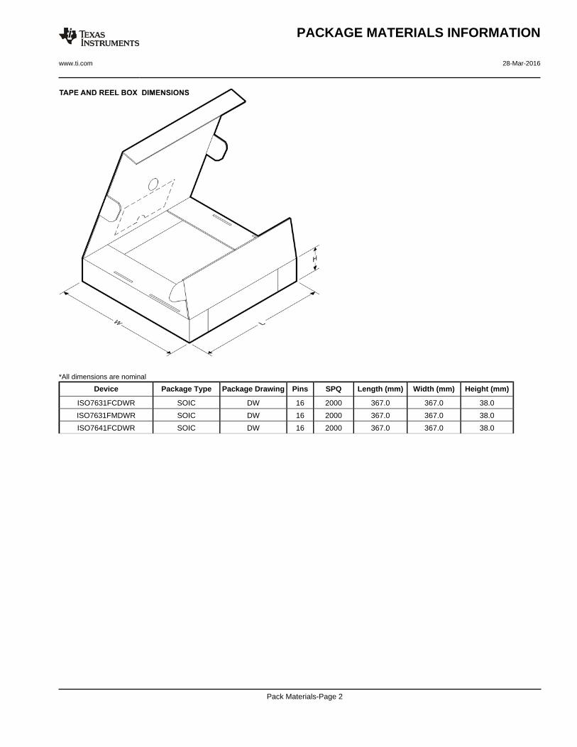
*All dimensions are nominal
Device Package Type Package Drawing Pins SPQ Length (mm) Width (mm) Height (mm)
ISO7631FCDWR SOIC DW 16 2000 367.0 367.0 38.0
ISO7631FMDWR SOIC DW 16 2000 367.0 367.0 38.0
ISO7641FCDWR SOIC DW 16 2000 367.0 367.0 38.0
PACKAGE MATERIALS INFORMATION
www.ti.com 28-Mar-2016
Pack Materials-Page 2
IMPORTANT NOTICE
Texas Instruments Incorporated and its subsidiaries (TI) reserve the right to make corrections, enhancements, improvements and otherchanges to its semiconductor products and services per JESD46, latest issue, and to discontinue any product or service per JESD48, latestissue. Buyers should obtain the latest relevant information before placing orders and should verify that such information is current andcomplete. All semiconductor products (also referred to herein as “components”) are sold subject to TI’s terms and conditions of salesupplied at the time of order acknowledgment.TI warrants performance of its components to the specifications applicable at the time of sale, in accordance with the warranty in TI’s termsand conditions of sale of semiconductor products. Testing and other quality control techniques are used to the extent TI deems necessaryto support this warranty. Except where mandated by applicable law, testing of all parameters of each component is not necessarilyperformed.TI assumes no liability for applications assistance or the design of Buyers’ products. Buyers are responsible for their products andapplications using TI components. To minimize the risks associated with Buyers’ products and applications, Buyers should provideadequate design and operating safeguards.TI does not warrant or represent that any license, either express or implied, is granted under any patent right, copyright, mask work right, orother intellectual property right relating to any combination, machine, or process in which TI components or services are used. Informationpublished by TI regarding third-party products or services does not constitute a license to use such products or services or a warranty orendorsement thereof. Use of such information may require a license from a third party under the patents or other intellectual property of thethird party, or a license from TI under the patents or other intellectual property of TI.Reproduction of significant portions of TI information in TI data books or data sheets is permissible only if reproduction is without alterationand is accompanied by all associated warranties, conditions, limitations, and notices. TI is not responsible or liable for such altereddocumentation. Information of third parties may be subject to additional restrictions.Resale of TI components or services with statements different from or beyond the parameters stated by TI for that component or servicevoids all express and any implied warranties for the associated TI component or service and is an unfair and deceptive business practice.TI is not responsible or liable for any such statements.Buyer acknowledges and agrees that it is solely responsible for compliance with all legal, regulatory and safety-related requirementsconcerning its products, and any use of TI components in its applications, notwithstanding any applications-related information or supportthat may be provided by TI. Buyer represents and agrees that it has all the necessary expertise to create and implement safeguards whichanticipate dangerous consequences of failures, monitor failures and their consequences, lessen the likelihood of failures that might causeharm and take appropriate remedial actions. Buyer will fully indemnify TI and its representatives against any damages arising out of the useof any TI components in safety-critical applications.In some cases, TI components may be promoted specifically to facilitate safety-related applications. With such components, TI’s goal is tohelp enable customers to design and create their own end-product solutions that meet applicable functional safety standards andrequirements. Nonetheless, such components are subject to these terms.No TI components are authorized for use in FDA Class III (or similar life-critical medical equipment) unless authorized officers of the partieshave executed a special agreement specifically governing such use.Only those TI components which TI has specifically designated as military grade or “enhanced plastic” are designed and intended for use inmilitary/aerospace applications or environments. Buyer acknowledges and agrees that any military or aerospace use of TI componentswhich have not been so designated is solely at the Buyer's risk, and that Buyer is solely responsible for compliance with all legal andregulatory requirements in connection with such use.TI has specifically designated certain components as meeting ISO/TS16949 requirements, mainly for automotive use. In any case of use ofnon-designated products, TI will not be responsible for any failure to meet ISO/TS16949.
Products ApplicationsAudio www.ti.com/audio Automotive and Transportation www.ti.com/automotiveAmplifiers amplifier.ti.com Communications and Telecom www.ti.com/communicationsData Converters dataconverter.ti.com Computers and Peripherals www.ti.com/computersDLP® Products www.dlp.com Consumer Electronics www.ti.com/consumer-appsDSP dsp.ti.com Energy and Lighting www.ti.com/energyClocks and Timers www.ti.com/clocks Industrial www.ti.com/industrialInterface interface.ti.com Medical www.ti.com/medicalLogic logic.ti.com Security www.ti.com/securityPower Mgmt power.ti.com Space, Avionics and Defense www.ti.com/space-avionics-defenseMicrocontrollers microcontroller.ti.com Video and Imaging www.ti.com/videoRFID www.ti-rfid.comOMAP Applications Processors www.ti.com/omap TI E2E Community e2e.ti.comWireless Connectivity www.ti.com/wirelessconnectivity
Mailing Address: Texas Instruments, Post Office Box 655303, Dallas, Texas 75265Copyright © 2016, Texas Instruments Incorporated